US4890146A - High voltage level shift semiconductor device - Google Patents
High voltage level shift semiconductor deviceDownload PDFInfo
- Publication number
- US4890146A US4890146AUS07/133,710US13371087AUS4890146AUS 4890146 AUS4890146 AUS 4890146AUS 13371087 AUS13371087 AUS 13371087AUS 4890146 AUS4890146 AUS 4890146A
- Authority
- US
- United States
- Prior art keywords
- region
- conductivity type
- drain resistor
- extending
- epitaxial layer
- Prior art date
- Legal status (The legal status is an assumption and is not a legal conclusion. Google has not performed a legal analysis and makes no representation as to the accuracy of the status listed.)
- Expired - Lifetime
Links
- 239000004065semiconductorSubstances0.000titleclaimsabstractdescription42
- 210000000746body regionAnatomy0.000claimsdescription209
- 239000000758substrateSubstances0.000claimsdescription130
- 238000002955isolationMethods0.000claimsdescription107
- 239000011810insulating materialSubstances0.000claimsdescription91
- 239000000463materialSubstances0.000claimsdescription39
- 238000001465metallisationMethods0.000description23
- OAICVXFJPJFONN-UHFFFAOYSA-NPhosphorusChemical compound[P]OAICVXFJPJFONN-UHFFFAOYSA-N0.000description14
- 238000009792diffusion processMethods0.000description14
- 229910052698phosphorusInorganic materials0.000description14
- 239000011574phosphorusSubstances0.000description14
- 238000000034methodMethods0.000description11
- 229910021420polycrystalline siliconInorganic materials0.000description7
- 229920005591polysiliconPolymers0.000description7
- 229910052787antimonyInorganic materials0.000description5
- WATWJIUSRGPENY-UHFFFAOYSA-Nantimony atomChemical compound[Sb]WATWJIUSRGPENY-UHFFFAOYSA-N0.000description5
- 239000002019doping agentSubstances0.000description5
- VYPSYNLAJGMNEJ-UHFFFAOYSA-NSilicium dioxideChemical compoundO=[Si]=OVYPSYNLAJGMNEJ-UHFFFAOYSA-N0.000description4
- 230000015556catabolic processEffects0.000description4
- 230000000873masking effectEffects0.000description3
- 229910052751metalInorganic materials0.000description3
- 239000002184metalSubstances0.000description3
- 230000015572biosynthetic processEffects0.000description2
- 238000010276constructionMethods0.000description2
- 238000007796conventional methodMethods0.000description2
- 238000002513implantationMethods0.000description2
- 235000012239silicon dioxideNutrition0.000description2
- 239000000377silicon dioxideSubstances0.000description2
- 238000012876topographyMethods0.000description2
- ZOXJGFHDIHLPTG-UHFFFAOYSA-NBoronChemical compound[B]ZOXJGFHDIHLPTG-UHFFFAOYSA-N0.000description1
- 229910001439antimony ionInorganic materials0.000description1
- 229910052785arsenicInorganic materials0.000description1
- RQNWIZPPADIBDY-UHFFFAOYSA-Narsenic atomChemical compound[As]RQNWIZPPADIBDY-UHFFFAOYSA-N0.000description1
- 229910052796boronInorganic materials0.000description1
- 239000012141concentrateSubstances0.000description1
- 230000000694effectsEffects0.000description1
- 230000005684electric fieldEffects0.000description1
- 230000008030eliminationEffects0.000description1
- 238000003379elimination reactionMethods0.000description1
- 230000001747exhibiting effectEffects0.000description1
- 238000004519manufacturing processMethods0.000description1
- 238000000059patterningMethods0.000description1
- 238000012358sourcingMethods0.000description1
Images


Classifications
- H—ELECTRICITY
- H10—SEMICONDUCTOR DEVICES; ELECTRIC SOLID-STATE DEVICES NOT OTHERWISE PROVIDED FOR
- H10D—INORGANIC ELECTRIC SEMICONDUCTOR DEVICES
- H10D84/00—Integrated devices formed in or on semiconductor substrates that comprise only semiconducting layers, e.g. on Si wafers or on GaAs-on-Si wafers
- H10D84/80—Integrated devices formed in or on semiconductor substrates that comprise only semiconducting layers, e.g. on Si wafers or on GaAs-on-Si wafers characterised by the integration of at least one component covered by groups H10D12/00 or H10D30/00, e.g. integration of IGFETs
- H10D84/811—Combinations of field-effect devices and one or more diodes, capacitors or resistors
- H—ELECTRICITY
- H10—SEMICONDUCTOR DEVICES; ELECTRIC SOLID-STATE DEVICES NOT OTHERWISE PROVIDED FOR
- H10D—INORGANIC ELECTRIC SEMICONDUCTOR DEVICES
- H10D30/00—Field-effect transistors [FET]
- H10D30/60—Insulated-gate field-effect transistors [IGFET]
- H10D30/601—Insulated-gate field-effect transistors [IGFET] having lightly-doped drain or source extensions, e.g. LDD IGFETs or DDD IGFETs
- H10D30/603—Insulated-gate field-effect transistors [IGFET] having lightly-doped drain or source extensions, e.g. LDD IGFETs or DDD IGFETs having asymmetry in the channel direction, e.g. lateral high-voltage MISFETs having drain offset region or extended drain IGFETs [EDMOS]
- H—ELECTRICITY
- H10—SEMICONDUCTOR DEVICES; ELECTRIC SOLID-STATE DEVICES NOT OTHERWISE PROVIDED FOR
- H10D—INORGANIC ELECTRIC SEMICONDUCTOR DEVICES
- H10D64/00—Electrodes of devices having potential barriers
- H10D64/20—Electrodes characterised by their shapes, relative sizes or dispositions
- H10D64/27—Electrodes not carrying the current to be rectified, amplified, oscillated or switched, e.g. gates
- H10D64/311—Gate electrodes for field-effect devices
- H10D64/411—Gate electrodes for field-effect devices for FETs
- H10D64/511—Gate electrodes for field-effect devices for FETs for IGFETs
- H10D64/517—Gate electrodes for field-effect devices for FETs for IGFETs characterised by the conducting layers
- H10D64/519—Gate electrodes for field-effect devices for FETs for IGFETs characterised by the conducting layers characterised by their top-view geometrical layouts
Definitions
- This inventionrelates to high voltage integrated circuit semiconductor devices and more particularly to level shift high voltage semiconductor devices.
- HVIChigh voltage integrated circuits
- the gate of the devicemust be driven on and off relative to this high voltage supply.
- a P-channel devicecan be turned on by pulling its gate 20 volts below its source. If a 200 volt supply is used, the gate would be pulled down to 180v Similarly, it can be turned off by taking the gate potential to the 200 volt supply potential.
- the control signals normally available for turning devices on and offare referenced to ground and vary between 0 to 20 volts (or in some cases between 0 and 5 volts).
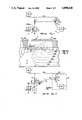
- resistor-load inverter circuit 1includes low voltage logic input circuit 2, depicted in FIG.
- Transistor 3includes gate 4, which receives control signals from logic input circuit 2, source 5 which is connected to body 6, both of which are commonly connected to ground and drain 7 which is connected to the lower side of resistor 8.
- the upper side of resistor 8is connected to a positive high voltage line, which would typically be between 100 volts and 500 volts, obtained from supply from pad 9.
- high voltage P-channel transistor 10is included having its gate 11 connected to a tap (unnumbered) of resistor 8, its source 12 and body 13, which are commonly connected, which are tied to the positive high voltage supply.
- Transistor 10also includes drain 14 which is connected to output pad 15. As mentioned above, it is desired to turn device 10 "on” and “off” which requires bringing gate 11 to approximately 20 volts below the potential on the +HV line to turn device 10 "on”, and returning gate 11 to the +HV volt supply potential to turn device 10 "off”.
- Shifting gate 11 of device 10 between the above-mentioned voltagesis accomplished by appropriate control signals to gate 4 of device 3 to turn device 3 "on” and “off” changing the potential at the tap of resistor 8, causing the potential on gate 11 to shift between the +HV supply potential when device 3 is “off” and to drop to approximately 20 volts below the +HV supply potential when device 3 is “on".
- the P-channel device in circuit 1is shown as an MOS transistor, such a circuit may also be implemented using a PNP bipolar transistor instead of transistor 10, however the circuitry may be different.
- metal interconnectsTo implement high voltage level shift circuit 1 monolithically, metal interconnects must cross high-voltage PN junctions. When a metal interconnect crosses a high voltage PN junction, it concentrates electric fields which can lead to breakdown at the junction. Techniques are available to field plate the high voltage junction to alleviate the problems caused by a high voltage interconnect crossing above the junction, but the field plate technique is increasingly difficult to implement at higher voltages and may be incompatible with certain wafer fabrication processes.
- FIG. 2illustrates the cross-section of a portion of a lightly doped drain of N-channel device 3 having source 5 and body 6 shorted by metallization 22 as described above with respect to circuit 1.
- the reverse biased equipotentialsare illustrated for the "off" state condition. More particularly, it will be noted that since drain 7 is connected via metallization 18 to high voltage (through resistor 8, not shown), equipotential lines varying from 0 volts to 180 volts are distributed across substrate 19 and pose a crowding problem in region 20 where the equipotential lines converge near the lightly doped end of drain extension 7a. With the converging of these lines at junction 21 (the PN junction between substrate 19 and drain extension 7a) the likelihood of breakdown in this region is dramatically increased.
- circuit 1utilizing a self-isolated high voltage integrated circuit process will result in at least four high-voltage interconnect points which will occur on the topography required to monolithically implement circuit 1.
- the term "self-isolated”is used because, with respect to FIG. 2 for example, drain 7 forms back-to-back diodes with the drain of any adjacent N-channel device.
- FIGS. 3 and 4(which will be described after FIG. 3) show a typical implementation of circuit 1. Referring to FIG.
- these interconnect pointsare illustrated on the schematic by including dashed lines representing N-well regions 28 and 30, and more specifically include point 25, which is the high voltage crossing of metallization 18 to drain 7 of N-channel transistor 3; point 26 where metallization 18 crosses the P substrate (which is below metallization 18) leading to the junction with resistor 8; point 27 where metallization 44 crosses into N-well 28 to the tap point (unnumbered) of resistor 8; and point 29 where metallization 44 crosses the PN junction to reach N-well region 30 where metallization 44 connects to gate 11 of P-channel transistor 10.
- the P-channel devicemay be self-isolated in an N-well region or be a DMOS device with N+isolation region, in which case there will be a high voltage crossing of the N+isolation region.
- the high voltage supply bonding pad 9is not located inside N-well region 28, high voltage crossing point 31 will be encountered, and similarly, if the high voltage crossing to source 12/body 13 connection on P-channel device 10 is outside of region 30, high voltage crossing point 32 will also occur.
- Common ground bus 34runs along the lower edge of cell 35 and is connected to body 6 and source 5 of N-channel device 3 at connection points 36 and 37, respectively, and is also connected to logic block 2. Via metallization 38, logic block 2 is connected to gate 4 of N-channel device 3. Bus 39 connects drain 7 to a connection point 40 of resistor 8 in circuit 1. It will be appreciated that with these connections, crossing points 25 and 26 (indicated in FIG. 4 by dashed lines to denote the regionlike nature of the crossing points) are encountered.
- resistor 8is fabricated through the use of N-well regions 28a and 28b, which are located within guard ring 41 of highly P-doped material. Regions 28a and 28b may be formed, for example, by a diffusion process and would be N-doped regions in P-type substrate 19. Contact points 42 and 43 connect metallization 44 to regions 28a and 28b and form the tap connection to resistor 8. Bus 44 continues above substrate 19 and crosses above the junction between substrate 19 and N region 30, and connects to gate 11 of P channel device 10. This routing of metallization 44 results in crossing point 27 and crossing point 29. Positive high voltage bus 45 provides connection to region 28b of resistor 8 and results in crossing point 31 and 31'. Crossing point 32 from high voltage pad 9 into N-well region 30 may also be noted by reference to FIG. 4.
- a semiconductor devicecomprising a substrate of first conductivity type, a body region of first conductivity type extending into said substrate from a surface, said body region having a doping level greater than the doping level of said substrate, a source region of second conductivity type extending into said body region from said surface to a depth less than said body region extends into said substrate, a combined drain resistor region of second conductivity type extending into said substrate from said surface and being positioned adjacent to said body region, said combined drain resistor region functioning as a drain region for said device and as a resistive region, a channel region in said substrate extending to said surface between said combined drain resistor region and said body region, a channel region in said body region extending to said surface between said source region and said channel region in said substrate, an insulating material on said surface and extending from said source region to said combined drain resistor region, a gate on said insulating material, said gate being positioned above said channel region in said body region and said channel region in said substrate.
- the combined drain resistor regionincludes a first portion, adjacent to the channel region in the substrate, which extends into the substrate to a first depth and a second portion away from said channel region which extends into the substrate to a second depth greater than the first depth.
- a device in accordance with the two above-mentioned featureswhich also includes a source region of first conductivity type extending into said second portion of said combined drain resistor region from said surface, a drain region of first conductivity type extending into said second portion of said combined drain resistor region from said surface and being positioned adjacent to said source region of first conductivity type, a channel region in said second portion of said combined drain resistor region extending to said surface between said source region of first conductivity type and said drain region of first conductivity type, an insulating material on said surface above said channel region in said second portion of said combined drain resistor region, and a gate on said insulating material above said channel region in said second portion of said combined drain resistor region.
- a device in accordance with the foregoing featuresand also provide such device with a first contact region of second conductivity type extending into said second portion of said combined drain resistor region from said surface and means electrically connecting said first contact region to said gate positioned above said channel region in said second portion of said combined drain resistor region.
- a semiconductor devicecomprising a substrate of first conductivity type, an epitaxial layer of material of first conductivity type on said substrate, a body region of first conductivity type extending into said epitaxial layer from a surface, said body region having a doping level greater than the doping level of said epitaxial layer, a source region of second conductivity type extending into said body region from said surface to a depth less than said body region extends into said epitaxial layer, a combined drain resistor region of second conductivity type extending into said epitaxial layer from said surface and being positioned adjacent to said body region, said combined drain resistor region functioning as a drain region for said device and as a resistive region, a channel region in said epitaxial layer extending to said surface between said combined drain resistor region and said body region, a channel region in said body region extending to said surface between said source region and said channel region in said epitaxial layer, an insulating material on said surface extending from said source region to said combined drain resistor region,
- a deviceas set forth in the immediately preceding paragraph which includes a first contact region of second conductivity type extending into said combined drain resistor region from said surface and means electrically connecting said first contact region to said second gate.
- a device as described in the first feature abovewhich also includes in the combined drain resistor region a source region of first conductivity type extending into said combined drain resistor region from said surface, a drain region of first conductivity type extending into said combined drain resistor region from said surface and being positioned adjacent to said source region of first conductivity type, a channel region in said combined drain resistor region extending to said surface between said source region of first conductivity type in said drain region of first conductivity type, an insulating material on said surface above said channel region in said combined drain resistor region and a gate on said insulating material above said channel region in said combined drain resistor region.
- a device of the type immediately set forth abovewhich includes a first contact region of second conductivity type in said combined drain resistor region and means electrically connecting said first contact region to said gate positioned above said channel region in said combined drain resistor region.
- a semiconductor devicecomprising a substrate of first conductivity type, an epitaxial layer of material of first conductivity type on said substrate, a body region of first conductivity type extending into said epitaxial layer from a surface, said body region having a doping level greater than the doping level of said epitaxial layer, a source region of second conductivity type extending into said body region from said surface to a depth less than said body region extends into said epitaxial layer, a combined drain resistor region of second conductivity type extending into said epitaxial layer from said surface and being positioned adjacent to said body region, said combined drain resistor region functioning as a drain region for said device and as a resistive region, a channel region in said epitaxial layer extending to said surface between said combined drain resistor region and said body region, a channel region in said body region extending to said surface between said source region and said channel region in said epitaxial layer, an insulating material on said surface extending from said source region to said combined drain resistor region
- a semiconductor device of the type set forth abovehaving a bipolar transistor and include a first contact region of second conductivity type extending into said combined drain resistor region from said surface and means electrically connecting said first contact region to said base region of said bipolar transistor.
- a semiconductor devicecomprising a substrate of first conductivity type; an epitaxial layer of material of first conductivity type on said substrate; a body region of first conductivity type extending into said epitaxial layer from a surface, said body region having a doping level greater than the doping level of said epitaxial layer; a source region of second conductivity type extending into said body region from said surface to a depth less than said body region extends into said epitaxial layer; a combined drain resistor region of second conductivity type extending into said epitaxial layer from said surface and being positioned adjacent to said body region, said combined drain resistor region functioning as a drain region for said device and as a resistive region; a channel region in said body region extending to said surface between said source region and said combined drain resistor region; an insulating material on said surface above said channel region in said body region; a first gate on said insulating material, said first gate being positioned above said channel region in said body region; a first isolation region of second conductivity type
- a semiconductor devicecomprising a substrate of first conductivity type, an epitaxial layer of material of second conductivity type on said substrate, a body region of second conductivity type extending into said epitaxial layer from a surface, said body region having a doping level greater than the doping level of said epitaxial layer, a source region of first conductivity type extending into said body region from said surface to a depth less than said body region extends into said substrate, a combined drain resistor region of first conductivity type extending into said epitaxial layer from said surface and being positioned adjacent to said body region, said combined drain resistor region functioning as a drain region for said device and as a resistive region, a channel region in said epitaxial layer extending to said surface between said combined drain resistor region and said body region, a channel region in said body region extending to said surface between said source region and said channel region in said epitaxial layer, an insulating material on said surface and extending from said source region to said combined drain resistor region, a first gate
- a deviceas set forth immediately above which includes a contact region of second conductivity type in said combined drain resistor region and means electrically connecting said contact region to said second gate.
- a semiconductor devicecomprising a substrate of first conductivity type, an epitaxial layer of material of first conductivity type on said substrate, a body region of first conductivity type extending into said epitaxial layer from a surface, said body region having a doping level greater than the doping level of said epitaxial layer, a source region of second conductivity type extending into said body region from said surface to a depth less than said body region extends into said epitaxial layer, a combined drain resistor region of second conductivity type extending into said epitaxial layer from said surface and being positioned adjacent to said body region, said combined drain resistor region functioning as a drain region for said device and as a resistive region, a channel region in said body region extending to said surface between said source region and said combined drain resistor region, an insulating material on said surface above said channel region in said body region, a first gate on said insulating material, said first gate being positioned above said channel region in said body region, a first isolation region of second
- a semiconductor devicecomprising a substrate of first conductivity type, a first epitaxial layer of material of first conductivity type on said substrate, a second epitaxial layer of material of first conductivity type on said first epitaxial layer, a body region of first conductivity type extending into said second epitaxial layer from a surface, said body region having a doping level greater than the doping level of said second epitaxial layer, a source region of second conductivity type extending into said body region from said surface to a depth less than said body region extends into said second epitaxial layer, a combined drain resistor region of second conductivity type extending into said second epitaxial layer from said surface and being positioned adjacent to said body region, said combined drain resistor region functioning as a drain region for said device and as a resistive region, a channel region in said second epitaxial layer extending to said surface between said combined drain resistor region and said body region, a channel region in said body region extending to said surface between said source region and
- a semiconductor devicecomprising a substrate of first conductivity type, a first epitaxial layer of material of first conductivity type on said substrate, a second epitaxial layer of material of first conductivity type on said first epitaxial layer, a body region of first conductivity type extending into said second epitaxial layer from a surface, said body region having a doping level greater than the doping level of said second epitaxial layer, a source region of second conductivity type extending into said body region from said surface to a depth less than said body region extends into said second epitaxial layer, a combined drain resistor region of second conductivity type extending into said second epitaxial layer from said surface and being positioned adjacent to said body region, said combined drain resistor region functioning as a drain region for said device and as a resistive region, a channel region in said body region extending to said surface between said source region and said combined drain resistor region, an insulating material on said surface above said channel region in said body region, a first gate on said
- a semiconductor devicecomprising a substrate of first conductivity type; an epitaxial layer of material of second conductivity type on said substrate; an isolation region of first conductivity type extending from a surface of said epitaxial layer through said epitaxial layer to said substrate thereby forming a combined drain resistor region bounded by said isolation region; a body region of first conductivity type extending into said combined drain resistor region from a surface; a source region of second conductivity type extending into said body region from said surface to a depth less than said body region extends into said combined drain resistor region, said source region being positioned adjacent to said combined drain resistor region; a channel region in said body region extending to said surface between said source region and said combined drain resistor region; an insulating material on the surface of said combined drain resistor region; a first gate on said insulating material and positioned above said channel region in said body region; a source region of first conductivity type extending into said combined drain resistor region from said surface; a drain
- a semiconductor devicecomprising a substrate of first conductivity type, an epitaxial layer of material of first conductivity type on said substrate, a body region of first conductivity type extending into said epitaxial layer from a surface, said body region having a doping level greater than the doping level of said epitaxial layer, a source region of second conductivity type extending into said body region from said surface to a depth less than said body region extends into said epitaxial layer, a combined drain resistor region of second conductivity type extending into said epitaxial layer from said surface and being positioned adjacent to said body region, said combined drain resistor region functioning as a drain region for said device and as a resistive region, a heavily doped buried layer of second conductivity type formed within said substrate and said epitaxial layer, a well region of second conductivity type formed within said substrate and said epitaxial layer and encompassing said buried layer, said well region extending into said epitaxial layer to a distance such that it merges with said combined drain resist
- a semiconductor devicecomprising a substrate of first conductivity type, a body region of first conductivity type extending into said substrate from a surface, said body region having a doping level greater than the doping level of said substrate, a source region of second conductivity type extending into said body region from said surface to a depth less than said body region extends into said substrate, a combined drain resistor region of second conductivity type extending into said substrate from said surface and being positioned adjacent to said body region, said combined drain resistor region functioning as a drain region for said device and as a resistive region, a channel region in said body region extending to said surface between said source region and said combined drain resistor region, an insulating material on said surface above said channel region in said body region, a gate on said insulating material, said gate being positioned above said channel region in said body region.
- a semiconductor devicecomprising a substrate of first conductivity type, an epitaxial layer of material of first conductivity type on said substrate, a body region of first conductivity type extending into said epitaxial layer from a surface, said body region having a doping level greater than the doping level of said epitaxial layer, a source region of second conductivity type extending into said body region from said surface to a depth less than said body region extends into said epitaxial layer, a combined drain resistor region of second conductivity type extending into said epitaxial layer from said surface and being positioned adjacent to said body region, said combined drain resistor region functioning as a drain region for said device and as a resistive region, a heavily doped buried layer of second conductivity type formed within said substrate and said epitaxial layer, a well region of second conductivity type formed within said substrate and said epitaxial layer and encompassing said buried layer, said well region extending into said epitaxial layer to a distance such that it merges with said combined
- FIG. 1shows a schematic of a prior art resistor-load inverter circuit
- FIG. 2shows in cross section a portion of a prior art high voltage transistor illustrating equipotential crowding
- FIG. 3is a circuit of the prior art illustrating high voltage crossing points
- FIG. 4is a top plan view showing the layout of a typical prior art device, illustrating high voltage crossings of PN junctions;
- FIG. 5is a top plan view of a cell of the first embodiment of our high voltage resistor load inverter device
- FIG. 6is a cross section view of the device of FIG. 5 taken along lines 6--6 of FIG. 5;
- FIG. 6Aillustrates a second embodiment of our invention
- FIG. 7illustrates a third embodiment of our invention
- FIG. 7Aillustrates a fourth embodiment of our invention
- FIG. 8illustrates a fifth embodiment of our invention including a PNP bipolar transistor
- FIG. 9illustrates a sixth embodiment of our invention.
- FIG. 5shows the layout of one cell of a resistorload inverter circuit having a schematic as shown in FIG. 1.
- FIG. 6A cross section of the cell of FIG. 5, taken along line 6--6, is illustrated in FIG. 6 as an aid to understanding our invention.
- FIG. 6will be described in detail following an explanation of FIG. 5. Since our embodiment in FIG. 5 utilizes certain new regions, reference characters will not necessarily correspond to those used in the preceding Figures. As will be appreciated from the discussion which will follow, with the layout illustrated in FIG. 5 we have eliminated all high-voltage metal crossings in the circuit. Referring to FIG.
- ground bus 34is connected to body region 50 of N-channel transistor 51 via contact point 52 and ground bus 34 is also connected to source region 53 via contact 54, thus providing the conventional common connection between source and body regions of device 51.
- Source region 53is heavily N-doped and is included within P body region 50, which can best be seen by reference to FIG. 6.
- device 51includes heavily P-doped deep body region 50A, the function of which, and process for producing, are both well known to those skilled in the art. Viewing FIGS. 5 and 6 in combination will assist the reader in better understanding our invention and the explanation will flow more easily when these figures are viewed concurrently.
- Gate 55which may be composed, for example, of polysilicon material, is positioned above insulating material 56 which may be, for example, silicon dioxide, and is positioned above channel region 57 in P-type substrate 59. It will be noted that channel region 57 in P-type substrate 59 extends to surface 58 and is positioned adjacent to channel region 60 in P body 50, which is formed by the varying diffusions of body region 50 and source region 53 into substrate 59. For the sake of simplicity, the electrical connection between logic 2 and gate 55 is not shown in our Figures. Our exemplary semiconductor device is accomplished through the provision of a combined drain resistor region 61 (best seen in FIG. 6) which includes a lightly N-doped portion 62 which extends to just below the right hand edge of gate 55. In FIG.
- dashed line 63indicates the approximate boundary of the deeper portion of combined drain resistor region 61.
- Lightly N-doped portion 62 of combined drain resistor region 61extends into substrate 59 from surface 58 to a depth of approximately 1 to 4 ⁇ m and the deeper portion of combined drain resistor region 61 extends into substrate 59 from surface 58 to a depth of approximately 3 to 12 ⁇ m.
- the P-channel deviceis indicated at 64 (see FIG. 6) and includes highly doped P-type source region 65, drain region 66 of P-type material, with heavily doped portion 67 extending deeper into combined drain resistor region 61 than the lightly doped portion 68 which is shallower than portion 67.
- Channel region 69extends to surface 58 of substrate 59 between source region 65 and lightly doped portion 68 of drain region 66.
- gate 70Positioned above channel region 69 is gate 70 which may be composed of polysilicon material, gate 70 being separated from the surface 58 by insulating layer 56, which extends across the entire surface 58 (excepting of course the contact areas for regions in substrate 59).
- Also included in combined drain resistor region 61is heavily doped N-type guard ring region 71 which is positioned adjacent to source region 65.
- Source region 65is connected to +HV at contact point 76 and although not shown in tee Figures, guard ring 71 is also connected to +HV.
- combined drain resistor region 61is heavily doped N-type contact region 72 which serves as the tap point for resistor 8, which is in effect incorporated in the combined drain resistor region 61.
- the resistive function of combined drain resistor region 61is achieved by the portion of region 61 which generally extends from guard ring 71 to the edge of lightly N-doped portion 62 adjacent to channel region 57. The remainder of region 61 functions as a well for P-channel device 64.
- Metallization 73provides electrical connection between contact region 72 and gate 70 of P-channel device 64.
- high voltage pad 9provides positive high voltage to bus 74, which in turn provides positive high voltage to combined drain resistor region 61 via contact point 75 and also positive high voltage to source region 65 and body of device 64 (consisting of combined drain resistor region 61) via contact point 76, thus completing our high voltage resistor-load inverter circuit.
- bus 74which in turn provides positive high voltage to combined drain resistor region 61 via contact point 75 and also positive high voltage to source region 65 and body of device 64 (consisting of combined drain resistor region 61) via contact point 76, thus completing our high voltage resistor-load inverter circuit.
- polysilicon shield 77which rests on insulating material 56 and follows along the edge of combined drain resistor region 61.
- Polysilicon shield 77is shorted to ground by metallization 77A via contact point 77B (which is at ground potential) and contact point 77C which connects metallization 77A to polysilicon shield 77.
- An alternative resistor load inverter circuit in accordance with our inventionmay be produced without the use of channel region 57.
- combined drain resistor region 61may be formed in substrate 59 such that the lefthand edge (as viewed in FIG. 6) of lightly N-doped portion 62 of combined drain resistor region 61 abuts the righthand edge (as viewed in FIG. 6) of body region 50, thus eliminating channel region 57.
- the polysilicon gate for N-channel transistor 51need only extend above channel region 60 in P-type body region 50. Except for these two changes, the remaining portions of this alternative resistor load inverter circuit would be the same as illustrated in FIG. 6.
- the second embodiment of our inventionutilizes an up-down N-well. This embodiment is illustrated in FIG. 6A, where it will be observed that like reference characters are used for items common with those in FIG. 6.
- Our device in FIG. 6Ais constructed beginning with P-type substrate 120, having a resistivity of about twelve to fifty ohm-cm.
- Substrate 120is masked and has antimony diffused into its surface to form highly N-doped buried layer 121 with a dopant concentration after drive-in of approximately 1 ⁇ 10 15 atoms/cm 3 .
- Diffusion of phosphorus into the surface of substrate 120forms N-doped region 122.
- the preferred concentration of phosphorus after drive-inis 1 ⁇ 10 12 atoms/cm 3 .
- epitaxial layer 123is formed on the surface of substrate 120 to a thickness of about fifteen microns
- the slow diffusing antimony in buried layer 121diffuses very little into substrate 120 and into epitaxial layer 123, while the more rapidly diffusing phosphorus dopant diffuses a much greater distance into both substrate 120 and epitaxial layer 123.
- the rapid diffusion of phosphorus from surface 58' of epitaxial layer 123 in forming combined drain resistor region 61causes a portion of combined drain resistor region 61 to overlap the upper portion of N-doped region 122 forming what is called an up-down diffusion. This structure provides increased breakdown voltage for device 64.
- FIG. 7is a cross section of a device which incorporates P-channel double diffused MOS transistor 80 as the P-channel device in our resistor-load inverter circuit.
- Our resistor-load inverter device 81comprises substrate 82 of P-type material and an epitaxial layer 83, also of P-type material, grown by the epitaxial process well known to those skilled in the art.
- the dashed line identified by reference character 85aindicates the upper surface of substrate 82 as well as the junction between substrate 82 and epitaxial layer 83.
- the upper surface of epitaxial region 83is denoted by reference 84.
- region 83is not shown to scale and is shown in exaggerated depth so that the regions incorporated therein may be shown more clearly.
- an N-type dopantsuch as arsenic
- Isolation regions 86are produced at the ends of buried layer 85 by the introduction of phosphorus into a ring surrounding buried layer 85. After the growth of P-type epitaxial layer 83 the phosphorus diffused in the ring around buried layer 85 diffuses upward forming isolation regions 86.
- isolation region 87which merges with isolation region 86 directly therebelow.
- Buried layer 85 in conjunction with isolation regions 86 and 87form tub region 83a which, as will be described below, will be used for P-channel DMOS transistor 80.
- the next step in producing device 81is to mask surface 84 and through the well known diffusion process produce P-doped body region 50, heavily P-doped deep body region 50A, which is followed by a second masking to produce combined drain resistor region 61. Thereafter, heavily N-doped source region 53 and contact region 72 are formed by the diffusion process. Next, heavily P-doped source region 88 and drain contact region 89 are produced by diffusion into combined drain resistor region 61 and epitaxial region 83, respectively. That portion of tub region 83a which remains after formation of source region 88 and the portion of combined drain resistor region 61 which extends into tub region 83a serves as the drain for P-channel transistor 80.
- tub region 83a in FIG. 7may be utilized for low voltage or analog circuits using NMOS,CMOS or bipolar devices in tub region 83a.
- low voltage/analog circuitswould be utilized instead of DMOS transistor 80 and the resulting semiconductor device would combine high voltage N-channel transistor 51 with low voltage/analog circuits in tub region 83a.
- FIG. 7AThe fourth embodiment of our invention is illustrated in FIG. 7A where resistor load level shift device 126 is shown in cross-section.
- Device 126is comprised of substrate 127 of P-type material having an upper surface 128.
- a second maskwas used to create up N-wells (or alternatively up isolation region) 130 at the opposite ends of buried layer 129. N-wells 130 were produced by diffusion of phosphorus into surface 128.
- N-wells 130the preferred doping concentration of phosphorus in N-wells 130 is approximately 1 ⁇ 10 12 atoms/cm 3 .
- First epitaxial layer 131 of P-type materialis formed on surface 128 to a thickness of approximately fifteen microns and its surface 132 is masked (by conventional techniques). Openings are produced in the mask directly above N-wells 130 and phosphorus is diffused into such openings to produce middle-wells (or middle isolation region) 133 of highly N-doped material having a doping concentration approximately the same as up N-wells 130.
- second epitaxial layer 134 of P-type materialis formed on surface 132 of first epitaxial layer 130 and grown to a thickness of approximately fifteen microns.
- Down wells (or down isolation region) 135 of highly N-doped materialare produced by masking surface 136 of second epitaxial layer 134 and diffusing phosphorus into openings established in the mask directly above middle wells 133.
- the preferred doping concentration for down wells 135is the same as that for wells 130 and 133. Since phosphorus is a relatively rapidly diffusing dopant, as compared to antimony, for example, wells 130, 133 and 135 merge into what is called an up-middle-down isolation region. Since antimony diffuses more slowly than phosphorus, buried layer 129 diffuses a lesser distance into substrate 127 and first epitaxial layer 130 than does the phosphorus diffused into substrate 127, which results in the configuration illustrated in FIG. 7A.
- the up-middle-down isolation regions in conjunction with buried layer 129form tub 137 in first and second epitaxial layers 130 and 134, respectively, for P-channel device 80 which is formed in the manner described above with respect to device 81 (of FIG. 7).
- N-channel device 51 and the remaining portions of device 126are produced in the same manner as their corresponding portions (denoted by the same reference characters) of device 81.
- channel region 57may be eliminated.
- FIG. 8shows in cross section the resistor load level shift device 96 which incorporates N-channel transistor 51, as previously described, and PNP transistor 97 which is utilized as our P-channel device rather than as in our previous embodiments P-channel PMOS device 64 or P-channel double diffused MOS transistor 80.
- Device 96incorporates many of the same elements utilized in our previously described embodiments, and accordingly, common reference characters are utilized.
- resistor load level shift device 96we first diffused base region 98 from surface 84 into collector region 83b (bounded by buried layer 85 and isolation regions 86 and 87), then diffused into base region 98, emitter region 99, followed by the diffusion from surface 84 of collector contact 100.
- base contact diffusion 101is provided to permit connection to base region 98, which in our embodiment is connected to contact region 72 in our combined drain resistor region 61 via metallization 102.
- base contact diffusion 101is provided to permit connection to base region 98, which in our embodiment is connected to contact region 72 in our combined drain resistor region 61 via metallization 102.
- FIG. 9illustrates our resistor-load inverter device 105 which utilizes a reduced surface field to provide improved high voltage performance.
- the concept of reduced surface fieldwhich is frequently described in the shorthand as RESURF, has been described in technical papers, for example, the paper by J. A. Appels and H. M. J. Vaes entitled "HIGH VOLTAGE THIN LAYER DEVICES (RESURF DEVICES)", 79 International Electron Device Meeting, Paper No. 10.1, pp. 238-241.
- certain portions of device 105are common to previously described devices and accordingly utilize the same reference character.
- device 105utilizes a layout as illustrated in FIG. 5 to avoid high voltage metallization crossing a PN junction to preclude the difficulties attendant with prior art devices.
- Device 105is constructed utilizing a lightly P-doped substrate 106 exhibiting a high-ohmic characteristic, for example, with a resistivity in the range of from five ohm-cm to forty ohm-cm, and having a doping concentration in the range of from 1 ⁇ 10 14 to 1 ⁇ 10 15 atoms per cubic centimeter.
- Lightly N doped epitaxial layer 107is grown through well known techniques and has a doping concentration of from 1 ⁇ 10 14 to 1 ⁇ 10 15 atoms per cubic centimeter.
- the upper surface of epitaxial layer 107is indicated by reference character 108 and the junction between substrate 106 and epitaxial layer 107 by reference character 109.
- the preferred thickness of epitaxial layer 107is five microns.
- highly P-doped isolation region 110is formed by conventional techniques utilizing a patterning step to establish the area to be doped and diffusing a P-type dopant, such as boron, from surface 108 such that isolation region 110 extends through epitaxial layer 107 and joins substrate 106.
- the portion of epitaxial layer 107 bounded by isolation region 110forms a combined drain resistor region, which will be more fully described below.
- P-channel device 64which has previously been described with respect to the device discussed in FIG. 6 is then formed in the combined drain resistor region bounded by isolation region 110. It will be recalled that highly N-doped region 72 functions as the center tap for the resistor, metallization 73 being utilized to connect the center tap to gate 70 of device 64 and that the source region 65 is connected to +HV and that although not shown, guard ring 71 is also connected to +HV. P-channel device 64 is formed in the combined drain resistor region of epitaxial layer 107 in the same manner as previously described, with the regions extending into epitaxial layer 107 from surface 108.
- device 105Also provided in device 105 is highly N-doped buried layer 119 which is formed below P-channel device 64 by implantation of antimony ions into substrate 106. This implantation is accomplished prior to growing of epitaxial layer 107, and results in the usual extension of buried layer 119 into epitaxial layer 107 as will be appreciated by reference to FIG. 9. Use of buried layer 119 is optional.
- N-channel MOS transistor 111is formed in the combined drain resistor region of epitaxial layer 107 by diffusing from surface 108 P-doped body region 112 and a highly P-doped deep body region 113 which merges with isolation region 110.
- Highly N-doped source region 114is formed in body region 112 by a diffusion process from the surface 108, with the varying diffusion between source region 114 and body region 112 establishing channel region 115 which extends to surface 108.
- an insulating layer 116is formed on surface 108, which layer may be, for example, of silicon dioxide material, and gate 117, which may be composed of polysilicon material is formed on insulating layer 116 and extends above channel region 115, with the left edge of gate 117 extending above source region 114 and the rightmost portion of gate 117 extending above the left hand edge of combined drain resistor region in epitaxial layer 107.
- N-channel MOS transistor 111has been formed which includes source 114, channel 115, gate 117.
- source 114 and body 112are shorted by metallization 118 which extends to surface 108 making contact with source region 114 and body region 112.
Landscapes
- Insulated Gate Type Field-Effect Transistor (AREA)
Abstract
Description
Claims (41)
Priority Applications (1)
| Application Number | Priority Date | Filing Date | Title |
|---|---|---|---|
| US07/133,710US4890146A (en) | 1987-12-16 | 1987-12-16 | High voltage level shift semiconductor device |
Applications Claiming Priority (1)
| Application Number | Priority Date | Filing Date | Title |
|---|---|---|---|
| US07/133,710US4890146A (en) | 1987-12-16 | 1987-12-16 | High voltage level shift semiconductor device |
Publications (1)
| Publication Number | Publication Date |
|---|---|
| US4890146Atrue US4890146A (en) | 1989-12-26 |
Family
ID=22459953
Family Applications (1)
| Application Number | Title | Priority Date | Filing Date |
|---|---|---|---|
| US07/133,710Expired - LifetimeUS4890146A (en) | 1987-12-16 | 1987-12-16 | High voltage level shift semiconductor device |
Country Status (1)
| Country | Link |
|---|---|
| US (1) | US4890146A (en) |
Cited By (43)
| Publication number | Priority date | Publication date | Assignee | Title |
|---|---|---|---|---|
| US5055896A (en)* | 1988-12-15 | 1991-10-08 | Siliconix Incorporated | Self-aligned LDD lateral DMOS transistor with high-voltage interconnect capability |
| US5087954A (en)* | 1989-10-19 | 1992-02-11 | Kabushiki Kaisha Toshiba | Mos-type integrated circuit |
| US5286995A (en)* | 1992-07-14 | 1994-02-15 | Texas Instruments Incorporated | Isolated resurf LDMOS devices for multiple outputs on one die |
| US5374843A (en)* | 1991-05-06 | 1994-12-20 | Silinconix, Inc. | Lightly-doped drain MOSFET with improved breakdown characteristics |
| US5386136A (en)* | 1991-05-06 | 1995-01-31 | Siliconix Incorporated | Lightly-doped drain MOSFET with improved breakdown characteristics |
| US5485027A (en)* | 1988-11-08 | 1996-01-16 | Siliconix Incorporated | Isolated DMOS IC technology |
| US5780881A (en)* | 1995-03-30 | 1998-07-14 | Seiko Epson Corporation | Gate array driven by source voltages and electronic equipment using the same |
| US5977590A (en)* | 1998-01-14 | 1999-11-02 | Mitsubishi Denki Kabushiki Kaisha | Semiconductor device having insulation gate type field effect transistor of high breakdown voltage |
| WO1999057761A1 (en)* | 1998-05-04 | 1999-11-11 | Xemod, Inc. | Method for fabricating a lateral rf mos device with a non-diffusion source-backside connection |
| EP0751572A3 (en)* | 1995-06-28 | 1999-11-24 | Fuji Electric Co. Ltd. | High voltage integrated circuit and level shift unit |
| US6063678A (en)* | 1998-05-04 | 2000-05-16 | Xemod, Inc. | Fabrication of lateral RF MOS devices with enhanced RF properties |
| US6168983B1 (en) | 1996-11-05 | 2001-01-02 | Power Integrations, Inc. | Method of making a high-voltage transistor with multiple lateral conduction layers |
| US6207994B1 (en) | 1996-11-05 | 2001-03-27 | Power Integrations, Inc. | High-voltage transistor with multi-layer conduction region |
| US6300796B1 (en) | 1999-02-19 | 2001-10-09 | Zilog, Inc. | High voltage PMOS level shifter |
| US20020153556A1 (en)* | 1996-11-05 | 2002-10-24 | Power Integrations, Inc. | Method of making a high-voltage transistor with buried conduction regions |
| US6501130B2 (en) | 2001-01-24 | 2002-12-31 | Power Integrations, Inc. | High-voltage transistor with buried conduction layer |
| US6509220B2 (en) | 2000-11-27 | 2003-01-21 | Power Integrations, Inc. | Method of fabricating a high-voltage transistor |
| US20030047792A1 (en)* | 2001-09-07 | 2003-03-13 | Power Integrations, Inc. | High-voltage lateral transistor with a multi-layered extended drain structure |
| US20030047769A1 (en)* | 2001-09-07 | 2003-03-13 | Power Integrations, Inc. | High-voltage vertical transistor with a multi-layered extended drain structure |
| US20030057524A1 (en)* | 2001-09-07 | 2003-03-27 | Power Integrations, Inc. | Method of fabricating a high-voltage transistor with a multi-layered extended drain structure |
| WO2003058702A1 (en)* | 2001-12-26 | 2003-07-17 | Sirenza Microdevices, Inc. | Multiple conductive plug structure for lateral rf mos devices |
| US6762456B1 (en)* | 2001-12-26 | 2004-07-13 | Sirenza Microdevices, Inc. | Multiple conductive plug structure including at least one conductive plug region and at least one between-conductive-plug region for lateral RF MOS devices |
| US6768171B2 (en) | 2000-11-27 | 2004-07-27 | Power Integrations, Inc. | High-voltage transistor with JFET conduction channels |
| US20050133858A1 (en)* | 2001-09-07 | 2005-06-23 | Power Integrations, Inc. | High-voltage vertical transistor with a multi-gradient drain doping profile |
| EP1309006A3 (en)* | 2001-11-02 | 2007-08-22 | Power Integrations, Inc. | Integrated circuit with closely coupled high-voltage output and offline transistor pair. |
| US7468536B2 (en) | 2007-02-16 | 2008-12-23 | Power Integrations, Inc. | Gate metal routing for transistor with checkerboarded layout |
| US7557406B2 (en) | 2007-02-16 | 2009-07-07 | Power Integrations, Inc. | Segmented pillar layout for a high-voltage vertical transistor |
| US7595523B2 (en) | 2007-02-16 | 2009-09-29 | Power Integrations, Inc. | Gate pullback at ends of high-voltage vertical transistor structure |
| US7786533B2 (en) | 2001-09-07 | 2010-08-31 | Power Integrations, Inc. | High-voltage vertical transistor with edge termination structure |
| US7859037B2 (en) | 2007-02-16 | 2010-12-28 | Power Integrations, Inc. | Checkerboarded high-voltage vertical transistor layout |
| US20120001225A1 (en)* | 2009-01-23 | 2012-01-05 | Vanguard International Semiconductor Corporation | Insulated gate bipolar transistor (igbt) electrostatic discharge (esd) protection devices |
| US20120175679A1 (en)* | 2011-01-10 | 2012-07-12 | Fabio Alessio Marino | Single structure cascode device |
| US20120299053A1 (en)* | 2011-05-27 | 2012-11-29 | Infineon Technologies Austria Ag | Semiconductor Device and Integrated Circuit Including the Semiconductor Device |
| US20130072004A1 (en)* | 2011-09-20 | 2013-03-21 | Alpha And Omega Semiconductor Incorporated | Method of integrating high voltage devices |
| WO2013013959A3 (en)* | 2011-07-26 | 2013-05-30 | Ams Ag | High-voltage transistor component and production method |
| US20130187226A1 (en)* | 2012-01-20 | 2013-07-25 | SK Hynix Inc. | Lateral double diffused mos transistors and methods of fabricating the same |
| US8643104B1 (en)* | 2012-08-14 | 2014-02-04 | United Microelectronics Corp. | Lateral diffusion metal oxide semiconductor transistor structure |
| US8653583B2 (en) | 2007-02-16 | 2014-02-18 | Power Integrations, Inc. | Sensing FET integrated with a high-voltage transistor |
| US20140235039A1 (en)* | 2007-05-24 | 2014-08-21 | Infineon Technologies Ag | Method for producing a protective structure |
| JP2016522994A (en)* | 2013-05-16 | 2016-08-04 | ケー.エクランド イノベーション | Insulated gate bipolar transistor amplifier circuit |
| US9543396B2 (en) | 2013-12-13 | 2017-01-10 | Power Integrations, Inc. | Vertical transistor device structure with cylindrically-shaped regions |
| US9660053B2 (en) | 2013-07-12 | 2017-05-23 | Power Integrations, Inc. | High-voltage field-effect transistor having multiple implanted layers |
| US10325988B2 (en) | 2013-12-13 | 2019-06-18 | Power Integrations, Inc. | Vertical transistor device structure with cylindrically-shaped field plates |
Citations (4)
| Publication number | Priority date | Publication date | Assignee | Title |
|---|---|---|---|---|
| US4172260A (en)* | 1976-12-01 | 1979-10-23 | Hitachi, Ltd. | Insulated gate field effect transistor with source field shield extending over multiple region channel |
| US4292642A (en)* | 1978-01-18 | 1981-09-29 | U.S. Philips Corporation | Semiconductor device |
| US4300150A (en)* | 1980-06-16 | 1981-11-10 | North American Philips Corporation | Lateral double-diffused MOS transistor device |
| US4766474A (en)* | 1980-05-30 | 1988-08-23 | Sharp Kabushiki Kiasha | High voltage MOS transistor |
- 1987
- 1987-12-16USUS07/133,710patent/US4890146A/ennot_activeExpired - Lifetime
Patent Citations (4)
| Publication number | Priority date | Publication date | Assignee | Title |
|---|---|---|---|---|
| US4172260A (en)* | 1976-12-01 | 1979-10-23 | Hitachi, Ltd. | Insulated gate field effect transistor with source field shield extending over multiple region channel |
| US4292642A (en)* | 1978-01-18 | 1981-09-29 | U.S. Philips Corporation | Semiconductor device |
| US4766474A (en)* | 1980-05-30 | 1988-08-23 | Sharp Kabushiki Kiasha | High voltage MOS transistor |
| US4300150A (en)* | 1980-06-16 | 1981-11-10 | North American Philips Corporation | Lateral double-diffused MOS transistor device |
Non-Patent Citations (12)
| Title |
|---|
| Article entitled "Modeling and Process Implementation of Implanted Resurf Type Devices", by E. J. Wildi et al., 1982 International Electron Device Meeting, paper 10.7, pp. 268-271. |
| Article entitled "Modeling of the On-Resistance of LDMOS, VDMOS, and VMOS Power Transistors", by S. C. Sun et al., IEEE Transactions on Electron Devices, vol. ED-27, No. 2, Feb. 1980, pp. 356-367. |
| Article entitled Modeling and Process Implementation of Implanted Resurf Type Devices , by E. J. Wildi et al., 1982 International Electron Device Meeting, paper 10.7, pp. 268 271.* |
| Article entitled Modeling of the On Resistance of LDMOS, VDMOS, and VMOS Power Transistors , by S. C. Sun et al., IEEE Transactions on Electron Devices, vol. ED 27, No. 2, Feb. 1980, pp. 356 367.* |
| Paper entitled "Avalanche Breakdown in High-Voltage D-MOS Devices", by Michel J. Declercg et al., IEEE Transactions on Electron Devices, vol. ED-23, No. 1, Jan. 1986, pp. 1-4. |
| Paper entitled "Effects of Drift Region Parameters on the Static Properties of Power LDMOST", by Sel Colak, IEEE Transactions on Electron Devices, vol. ED-29, No. 12, Dec. 1981, pp. 1455-1466. |
| Paper entitled "High Voltage Thin Layer Devices (RESURF Devices)", by J. A. Appels et al., International Electron Device Meeting Technical Digest, Dec. 1979, paper 10.1, pp. 238-241. |
| Paper entitled "Power Integrated Circuits-A Brief Overview", B. Jayant Baliga, IEEE Transactions on Electron Devices, vol. ED-33, No. 12, Dec. 1986, pp. 1936-1939. |
| Paper entitled Avalanche Breakdown in High Voltage D MOS Devices , by Michel J. Declercg et al., IEEE Transactions on Electron Devices, vol. ED 23, No. 1, Jan. 1986, pp. 1 4.* |
| Paper entitled Effects of Drift Region Parameters on the Static Properties of Power LDMOST , by Sel Colak, IEEE Transactions on Electron Devices, vol. ED 29, No. 12, Dec. 1981, pp. 1455 1466.* |
| Paper entitled High Voltage Thin Layer Devices (RESURF Devices) , by J. A. Appels et al., International Electron Device Meeting Technical Digest, Dec. 1979, paper 10.1, pp. 238 241.* |
| Paper entitled Power Integrated Circuits A Brief Overview , B. Jayant Baliga, IEEE Transactions on Electron Devices, vol. ED 33, No. 12, Dec. 1986, pp. 1936 1939.* |
Cited By (106)
| Publication number | Priority date | Publication date | Assignee | Title |
|---|---|---|---|---|
| US5485027A (en)* | 1988-11-08 | 1996-01-16 | Siliconix Incorporated | Isolated DMOS IC technology |
| US5055896A (en)* | 1988-12-15 | 1991-10-08 | Siliconix Incorporated | Self-aligned LDD lateral DMOS transistor with high-voltage interconnect capability |
| US5087954A (en)* | 1989-10-19 | 1992-02-11 | Kabushiki Kaisha Toshiba | Mos-type integrated circuit |
| US5374843A (en)* | 1991-05-06 | 1994-12-20 | Silinconix, Inc. | Lightly-doped drain MOSFET with improved breakdown characteristics |
| US5386136A (en)* | 1991-05-06 | 1995-01-31 | Siliconix Incorporated | Lightly-doped drain MOSFET with improved breakdown characteristics |
| US5514608A (en)* | 1991-05-06 | 1996-05-07 | Siliconix Incorporated | Method of making lightly-doped drain DMOS with improved breakdown characteristics |
| US5286995A (en)* | 1992-07-14 | 1994-02-15 | Texas Instruments Incorporated | Isolated resurf LDMOS devices for multiple outputs on one die |
| US5780881A (en)* | 1995-03-30 | 1998-07-14 | Seiko Epson Corporation | Gate array driven by source voltages and electronic equipment using the same |
| EP0751572A3 (en)* | 1995-06-28 | 1999-11-24 | Fuji Electric Co. Ltd. | High voltage integrated circuit and level shift unit |
| US6633065B2 (en) | 1996-11-05 | 2003-10-14 | Power Integrations, Inc. | High-voltage transistor with multi-layer conduction region |
| US6768172B2 (en) | 1996-11-05 | 2004-07-27 | Power Integrations, Inc. | High-voltage transistor with multi-layer conduction region |
| US6639277B2 (en) | 1996-11-05 | 2003-10-28 | Power Integrations, Inc. | High-voltage transistor with multi-layer conduction region |
| US6800903B2 (en) | 1996-11-05 | 2004-10-05 | Power Integrations, Inc. | High-voltage transistor with multi-layer conduction region |
| US6168983B1 (en) | 1996-11-05 | 2001-01-02 | Power Integrations, Inc. | Method of making a high-voltage transistor with multiple lateral conduction layers |
| US20030151093A1 (en)* | 1996-11-05 | 2003-08-14 | Power Integrations, Inc. | High-voltage transistor with multi-layer conduction region |
| US6207994B1 (en) | 1996-11-05 | 2001-03-27 | Power Integrations, Inc. | High-voltage transistor with multi-layer conduction region |
| US20030151101A1 (en)* | 1996-11-05 | 2003-08-14 | Power Integrations, Inc. | High-voltage transistor with multi-layer conduction region |
| US20020153556A1 (en)* | 1996-11-05 | 2002-10-24 | Power Integrations, Inc. | Method of making a high-voltage transistor with buried conduction regions |
| US6724041B2 (en) | 1996-11-05 | 2004-04-20 | Power Integrations, Inc. | Method of making a high-voltage transistor with buried conduction regions |
| US6777749B2 (en)* | 1996-11-05 | 2004-08-17 | Power Integrations, Inc. | High-voltage transistor with multi-layer conduction region |
| US6787437B2 (en) | 1996-11-05 | 2004-09-07 | Power Integrations, Inc. | Method of making a high-voltage transistor with buried conduction regions |
| US6828631B2 (en) | 1996-11-05 | 2004-12-07 | Power Integrations, Inc | High-voltage transistor with multi-layer conduction region |
| US6570219B1 (en) | 1996-11-05 | 2003-05-27 | Power Integrations, Inc. | High-voltage transistor with multi-layer conduction region |
| US20040217419A1 (en)* | 1996-11-05 | 2004-11-04 | Power Integrations, Inc. | High-voltage transistor with multi-layer conduction region |
| US20040207012A1 (en)* | 1996-11-05 | 2004-10-21 | Power Integrations, Inc. | High-voltage transistor with multi-layer conduction region |
| US5977590A (en)* | 1998-01-14 | 1999-11-02 | Mitsubishi Denki Kabushiki Kaisha | Semiconductor device having insulation gate type field effect transistor of high breakdown voltage |
| WO1999057761A1 (en)* | 1998-05-04 | 1999-11-11 | Xemod, Inc. | Method for fabricating a lateral rf mos device with a non-diffusion source-backside connection |
| US6063678A (en)* | 1998-05-04 | 2000-05-16 | Xemod, Inc. | Fabrication of lateral RF MOS devices with enhanced RF properties |
| US6048772A (en)* | 1998-05-04 | 2000-04-11 | Xemod, Inc. | Method for fabricating a lateral RF MOS device with an non-diffusion source-backside connection |
| US6300796B1 (en) | 1999-02-19 | 2001-10-09 | Zilog, Inc. | High voltage PMOS level shifter |
| WO2001009938A1 (en)* | 1999-07-31 | 2001-02-08 | Xemod, Inc. | Fabrication of lateral rf mos devices with enhanced rf properties |
| US6509220B2 (en) | 2000-11-27 | 2003-01-21 | Power Integrations, Inc. | Method of fabricating a high-voltage transistor |
| US6768171B2 (en) | 2000-11-27 | 2004-07-27 | Power Integrations, Inc. | High-voltage transistor with JFET conduction channels |
| US6818490B2 (en) | 2001-01-24 | 2004-11-16 | Power Integrations, Inc. | Method of fabricating complementary high-voltage field-effect transistors |
| US6504209B2 (en) | 2001-01-24 | 2003-01-07 | Power Integrations, Inc. | High-voltage transistor with buried conduction layer |
| US6501130B2 (en) | 2001-01-24 | 2002-12-31 | Power Integrations, Inc. | High-voltage transistor with buried conduction layer |
| US20040036115A1 (en)* | 2001-01-24 | 2004-02-26 | Power Integrations, Inc. | High-voltage transistor with buried conduction layer |
| US20030060001A1 (en)* | 2001-09-07 | 2003-03-27 | Power Integrations, Inc. | Method of fabricating a high-voltage transistor with a multi-layered extended drain structure |
| US7829944B2 (en) | 2001-09-07 | 2010-11-09 | Power Integrations, Inc. | High-voltage vertical transistor with a multi-layered extended drain structure |
| US20040082122A1 (en)* | 2001-09-07 | 2004-04-29 | Power Integrations, Inc. | Method of fabricating a high-voltage transistor with a multi-layered extended drain structure |
| US6750105B2 (en) | 2001-09-07 | 2004-06-15 | Power Integrations, Inc. | Method of fabricating a high-voltage transistor with a multi-layered extended drain structure |
| US8940605B2 (en) | 2001-09-07 | 2015-01-27 | Power Integrations, Inc. | Method of fabricating a high-voltage transistor with an extended drain structure |
| US6635544B2 (en) | 2001-09-07 | 2003-10-21 | Power Intergrations, Inc. | Method of fabricating a high-voltage transistor with a multi-layered extended drain structure |
| US20030151110A1 (en)* | 2001-09-07 | 2003-08-14 | Power Integrations, Inc. | High-voltage lateral transistor with a multi-layered extended drain structure |
| US8552496B2 (en) | 2001-09-07 | 2013-10-08 | Power Integrations, Inc. | High-voltage vertical transistor with edge termination structure |
| US6781198B2 (en) | 2001-09-07 | 2004-08-24 | Power Integrations, Inc. | High-voltage vertical transistor with a multi-layered extended drain structure |
| US6787847B2 (en) | 2001-09-07 | 2004-09-07 | Power Integrations, Inc. | High-voltage vertical transistor with a multi-layered extended drain structure |
| US6573558B2 (en) | 2001-09-07 | 2003-06-03 | Power Integrations, Inc. | High-voltage vertical transistor with a multi-layered extended drain structure |
| US6798020B2 (en)* | 2001-09-07 | 2004-09-28 | Power Integrations, Inc. | High-voltage lateral transistor with a multi-layered extended drain structure |
| US6555873B2 (en) | 2001-09-07 | 2003-04-29 | Power Integrations, Inc. | High-voltage lateral transistor with a multi-layered extended drain structure |
| US20030057524A1 (en)* | 2001-09-07 | 2003-03-27 | Power Integrations, Inc. | Method of fabricating a high-voltage transistor with a multi-layered extended drain structure |
| US20030047793A1 (en)* | 2001-09-07 | 2003-03-13 | Power Integrations, Inc. | High-voltage vertical transistor with a multi-layered extended drain structure |
| US6815293B2 (en) | 2001-09-07 | 2004-11-09 | Power Intergrations, Inc. | High-voltage lateral transistor with a multi-layered extended drain structure |
| US20030047769A1 (en)* | 2001-09-07 | 2003-03-13 | Power Integrations, Inc. | High-voltage vertical transistor with a multi-layered extended drain structure |
| US20040232486A1 (en)* | 2001-09-07 | 2004-11-25 | Power Integrations, Inc. | High-voltage lateral transistor with a multi-layered extended drain structure |
| US7998817B2 (en) | 2001-09-07 | 2011-08-16 | Power Integrations, Inc. | Method of fabricating a high-voltage transistor with an extended drain structure |
| US20030047792A1 (en)* | 2001-09-07 | 2003-03-13 | Power Integrations, Inc. | High-voltage lateral transistor with a multi-layered extended drain structure |
| US6838346B2 (en) | 2001-09-07 | 2005-01-04 | Power Integrations, Inc. | Method of fabricating a high-voltage transistor with a multi-layered extended drain structure |
| US20050023571A1 (en)* | 2001-09-07 | 2005-02-03 | Power Integrations, Inc. | High-voltage vertical transistor with a multi-layered extended drain structure |
| US20050104121A1 (en)* | 2001-09-07 | 2005-05-19 | Power Integrations, Inc. | Method of fabricating a high-voltage transistor with an extended drain structure |
| US20050133858A1 (en)* | 2001-09-07 | 2005-06-23 | Power Integrations, Inc. | High-voltage vertical transistor with a multi-gradient drain doping profile |
| US6987299B2 (en) | 2001-09-07 | 2006-01-17 | Power Integrations, Inc. | High-voltage lateral transistor with a multi-layered extended drain structure |
| US7221011B2 (en) | 2001-09-07 | 2007-05-22 | Power Integrations, Inc. | High-voltage vertical transistor with a multi-gradient drain doping profile |
| US7253042B2 (en) | 2001-09-07 | 2007-08-07 | Power Integrations, Inc. | Method of fabricating a high-voltage transistor with an extended drain structure |
| US7786533B2 (en) | 2001-09-07 | 2010-08-31 | Power Integrations, Inc. | High-voltage vertical transistor with edge termination structure |
| US7459366B2 (en) | 2001-09-07 | 2008-12-02 | Power Integrations, Inc. | High-voltage vertical transistor with a multi-gradient drain doping profile |
| US7745291B2 (en) | 2001-09-07 | 2010-06-29 | Power Integrations, Inc. | Method of fabricating a high-voltage transistor with an extended drain structure |
| EP2093799A3 (en)* | 2001-11-02 | 2010-03-10 | Power Integrations, Inc. | Integrated circuit with closely coupled high-voltage output and offline transistor pair |
| EP1309006A3 (en)* | 2001-11-02 | 2007-08-22 | Power Integrations, Inc. | Integrated circuit with closely coupled high-voltage output and offline transistor pair. |
| US6762456B1 (en)* | 2001-12-26 | 2004-07-13 | Sirenza Microdevices, Inc. | Multiple conductive plug structure including at least one conductive plug region and at least one between-conductive-plug region for lateral RF MOS devices |
| WO2003058702A1 (en)* | 2001-12-26 | 2003-07-17 | Sirenza Microdevices, Inc. | Multiple conductive plug structure for lateral rf mos devices |
| US6686627B2 (en)* | 2001-12-26 | 2004-02-03 | Sirenza Microdevices, Inc. | Multiple conductive plug structure for lateral RF MOS devices |
| WO2004073015A3 (en)* | 2003-02-08 | 2004-12-02 | Sirenza Microdevices Inc | Multiple conductive plug structure including at least one conductive plug region and at least one between-conductive-plug region for lateral rf mos devices |
| US7859037B2 (en) | 2007-02-16 | 2010-12-28 | Power Integrations, Inc. | Checkerboarded high-voltage vertical transistor layout |
| US7468536B2 (en) | 2007-02-16 | 2008-12-23 | Power Integrations, Inc. | Gate metal routing for transistor with checkerboarded layout |
| US8022456B2 (en) | 2007-02-16 | 2011-09-20 | Power Integrations, Inc. | Checkerboarded high-voltage vertical transistor layout |
| US7557406B2 (en) | 2007-02-16 | 2009-07-07 | Power Integrations, Inc. | Segmented pillar layout for a high-voltage vertical transistor |
| US8222691B2 (en) | 2007-02-16 | 2012-07-17 | Power Integrations, Inc. | Gate pullback at ends of high-voltage vertical transistor structure |
| US7595523B2 (en) | 2007-02-16 | 2009-09-29 | Power Integrations, Inc. | Gate pullback at ends of high-voltage vertical transistor structure |
| US8410551B2 (en) | 2007-02-16 | 2013-04-02 | Power Integrations, Inc. | Checkerboarded high-voltage vertical transistor layout |
| US8653583B2 (en) | 2007-02-16 | 2014-02-18 | Power Integrations, Inc. | Sensing FET integrated with a high-voltage transistor |
| US8951879B2 (en)* | 2007-05-24 | 2015-02-10 | Infineon Technologies Ag | Method for producing a protective structure |
| US20140235039A1 (en)* | 2007-05-24 | 2014-08-21 | Infineon Technologies Ag | Method for producing a protective structure |
| US20120001225A1 (en)* | 2009-01-23 | 2012-01-05 | Vanguard International Semiconductor Corporation | Insulated gate bipolar transistor (igbt) electrostatic discharge (esd) protection devices |
| US9236459B2 (en)* | 2009-01-23 | 2016-01-12 | Vanguard International Semiconductor Corporation | Insulated gate bipolar transistor (IGBT) electrostatic discharge (ESD) protection devices |
| US20120175679A1 (en)* | 2011-01-10 | 2012-07-12 | Fabio Alessio Marino | Single structure cascode device |
| US8482029B2 (en)* | 2011-05-27 | 2013-07-09 | Infineon Technologies Austria Ag | Semiconductor device and integrated circuit including the semiconductor device |
| US20130264651A1 (en)* | 2011-05-27 | 2013-10-10 | Infineon Technologies Austria Ag | Semiconductor Device with First and Second Field-Effect Structures and an Integrated Circuit Including the Semiconductor Device |
| US8901661B2 (en)* | 2011-05-27 | 2014-12-02 | Infineon Technologies Austria Ag | Semiconductor device with first and second field-effect structures and an integrated circuit including the semiconductor device |
| US20120299053A1 (en)* | 2011-05-27 | 2012-11-29 | Infineon Technologies Austria Ag | Semiconductor Device and Integrated Circuit Including the Semiconductor Device |
| US9685437B2 (en) | 2011-07-26 | 2017-06-20 | Ams Ag | High-voltage transistor device and production method |
| WO2013013959A3 (en)* | 2011-07-26 | 2013-05-30 | Ams Ag | High-voltage transistor component and production method |
| US20130072004A1 (en)* | 2011-09-20 | 2013-03-21 | Alpha And Omega Semiconductor Incorporated | Method of integrating high voltage devices |
| US10157984B2 (en)* | 2011-09-20 | 2018-12-18 | Alpha & Omega Semiconductor Incorporated | Semiconductor device integrating high and low voltage devices |
| US11239312B2 (en) | 2011-09-20 | 2022-02-01 | Alpha And Omega Semiconductor Incorporated | Semiconductor chip integrating high and low voltage devices |
| US20160099310A1 (en)* | 2011-09-20 | 2016-04-07 | Alpha & Omega Semiconductor Incorporated | Semiconductor device integrating high and low voltage devices |
| US9214457B2 (en)* | 2011-09-20 | 2015-12-15 | Alpha & Omega Semiconductor Incorporated | Method of integrating high voltage devices |
| US10770543B2 (en) | 2011-09-20 | 2020-09-08 | Alpha And Omega Semiconductor Incorporated | Semiconductor chip integrating high and low voltage devices |
| US9331145B2 (en)* | 2012-01-20 | 2016-05-03 | SK Hynix Inc. | Lateral double diffused MOS transistors and methods of fabricating the same |
| US20130187226A1 (en)* | 2012-01-20 | 2013-07-25 | SK Hynix Inc. | Lateral double diffused mos transistors and methods of fabricating the same |
| US8643104B1 (en)* | 2012-08-14 | 2014-02-04 | United Microelectronics Corp. | Lateral diffusion metal oxide semiconductor transistor structure |
| EP2997601A4 (en)* | 2013-05-16 | 2017-01-25 | K. Eklund Innovation | An insulated gate bipolar transistor amplifier circuit |
| JP2016522994A (en)* | 2013-05-16 | 2016-08-04 | ケー.エクランド イノベーション | Insulated gate bipolar transistor amplifier circuit |
| US9660053B2 (en) | 2013-07-12 | 2017-05-23 | Power Integrations, Inc. | High-voltage field-effect transistor having multiple implanted layers |
| US9543396B2 (en) | 2013-12-13 | 2017-01-10 | Power Integrations, Inc. | Vertical transistor device structure with cylindrically-shaped regions |
| US10325988B2 (en) | 2013-12-13 | 2019-06-18 | Power Integrations, Inc. | Vertical transistor device structure with cylindrically-shaped field plates |
Similar Documents
| Publication | Publication Date | Title |
|---|---|---|
| US4890146A (en) | High voltage level shift semiconductor device | |
| US4826780A (en) | Method of making bipolar transistors | |
| EP0403449B1 (en) | Mixed technology intergrated device comprising complementary LDMOS power transistors, CMOS and vertical PNP integrated structures having an enhanced ability to withstand a relatively high supply voltage | |
| US4160988A (en) | Integrated injection logic (I-squared L) with double-diffused type injector | |
| US5485027A (en) | Isolated DMOS IC technology | |
| US5218228A (en) | High voltage MOS transistors with reduced parasitic current gain | |
| US5132235A (en) | Method for fabricating a high voltage MOS transistor | |
| US4912054A (en) | Integrated bipolar-CMOS circuit isolation process for providing different backgate and substrate bias | |
| US5256582A (en) | Method of forming complementary bipolar and MOS transistor having power and logic structures on the same integrated circuit substrate | |
| US5060044A (en) | Integrated bipolar-CMOS circuit isolation for providing different backgate and substrate bias | |
| CA2033780C (en) | Thin, dielectrically isolated island resident transistor structure having low collector resistance | |
| US5708290A (en) | Driving circuit for electronic semiconductor devices including at least a power transistor | |
| US5240865A (en) | Method of forming a thyristor on an SOI substrate | |
| US5703385A (en) | Power integrated circuit ("PIC") structure with a vertical IGBT | |
| US4458262A (en) | CMOS Device with ion-implanted channel-stop region and fabrication method therefor | |
| US5070382A (en) | Semiconductor structure for high power integrated circuits | |
| US4729008A (en) | High voltage IC bipolar transistors operable to BVCBO and method of fabrication | |
| US5181095A (en) | Complementary bipolar and MOS transistor having power and logic structures on the same integrated circuit substrate | |
| US4200879A (en) | Integrated semiconductor device including static induction transistor | |
| US4956700A (en) | Integrated circuit with high power, vertical output transistor capability | |
| US4613887A (en) | Semiconductor device with a means for discharging carriers | |
| USRE37424E1 (en) | Mixed technology integrated device comprising complementary LDMOS power transistors, CMOS and vertical PNP integrated structures having an enhanced ability to withstand a relatively high supply voltage | |
| US5567969A (en) | Compound modulated integrated transistor structure with reduced bipolar switch back effect | |
| US5317182A (en) | Termination of the power stage of a monolithic semiconductor device | |
| US4808547A (en) | Method of fabrication of high voltage IC bopolar transistors operable to BVCBO |
Legal Events
| Date | Code | Title | Description |
|---|---|---|---|
| AS | Assignment | Owner name:SILICONIX INCORPORATED, 2201 LAURELWOOD ROAD, SANT Free format text:ASSIGNMENT OF ASSIGNORS INTEREST.;ASSIGNORS:WILLIAMS, RICHARD K.;BOLGER, STEVEN H.;ROTHACHER, DUANE J.;REEL/FRAME:004825/0320 Effective date:19871216 Owner name:SILICONIX INCORPORATED, A DE. CORP.,CALIFORNIA Free format text:ASSIGNMENT OF ASSIGNORS INTEREST;ASSIGNORS:WILLIAMS, RICHARD K.;BOLGER, STEVEN H.;ROTHACHER, DUANE J.;REEL/FRAME:004825/0320 Effective date:19871216 | |
| STCF | Information on status: patent grant | Free format text:PATENTED CASE | |
| AS | Assignment | Owner name:INTERNATIONAL RECTIFIER CORPORATION, A DE CORP. Free format text:SECURITY INTEREST;ASSIGNOR:SILICONIX INCORPORATED, A DE CORP.;REEL/FRAME:005562/0082 Effective date:19901221 | |
| AS | Assignment | Owner name:SILICONIX INCORPORATED, A CORP. OF DE Free format text:RELEASE BY SECURED PARTY, RECORDED AT REEL 5562, FRAME 0082, ON 12-28-90;ASSIGNOR:INTERNATIONAL RECTIFIER CORPORATION;REEL/FRAME:005660/0221 Effective date:19910320 | |
| CC | Certificate of correction | ||
| FEPP | Fee payment procedure | Free format text:PAYOR NUMBER ASSIGNED (ORIGINAL EVENT CODE: ASPN); ENTITY STATUS OF PATENT OWNER: LARGE ENTITY | |
| FPAY | Fee payment | Year of fee payment:4 | |
| FPAY | Fee payment | Year of fee payment:8 | |
| FPAY | Fee payment | Year of fee payment:12 | |
| AS | Assignment | Owner name:JPMORGAN CHASE BANK, N.A., AS ADMINISTRATIVE AGENT, TEXAS Free format text:SECURITY AGREEMENT;ASSIGNORS:VISHAY INTERTECHNOLOGY, INC.;VISHAY DALE ELECTRONICS, INC.;SILICONIX INCORPORATED;AND OTHERS;REEL/FRAME:025675/0001 Effective date:20101201 Owner name:JPMORGAN CHASE BANK, N.A., AS ADMINISTRATIVE AGENT Free format text:SECURITY AGREEMENT;ASSIGNORS:VISHAY INTERTECHNOLOGY, INC.;VISHAY DALE ELECTRONICS, INC.;SILICONIX INCORPORATED;AND OTHERS;REEL/FRAME:025675/0001 Effective date:20101201 | |
| AS | Assignment | Owner name:JPMORGAN CHASE BANK, N.A., AS ADMINISTRATIVE AGENT Free format text:SECURITY INTEREST;ASSIGNORS:VISHAY DALE ELECTRONICS, INC.;DALE ELECTRONICS, INC.;VISHAY DALE ELECTRONICS, LLC;AND OTHERS;REEL/FRAME:049440/0876 Effective date:20190605 Owner name:JPMORGAN CHASE BANK, N.A., AS ADMINISTRATIVE AGENT, ILLINOIS Free format text:SECURITY INTEREST;ASSIGNORS:VISHAY DALE ELECTRONICS, INC.;DALE ELECTRONICS, INC.;VISHAY DALE ELECTRONICS, LLC;AND OTHERS;REEL/FRAME:049440/0876 Effective date:20190605 | |
| AS | Assignment | Owner name:VISHAY SPRAGUE, INC., VERMONT Free format text:RELEASE BY SECURED PARTY;ASSIGNOR:JPMORGAN CHASE BANK, N.A., AS ADMINISTRATIVE AGENT;REEL/FRAME:049826/0312 Effective date:20190716 Owner name:DALE ELECTRONICS, INC., NEBRASKA Free format text:RELEASE BY SECURED PARTY;ASSIGNOR:JPMORGAN CHASE BANK, N.A., AS ADMINISTRATIVE AGENT;REEL/FRAME:049826/0312 Effective date:20190716 Owner name:VISHAY DALE ELECTRONICS, INC., NEBRASKA Free format text:RELEASE BY SECURED PARTY;ASSIGNOR:JPMORGAN CHASE BANK, N.A., AS ADMINISTRATIVE AGENT;REEL/FRAME:049826/0312 Effective date:20190716 Owner name:VISHAY VITRAMON, INC., VERMONT Free format text:RELEASE BY SECURED PARTY;ASSIGNOR:JPMORGAN CHASE BANK, N.A., AS ADMINISTRATIVE AGENT;REEL/FRAME:049826/0312 Effective date:20190716 Owner name:VISHAY TECHNO COMPONENTS, LLC, VERMONT Free format text:RELEASE BY SECURED PARTY;ASSIGNOR:JPMORGAN CHASE BANK, N.A., AS ADMINISTRATIVE AGENT;REEL/FRAME:049826/0312 Effective date:20190716 Owner name:VISHAY EFI, INC., VERMONT Free format text:RELEASE BY SECURED PARTY;ASSIGNOR:JPMORGAN CHASE BANK, N.A., AS ADMINISTRATIVE AGENT;REEL/FRAME:049826/0312 Effective date:20190716 Owner name:SPRAGUE ELECTRIC COMPANY, VERMONT Free format text:RELEASE BY SECURED PARTY;ASSIGNOR:JPMORGAN CHASE BANK, N.A., AS ADMINISTRATIVE AGENT;REEL/FRAME:049826/0312 Effective date:20190716 Owner name:VISHAY INTERTECHNOLOGY, INC., PENNSYLVANIA Free format text:RELEASE BY SECURED PARTY;ASSIGNOR:JPMORGAN CHASE BANK, N.A., AS ADMINISTRATIVE AGENT;REEL/FRAME:049826/0312 Effective date:20190716 Owner name:SILICONIX INCORPORATED, CALIFORNIA Free format text:RELEASE BY SECURED PARTY;ASSIGNOR:JPMORGAN CHASE BANK, N.A., AS ADMINISTRATIVE AGENT;REEL/FRAME:049826/0312 Effective date:20190716 |