US4888687A - Memory control system - Google Patents
Memory control systemDownload PDFInfo
- Publication number
- US4888687A US4888687AUS07/046,456US4645687AUS4888687AUS 4888687 AUS4888687 AUS 4888687AUS 4645687 AUS4645687 AUS 4645687AUS 4888687 AUS4888687 AUS 4888687A
- Authority
- US
- United States
- Prior art keywords
- address
- memory
- array
- set forth
- backplane
- Prior art date
- Legal status (The legal status is an assumption and is not a legal conclusion. Google has not performed a legal analysis and makes no representation as to the accuracy of the status listed.)
- Expired - Fee Related
Links
Images


Classifications
- G—PHYSICS
- G06—COMPUTING OR CALCULATING; COUNTING
- G06F—ELECTRIC DIGITAL DATA PROCESSING
- G06F12/00—Accessing, addressing or allocating within memory systems or architectures
- G06F12/02—Addressing or allocation; Relocation
- G06F12/06—Addressing a physical block of locations, e.g. base addressing, module addressing, memory dedication
- G06F12/0646—Configuration or reconfiguration
- G06F12/0684—Configuration or reconfiguration with feedback, e.g. presence or absence of unit detected by addressing, overflow detection
- G—PHYSICS
- G06—COMPUTING OR CALCULATING; COUNTING
- G06F—ELECTRIC DIGITAL DATA PROCESSING
- G06F12/00—Accessing, addressing or allocating within memory systems or architectures
- G06F12/02—Addressing or allocation; Relocation
- G06F12/06—Addressing a physical block of locations, e.g. base addressing, module addressing, memory dedication
- G06F12/0646—Configuration or reconfiguration
- G06F12/0653—Configuration or reconfiguration with centralised address assignment
- G06F12/0661—Configuration or reconfiguration with centralised address assignment and decentralised selection
Definitions
- the present inventionrelates in general to a memory control system, and pertains, more particularly, to an improved system for memory addressing in a memory that is adapted to receive different capacity memory boards or memory arrays. Even more particularly, the invention pertains to an improved memory control system operating on the basis of dynamic memory array configurability.
- Another object of the present inventionis to provide an improved memory control system as in accordance with the preceding object and in which there is a minimizing of the number of holes in the address space.
- a further object of the present inventionis to provide an improved memory control system for memory array configurability and that employs software control to set-up the decoding of the memory arrays without requiring operator assistance.
- Still another object of the present inventionis to provide a memory control system as in accordance with all of the preceding objects and in which the system can be implemented very easily, requires minimal initial operator set-up, and that is readily modifiable to accommodate various changes in memory array (board) capacity.
- the system and method of the present inventionallows multiple memory array sizes to be accommodated at the same memory backplane area.
- the technique of the inventionallows the computer software (or the like hardware) to find the size of the largest memory array in the system and then set the decode based thereon by shifting the higher order address bits that are used for decoding of banks or arrays of memory.
- the larger the capacity of the largest capacity memorythe higher the decode is set and thus the higher the shift to higher order address bits.
- the significance of the address bitsis changed or shifted allowing each memory array or board in the memory backplane to decode on, for example, 4, 8, 16, or 32 megabyte (MB) boundaries.
- a memory control systemfor controlling memory address signals coupling between an input address bus as may couple from a central processing unit and memory means that may be comprised of a plurality of memory arrays each including multiple array banks.
- the memory meansis addressed through a memory backplane area having a plurality of connectors corresponding to the plurality of memory arrays.
- the memory arraysmay be of different storage capacity such as, for example, 4 MB or 8 MB.
- address shifter meansmay be comprised of a multiplexer means having a plurality of stages with each stage having multiple address inputs and an address output.
- the multiplexer meansfurther has a control input for controlling the coupling of address signals therethrough.
- Meansare provided for establishing a control signal determined by the memory array of largest capacity of all memory arrays. This control signal may be established by means of one or more jumpers or other types of selection means at the memory backplane. In accordance with this control signal, the multiplexer means is controlled so as to present different input address bus signals to the backplane area shifted in accordance with the memory array capacity control signal.
- the control signal to the multiplexer meansmay decode on an eight megabyte boundry when using both 4 or 8 MB arrays.
- the control signalcauses a shift in address signals by at least one address position when changing control from a four megabyte decode to an eight megabyte decode.
- the backplane address bushas, in one embodiment of the invention, at least one address location for bank decode and preferably three address locations for array decode. Each memory bank has multiple locations mapped into a plurality of words each of several bytes.
- the backplane address busalso includes address locations for word decode and address locations for byte decode.
- the multiplexer meansmay be controlled from the control signal in which the control signal may be a binary signal that in the disclosed embodiment is in the form of two control bits for providing up to four different address selections by the multiplexer means. These four selections may correspond to, for example, 4, 8, 16, and 32 MB boundries.
- a comparator meansassociated with each memory array and having first and second address inputs to be compared.
- a means at the backplane areadefining a predetermined array code for identifying each particular memory array.
- the array codeis coupled to the first address inputs of the comparator means and the backplane area address signals are coupled to the second address inputs of the comparator means.
- the comparator meansprovides an output array select signal upon equal comparison.
- a bank decoderfor receiving at least one backplane area address signal to provide an output bank select signal.
- the bank decoderhas a capability of decoding two backplane area address signals.
- a coupling meansthat may be in the form of jumper means having one position for coupling a predetermined address signal to the bank decoder and another position for coupling the predetermined address signal to the comparator means.
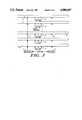
- FIG. 1is a general block diagram illustrating the memory system and associated control
- FIGS. 2A and 2Btogether represent a circuit block diagram of the backplane area of the memory illustrating the address shifter and memory array;
- FIG. 3is a schematic diagram illustrating the array or slot codes along with the data and addressing to each memory board.
- FIGS. 4 and 5are related diagrams useful in explaining the address shifting concepts of the present invention.
- the addressing scheme of the present inventionrelies upon a shift of addresses based upon the size of the largest capacity memory of all the memory arrays.
- the decodeis set based upon the size of the largest capacity array.
- the decodeis changed by changing the significance of the address lines sent to the backplane area through a shifter.
- FIG. 1for an illustration of the general system including a plurality of memory arrays 10, a memory controller 20, and also illustrated in FIG. 1, a central processing unit 30.
- the address shifter 25shifts the addresses presented from the CPU 30 to the backplane area 28 in accordance with a control signal as will all be described in further detail hereinafter.
- the control signalis established by determination of the largest capacity memory array.
- FIG. 1also illustrates connectors at C such as between the backplane area 28 and the memory controller 20 as well as connectors at the backplane area 28 into which the memory arrays 10 respectively connect.
- the memory arrays 10are typically referred to as memory boards and are furthermore referred to as being accommodated in memory slots in which the boards plug into connectors at the backplane area 28.
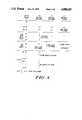
- FIG. 3illustrates a schematic illustration of the memory boards 10.
- FIG. 3also illustrates the address bus at 12 and the data bus at 14.
- the address lines as well as the data linescouple to all of the boards as schematically illustrated in FIG. 3 by the respective address and data lines 13 and 15.
- FIG. 3illustrates this as a single line for the sake of simplicity. However, it is understood that the address and data lines are actually comprised of multiple bit lines so as to provide the required number of address bits and data bits.
- This connectorhas, in the embodiment disclosed herein, three terminals identified at 16 in FIG. 3 for providing a slot or array code. Because there are eight boards 3 bits are required for providing a code representative of the particular board. Upon the plugging in of a memory array board, the particular code is accessible directly at that board. Representative boards are illustrated in FIG. 3. These codes may be established in a simple manner by the use of appropriate biasing resistors and logic voltage levels. With respect to the slot or array code 16 in FIG. 3 also refer to FIG. 2A wherein the code is illustrated as coupling to a comparator 18 to be described in further detail hereinafter.
- FIGS. 2A and 2Bfor an illustration of further details of the memory arrays as well as further details of the address shifter 25 and the backplane area 28.
- the backplane area 28there is illustrated the series of address lines, referred to bussed address lines BAL0-BAL26.
- FIG. 2Ashows the address lines BAL21-BAL26 while FIG. 2B shows the address lines BAL0-BAL20.
- FIGS. 2A and 2Bonly a single memory array 10 is illustrated. However, it is understood that a plurality of such arrays, as illustrated in FIG. 1, receive their addressing signals from the backplane area 28. Furthermore, associated with each memory board is a comparator such as the comparator 18 shown in FIG. 2A as well as a bank decoder 22 as also illustrated in FIG. 2A. Thus, associated with each memory array 10 is a comparator, the output of which provides the board select signal. Also, associated with each memory array 10 is the decoder 22 that provides the decode for the particular memory array bank.
- the memory array 10is illustrated as comprised of four separate random acccess memories referred to herein as four separate banks 10A-10D.
- Each of the memory banks 10A-10Dprovides two megabyte of storage.
- Each of the memory banksis a group of dynamic RAM's arranged to provide a word 8 bytes wide by 265K words.
- Each of these dynamic RAM'sin addition to being 8 bytes wide has each byte comprised of 8 bits thus providing the total of 2 MB of storage capacity.
- the addresses BAL0-BAL2provide three bits of address for byte selection. This selects between the 8 bytes of each ram.
- the addresses BAL3-BAL11These 9 bits are for row address selection.
- the addresses BAL12-BAL20These 9 bits are for column address selection.
- FIG. 4illustrates the addresses BAL0-BAL20 for providing byte selection along with row and column selection. This leaves the higher order addresses to decode which of the banks of memory are to be accessed on the board and to also decode which board or array to select in the backplane. For a 4 MB memory board, only one address is needed to decode 1 of 2 banks and if there is an 8 slot backplane, the next three higher addresses are compared to the binary slot or array code number to decode which array to address. This is also illustrated in FIG. 4.
- bussed address lines BAL21 and BAL22are the bits used for additional column and row addressing as illustrated in FIG. 4.
- FIG. 4also illustrates the bussed address lines BAL23, BAL24 and BAL25 as being the three bits for slot decode. This applies across the board for all capacity memory arrays. It is furthermore noted in FIG. 4 that for the 16 MB array the bussed address line BAL26 is used for the bank decode for 1 out of 2 banks. It is noted that for the 16 MB array 1 MB RAMs are used thus requiring only two banks for completing the full 16 MB capacity.
- the operation of the address shifter 25is controlled in accordance with the largest capacity memory that is employed. If the largest array in the system is a 4 MB array then the memory controller presents the CPU addresses to the backplane area 28 as illustrated in FIG. 5 at column (a).
- the address shifter 25, however,can be controlled to change the addresses presented to the backplane address lines (BAL) to that illustrated in FIG. 5 in columns (b) and (c). These columns respectively represent the 8 MB and 16 MB decodes and give the CPU addresses presented to the backplane bussed address lines. Note in FIG. 5 that these addresses are the same as presented at the inputs to the address shifter 25.
- the selection meansis set at the time of manufacture. This is illustrated in FIG. 2A by the jumper J that may be used to bridge across the different terminals illustrated, namely terminals J1-J3 for coupling signals by way of network 32 to control hardware or software as illustrated at 34. It is noted that from the control box 34 there are two control lines C1 and C2 that couple to the address shifter.
- the address shifter 25is implemented by a multiplexer 36 in which the control of signals passed through the multiplexer is by means of signals on lines C1 and C2. These are binary signals that may be either "1" or "0". This provides for four decoded conditions of the multiplexer 36.
- the following tablealso provides the megabyte decode boundaries.
- the multiplexer 36 in the embodiment disclosed in FIG. 2Ahas five segments, 36A-36E. Each of these segments has four inputs for the four different conditions imposed at the control lines C1 and C2, and has one single output.
- the output lines from the five segments 36A-36Ecouple to the backplane bussed address lines BAL22-BAL26. It is noted that CPU addresses are coupled to only three of the four inputs of each segment. Thus, in the embodiment of the multiplexer depicted in FIG. 2A this is providing for decoding of only three memory capacity decode conditions.
- FIG. 5illustrates the manner in which the address is sent out on the bussed address lines to the arrays can be changed.
- the signals coupled to the bussed address lines BAL23-BAL25are shifted depending upon whether it is a 4 megabyte decode boundary, an 8 megabyte decode boundary or a 16 megabyte decode boundary.
- addresses A22-A24apply for the 4 megabyte decode
- addresses A23-A25apply for the 8 megabyte decode
- addresses A24-A26apply for the 16 megabyte decode.
- the bus address line signals from positions BAL23-BAL26couple to one side of the comparator Q.
- the signal from address line BAL22couples by way of coupling means 38 to either the comparator 18 or the 2 input decoder 22.
- the coupling means 38 illustrated in FIG. 2Ais comprised of 2 pairs of jumpers identified in FIG. 2A as jumpers JA and jumpers JB.
- the jumpers JAare installed on a 4 MB board while the jumpers JB are installed in a 8 MB board.
- the multiplexer 36is illustrated with three sets of inputs, the circuitry illustrated in FIG. 2A is for handling only 4 MB and 8 MB decodes. Additional logic circuitry is required but is not described in FIG. 2A in connection with the 16 MB decode.
- the 16 MB decoderequires that the lines BAL21 and BAL22 couple to the memory board and thus additional logic is required to carry this out. This logic is not specifically set forth in FIG. 2A. However, FIG. 2A does completely describe the operation with respect to the 4 MB and 8 MB decodes.
- each of the boardshas the jumpers JA installed. This means that the signal from the address line BAL22 couples directly to the comparator 18.
- the other jumper JAgrounds one of the inputs to the decoder 22 and thus the decoder 22 only responds to address signals from address line BAL21. This is the case on a 4 MB decode boundary as illustrated in FIG. 5 at column (a).
- the CPU address A26is "0" and the signal from line BAL22 is essentially compared with the 0 input to the other side of the comparator at line 41.
- Next into the comparatorare the signals from lines BAL23-BAL25.
- comparator 18When the CPU presents an address with the code that corresponds to the slot code, then there is a comparison detected at comparator 18 providing an output signal identified in FIG. 2A as the board or array select signal. This signal couples by way of line 43 to enable the bank decoder 22. The signal also can couple to additional circuitry on the memory board such as for enabling data driven out of the memory back to the CPU. Also, the output from the comparator 18 includes a signal on line 44 that is coupled back to the CPU to indicate to the CPU that for the particular address just presented, there is in fact a board selection indicating that this is in fact a valid address.
- the JB jumpersare installed rather than the JA jumpers.
- the lines BAL21 and BAL22couple directly to the two inputs to the decoder 22. This is thus providing as indicated in FIG. 4, a bank decode of 1 out of 4 banks which is the decode for an 8 MB array. Recall that the 8 MB array has 4 banks rather than 2.
- the other jumper JBgrounds the line 47 which is the lowest input on the Q side of the comparator 18.
- the address inputs to the comparator 18 for memory array decodingincude the CPU address signals A23-A25 coupled from the bussed address lines BAL23-BAL25 to the comparator 18. Also, there is the CPU address A26 coupled by way of bussed address line BAL26 to the final input of the comparator 18 on the Q side thereof.
- the address line signals BAL21 and BAL22would couple to the memory array to provide a total of 10 column and rows select addresses.
- the CPU addresses A24-A26then function as the array select signals coupling to the comparator 18.
- the CPU address A23is used for bank decoding and would be coupled by logic circuitry to the bank decoder 22.
- the circuitryoperates so as to check the appropriate addresses to respond to only 4 MB worth of address.
- the 4 MB boarditself has the jumpers JA installed rather than the jumpers JB.
- the jumpers JAare installed meaning that the bank decoder 22 has only one active input from the address line BAL21.
- the address line BAL22couples to the decoder 47.
- the CPUcan send address signals on an initialization of the system to test the availability of memory spaces on a board-by-board basis.
- any address signals coupled in which the signal on line BAL22 is a "1"will indicate that no board is selected.
- This signalis coupled back to the CPU by way of line 44 to indicate essentially an address failure; meaning that for this particular address tested, there is no storage available.
- This storageis not available because on the 8 megabyte decode there is only a 4 megabyte board installed and thus this indicates to the CPU immediately that there are holes at this address space.
- the CPUcan test the memory arrays by writing to an address and then reading from the same address. If the read information does not correspond to the written information then this also is an indication to the CPU that this is an unusable address. Thus, in this way the CPU can interrogate the availability of memory space.
- the bank decoder 22it is illustrated in FIG. 2A as having four outputs. However, it is understood that when only one of the inputs to the decoder is active then there is only a selection between two of the four outputs. For an 8 MB array all four lines are active so that 1 of the 4 banks can be selected such as 1 of the 4 banks 10A-10C in FIG. 2B. For a 4 MB memory array, then only two of the outputs are active selecting 1 of only 2 of the banks of the array.
- the bank enables signals illustrated in FIG. 2Amay couple to additional memory circuitry not described herein. For example, the bank enable signals may be used at logic gates to enable memory timing signals such as the standard signals CAS and/or RAS for column and row address selection.
- each of the memory arraysmay comprise only a single memory bank.
- the bank decodersuch as decoder 22, shown in FIG. 2A of the present application is not needed.
Landscapes
- Engineering & Computer Science (AREA)
- Theoretical Computer Science (AREA)
- Physics & Mathematics (AREA)
- General Engineering & Computer Science (AREA)
- General Physics & Mathematics (AREA)
- Dram (AREA)
- Executing Machine-Instructions (AREA)
- Memory System (AREA)
Abstract
Description
TABLE 1 ______________________________________ JUMPERS C1 C2 DECODE ______________________________________None 0 0 4MB J1 0 1 8MB J2 1 0 16MB J3 1 1 32 MB ______________________________________
Claims (32)
Priority Applications (5)
| Application Number | Priority Date | Filing Date | Title |
|---|---|---|---|
| US07/046,456US4888687A (en) | 1987-05-04 | 1987-05-04 | Memory control system |
| AU14187/88AAU612636B2 (en) | 1987-05-04 | 1988-04-05 | Memory control system |
| CA000564206ACA1305562C (en) | 1987-05-04 | 1988-04-14 | Memory control system |
| JP63098025AJPS63285650A (en) | 1987-05-04 | 1988-04-20 | System and method for controlling memory address signal |
| EP19880106592EP0289899A3 (en) | 1987-05-04 | 1988-04-25 | Memory control system |
Applications Claiming Priority (1)
| Application Number | Priority Date | Filing Date | Title |
|---|---|---|---|
| US07/046,456US4888687A (en) | 1987-05-04 | 1987-05-04 | Memory control system |
Publications (1)
| Publication Number | Publication Date |
|---|---|
| US4888687Atrue US4888687A (en) | 1989-12-19 |
Family
ID=21943555
Family Applications (1)
| Application Number | Title | Priority Date | Filing Date |
|---|---|---|---|
| US07/046,456Expired - Fee RelatedUS4888687A (en) | 1987-05-04 | 1987-05-04 | Memory control system |
Country Status (5)
| Country | Link |
|---|---|
| US (1) | US4888687A (en) |
| EP (1) | EP0289899A3 (en) |
| JP (1) | JPS63285650A (en) |
| AU (1) | AU612636B2 (en) |
| CA (1) | CA1305562C (en) |
Cited By (42)
| Publication number | Priority date | Publication date | Assignee | Title |
|---|---|---|---|---|
| US5159676A (en)* | 1988-12-05 | 1992-10-27 | Micron Technology, Inc. | Semi-smart DRAM controller IC to provide a pseudo-cache mode of operation using standard page mode draws |
| US5220791A (en)* | 1992-06-01 | 1993-06-22 | Antonio Bulzomi | Heat resistant work shoe |
| US5237672A (en)* | 1989-07-28 | 1993-08-17 | Texas Instruments Incorporated | Dynamically adaptable memory controller for various size memories |
| US5386531A (en)* | 1991-05-15 | 1995-01-31 | International Business Machines Corporation | Computer system accelerator for multi-word cross-boundary storage access |
| US5488708A (en)* | 1990-03-05 | 1996-01-30 | Canon Kabushiki Kaisha | Memory management in an image processing apparatus with detachable memory |
| US5761478A (en)* | 1994-12-12 | 1998-06-02 | Texas Instruments Incorporated | Programmable memory interface for efficient transfer of different size data |
| US5835926A (en)* | 1992-12-15 | 1998-11-10 | Siemens Business Communication Systems, Inc. | Multiple memory addressing using adjustable chip select |
| US6512970B1 (en)* | 1997-08-14 | 2003-01-28 | Bayerische Motoren Werke Aktiengesellschaft | Electronic control device for controlling autonomously controllable assemblies |
| US20030221045A1 (en)* | 2002-05-22 | 2003-11-27 | Lsi Logic Corporation | DSP memory bank rotation |
| US20100020585A1 (en)* | 2005-09-02 | 2010-01-28 | Rajan Suresh N | Methods and apparatus of stacking drams |
| US7730338B2 (en) | 2006-07-31 | 2010-06-01 | Google Inc. | Interface circuit system and method for autonomously performing power management operations in conjunction with a plurality of memory circuits |
| US7761724B2 (en) | 2006-07-31 | 2010-07-20 | Google Inc. | Interface circuit system and method for performing power management operations in conjunction with only a portion of a memory circuit |
| US7990746B2 (en) | 2005-06-24 | 2011-08-02 | Google Inc. | Method and circuit for configuring memory core integrated circuit dies with memory interface integrated circuit dies |
| US8041881B2 (en) | 2006-07-31 | 2011-10-18 | Google Inc. | Memory device with emulated characteristics |
| US8055833B2 (en) | 2006-10-05 | 2011-11-08 | Google Inc. | System and method for increasing capacity, performance, and flexibility of flash storage |
| US8060774B2 (en) | 2005-06-24 | 2011-11-15 | Google Inc. | Memory systems and memory modules |
| US8077535B2 (en) | 2006-07-31 | 2011-12-13 | Google Inc. | Memory refresh apparatus and method |
| US8081474B1 (en) | 2007-12-18 | 2011-12-20 | Google Inc. | Embossed heat spreader |
| US8080874B1 (en) | 2007-09-14 | 2011-12-20 | Google Inc. | Providing additional space between an integrated circuit and a circuit board for positioning a component therebetween |
| US8089795B2 (en) | 2006-02-09 | 2012-01-03 | Google Inc. | Memory module with memory stack and interface with enhanced capabilities |
| US8090897B2 (en) | 2006-07-31 | 2012-01-03 | Google Inc. | System and method for simulating an aspect of a memory circuit |
| US8111566B1 (en) | 2007-11-16 | 2012-02-07 | Google, Inc. | Optimal channel design for memory devices for providing a high-speed memory interface |
| US8130560B1 (en) | 2006-11-13 | 2012-03-06 | Google Inc. | Multi-rank partial width memory modules |
| US8154935B2 (en) | 2006-07-31 | 2012-04-10 | Google Inc. | Delaying a signal communicated from a system to at least one of a plurality of memory circuits |
| US8169233B2 (en) | 2009-06-09 | 2012-05-01 | Google Inc. | Programming of DIMM termination resistance values |
| US8209479B2 (en) | 2007-07-18 | 2012-06-26 | Google Inc. | Memory circuit system and method |
| US8244971B2 (en) | 2006-07-31 | 2012-08-14 | Google Inc. | Memory circuit system and method |
| US8280714B2 (en) | 2006-07-31 | 2012-10-02 | Google Inc. | Memory circuit simulation system and method with refresh capabilities |
| US8327104B2 (en) | 2006-07-31 | 2012-12-04 | Google Inc. | Adjusting the timing of signals associated with a memory system |
| US8335894B1 (en) | 2008-07-25 | 2012-12-18 | Google Inc. | Configurable memory system with interface circuit |
| US8386722B1 (en) | 2008-06-23 | 2013-02-26 | Google Inc. | Stacked DIMM memory interface |
| US8397013B1 (en) | 2006-10-05 | 2013-03-12 | Google Inc. | Hybrid memory module |
| US8438328B2 (en) | 2008-02-21 | 2013-05-07 | Google Inc. | Emulation of abstracted DIMMs using abstracted DRAMs |
| US8566516B2 (en) | 2006-07-31 | 2013-10-22 | Google Inc. | Refresh management of memory modules |
| US8796830B1 (en) | 2006-09-01 | 2014-08-05 | Google Inc. | Stackable low-profile lead frame package |
| US8949519B2 (en) | 2005-06-24 | 2015-02-03 | Google Inc. | Simulating a memory circuit |
| US8972673B2 (en) | 2006-07-31 | 2015-03-03 | Google Inc. | Power management of memory circuits by virtual memory simulation |
| US9171585B2 (en) | 2005-06-24 | 2015-10-27 | Google Inc. | Configurable memory circuit system and method |
| US9507739B2 (en) | 2005-06-24 | 2016-11-29 | Google Inc. | Configurable memory circuit system and method |
| US9542352B2 (en) | 2006-02-09 | 2017-01-10 | Google Inc. | System and method for reducing command scheduling constraints of memory circuits |
| US9632929B2 (en)* | 2006-02-09 | 2017-04-25 | Google Inc. | Translating an address associated with a command communicated between a system and memory circuits |
| US10013371B2 (en) | 2005-06-24 | 2018-07-03 | Google Llc | Configurable memory circuit system and method |
Families Citing this family (3)
| Publication number | Priority date | Publication date | Assignee | Title |
|---|---|---|---|---|
| GB2232511B (en)* | 1989-05-19 | 1993-08-25 | Research Machines Ltd | Self configuring memory system |
| KR910008413B1 (en)* | 1989-07-21 | 1991-10-15 | 삼성전자 주식회사 | Memory Capacity Expansion Unit |
| DE59610672D1 (en)* | 1995-12-29 | 2003-09-25 | Siemens Ag | Method and arrangement for converting memory addresses into memory control signals |
Citations (7)
| Publication number | Priority date | Publication date | Assignee | Title |
|---|---|---|---|---|
| US4234934A (en)* | 1978-11-30 | 1980-11-18 | Sperry Rand Corporation | Apparatus for scaling memory addresses |
| US4545010A (en)* | 1983-03-31 | 1985-10-01 | Honeywell Information Systems Inc. | Memory identification apparatus and method |
| US4654787A (en)* | 1983-07-29 | 1987-03-31 | Hewlett-Packard Company | Apparatus for locating memory modules having different sizes within a memory space |
| US4675808A (en)* | 1983-08-08 | 1987-06-23 | American Telephone And Telegraph Company At&T Bell Laboratories | Multiplexed-address interface for addressing memories of various sizes |
| US4682283A (en)* | 1986-02-06 | 1987-07-21 | Rockwell International Corporation | Address range comparison system using multiplexer for detection of range identifier bits stored in dedicated RAM's |
| US4740916A (en)* | 1985-12-19 | 1988-04-26 | International Business Machines Corporation | Reconfigurable contiguous address space memory system including serially connected variable capacity memory modules and a split address bus |
| US4760522A (en)* | 1984-06-20 | 1988-07-26 | Weatherford James R | Intermixing of different capacity memory array units in a computer |
Family Cites Families (3)
| Publication number | Priority date | Publication date | Assignee | Title |
|---|---|---|---|---|
| US4281392A (en)* | 1979-05-01 | 1981-07-28 | Allen-Bradley Company | Memory circuit for programmable machines |
| NZ209664A (en)* | 1983-09-29 | 1987-05-29 | Tandem Computers Inc | Memory board address assignments: automatic reconfiguration |
| AU579725B2 (en)* | 1985-05-02 | 1988-12-08 | Digital Equipment Corporation | Arrangement for expanding memory capacity |
- 1987
- 1987-05-04USUS07/046,456patent/US4888687A/ennot_activeExpired - Fee Related
- 1988
- 1988-04-05AUAU14187/88Apatent/AU612636B2/ennot_activeCeased
- 1988-04-14CACA000564206Apatent/CA1305562C/ennot_activeExpired - Fee Related
- 1988-04-20JPJP63098025Apatent/JPS63285650A/enactivePending
- 1988-04-25EPEP19880106592patent/EP0289899A3/ennot_activeWithdrawn
Patent Citations (7)
| Publication number | Priority date | Publication date | Assignee | Title |
|---|---|---|---|---|
| US4234934A (en)* | 1978-11-30 | 1980-11-18 | Sperry Rand Corporation | Apparatus for scaling memory addresses |
| US4545010A (en)* | 1983-03-31 | 1985-10-01 | Honeywell Information Systems Inc. | Memory identification apparatus and method |
| US4654787A (en)* | 1983-07-29 | 1987-03-31 | Hewlett-Packard Company | Apparatus for locating memory modules having different sizes within a memory space |
| US4675808A (en)* | 1983-08-08 | 1987-06-23 | American Telephone And Telegraph Company At&T Bell Laboratories | Multiplexed-address interface for addressing memories of various sizes |
| US4760522A (en)* | 1984-06-20 | 1988-07-26 | Weatherford James R | Intermixing of different capacity memory array units in a computer |
| US4740916A (en)* | 1985-12-19 | 1988-04-26 | International Business Machines Corporation | Reconfigurable contiguous address space memory system including serially connected variable capacity memory modules and a split address bus |
| US4682283A (en)* | 1986-02-06 | 1987-07-21 | Rockwell International Corporation | Address range comparison system using multiplexer for detection of range identifier bits stored in dedicated RAM's |
Cited By (71)
| Publication number | Priority date | Publication date | Assignee | Title |
|---|---|---|---|---|
| US5159676A (en)* | 1988-12-05 | 1992-10-27 | Micron Technology, Inc. | Semi-smart DRAM controller IC to provide a pseudo-cache mode of operation using standard page mode draws |
| US5237672A (en)* | 1989-07-28 | 1993-08-17 | Texas Instruments Incorporated | Dynamically adaptable memory controller for various size memories |
| US5488708A (en)* | 1990-03-05 | 1996-01-30 | Canon Kabushiki Kaisha | Memory management in an image processing apparatus with detachable memory |
| US5386531A (en)* | 1991-05-15 | 1995-01-31 | International Business Machines Corporation | Computer system accelerator for multi-word cross-boundary storage access |
| US5220791A (en)* | 1992-06-01 | 1993-06-22 | Antonio Bulzomi | Heat resistant work shoe |
| US5835926A (en)* | 1992-12-15 | 1998-11-10 | Siemens Business Communication Systems, Inc. | Multiple memory addressing using adjustable chip select |
| US5761478A (en)* | 1994-12-12 | 1998-06-02 | Texas Instruments Incorporated | Programmable memory interface for efficient transfer of different size data |
| US6512970B1 (en)* | 1997-08-14 | 2003-01-28 | Bayerische Motoren Werke Aktiengesellschaft | Electronic control device for controlling autonomously controllable assemblies |
| US20030221045A1 (en)* | 2002-05-22 | 2003-11-27 | Lsi Logic Corporation | DSP memory bank rotation |
| US6895488B2 (en)* | 2002-05-22 | 2005-05-17 | Lsi Logic Corporation | DSP memory bank rotation |
| US7990746B2 (en) | 2005-06-24 | 2011-08-02 | Google Inc. | Method and circuit for configuring memory core integrated circuit dies with memory interface integrated circuit dies |
| US8060774B2 (en) | 2005-06-24 | 2011-11-15 | Google Inc. | Memory systems and memory modules |
| US8773937B2 (en) | 2005-06-24 | 2014-07-08 | Google Inc. | Memory refresh apparatus and method |
| US8615679B2 (en) | 2005-06-24 | 2013-12-24 | Google Inc. | Memory modules with reliability and serviceability functions |
| US8949519B2 (en) | 2005-06-24 | 2015-02-03 | Google Inc. | Simulating a memory circuit |
| US8386833B2 (en) | 2005-06-24 | 2013-02-26 | Google Inc. | Memory systems and memory modules |
| US9507739B2 (en) | 2005-06-24 | 2016-11-29 | Google Inc. | Configurable memory circuit system and method |
| US10013371B2 (en) | 2005-06-24 | 2018-07-03 | Google Llc | Configurable memory circuit system and method |
| US8359187B2 (en) | 2005-06-24 | 2013-01-22 | Google Inc. | Simulating a different number of memory circuit devices |
| US9171585B2 (en) | 2005-06-24 | 2015-10-27 | Google Inc. | Configurable memory circuit system and method |
| US20100020585A1 (en)* | 2005-09-02 | 2010-01-28 | Rajan Suresh N | Methods and apparatus of stacking drams |
| US8619452B2 (en) | 2005-09-02 | 2013-12-31 | Google Inc. | Methods and apparatus of stacking DRAMs |
| US8582339B2 (en) | 2005-09-02 | 2013-11-12 | Google Inc. | System including memory stacks |
| US8811065B2 (en) | 2005-09-02 | 2014-08-19 | Google Inc. | Performing error detection on DRAMs |
| US9727458B2 (en) | 2006-02-09 | 2017-08-08 | Google Inc. | Translating an address associated with a command communicated between a system and memory circuits |
| US8797779B2 (en) | 2006-02-09 | 2014-08-05 | Google Inc. | Memory module with memory stack and interface with enhanced capabilites |
| US9542353B2 (en) | 2006-02-09 | 2017-01-10 | Google Inc. | System and method for reducing command scheduling constraints of memory circuits |
| US9542352B2 (en) | 2006-02-09 | 2017-01-10 | Google Inc. | System and method for reducing command scheduling constraints of memory circuits |
| US8089795B2 (en) | 2006-02-09 | 2012-01-03 | Google Inc. | Memory module with memory stack and interface with enhanced capabilities |
| US9632929B2 (en)* | 2006-02-09 | 2017-04-25 | Google Inc. | Translating an address associated with a command communicated between a system and memory circuits |
| US8566556B2 (en) | 2006-02-09 | 2013-10-22 | Google Inc. | Memory module with memory stack and interface with enhanced capabilities |
| US8244971B2 (en) | 2006-07-31 | 2012-08-14 | Google Inc. | Memory circuit system and method |
| US8566516B2 (en) | 2006-07-31 | 2013-10-22 | Google Inc. | Refresh management of memory modules |
| US9047976B2 (en) | 2006-07-31 | 2015-06-02 | Google Inc. | Combined signal delay and power saving for use with a plurality of memory circuits |
| US8077535B2 (en) | 2006-07-31 | 2011-12-13 | Google Inc. | Memory refresh apparatus and method |
| US8972673B2 (en) | 2006-07-31 | 2015-03-03 | Google Inc. | Power management of memory circuits by virtual memory simulation |
| US8041881B2 (en) | 2006-07-31 | 2011-10-18 | Google Inc. | Memory device with emulated characteristics |
| US7761724B2 (en) | 2006-07-31 | 2010-07-20 | Google Inc. | Interface circuit system and method for performing power management operations in conjunction with only a portion of a memory circuit |
| US8868829B2 (en) | 2006-07-31 | 2014-10-21 | Google Inc. | Memory circuit system and method |
| US8327104B2 (en) | 2006-07-31 | 2012-12-04 | Google Inc. | Adjusting the timing of signals associated with a memory system |
| US8340953B2 (en) | 2006-07-31 | 2012-12-25 | Google, Inc. | Memory circuit simulation with power saving capabilities |
| US8280714B2 (en) | 2006-07-31 | 2012-10-02 | Google Inc. | Memory circuit simulation system and method with refresh capabilities |
| US8090897B2 (en) | 2006-07-31 | 2012-01-03 | Google Inc. | System and method for simulating an aspect of a memory circuit |
| US7730338B2 (en) | 2006-07-31 | 2010-06-01 | Google Inc. | Interface circuit system and method for autonomously performing power management operations in conjunction with a plurality of memory circuits |
| US8154935B2 (en) | 2006-07-31 | 2012-04-10 | Google Inc. | Delaying a signal communicated from a system to at least one of a plurality of memory circuits |
| US8631220B2 (en) | 2006-07-31 | 2014-01-14 | Google Inc. | Adjusting the timing of signals associated with a memory system |
| US8745321B2 (en) | 2006-07-31 | 2014-06-03 | Google Inc. | Simulating a memory standard |
| US8112266B2 (en) | 2006-07-31 | 2012-02-07 | Google Inc. | Apparatus for simulating an aspect of a memory circuit |
| US8796830B1 (en) | 2006-09-01 | 2014-08-05 | Google Inc. | Stackable low-profile lead frame package |
| US8370566B2 (en) | 2006-10-05 | 2013-02-05 | Google Inc. | System and method for increasing capacity, performance, and flexibility of flash storage |
| US8397013B1 (en) | 2006-10-05 | 2013-03-12 | Google Inc. | Hybrid memory module |
| US8751732B2 (en) | 2006-10-05 | 2014-06-10 | Google Inc. | System and method for increasing capacity, performance, and flexibility of flash storage |
| US8055833B2 (en) | 2006-10-05 | 2011-11-08 | Google Inc. | System and method for increasing capacity, performance, and flexibility of flash storage |
| US8977806B1 (en) | 2006-10-05 | 2015-03-10 | Google Inc. | Hybrid memory module |
| US8760936B1 (en) | 2006-11-13 | 2014-06-24 | Google Inc. | Multi-rank partial width memory modules |
| US8130560B1 (en) | 2006-11-13 | 2012-03-06 | Google Inc. | Multi-rank partial width memory modules |
| US8446781B1 (en) | 2006-11-13 | 2013-05-21 | Google Inc. | Multi-rank partial width memory modules |
| US8209479B2 (en) | 2007-07-18 | 2012-06-26 | Google Inc. | Memory circuit system and method |
| US8080874B1 (en) | 2007-09-14 | 2011-12-20 | Google Inc. | Providing additional space between an integrated circuit and a circuit board for positioning a component therebetween |
| US8675429B1 (en) | 2007-11-16 | 2014-03-18 | Google Inc. | Optimal channel design for memory devices for providing a high-speed memory interface |
| US8111566B1 (en) | 2007-11-16 | 2012-02-07 | Google, Inc. | Optimal channel design for memory devices for providing a high-speed memory interface |
| US8730670B1 (en) | 2007-12-18 | 2014-05-20 | Google Inc. | Embossed heat spreader |
| US8705240B1 (en) | 2007-12-18 | 2014-04-22 | Google Inc. | Embossed heat spreader |
| US8081474B1 (en) | 2007-12-18 | 2011-12-20 | Google Inc. | Embossed heat spreader |
| US8438328B2 (en) | 2008-02-21 | 2013-05-07 | Google Inc. | Emulation of abstracted DIMMs using abstracted DRAMs |
| US8631193B2 (en) | 2008-02-21 | 2014-01-14 | Google Inc. | Emulation of abstracted DIMMS using abstracted DRAMS |
| US8386722B1 (en) | 2008-06-23 | 2013-02-26 | Google Inc. | Stacked DIMM memory interface |
| US8762675B2 (en) | 2008-06-23 | 2014-06-24 | Google Inc. | Memory system for synchronous data transmission |
| US8819356B2 (en) | 2008-07-25 | 2014-08-26 | Google Inc. | Configurable multirank memory system with interface circuit |
| US8335894B1 (en) | 2008-07-25 | 2012-12-18 | Google Inc. | Configurable memory system with interface circuit |
| US8169233B2 (en) | 2009-06-09 | 2012-05-01 | Google Inc. | Programming of DIMM termination resistance values |
Also Published As
| Publication number | Publication date |
|---|---|
| EP0289899A2 (en) | 1988-11-09 |
| AU1418788A (en) | 1988-11-10 |
| AU612636B2 (en) | 1991-07-18 |
| EP0289899A3 (en) | 1990-10-10 |
| JPS63285650A (en) | 1988-11-22 |
| CA1305562C (en) | 1992-07-21 |
Similar Documents
| Publication | Publication Date | Title |
|---|---|---|
| US4888687A (en) | Memory control system | |
| US4545010A (en) | Memory identification apparatus and method | |
| US4303993A (en) | Memory present apparatus | |
| EP0076629B1 (en) | Reconfigureable memory system | |
| US4951248A (en) | Self configuring memory system | |
| US4908789A (en) | Method and system for automatically assigning memory modules of different predetermined capacities to contiguous segments of a linear address range | |
| EP0108346B1 (en) | Memory reconfiguration method in a data processing system | |
| US5129069A (en) | Method and apparatus for automatic memory configuration by a computer | |
| CA2116985C (en) | Memory system | |
| US4319343A (en) | Programmable digital memory circuit | |
| US5848258A (en) | Memory bank addressing scheme | |
| US5278801A (en) | Flexible addressing for drams | |
| JP3634393B2 (en) | Apparatus for determining the configuration of a computer memory | |
| JPS6259820B2 (en) | ||
| US4523313A (en) | Partial defective chip memory support system | |
| US4485471A (en) | Method of memory reconfiguration for fault tolerant memory | |
| US5179686A (en) | Method for automatically detecting the size of a memory by performing a memory warp operation | |
| US6470417B1 (en) | Emulation of next generation DRAM technology | |
| US5577004A (en) | Memory system and method | |
| US4882700A (en) | Switched memory module | |
| US5630086A (en) | Apparatus systems and methods for controlling electronic memories | |
| JPH07254270A (en) | Method and apparatus for control of plurality of banks of dram element | |
| CA1209276A (en) | Microcomputer system employing program cartridges | |
| US5586300A (en) | Flexible addressing memory controller wherein multiple memory modules may be accessed according to comparison of configuration addresses | |
| EP0200198B1 (en) | An arrangement for expanding memory capacity |
Legal Events
| Date | Code | Title | Description |
|---|---|---|---|
| AS | Assignment | Owner name:PRIME COMPUTER, INC., PRIME PARK, NATICK, MA A COR Free format text:ASSIGNMENT OF ASSIGNORS INTEREST.;ASSIGNORS:ALLISON, ROBERT;LEFSKY, BRIAN;REEL/FRAME:004736/0609 Effective date:19870707 | |
| FEPP | Fee payment procedure | Free format text:PAYOR NUMBER ASSIGNED (ORIGINAL EVENT CODE: ASPN); ENTITY STATUS OF PATENT OWNER: LARGE ENTITY | |
| AS | Assignment | Owner name:CHEMICAL BANK (A NEW YORK BANKING CORPORATION), NE Free format text:SECURITY INTEREST;ASSIGNORS:DR HOLDINGS INC., A DE CORP.;DR ACQUISITION CORP., A CORP. OF DE;PRIME COMPUTER INC.;AND OTHERS;REEL/FRAME:005333/0131 Effective date:19900130 | |
| AS | Assignment | Owner name:CHEMICAL BANK, A NY CORP., NEW YORK Free format text:SECURITY INTEREST;ASSIGNOR:COMPUTERVISION CORPORATION, A CORP. OF DE;REEL/FRAME:006314/0077 Effective date:19920821 | |
| FPAY | Fee payment | Year of fee payment:4 | |
| AS | Assignment | Owner name:COMPUTERVISION CORPORATION, MASSACHUSETTS Free format text:ASSIGNMENT OF ASSIGNORS INTEREST;ASSIGNOR:PRIME COMPUTER, INC.;REEL/FRAME:006663/0565 Effective date:19920813 | |
| AS | Assignment | Owner name:BANKERS TRUST COMPANY, NEW YORK Free format text:ASSIGNMENT OF SECURITY INTEREST;ASSIGNOR:COMPUTERVISION CORPORATION;REEL/FRAME:007815/0912 Effective date:19951117 | |
| REMI | Maintenance fee reminder mailed | ||
| LAPS | Lapse for failure to pay maintenance fees | ||
| FP | Lapsed due to failure to pay maintenance fee | Effective date:19971224 | |
| AS | Assignment | Owner name:CHASE MANHATTAN BANK (F/K/A CHEMICAL BANK), AS COL Free format text:TERMINATION AND RELEASE OF ASSIGNMENT OF SECURITY INTEREST IN PATENTS;ASSIGNOR:COMPUTERVISION CORPORATION, A DELAWARE CORPORATION;REEL/FRAME:009178/0329 Effective date:19980417 | |
| AS | Assignment | Owner name:BANKERS TRUST COMPANY, AS COLLATERAL AGENT, NEW YO Free format text:TERMINATION AND RELEASE OF ASSIGNMENT OF SECURITY;ASSIGNOR:COMPUTERVISION CORPORATION, A DELAWARE CORP.;REEL/FRAME:009342/0885 Effective date:19980417 | |
| STCH | Information on status: patent discontinuation | Free format text:PATENT EXPIRED DUE TO NONPAYMENT OF MAINTENANCE FEES UNDER 37 CFR 1.362 |