US4885719A - Improved logic cell array using CMOS E2 PROM cells - Google Patents
Improved logic cell array using CMOS E2 PROM cellsDownload PDFInfo
- Publication number
- US4885719A US4885719AUS07/087,143US8714387AUS4885719AUS 4885719 AUS4885719 AUS 4885719AUS 8714387 AUS8714387 AUS 8714387AUS 4885719 AUS4885719 AUS 4885719A
- Authority
- US
- United States
- Prior art keywords
- floating gate
- programming
- common
- cell
- polycrystalline silicon
- Prior art date
- Legal status (The legal status is an assumption and is not a legal conclusion. Google has not performed a legal analysis and makes no representation as to the accuracy of the status listed.)
- Expired - Lifetime
Links
- 229910021420polycrystalline siliconInorganic materials0.000claimsabstractdescription14
- 238000002347injectionMethods0.000claimsdescription3
- 239000007924injectionSubstances0.000claimsdescription3
- 239000002210silicon-based materialSubstances0.000claims3
- 229920005591polysiliconPolymers0.000abstractdescription7
- 238000003491arrayMethods0.000description7
- 230000006870functionEffects0.000description4
- 238000009877renderingMethods0.000description4
- 239000003990capacitorSubstances0.000description3
- 230000009977dual effectEffects0.000description3
- 239000004065semiconductorSubstances0.000description3
- 230000003068static effectEffects0.000description3
- XUIMIQQOPSSXEZ-UHFFFAOYSA-NSiliconChemical compound[Si]XUIMIQQOPSSXEZ-UHFFFAOYSA-N0.000description2
- 238000010586diagramMethods0.000description2
- 230000010354integrationEffects0.000description2
- 239000011159matrix materialSubstances0.000description2
- 239000002184metalSubstances0.000description2
- 229910052751metalInorganic materials0.000description2
- 229910052710siliconInorganic materials0.000description2
- 239000010703siliconSubstances0.000description2
- 230000000295complement effectEffects0.000description1
- 229910044991metal oxideInorganic materials0.000description1
- 150000004706metal oxidesChemical class0.000description1
- 238000000034methodMethods0.000description1
- 230000004048modificationEffects0.000description1
- 238000012986modificationMethods0.000description1
- 230000008520organizationEffects0.000description1
- 230000008569processEffects0.000description1
- 230000000306recurrent effectEffects0.000description1
- 230000008672reprogrammingEffects0.000description1
- 230000005641tunnelingEffects0.000description1
Images

Classifications
- G—PHYSICS
- G11—INFORMATION STORAGE
- G11C—STATIC STORES
- G11C16/00—Erasable programmable read-only memories
- G11C16/02—Erasable programmable read-only memories electrically programmable
- G11C16/04—Erasable programmable read-only memories electrically programmable using variable threshold transistors, e.g. FAMOS
- G11C16/0408—Erasable programmable read-only memories electrically programmable using variable threshold transistors, e.g. FAMOS comprising cells containing floating gate transistors
- G11C16/0441—Erasable programmable read-only memories electrically programmable using variable threshold transistors, e.g. FAMOS comprising cells containing floating gate transistors comprising cells containing multiple floating gate devices, e.g. separate read-and-write FAMOS transistors with connected floating gates
- G11C16/045—Floating gate memory cells with both P and N channel memory transistors, usually sharing a common floating gate
- G—PHYSICS
- G11—INFORMATION STORAGE
- G11C—STATIC STORES
- G11C16/00—Erasable programmable read-only memories
- G11C16/02—Erasable programmable read-only memories electrically programmable
- G11C16/04—Erasable programmable read-only memories electrically programmable using variable threshold transistors, e.g. FAMOS
- G11C16/0408—Erasable programmable read-only memories electrically programmable using variable threshold transistors, e.g. FAMOS comprising cells containing floating gate transistors
- G11C16/0441—Erasable programmable read-only memories electrically programmable using variable threshold transistors, e.g. FAMOS comprising cells containing floating gate transistors comprising cells containing multiple floating gate devices, e.g. separate read-and-write FAMOS transistors with connected floating gates
- H—ELECTRICITY
- H10—SEMICONDUCTOR DEVICES; ELECTRIC SOLID-STATE DEVICES NOT OTHERWISE PROVIDED FOR
- H10B—ELECTRONIC MEMORY DEVICES
- H10B69/00—Erasable-and-programmable ROM [EPROM] devices not provided for in groups H10B41/00 - H10B63/00, e.g. ultraviolet erasable-and-programmable ROM [UVEPROM] devices
Definitions
- This inventionrelates generally to application-specific integated circuits (ASIC) and more particularly the invention relates to a logic cell array (LCA) ASIC.
- ASICapplication-specific integated circuits
- LCDAlogic cell array
- ASIC devicesare programmable integrated circuits which allow logic circuit designers speed and flexibility in designing logic arrays.
- Mask programmable gate arraysoffer the highest degree of integration and flexibility, but have high, non-recurrent costs and require lengthy turn-around times.
- Field-programmable devicessuch as programmable array logic (PAL's) and programmable logic arrays (PLA's), and logic cell arrays (LCA's) provide faster turn-around at lower cost. Hower, the PAL and PLA implement only lower levels of integration with limited architectural flexibility.
- the LCAis a reprogrammable device that implements complex digital logic functions and has logic capabilities equivalent to small arrays.
- the implementation of user logic inside the LCAis accomplished with writable memory (RAM) cells rather than dedicated integrated circuit masks (as with gate arrays) or programmable fuses (as with PAL's and PLA's).
- RAMwritable memory
- PAL's and PLA'sdedicated integrated circuit masks
- PAL's and PLA'sprogrammable fuses
- Interleaved between rows and columns of the configurable logic blocksare user-definable interconnection resources (wiring paths) which provide the means for routing signals between the configurable logic blocks.
- a RAMis used to directly implement combinational logic functions, instead of the typical AND/OR gating function found in PAL's and PLA's.
- input/output blocksArranged along the outside perimeter of the LCA die and surrounding the matrix of configurable logic blocks. From an architectural point of view the LCA closely resembles a gate array in its organization yet retains the features and advantages of field-programmable logic devices.
- Each cell of the conventional LCAconsists of six transistors which necessitates a considerable chip area for each cell. Further, the cell provides static memory and requires reprogramming upon loss of power.
- An object of the present inventionis an improved application-specific integrated circuit.
- Another object of the present inventionis a logic cell requiring reduced chip surface area.
- Yet another object of the present inventionis a memory cell structure for a logic cell which provides an active output (O or V cc ) without the necessity of auxiliary circuitry.
- a feature of the inventionis a CMOS E 2 PROM cell structure.
- each memory cell of an LCA in accordance with the inventionincludes a CMOS transistor pair connected between V cc and circuit ground.
- the output of the cellis taken at the common terminal of the transistor pair.
- the two transistorshave interconnected floating gates with programming means provided to selectively charge the floating gates for a "1" or "0" bit storage. Depending upon the stored bit, the output voltage from the cell will be Vcc or ground.
- the celldoes not consume any DC power with the output being either Vcc or ground.
- the programming meanscomprises capacitive means for applying a control gate voltage to the floating gate.
- the capacitor platescan comprise overlying polysilicon layers in a dual poly structure.
- a tunnel oxideseparates the floating gate from a charge tunnelling electrode.
- the charge tunnelling electrodeis connected to a programming voltage terminal through a transistor.
- the cell structureis useful not only in an ASIC application but in other applications such as a redundant back-up memory and as a programmable switch.
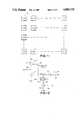
- FIG. 1is a functional block diagram of a logic cell array.
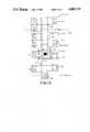
- FIG. 2is a schematic of a memory cell in accordance with the invention, useful in the logic cell array of FIG. 1.
- FIG. 3is a plan view of the layout of the cell of FIG. 2 in a semiconductor chip.
- FIG. 4is a schematic of an alternative embodiment of a memory cell in accordance with the invention.
- FIG. 5is a plan view of the layout of the cell of FIG. 4 in a semiconductor chip.
- FIG. 1is a schematic block diagram of a logic cell array.
- one commercially-available logic cell arraycomprises sixty-four configurable logic blocks (CLB) arranged in an eight-by-eight array as illustrated in FIG. 1.
- CLBconfigurable logic blocks
- Each of the configurable logic blocks 10 in FIG. 1consists of a combinational logic section with four general-purpose programming inputs, a storage element (flip-flop or latch) with a programmable clock input, and two programmable logic outputs.
- Each storage elementwhich can be either a D-type flip-flop or a gated transparent latch, includes a data input driven by the combinational logic function.
- the logic cell arraycommercially available from Xilinx Corporation utilizes a static memory cell consisting of six transistors, which necessarily require a considerable surface area on the integrated circuit. Further, the static cell loses data when power is lost and therefore must be reprogrammed.
- an improved memory cellthat requires at most three transistors.
- Two of the transistorscomprise complementary metal oxide silicon (CMOS) electrically erasable (E 2 ) transistors.
- CMOScomplementary metal oxide silicon
- E 2electrically erasable
- the p-channel transistor 20is connected to the +voltage source, V cc
- the n-channel transistor 22is connected to circuit ground.
- the output of the memory cellis taken at the common terminal 24 of the two transistors.
- the two CMOS transistorshave a common floating gate 26 which can be electrically programmed by the tunnelling of electrons through a tunnel oxide 28 separating the floating gates from a p+ programming electrode 30.
- Electrode 30is connected to a programming potential (PGM) 32 through an n-channel transistor 34.
- the gate of transistor 34is connected to a select gate (SG) terminal 36.
- the common floating gatesis coupled through capacitor 40 to a control gate (CG) electrode 42.
- the floating gatecan comprise a poly 1 layer
- the control gatecan comprise a poly 2 layer.
- the capacitor 40is formed where the poly 2 layer overlies the poly 1 layer.
- the control gate 42is raised to a programming voltage (V pp ) of 17 volts, the select gate is made positive (V cc or 17 volts) thereby rendering transistor 34 conductive, and the programming voltage (PGM) is tied to ground. Electrons from ground pass through transistor 34 and tunnel through the tunnel oxide 28 to the floating gate as attracted by the positive voltage of the control gate. The resulting negative charge on the floating gate causes the p-channel transistor 20 to conduct and the n-channel transistor 22 to not conduct, thereby applying V cc ("1") on the output.
- the voltage (CG) on the control gate 42is ground, a positive voltage is applied to the select gate (SG) rendering transistor 34 conductive, and the programming voltage (PGM) is made positive (e.g. 17 volts).
- the programming voltage (PGM)is made positive (e.g. 17 volts).
- the voltage on the poly 2 line (CG)will be 3 volts, and both SG and PGM will be grounded.
- FIG. 3is a plan view of the layout of the cell of FIG. 2 in a semiconductor chip using a conventional dual polysilicon layer process. Like elements have the same reference numerals.
- the p-channel transistor 20is formed in an n-well at the top of the cell, the n-channel transistor 22 is in the middle of the cell, and the terminals 24 of the two transistors are interconnected by a metal layer (not shown).
- the floating gate 26comprises a first polysilicon layer. Separate metal lines (not shown) are provided for V cc , V ss , and PGM.
- a buried n+ layeris provided under the floating gate and the tunneling area 30 to facilitate current injection to the floating gate.
- FIG. 4is an alternative embodiment of a memory cell similar to the cell of FIG. 2, and again like elements have the same reference numerals.
- logic 1'scan be selectively written instead of logic 0's as in FIG. 2.
- PGMgoes to 17 V
- logic 0'sare loaded in all the locations at the same time where the PGM signal is common.
- SGgoes to 18 V
- VCG17 V hence the selected device will have 17 V on CG.
- Thisenables the electrons from PGM (at 0 V) to tunnel to the floating gate, thus raising its threshold.
- PGM0 V
- FIG. 4The layout of FIG. 4 in silicon is shown in FIG. 5. Again, like elements have the same reference numerals.
- the described cells in accordance with the inventionare smaller in structure due to the reduced number of transistors. Further, no D.C. power is drawn in either the "1" or the "0" state.
- the cellhas applicability not only in a logic cell array but can be employed also as a redundant back-up memory or as a programmable switch.
Landscapes
- Engineering & Computer Science (AREA)
- Microelectronics & Electronic Packaging (AREA)
- Read Only Memory (AREA)
- Non-Volatile Memory (AREA)
Abstract
Description
______________________________________ MODE V-CG V-SG V-PGM ______________________________________ ERASE 17 V VCC 0 V (to a logic 1) or 17 V NORMAL 3 V 0 V 0 V (Read) WRITE 0 V 18 V 17 V (to a logic 0) ______________________________________
Claims (4)
Priority Applications (1)
| Application Number | Priority Date | Filing Date | Title |
|---|---|---|---|
| US07/087,143US4885719A (en) | 1987-08-19 | 1987-08-19 | Improved logic cell array using CMOS E2 PROM cells |
Applications Claiming Priority (1)
| Application Number | Priority Date | Filing Date | Title |
|---|---|---|---|
| US07/087,143US4885719A (en) | 1987-08-19 | 1987-08-19 | Improved logic cell array using CMOS E2 PROM cells |
Publications (1)
| Publication Number | Publication Date |
|---|---|
| US4885719Atrue US4885719A (en) | 1989-12-05 |
Family
ID=22203369
Family Applications (1)
| Application Number | Title | Priority Date | Filing Date |
|---|---|---|---|
| US07/087,143Expired - LifetimeUS4885719A (en) | 1987-08-19 | 1987-08-19 | Improved logic cell array using CMOS E2 PROM cells |
Country Status (1)
| Country | Link |
|---|---|
| US (1) | US4885719A (en) |
Cited By (55)
| Publication number | Priority date | Publication date | Assignee | Title |
|---|---|---|---|---|
| EP0431911A3 (en)* | 1989-12-07 | 1992-06-03 | Fujitsu Limited | Memory cell having floating gate and semiconductor memory using the same |
| US5126969A (en)* | 1989-08-09 | 1992-06-30 | Kawasaki Steel Corporation | Integrated circuit including non-volatile memory cell capable of temporarily holding information |
| US5247478A (en)* | 1992-03-06 | 1993-09-21 | Altera Corporation | Programmable transfer-devices |
| EP0515039A3 (en)* | 1991-05-10 | 1994-01-12 | Altera Corp | |
| WO1996021273A3 (en)* | 1995-01-06 | 1996-09-12 | Actel Corp | Two-transistor zero-power electrically-alterable non-volatile latch |
| US5587945A (en)* | 1995-11-06 | 1996-12-24 | Advanced Micro Devices, Inc. | CMOS EEPROM cell with tunneling window in the read path |
| US5594687A (en)* | 1995-04-21 | 1997-01-14 | Advanced Micro Devices, Inc. | Completely complementary MOS memory cell with tunneling through the NMOS and PMOS transistors during program and erase |
| WO1997002572A1 (en)* | 1995-07-03 | 1997-01-23 | Advanced Micro Devices, Inc. | Non-volatile memory cells using only positive charge to store data |
| US5615150A (en)* | 1995-11-02 | 1997-03-25 | Advanced Micro Devices, Inc. | Control gate-addressed CMOS non-volatile cell that programs through gates of CMOS transistors |
| WO1997019453A1 (en)* | 1995-11-17 | 1997-05-29 | Advanced Micro Devices, Inc. | Memory cell for a programmable logic device (pld) avoiding pumping programming voltage above an nmos threshold |
| US5646901A (en)* | 1996-03-26 | 1997-07-08 | Advanced Micro Devices, Inc. | CMOS memory cell with tunneling during program and erase through the NMOS and PMOS transistors and a pass gate separating the NMOS and PMOS transistors |
| US5754471A (en)* | 1995-06-06 | 1998-05-19 | Advanced Micro Devices, Inc. | Low power CMOS array for a PLD with program and erase using controlled avalanche injection |
| US5761116A (en)* | 1996-10-07 | 1998-06-02 | Advanced Micro Devices, Inc. | Vpp only scalable EEPROM memory cell having transistors with thin tunnel gate oxide |
| US5781033A (en)* | 1990-05-11 | 1998-07-14 | Actel Corporation | Logic module with configurable combinational and sequential blocks |
| US5796295A (en)* | 1995-04-21 | 1998-08-18 | Advanced Micro Devices, Inc. | Reference for CMOS memory cell having PMOS and NMOS transistors with a common floating gate |
| US5812450A (en)* | 1995-08-17 | 1998-09-22 | Altera Corporation | Nonvolatile SRAM cells and cell arrays |
| US5838606A (en)* | 1997-04-28 | 1998-11-17 | Mitsubishi Semiconductor America, Inc. | Three-transistor static storage cell |
| US5914904A (en)* | 1996-10-01 | 1999-06-22 | Altera Corporation | Compact electrically erasable memory cells and arrays |
| US5936426A (en)* | 1997-02-03 | 1999-08-10 | Actel Corporation | Logic function module for field programmable array |
| US5949710A (en)* | 1996-04-10 | 1999-09-07 | Altera Corporation | Programmable interconnect junction |
| US5959891A (en)* | 1996-08-16 | 1999-09-28 | Altera Corporation | Evaluation of memory cell characteristics |
| US5970005A (en)* | 1998-04-27 | 1999-10-19 | Ict, Inc. | Testing structure and method for high density PLDs which have flexible logic built-in blocks |
| US6005806A (en)* | 1996-03-14 | 1999-12-21 | Altera Corporation | Nonvolatile configuration cells and cell arrays |
| US6018476A (en)* | 1996-09-16 | 2000-01-25 | Altera Corporation | Nonvolatile configuration cells and cell arrays |
| WO2000038240A1 (en)* | 1998-12-21 | 2000-06-29 | Lattice Semiconductor Corporation | Floating gate memory cell structure with programming mechanism outside the read path |
| WO2000039856A1 (en)* | 1998-12-28 | 2000-07-06 | Lattice Semiconductor Corporation | Avalanche programmed floating gate memory cell structure with program element in polysilicon |
| US6144580A (en)* | 1998-12-11 | 2000-11-07 | Cypress Semiconductor Corp. | Non-volatile inverter latch |
| US6214666B1 (en) | 1998-12-18 | 2001-04-10 | Vantis Corporation | Method of forming a non-volatile memory device |
| US6215700B1 (en) | 1999-01-07 | 2001-04-10 | Vantis Corporation | PMOS avalanche programmed floating gate memory cell structure |
| US6236597B1 (en) | 1996-09-16 | 2001-05-22 | Altera Corporation | Nonvolatile memory cell with multiple gate oxide thicknesses |
| US6282123B1 (en) | 1998-12-21 | 2001-08-28 | Lattice Semiconductor Corporation | Method of fabricating, programming, and erasing a dual pocket two sided program/erase non-volatile memory cell |
| US6326663B1 (en) | 1999-03-26 | 2001-12-04 | Vantis Corporation | Avalanche injection EEPROM memory cell with P-type control gate |
| EP1217626A1 (en)* | 1993-03-17 | 2002-06-26 | Fujitsu Limited | Enhancement-mode NMOS transistor |
| US6424000B1 (en) | 1999-05-11 | 2002-07-23 | Vantis Corporation | Floating gate memory apparatus and method for selected programming thereof |
| US6489806B1 (en) | 2001-11-14 | 2002-12-03 | Lattice Semiconductor Corporation | Zero-power logic cell for use in programmable logic devices |
| US6512263B1 (en) | 2000-09-22 | 2003-01-28 | Sandisk Corporation | Non-volatile memory cell array having discontinuous source and drain diffusions contacted by continuous bit line conductors and methods of forming |
| US20030143793A1 (en)* | 2002-01-29 | 2003-07-31 | Andrew Horch | Method of preventing high Icc at start-up in zero-power EEPROM cells for PLD applications |
| US6611463B1 (en) | 2001-11-14 | 2003-08-26 | Lattice Semiconductor Corporation | Zero-power programmable memory cell |
| US6683477B1 (en) | 2000-11-02 | 2004-01-27 | Lattice Semiconductor Corporation | Memory cell |
| US6954381B2 (en)* | 1992-01-14 | 2005-10-11 | Sandisk Corporation | EEPROM with split gate source side injection with sidewall spacers |
| US20090147432A1 (en)* | 2007-12-07 | 2009-06-11 | Metamems Llc | Forming large planar structures from substrates using edge coulomb forces |
| US20090147434A1 (en)* | 2007-12-07 | 2009-06-11 | Metamems Llc | Using multiple coulomb islands to reduce voltage stress |
| US20090149038A1 (en)* | 2007-12-07 | 2009-06-11 | Metamems Llc | Forming edge metallic contacts and using coulomb forces to improve ohmic contact |
| US20090145229A1 (en)* | 2007-12-07 | 2009-06-11 | Metamems Llc | Decelerometer formed by levitating a substrate into equilibrium |
| US20090145631A1 (en)* | 2007-12-07 | 2009-06-11 | Metamems Llc | Reconfigurable system that exchanges substrates using coulomb forces to optimize a parameter |
| US20090147437A1 (en)* | 2007-12-07 | 2009-06-11 | Metamems Llc | Coulomb island and faraday shield used to create adjustable coulomb forces |
| US20090146890A1 (en)* | 2007-12-07 | 2009-06-11 | Metamems Llc | Using coulomb forces to form 3-d reconfigurable structures |
| US20090148932A1 (en)* | 2007-12-07 | 2009-06-11 | Metamems Llc | Using coulomb forces to study charateristics of fluids and biological samples |
| US20090147433A1 (en)* | 2007-12-07 | 2009-06-11 | Metamems Llc | Levitating substrate being charged by a non-volatile device and powered by a charged capacitor or bonding wire |
| US7646638B1 (en)* | 2007-09-06 | 2010-01-12 | National Semiconductor Corporation | Non-volatile memory cell that inhibits over-erasure and related method and memory array |
| US20100097776A1 (en)* | 2007-12-07 | 2010-04-22 | Lctank Llc | Assembling Stacked Substrates That Can Form 3-D Structures |
| US7859240B1 (en) | 2007-05-22 | 2010-12-28 | Cypress Semiconductor Corporation | Circuit and method for preventing reverse current flow into a voltage regulator from an output thereof |
| US20110235425A1 (en)* | 2010-03-25 | 2011-09-29 | Pavel Poplevine | Method of directly reading output voltage to determine data stored in a non-volatile memory cell |
| US20140252346A1 (en)* | 2010-01-20 | 2014-09-11 | Semiconductor Energy Laboratory Co., Ltd. | Semiconductor device |
| US10564698B2 (en) | 2016-08-19 | 2020-02-18 | Semiconductor Energy Laboratory Co., Ltd. | Method for controlling power supply in semiconductor device |
Citations (5)
| Publication number | Priority date | Publication date | Assignee | Title |
|---|---|---|---|---|
| US4053798A (en)* | 1975-02-20 | 1977-10-11 | Matsushita Electronics Corporation | Negative resistance device |
| US4228527A (en)* | 1978-02-22 | 1980-10-14 | Centre Electronique Horloger S.A. | Electrically reprogrammable non volatile memory |
| US4596938A (en)* | 1982-09-30 | 1986-06-24 | Rca Corporation | Electrically erasable programmable electronic circuits using programmable-threshold-voltage FET pairs |
| US4686558A (en)* | 1982-09-15 | 1987-08-11 | Itt Industries, Inc. | CMOS memory cell having an electrically floating storage gate |
| US4710900A (en)* | 1984-12-28 | 1987-12-01 | Nec Corporation | Non-volatile semiconductor memory device having an improved write circuit |
- 1987
- 1987-08-19USUS07/087,143patent/US4885719A/ennot_activeExpired - Lifetime
Patent Citations (5)
| Publication number | Priority date | Publication date | Assignee | Title |
|---|---|---|---|---|
| US4053798A (en)* | 1975-02-20 | 1977-10-11 | Matsushita Electronics Corporation | Negative resistance device |
| US4228527A (en)* | 1978-02-22 | 1980-10-14 | Centre Electronique Horloger S.A. | Electrically reprogrammable non volatile memory |
| US4686558A (en)* | 1982-09-15 | 1987-08-11 | Itt Industries, Inc. | CMOS memory cell having an electrically floating storage gate |
| US4596938A (en)* | 1982-09-30 | 1986-06-24 | Rca Corporation | Electrically erasable programmable electronic circuits using programmable-threshold-voltage FET pairs |
| US4710900A (en)* | 1984-12-28 | 1987-12-01 | Nec Corporation | Non-volatile semiconductor memory device having an improved write circuit |
Non-Patent Citations (2)
| Title |
|---|
| Landry, "Logic Cell Arrays: High Density, User Programmable ASICs", Technological Horizons, Mar. 1986. |
| Landry, Logic Cell Arrays: High Density, User Programmable ASICs , Technological Horizons, Mar. 1986.* |
Cited By (103)
| Publication number | Priority date | Publication date | Assignee | Title |
|---|---|---|---|---|
| US5126969A (en)* | 1989-08-09 | 1992-06-30 | Kawasaki Steel Corporation | Integrated circuit including non-volatile memory cell capable of temporarily holding information |
| US5404328A (en)* | 1989-12-07 | 1995-04-04 | Fujitsu Limited | Memory cell having floating gate and semiconductor memory using the same |
| EP0431911A3 (en)* | 1989-12-07 | 1992-06-03 | Fujitsu Limited | Memory cell having floating gate and semiconductor memory using the same |
| US5781033A (en)* | 1990-05-11 | 1998-07-14 | Actel Corporation | Logic module with configurable combinational and sequential blocks |
| EP0515039A3 (en)* | 1991-05-10 | 1994-01-12 | Altera Corp | |
| US6954381B2 (en)* | 1992-01-14 | 2005-10-11 | Sandisk Corporation | EEPROM with split gate source side injection with sidewall spacers |
| US5247478A (en)* | 1992-03-06 | 1993-09-21 | Altera Corporation | Programmable transfer-devices |
| EP1217626A1 (en)* | 1993-03-17 | 2002-06-26 | Fujitsu Limited | Enhancement-mode NMOS transistor |
| WO1996021273A3 (en)* | 1995-01-06 | 1996-09-12 | Actel Corp | Two-transistor zero-power electrically-alterable non-volatile latch |
| US5587603A (en)* | 1995-01-06 | 1996-12-24 | Actel Corporation | Two-transistor zero-power electrically-alterable non-volatile latch |
| US5596524A (en)* | 1995-04-21 | 1997-01-21 | Advanced Micro Devices, Inc. | CMOS memory cell with gate oxide of both NMOS and PMOS transistors as tunneling window for program and erase |
| US5796295A (en)* | 1995-04-21 | 1998-08-18 | Advanced Micro Devices, Inc. | Reference for CMOS memory cell having PMOS and NMOS transistors with a common floating gate |
| US5594687A (en)* | 1995-04-21 | 1997-01-14 | Advanced Micro Devices, Inc. | Completely complementary MOS memory cell with tunneling through the NMOS and PMOS transistors during program and erase |
| US5754471A (en)* | 1995-06-06 | 1998-05-19 | Advanced Micro Devices, Inc. | Low power CMOS array for a PLD with program and erase using controlled avalanche injection |
| WO1997002572A1 (en)* | 1995-07-03 | 1997-01-23 | Advanced Micro Devices, Inc. | Non-volatile memory cells using only positive charge to store data |
| US5812450A (en)* | 1995-08-17 | 1998-09-22 | Altera Corporation | Nonvolatile SRAM cells and cell arrays |
| WO1997016886A3 (en)* | 1995-11-02 | 1997-11-13 | Advanced Micro Devices Inc | Control gate-addressed cmos non-volatile memory cell that programs through gates of cmos transistors |
| US5615150A (en)* | 1995-11-02 | 1997-03-25 | Advanced Micro Devices, Inc. | Control gate-addressed CMOS non-volatile cell that programs through gates of CMOS transistors |
| US5587945A (en)* | 1995-11-06 | 1996-12-24 | Advanced Micro Devices, Inc. | CMOS EEPROM cell with tunneling window in the read path |
| US5666309A (en)* | 1995-11-17 | 1997-09-09 | Advanced Micro Devices, Inc. | Memory cell for a programmable logic device (PLD) avoiding pumping programming voltage above an NMOS threshold |
| WO1997019453A1 (en)* | 1995-11-17 | 1997-05-29 | Advanced Micro Devices, Inc. | Memory cell for a programmable logic device (pld) avoiding pumping programming voltage above an nmos threshold |
| US6226201B1 (en) | 1996-03-14 | 2001-05-01 | Altera Corporation | Techniques to configure nonvolatile cells and cell arrays |
| US6295230B1 (en) | 1996-03-14 | 2001-09-25 | Altera Coporation | Nonvolatile configuration cells and cell arrays |
| US6366498B1 (en) | 1996-03-14 | 2002-04-02 | Altera Corporation | Nonvolatile configuration cells and cell arrays |
| US6052309A (en)* | 1996-03-14 | 2000-04-18 | Altera Corporation | Nonvolatile configuration cells and cell arrays |
| US6532170B1 (en) | 1996-03-14 | 2003-03-11 | Altera Corporation | Nonvolatile configuration cells and cell arrays |
| US6005806A (en)* | 1996-03-14 | 1999-12-21 | Altera Corporation | Nonvolatile configuration cells and cell arrays |
| US5646901A (en)* | 1996-03-26 | 1997-07-08 | Advanced Micro Devices, Inc. | CMOS memory cell with tunneling during program and erase through the NMOS and PMOS transistors and a pass gate separating the NMOS and PMOS transistors |
| US6573138B1 (en) | 1996-04-10 | 2003-06-03 | Altera Corporation | Nonvolatile memory cell with low doping region |
| US5949710A (en)* | 1996-04-10 | 1999-09-07 | Altera Corporation | Programmable interconnect junction |
| US20030197218A1 (en)* | 1996-04-10 | 2003-10-23 | Altera Corporation | Nonvolatile memory cell with low doping region |
| US6828620B2 (en) | 1996-04-10 | 2004-12-07 | Altera Corporation | Nonvolatile memory cell with low doping region |
| US6122209A (en)* | 1996-04-10 | 2000-09-19 | Altera Corporation | Method of margin testing programmable interconnect cell |
| US6031763A (en)* | 1996-08-16 | 2000-02-29 | Altera Corporation | Evaluation of memory cell characteristics |
| US5959891A (en)* | 1996-08-16 | 1999-09-28 | Altera Corporation | Evaluation of memory cell characteristics |
| US6282122B1 (en) | 1996-08-16 | 2001-08-28 | Altera Corporation | Evaluation of memory cell characteristics |
| US6442073B1 (en) | 1996-09-16 | 2002-08-27 | Altera Corporation | Nonvolatile memory cell with multiple gate oxide thicknesses |
| US6078521A (en)* | 1996-09-16 | 2000-06-20 | Altera Corporation | Nonvolatile configuration cells and cell arrays |
| US6236597B1 (en) | 1996-09-16 | 2001-05-22 | Altera Corporation | Nonvolatile memory cell with multiple gate oxide thicknesses |
| US6018476A (en)* | 1996-09-16 | 2000-01-25 | Altera Corporation | Nonvolatile configuration cells and cell arrays |
| US6243296B1 (en) | 1996-10-01 | 2001-06-05 | Altera Corporation | Compact electrically erasable memory cells and arrays |
| US5914904A (en)* | 1996-10-01 | 1999-06-22 | Altera Corporation | Compact electrically erasable memory cells and arrays |
| US5761116A (en)* | 1996-10-07 | 1998-06-02 | Advanced Micro Devices, Inc. | Vpp only scalable EEPROM memory cell having transistors with thin tunnel gate oxide |
| US5936426A (en)* | 1997-02-03 | 1999-08-10 | Actel Corporation | Logic function module for field programmable array |
| US5838606A (en)* | 1997-04-28 | 1998-11-17 | Mitsubishi Semiconductor America, Inc. | Three-transistor static storage cell |
| US5970005A (en)* | 1998-04-27 | 1999-10-19 | Ict, Inc. | Testing structure and method for high density PLDs which have flexible logic built-in blocks |
| US6144580A (en)* | 1998-12-11 | 2000-11-07 | Cypress Semiconductor Corp. | Non-volatile inverter latch |
| US6349055B1 (en) | 1998-12-11 | 2002-02-19 | Cypress Semiconductor Corp. | Non-volatile inverter latch |
| US6214666B1 (en) | 1998-12-18 | 2001-04-10 | Vantis Corporation | Method of forming a non-volatile memory device |
| US6282123B1 (en) | 1998-12-21 | 2001-08-28 | Lattice Semiconductor Corporation | Method of fabricating, programming, and erasing a dual pocket two sided program/erase non-volatile memory cell |
| WO2000038240A1 (en)* | 1998-12-21 | 2000-06-29 | Lattice Semiconductor Corporation | Floating gate memory cell structure with programming mechanism outside the read path |
| US6232631B1 (en) | 1998-12-21 | 2001-05-15 | Vantis Corporation | Floating gate memory cell structure with programming mechanism outside the read path |
| WO2000039856A1 (en)* | 1998-12-28 | 2000-07-06 | Lattice Semiconductor Corporation | Avalanche programmed floating gate memory cell structure with program element in polysilicon |
| US6294809B1 (en) | 1998-12-28 | 2001-09-25 | Vantis Corporation | Avalanche programmed floating gate memory cell structure with program element in polysilicon |
| US6215700B1 (en) | 1999-01-07 | 2001-04-10 | Vantis Corporation | PMOS avalanche programmed floating gate memory cell structure |
| US6326663B1 (en) | 1999-03-26 | 2001-12-04 | Vantis Corporation | Avalanche injection EEPROM memory cell with P-type control gate |
| US6424000B1 (en) | 1999-05-11 | 2002-07-23 | Vantis Corporation | Floating gate memory apparatus and method for selected programming thereof |
| US7541237B2 (en) | 2000-09-22 | 2009-06-02 | Sandisk Corporation | Non-volatile memory cell array having discontinuous source and drain diffusions contacted by continuous bit line conductors and methods of forming |
| US6512263B1 (en) | 2000-09-22 | 2003-01-28 | Sandisk Corporation | Non-volatile memory cell array having discontinuous source and drain diffusions contacted by continuous bit line conductors and methods of forming |
| US20080026528A1 (en)* | 2000-09-22 | 2008-01-31 | Yuan Jack H | Non-volatile Memory Cell Array Having Discontinuous Source and Drain Diffusions Contacted by Continuous Bit Line Conductors and Methods of Forming |
| US6723604B2 (en) | 2000-09-22 | 2004-04-20 | Sandisk Corporation | Non-volatile memory cell array having discontinuous source and drain diffusions contacted by continuous bit line conductors and methods of forming |
| US20040190333A1 (en)* | 2000-09-22 | 2004-09-30 | Yuan Jack H. | Non-volatile memory cell array having discontinuous source and drain diffusions contacted by continuous bit line conductors and methods of forming |
| US7288455B2 (en) | 2000-09-22 | 2007-10-30 | Sandisk Corporation | Method of forming non-volatile memory cell array having discontinuous source and drain diffusions contacted by continuous bit line conductors |
| US20060007767A1 (en)* | 2000-09-22 | 2006-01-12 | Yuan Jack H | Non-volatile memory cell array having discontinuous source and drain diffusions contacted by continuous bit line conductors and methods of forming |
| US6953964B2 (en) | 2000-09-22 | 2005-10-11 | Sandisk Corporation | Non-volatile memory cell array having discontinuous source and drain diffusions contacted by continuous bit line conductors and methods of forming |
| US6683477B1 (en) | 2000-11-02 | 2004-01-27 | Lattice Semiconductor Corporation | Memory cell |
| US6611463B1 (en) | 2001-11-14 | 2003-08-26 | Lattice Semiconductor Corporation | Zero-power programmable memory cell |
| USRE40311E1 (en)* | 2001-11-14 | 2008-05-13 | Lattice Semiconductor Corporation | Zero-power programmable memory cell |
| US6489806B1 (en) | 2001-11-14 | 2002-12-03 | Lattice Semiconductor Corporation | Zero-power logic cell for use in programmable logic devices |
| US6845044B2 (en) | 2002-01-29 | 2005-01-18 | Lattice Semiconductor Corporation | Method of preventing high Icc at start-up in zero-power EEPROM cells for PLD applications |
| US20030143793A1 (en)* | 2002-01-29 | 2003-07-31 | Andrew Horch | Method of preventing high Icc at start-up in zero-power EEPROM cells for PLD applications |
| US7859240B1 (en) | 2007-05-22 | 2010-12-28 | Cypress Semiconductor Corporation | Circuit and method for preventing reverse current flow into a voltage regulator from an output thereof |
| US7646638B1 (en)* | 2007-09-06 | 2010-01-12 | National Semiconductor Corporation | Non-volatile memory cell that inhibits over-erasure and related method and memory array |
| US20110006394A1 (en)* | 2007-12-07 | 2011-01-13 | METAMES Corp. | Connect and capacitor substrates in a multilayered substrate structure coupled by surface coulomb forces |
| US8018009B2 (en) | 2007-12-07 | 2011-09-13 | METAMEMS Corp. | Forming large planar structures from substrates using edge Coulomb forces |
| US20090145631A1 (en)* | 2007-12-07 | 2009-06-11 | Metamems Llc | Reconfigurable system that exchanges substrates using coulomb forces to optimize a parameter |
| US20090147437A1 (en)* | 2007-12-07 | 2009-06-11 | Metamems Llc | Coulomb island and faraday shield used to create adjustable coulomb forces |
| US20090146890A1 (en)* | 2007-12-07 | 2009-06-11 | Metamems Llc | Using coulomb forces to form 3-d reconfigurable structures |
| US20090148932A1 (en)* | 2007-12-07 | 2009-06-11 | Metamems Llc | Using coulomb forces to study charateristics of fluids and biological samples |
| US20090147433A1 (en)* | 2007-12-07 | 2009-06-11 | Metamems Llc | Levitating substrate being charged by a non-volatile device and powered by a charged capacitor or bonding wire |
| US20090147434A1 (en)* | 2007-12-07 | 2009-06-11 | Metamems Llc | Using multiple coulomb islands to reduce voltage stress |
| US20100097776A1 (en)* | 2007-12-07 | 2010-04-22 | Lctank Llc | Assembling Stacked Substrates That Can Form 3-D Structures |
| US7811854B2 (en) | 2007-12-07 | 2010-10-12 | METAMEMS Corp. | Assembling stacked substrates that can form 3-D structures |
| US7812336B2 (en)* | 2007-12-07 | 2010-10-12 | METAMEMS Corp. | Levitating substrate being charged by a non-volatile device and powered by a charged capacitor or bonding wire |
| US20100258951A1 (en)* | 2007-12-07 | 2010-10-14 | METAMEMS Corp. | Assembling substrates that can form 3-d structures |
| US20090147432A1 (en)* | 2007-12-07 | 2009-06-11 | Metamems Llc | Forming large planar structures from substrates using edge coulomb forces |
| US7863651B2 (en) | 2007-12-07 | 2011-01-04 | METAMEMS Corp. | Using multiple coulomb islands to reduce voltage stress |
| US20090145229A1 (en)* | 2007-12-07 | 2009-06-11 | Metamems Llc | Decelerometer formed by levitating a substrate into equilibrium |
| US20090149038A1 (en)* | 2007-12-07 | 2009-06-11 | Metamems Llc | Forming edge metallic contacts and using coulomb forces to improve ohmic contact |
| US8531848B2 (en) | 2007-12-07 | 2013-09-10 | METAMEMS Corp. | Coulomb island and Faraday shield used to create adjustable Coulomb forces |
| US7993968B2 (en) | 2007-12-07 | 2011-08-09 | METAMEMS Corp. | Assembling substrates that can form 3-D structures |
| US8003973B2 (en) | 2007-12-07 | 2011-08-23 | METAMEMS Corp. | Connect and capacitor substrates in a multilayered substrate structure coupled by surface coulomb forces |
| US8008070B2 (en) | 2007-12-07 | 2011-08-30 | METAMEMS Corp. | Using coulomb forces to study charateristics of fluids and biological samples |
| US7946174B2 (en) | 2007-12-07 | 2011-05-24 | METAMEMS Corp. | Decelerometer formed by levitating a substrate into equilibrium |
| US8159809B2 (en) | 2007-12-07 | 2012-04-17 | METAMEMS Corp. | Reconfigurable system that exchanges substrates using coulomb forces to optimize a parameter |
| US7965489B2 (en) | 2007-12-07 | 2011-06-21 | METAMEMS Corp. | Using coulomb forces to form 3-D reconfigurable antenna structures |
| US20140252346A1 (en)* | 2010-01-20 | 2014-09-11 | Semiconductor Energy Laboratory Co., Ltd. | Semiconductor device |
| US9614097B2 (en)* | 2010-01-20 | 2017-04-04 | Semiconductor Energy Laboratory Co., Ltd. | Semiconductor device |
| US10454475B2 (en) | 2010-01-20 | 2019-10-22 | Semiconductor Energy Laboratory Co., Ltd. | Semiconductor device |
| US20110235425A1 (en)* | 2010-03-25 | 2011-09-29 | Pavel Poplevine | Method of directly reading output voltage to determine data stored in a non-volatile memory cell |
| US8159877B2 (en)* | 2010-03-25 | 2012-04-17 | National Semiconductor Corporation | Method of directly reading output voltage to determine data stored in a non-volatile memory cell |
| US10564698B2 (en) | 2016-08-19 | 2020-02-18 | Semiconductor Energy Laboratory Co., Ltd. | Method for controlling power supply in semiconductor device |
| US11281285B2 (en) | 2016-08-19 | 2022-03-22 | Semiconductor Energy Laboratory Co., Ltd. | Method for controlling power supply in semiconductor device |
Similar Documents
| Publication | Publication Date | Title |
|---|---|---|
| US4885719A (en) | Improved logic cell array using CMOS E2 PROM cells | |
| US5016217A (en) | Logic cell array using CMOS EPROM cells having reduced chip surface area | |
| JP2831015B2 (en) | Zero power electrically modifiable nonvolatile latch | |
| US5581501A (en) | Nonvolatile SRAM cells and cell arrays | |
| US5847993A (en) | Non-volatile programmable CMOS logic cell and method of operating same | |
| US4445202A (en) | Electrically switchable permanent storage | |
| US4733371A (en) | Semiconductor memory device with high voltage switch | |
| US4571704A (en) | Nonvolatile latch | |
| US5282161A (en) | Eeprom cell having a read interface isolated from the write/erase interface | |
| EP0250060B1 (en) | Semiconductor nonvolatile memory device | |
| US7280421B2 (en) | Non-volatile memory cell integrated with a latch | |
| US3893085A (en) | Read mostly memory cell having bipolar and FAMOS transistor | |
| EP0220816B1 (en) | Gated transmission circuit (on-chip) | |
| US4107548A (en) | Ratioless type MIS logic circuit | |
| US5812453A (en) | Programmable semiconductor memory | |
| US5506518A (en) | Antifuse-based programmable logic circuit | |
| EP1573745B1 (en) | Programmable interconnect cell for configuring a field programmable gate array | |
| US5043941A (en) | Non-volatile memory | |
| US6243296B1 (en) | Compact electrically erasable memory cells and arrays | |
| EP0317323A2 (en) | Programmable semiconductor memory | |
| US4395646A (en) | Logic performing cell for use in array structures | |
| US3875567A (en) | Memory circuit using variable threshold level field-effect device | |
| US6787795B2 (en) | Logic apparatus and logic circuit | |
| EP0508552B1 (en) | Programmable semiconductor memory | |
| US5245566A (en) | Programmable semiconductor |
Legal Events
| Date | Code | Title | Description |
|---|---|---|---|
| AS | Assignment | Owner name:ICT INTERNATIONAL CMOS TECHNOLOGY, INC., 2125 LUND Free format text:ASSIGNMENT OF ASSIGNORS INTEREST.;ASSIGNOR:BRAHMBHATT, DHAVAL J.;REEL/FRAME:004780/0934 Effective date:19870814 Owner name:ICT INTERNATIONAL CMOS TECHNOLOGY, INC.,CALIFORNIA Free format text:ASSIGNMENT OF ASSIGNORS INTEREST;ASSIGNOR:BRAHMBHATT, DHAVAL J.;REEL/FRAME:004780/0934 Effective date:19870814 | |
| STCF | Information on status: patent grant | Free format text:PATENTED CASE | |
| AS | Assignment | Owner name:PLD ACQUISITION CORP., CALIFORNIA Free format text:ASSIGNMENT OF ASSIGNORS INTEREST.;ASSIGNOR:INTERNATIONAL CMOS TECHNOLOGY, INC.;REEL/FRAME:005953/0362 Effective date:19911101 | |
| FEPP | Fee payment procedure | Free format text:PAYOR NUMBER ASSIGNED (ORIGINAL EVENT CODE: ASPN); ENTITY STATUS OF PATENT OWNER: SMALL ENTITY | |
| FPAY | Fee payment | Year of fee payment:4 | |
| FPAY | Fee payment | Year of fee payment:8 | |
| AS | Assignment | Owner name:POOL OF SWISS INVESTORS, THE, GERMANY Free format text:SECURITY INTEREST;ASSIGNORS:ICT, INC.;INTERNATIONAL CMOS TECHNOLOGY, INC.;REEL/FRAME:009207/0883 Effective date:19950526 | |
| AS | Assignment | Owner name:ICT, INC., CALIFORNIA Free format text:TRANSFER OF ASSETS AGREEMENT;ASSIGNOR:PLD ACQUISITION CORP.;REEL/FRAME:009638/0775 Effective date:19911101 | |
| AS | Assignment | Owner name:ICT ACQUISITION CORP., CALIFORNIA Free format text:ASSIGNMENT OF ASSIGNORS INTEREST;ASSIGNOR:ICT, INC.;REEL/FRAME:009935/0443 Effective date:19990131 | |
| FPAY | Fee payment | Year of fee payment:12 | |
| AS | Assignment | Owner name:ICT ACQUISITION CORP., CALIFORNIA Free format text:ASSIGNMENT OF ASSIGNORS INTEREST;ASSIGNOR:ICT, INC. (INTERNATIONAL CMOS TECHNOLOGY);REEL/FRAME:012841/0432 Effective date:19990131 Owner name:ANALOG TECHNOLOGY, INC., TAIWAN Free format text:ASSIGNMENT OF ASSIGNORS INTEREST;ASSIGNOR:INTEGRATED CIRCUIT TECHNOLOGY CORP.;REEL/FRAME:012841/0449 Effective date:20020226 Owner name:INTEGRATED CIRCUIT TECHNOLOGY CORP., CALIFORNIA Free format text:CHANGE OF NAME;ASSIGNOR:ICT ACQUISITION CORP.;REEL/FRAME:012841/0456 Effective date:19990726 |