US4885260A - Method of laser enhanced vapor phase growth for compound semiconductor - Google Patents
Method of laser enhanced vapor phase growth for compound semiconductorDownload PDFInfo
- Publication number
- US4885260A US4885260AUS07/156,525US15652588AUS4885260AUS 4885260 AUS4885260 AUS 4885260AUS 15652588 AUS15652588 AUS 15652588AUS 4885260 AUS4885260 AUS 4885260A
- Authority
- US
- United States
- Prior art keywords
- layer
- light
- growth
- laser
- compound
- Prior art date
- Legal status (The legal status is an assumption and is not a legal conclusion. Google has not performed a legal analysis and makes no representation as to the accuracy of the status listed.)
- Expired - Lifetime
Links
Images


Classifications
- H—ELECTRICITY
- H01—ELECTRIC ELEMENTS
- H01L—SEMICONDUCTOR DEVICES NOT COVERED BY CLASS H10
- H01L21/00—Processes or apparatus adapted for the manufacture or treatment of semiconductor or solid state devices or of parts thereof
- H01L21/02—Manufacture or treatment of semiconductor devices or of parts thereof
- H01L21/02104—Forming layers
- H01L21/02365—Forming inorganic semiconducting materials on a substrate
- H01L21/02367—Substrates
- H01L21/0237—Materials
- H01L21/02387—Group 13/15 materials
- H01L21/02395—Arsenides
- H—ELECTRICITY
- H01—ELECTRIC ELEMENTS
- H01L—SEMICONDUCTOR DEVICES NOT COVERED BY CLASS H10
- H01L21/00—Processes or apparatus adapted for the manufacture or treatment of semiconductor or solid state devices or of parts thereof
- H01L21/02—Manufacture or treatment of semiconductor devices or of parts thereof
- H01L21/02104—Forming layers
- H01L21/02365—Forming inorganic semiconducting materials on a substrate
- H01L21/02436—Intermediate layers between substrates and deposited layers
- H01L21/02439—Materials
- H01L21/02455—Group 13/15 materials
- H01L21/02463—Arsenides
- H—ELECTRICITY
- H01—ELECTRIC ELEMENTS
- H01L—SEMICONDUCTOR DEVICES NOT COVERED BY CLASS H10
- H01L21/00—Processes or apparatus adapted for the manufacture or treatment of semiconductor or solid state devices or of parts thereof
- H01L21/02—Manufacture or treatment of semiconductor devices or of parts thereof
- H01L21/02104—Forming layers
- H01L21/02365—Forming inorganic semiconducting materials on a substrate
- H01L21/02436—Intermediate layers between substrates and deposited layers
- H01L21/02494—Structure
- H01L21/02496—Layer structure
- H01L21/02505—Layer structure consisting of more than two layers
- H01L21/02507—Alternating layers, e.g. superlattice
- H—ELECTRICITY
- H01—ELECTRIC ELEMENTS
- H01L—SEMICONDUCTOR DEVICES NOT COVERED BY CLASS H10
- H01L21/00—Processes or apparatus adapted for the manufacture or treatment of semiconductor or solid state devices or of parts thereof
- H01L21/02—Manufacture or treatment of semiconductor devices or of parts thereof
- H01L21/02104—Forming layers
- H01L21/02365—Forming inorganic semiconducting materials on a substrate
- H01L21/02518—Deposited layers
- H01L21/02521—Materials
- H01L21/02538—Group 13/15 materials
- H01L21/02546—Arsenides
- H—ELECTRICITY
- H01—ELECTRIC ELEMENTS
- H01L—SEMICONDUCTOR DEVICES NOT COVERED BY CLASS H10
- H01L21/00—Processes or apparatus adapted for the manufacture or treatment of semiconductor or solid state devices or of parts thereof
- H01L21/02—Manufacture or treatment of semiconductor devices or of parts thereof
- H01L21/02104—Forming layers
- H01L21/02365—Forming inorganic semiconducting materials on a substrate
- H01L21/02518—Deposited layers
- H01L21/0257—Doping during depositing
- H01L21/02573—Conductivity type
- H01L21/02576—N-type
- H—ELECTRICITY
- H01—ELECTRIC ELEMENTS
- H01L—SEMICONDUCTOR DEVICES NOT COVERED BY CLASS H10
- H01L21/00—Processes or apparatus adapted for the manufacture or treatment of semiconductor or solid state devices or of parts thereof
- H01L21/02—Manufacture or treatment of semiconductor devices or of parts thereof
- H01L21/02104—Forming layers
- H01L21/02365—Forming inorganic semiconducting materials on a substrate
- H01L21/02518—Deposited layers
- H01L21/0257—Doping during depositing
- H01L21/02573—Conductivity type
- H01L21/02579—P-type
- H—ELECTRICITY
- H01—ELECTRIC ELEMENTS
- H01L—SEMICONDUCTOR DEVICES NOT COVERED BY CLASS H10
- H01L21/00—Processes or apparatus adapted for the manufacture or treatment of semiconductor or solid state devices or of parts thereof
- H01L21/02—Manufacture or treatment of semiconductor devices or of parts thereof
- H01L21/02104—Forming layers
- H01L21/02365—Forming inorganic semiconducting materials on a substrate
- H01L21/02612—Formation types
- H01L21/02617—Deposition types
- H01L21/0262—Reduction or decomposition of gaseous compounds, e.g. CVD
- Y—GENERAL TAGGING OF NEW TECHNOLOGICAL DEVELOPMENTS; GENERAL TAGGING OF CROSS-SECTIONAL TECHNOLOGIES SPANNING OVER SEVERAL SECTIONS OF THE IPC; TECHNICAL SUBJECTS COVERED BY FORMER USPC CROSS-REFERENCE ART COLLECTIONS [XRACs] AND DIGESTS
- Y10—TECHNICAL SUBJECTS COVERED BY FORMER USPC
- Y10S—TECHNICAL SUBJECTS COVERED BY FORMER USPC CROSS-REFERENCE ART COLLECTIONS [XRACs] AND DIGESTS
- Y10S117/00—Single-crystal, oriented-crystal, and epitaxy growth processes; non-coating apparatus therefor
- Y10S117/903—Dendrite or web or cage technique
- Y10S117/904—Laser beam
- Y—GENERAL TAGGING OF NEW TECHNOLOGICAL DEVELOPMENTS; GENERAL TAGGING OF CROSS-SECTIONAL TECHNOLOGIES SPANNING OVER SEVERAL SECTIONS OF THE IPC; TECHNICAL SUBJECTS COVERED BY FORMER USPC CROSS-REFERENCE ART COLLECTIONS [XRACs] AND DIGESTS
- Y10—TECHNICAL SUBJECTS COVERED BY FORMER USPC
- Y10S—TECHNICAL SUBJECTS COVERED BY FORMER USPC CROSS-REFERENCE ART COLLECTIONS [XRACs] AND DIGESTS
- Y10S148/00—Metal treatment
- Y10S148/048—Energy beam assisted EPI growth
- Y—GENERAL TAGGING OF NEW TECHNOLOGICAL DEVELOPMENTS; GENERAL TAGGING OF CROSS-SECTIONAL TECHNOLOGIES SPANNING OVER SEVERAL SECTIONS OF THE IPC; TECHNICAL SUBJECTS COVERED BY FORMER USPC CROSS-REFERENCE ART COLLECTIONS [XRACs] AND DIGESTS
- Y10—TECHNICAL SUBJECTS COVERED BY FORMER USPC
- Y10S—TECHNICAL SUBJECTS COVERED BY FORMER USPC CROSS-REFERENCE ART COLLECTIONS [XRACs] AND DIGESTS
- Y10S148/00—Metal treatment
- Y10S148/065—Gp III-V generic compounds-processing
- Y—GENERAL TAGGING OF NEW TECHNOLOGICAL DEVELOPMENTS; GENERAL TAGGING OF CROSS-SECTIONAL TECHNOLOGIES SPANNING OVER SEVERAL SECTIONS OF THE IPC; TECHNICAL SUBJECTS COVERED BY FORMER USPC CROSS-REFERENCE ART COLLECTIONS [XRACs] AND DIGESTS
- Y10—TECHNICAL SUBJECTS COVERED BY FORMER USPC
- Y10S—TECHNICAL SUBJECTS COVERED BY FORMER USPC CROSS-REFERENCE ART COLLECTIONS [XRACs] AND DIGESTS
- Y10S148/00—Metal treatment
- Y10S148/072—Heterojunctions
- Y—GENERAL TAGGING OF NEW TECHNOLOGICAL DEVELOPMENTS; GENERAL TAGGING OF CROSS-SECTIONAL TECHNOLOGIES SPANNING OVER SEVERAL SECTIONS OF THE IPC; TECHNICAL SUBJECTS COVERED BY FORMER USPC CROSS-REFERENCE ART COLLECTIONS [XRACs] AND DIGESTS
- Y10—TECHNICAL SUBJECTS COVERED BY FORMER USPC
- Y10S—TECHNICAL SUBJECTS COVERED BY FORMER USPC CROSS-REFERENCE ART COLLECTIONS [XRACs] AND DIGESTS
- Y10S148/00—Metal treatment
- Y10S148/094—Laser beam treatment of compound devices
- Y—GENERAL TAGGING OF NEW TECHNOLOGICAL DEVELOPMENTS; GENERAL TAGGING OF CROSS-SECTIONAL TECHNOLOGIES SPANNING OVER SEVERAL SECTIONS OF THE IPC; TECHNICAL SUBJECTS COVERED BY FORMER USPC CROSS-REFERENCE ART COLLECTIONS [XRACs] AND DIGESTS
- Y10—TECHNICAL SUBJECTS COVERED BY FORMER USPC
- Y10S—TECHNICAL SUBJECTS COVERED BY FORMER USPC CROSS-REFERENCE ART COLLECTIONS [XRACs] AND DIGESTS
- Y10S438/00—Semiconductor device manufacturing: process
- Y10S438/914—Doping
- Y10S438/925—Fluid growth doping control, e.g. delta doping
- Y—GENERAL TAGGING OF NEW TECHNOLOGICAL DEVELOPMENTS; GENERAL TAGGING OF CROSS-SECTIONAL TECHNOLOGIES SPANNING OVER SEVERAL SECTIONS OF THE IPC; TECHNICAL SUBJECTS COVERED BY FORMER USPC CROSS-REFERENCE ART COLLECTIONS [XRACs] AND DIGESTS
- Y10—TECHNICAL SUBJECTS COVERED BY FORMER USPC
- Y10S—TECHNICAL SUBJECTS COVERED BY FORMER USPC CROSS-REFERENCE ART COLLECTIONS [XRACs] AND DIGESTS
- Y10S438/00—Semiconductor device manufacturing: process
- Y10S438/936—Graded energy gap
Definitions
- the supply of TMAis stopped to grow a GaAs layer.
- the operation of the three-way valve 91one can supply and stop the introduction of TMA into the epitaxial growth reactor 1 repeatedly as many times as required during a specified period, so that a quantum well structure may be produced.
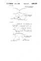
- FIGS. 6A and 6Care sectional views showing the epitaxial growth processes of producing a HEMT structure in a still different embodiment of this invention.
- FIGS. 3A to 3DIts epitaxial growth processes are shown in FIGS. 3A to 3D.
- TMA, TMG, arsinewere used, as the source gases of Al, Ga and As, respectively, in which dimethyl zinc (DMZ) and hydrogen sellenide were used, p- and n-type dopant gases, and H 2 was used as carrier gas.
- DMZdimethyl zinc
- H 2hydrogen sellenide
- As the light source for irradiating the substratea KrF excimer laser (wavelength 249 nm) was used.
- an n-type Al 0 .6 Ga0.4As clad layer 206was grown in 1.5 ⁇ m (FIG. 3A).
- a non-doped Al x Ga 1 As light confinement layerwas grown in a thickness of 0.2 ⁇ m while gradually decreasing the average power of laser light 901 from 3 W/cm 2 to 0 W/cm 2 .
- quantum well laser of GRIN-SCH structure above p- and n-type electrodeswere formed by an expitaxial growth process on the p-type GaAs cup layer 209 and an n-type GaAs substrate 205, respectively.
- the laser characteristicsshows that with a minimum threshold current of 2.5 mA and an output laser power of 20 mW/facet, a quantum well effect with slight fluctuations in growth lots, and satisfactory reproducibility can be effected.
- the quantum well laser of this inventionis a GRIN-SCH laser which has an active layer with a quantum well structure composed of thin films with various compositions, or a light confinement layer between the active layer and clad layer with a gradually varied composition.
- the quantum well structure and the light confinement layerare formed by irradiating the substrate with intermittent laser light and laser light whose intensity is changed continuously, respectively, during the vapor phase epitaxial growth. Therefore it is free from the problems caused by the changeover of the source gases and changes in the flow rate of the source gases, and designed composition changes can be realized at satisfactory reproducibility, so that the reproducibility and reliability of the characteristics of the quantum well laser fabricated can be enhanced, which may bring about excellent value of use and practical effects.
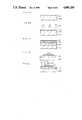
- the appliction of this invention in the epitaxial growth process of an AlGaAs photo transistor structure with a graded bad gap energyis explained below.
- the photo-assisted MOVPE apparatus shown in FIG. 1was used, and trimethyl aluminum [TMA; Al(CH 3 ) 3 ], trimethyl gallium [TMG; Ga(CH 3 ) 3 ], arsine (AsH 3 ) were used, as the source materials of Al, Ga, As, respectively, hydrogen sellinide (H 2 Se) and dimethyl zinc [DMZn; Zn(CH 3 ) 2 ] were used, a n-type and p-type impurity materials, and hydrogen (H 2 ) was used as the carrier gas.
- a KrF excimer laser(wavelength: 249 nm) was used as the light source for irradiation.
- the flow rate of the source materials in each layer growthwere as shown in the table below.
- the average power of the laser light 901was changed by gradually increasing the repetition rate in a range of 9 to 70 Hz, because of the pulse operation of an excimer laser, and the average power of laser light was changed to a maximum of 1.4 W/cm 2 .
- an n-type Al 0 .45 Ga 0 .55 As emitter layer 216was grown in a thickness of 1.4 ⁇ m by irradiating the substrate with a laser light having an average power of 1.4 W/cm 2 , and then stopping laser light irradiation, an n + -type GaAs contact layer 217 was grown in 0.05 ⁇ m in a thickness of succession (FIG. 4C).
- the temperature of the semi-insulating GaAs substrate 220 mounted on a carbon-made susceptor 3 in an epitaxial growth reactor 1was raised to a growth temperature of 750° C. by rf induction.
- AsH 3was supplied at a flow rate of 20 cc/min.
- a an HEMT structurewas formed by growing in the sequence of FIG. 6A, 6B, 6C. In this case, the growth conditions were as shown in the table below.
- the total flow ratewas 5 liter/min, and the reactor pressure during growth was 100 Torr.
- the entire surface of the substratewas irradiated with an ArF excimer laser 902 with an average power of 1.5 W/cm 2 , in the direction perpendicular to the substrate surface, simultaneously with the start of the supply of an n-type impurity material Si(CH 3 ) 4 .
- the method of fabrication of a field effect transistor having a heterojunction structure according to this inventionis to irradiate the substrate surface with a laser light simultaneously with the start of supply of the n-type impurity material having a large photodecomposition efficiency, at the time of the epitaxial growth of the selectively doped semiconductor layer. That is, decomposition of the n-type impurity material is controlled by light irradiation.
- the photo-assisted MOVPE methodmay also be realized in the photo-assisted molecular beam epitaxy (MBE) method, the photo-assisted metal organic molecular beam epitaxy (MOMBE) method, or the photo-assisted vapor phase epitaxy (VPE) method.
- MBEphoto-assisted molecular beam epitaxy
- MOMBEphoto-assisted metal organic molecular beam epitaxy
- VPEphoto-assisted vapor phase epitaxy
- KrF and ArF excimer laser lightswere used, but this invention may be also realized by using other excimer laser lights than KrF and ArF, such as XeF, or an Ar laser light, a CO 2 laser, an He-Cd laser, a YAG laser, etc.
Landscapes
- Engineering & Computer Science (AREA)
- Physics & Mathematics (AREA)
- Condensed Matter Physics & Semiconductors (AREA)
- General Physics & Mathematics (AREA)
- Manufacturing & Machinery (AREA)
- Computer Hardware Design (AREA)
- Microelectronics & Electronic Packaging (AREA)
- Power Engineering (AREA)
- Chemical & Material Sciences (AREA)
- Materials Engineering (AREA)
Abstract
Description
______________________________________ Unit: cc/min GaAs Al.sub.x Ga.sub.1-x As n.sup.+ .GaAs (collector x ≦ 0.2 x = 0.45 (contact Material layer) (base layer) (emitter layer) layer) ______________________________________ TMA -- 0.02 0.1 -- TMG 0.4 0.38 0.3 0.4 AsH.sub.3 20 20 20 20 H.sub.2 Se -- -- -- 0.02 DMZn -- 0.016 -- -- ______________________________________
______________________________________ Ga(CH.sub.3).sub.3 Al(CH.sub.3).sub.3 AsH.sub.3 Si(CH.sub.3).sub.4 (sccm) (sccm) (sccm) (sccm) ______________________________________ (1) Non-doped GaAs 0.4 -- 20 -- layer (2) Non-doped 20 -- AlGaAs layer (3) n-type 20 AlGaAs layer ______________________________________
Claims (4)
Applications Claiming Priority (8)
| Application Number | Priority Date | Filing Date | Title |
|---|---|---|---|
| JP62-33804 | 1987-02-17 | ||
| JP62033804AJPS63200585A (en) | 1987-02-17 | 1987-02-17 | Manufacturing method of quantum well laser |
| JP62-35041 | 1987-02-18 | ||
| JP62035041AJPS63202975A (en) | 1987-02-18 | 1987-02-18 | Manufacturing method of phototransistor |
| JP62-61547 | 1987-03-17 | ||
| JP62061547AJPS63227065A (en) | 1987-03-17 | 1987-03-17 | Manufacturing method of photodetector |
| JP62-154663 | 1987-06-22 | ||
| JP62154663AJPS63318784A (en) | 1987-06-22 | 1987-06-22 | Method for manufacturing field effect transistors |
Publications (1)
| Publication Number | Publication Date |
|---|---|
| US4885260Atrue US4885260A (en) | 1989-12-05 |
Family
ID=27459839
Family Applications (1)
| Application Number | Title | Priority Date | Filing Date |
|---|---|---|---|
| US07/156,525Expired - LifetimeUS4885260A (en) | 1987-02-17 | 1988-02-16 | Method of laser enhanced vapor phase growth for compound semiconductor |
Country Status (1)
| Country | Link |
|---|---|
| US (1) | US4885260A (en) |
Cited By (16)
| Publication number | Priority date | Publication date | Assignee | Title |
|---|---|---|---|---|
| US4948752A (en)* | 1988-08-10 | 1990-08-14 | Itt Corporation | Method of making sagfets on buffer layers |
| US5061643A (en)* | 1989-03-30 | 1991-10-29 | Mitsubishi Denki Kabushiki Kaisha | Method of doping a growing crystalline semiconductor film |
| US5186750A (en)* | 1988-08-15 | 1993-02-16 | Nippon Telegraph And Telephone Corporation | Method and apparatus for forming semiconductor thin films |
| US5238867A (en)* | 1991-07-09 | 1993-08-24 | Posco Educational Foundation | Method for preparing an optical switching device having multiple quantum wells |
| US5252512A (en)* | 1989-11-03 | 1993-10-12 | United Technologies Corporation | TEOV doping of gallium arsenide |
| USH1264H (en) | 1988-04-04 | 1993-12-07 | Xerox Corporation | Method of in situ stoiciometric and geometrical photo induced modifications to compound thin films during epitaxial growth and applications thereof |
| US5270247A (en)* | 1991-07-12 | 1993-12-14 | Fujitsu Limited | Atomic layer epitaxy of compound semiconductor |
| US5273932A (en)* | 1988-08-15 | 1993-12-28 | Nippon Telegraph & Telephone Corp. | Method for forming semiconductor thin films where an argon laser is used to suppress crystal growth |
| US5415128A (en)* | 1991-04-12 | 1995-05-16 | Texas Instruments Incorporated | Rotation induced superlattice |
| US5674766A (en)* | 1994-12-30 | 1997-10-07 | Siliconix Incorporated | Method of making a trench MOSFET with multi-resistivity drain to provide low on-resistance by varying dopant concentration in epitaxial layer |
| US5938839A (en)* | 1991-10-04 | 1999-08-17 | Semiconductor Energy Laboratory Co., Ltd. | Method for forming a semiconductor device |
| US6077718A (en)* | 1985-07-23 | 2000-06-20 | Canon Kabushiki Kaisha | Method for forming deposited film |
| US20030153167A1 (en)* | 1992-11-06 | 2003-08-14 | Semiconductor Energy Laboratory Co., Ltd. | Laser processing apparatus and laser processing process |
| US20070137555A1 (en)* | 2005-10-21 | 2007-06-21 | Haeyeon Yang | Self-assembled nanostructures |
| US20070228394A1 (en)* | 2006-03-31 | 2007-10-04 | Fujifilm Corporation | Semiconductor layer, process for forming the same, and semiconductor light emitting device |
| US20120058627A1 (en)* | 2009-05-01 | 2012-03-08 | V Technology Co., Ltd. | Compound semiconductor deposition method and apparatus |
Citations (8)
| Publication number | Priority date | Publication date | Assignee | Title |
|---|---|---|---|---|
| US4081313A (en)* | 1975-01-24 | 1978-03-28 | Applied Materials, Inc. | Process for preparing semiconductor wafers with substantially no crystallographic slip |
| US4533410A (en)* | 1982-10-19 | 1985-08-06 | Matsushita Electric Industrial Co., Ltd. | Process of vapor phase epitaxy of compound semiconductors |
| US4588451A (en)* | 1984-04-27 | 1986-05-13 | Advanced Energy Fund Limited Partnership | Metal organic chemical vapor deposition of 111-v compounds on silicon |
| US4632711A (en)* | 1984-04-09 | 1986-12-30 | Sumitomo Chemical Company, Limited | Vapor phase epitaxial growth method of zinc selenide and zinc selenide-sulphide by organometallic chemical vapor deposition |
| US4664743A (en)* | 1984-08-21 | 1987-05-12 | British Telecommunications Plc | Growth of semi-conductors and apparatus for use therein |
| US4716130A (en)* | 1984-04-26 | 1987-12-29 | American Telephone And Telegraph Company, At&T Bell Laboratories | MOCVD of semi-insulating indium phosphide based compositions |
| US4729968A (en)* | 1985-09-16 | 1988-03-08 | American Telephone And Telegraph Company, At&T Bell Laboratories | Hydride deposition of phosporus-containing semiconductor materials avoiding hillock formation |
| US4767494A (en)* | 1986-07-04 | 1988-08-30 | Nippon Telegraph & Telephone Corporation | Preparation process of compound semiconductor |
- 1988
- 1988-02-16USUS07/156,525patent/US4885260A/ennot_activeExpired - Lifetime
Patent Citations (8)
| Publication number | Priority date | Publication date | Assignee | Title |
|---|---|---|---|---|
| US4081313A (en)* | 1975-01-24 | 1978-03-28 | Applied Materials, Inc. | Process for preparing semiconductor wafers with substantially no crystallographic slip |
| US4533410A (en)* | 1982-10-19 | 1985-08-06 | Matsushita Electric Industrial Co., Ltd. | Process of vapor phase epitaxy of compound semiconductors |
| US4632711A (en)* | 1984-04-09 | 1986-12-30 | Sumitomo Chemical Company, Limited | Vapor phase epitaxial growth method of zinc selenide and zinc selenide-sulphide by organometallic chemical vapor deposition |
| US4716130A (en)* | 1984-04-26 | 1987-12-29 | American Telephone And Telegraph Company, At&T Bell Laboratories | MOCVD of semi-insulating indium phosphide based compositions |
| US4588451A (en)* | 1984-04-27 | 1986-05-13 | Advanced Energy Fund Limited Partnership | Metal organic chemical vapor deposition of 111-v compounds on silicon |
| US4664743A (en)* | 1984-08-21 | 1987-05-12 | British Telecommunications Plc | Growth of semi-conductors and apparatus for use therein |
| US4729968A (en)* | 1985-09-16 | 1988-03-08 | American Telephone And Telegraph Company, At&T Bell Laboratories | Hydride deposition of phosporus-containing semiconductor materials avoiding hillock formation |
| US4767494A (en)* | 1986-07-04 | 1988-08-30 | Nippon Telegraph & Telephone Corporation | Preparation process of compound semiconductor |
Non-Patent Citations (10)
| Title |
|---|
| Balk et al., "Ultraviolet Induced Metal-Organic Chemical Vapor Deposition Growth of GaAs," J. Voc. Sci. Technol., A4(3) May/Jun. 1986, pp. 711-715. |
| Balk et al., Ultraviolet Induced Metal Organic Chemical Vapor Deposition Growth of GaAs, J. Voc. Sci. Technol., A4(3) May/Jun. 1986, pp. 711 715.* |
| Bedair et al., Appl. Phys. Lett., 48(2), 13 Jan. 1986, pp. 174 176.* |
| Bedair et al., Appl. Phys. Lett., 48(2), 13 Jan. 1986, pp. 174-176. |
| Doi et al., "Stepwise . . . by Switched Laser Metalorganic Vapor Phase Epitaxy", Appl. Phys. Lett., 49(13), 29 Sep. 1986, pp. 785-787. |
| Doi et al., Stepwise . . . by Switched Laser Metalorganic Vapor Phase Epitaxy , Appl. Phys. Lett., 49(13), 29 Sep. 1986, pp. 785 787.* |
| Nishizawa et al., "Molecular Layer Epitaxy", J. Electrochem. Soc., 132, May 1985, pp. 1197-1200. |
| Nishizawa et al., "Photostimulated Molecular Layer Epitaxy", J. Vac. Sci. Technol., A4(3), May/Jun. 1986, pp. 706-710. |
| Nishizawa et al., Molecular Layer Epitaxy , J. Electrochem. Soc., 132, May 1985, pp. 1197 1200.* |
| Nishizawa et al., Photostimulated Molecular Layer Epitaxy , J. Vac. Sci. Technol., A4(3), May/Jun. 1986, pp. 706 710.* |
Cited By (31)
| Publication number | Priority date | Publication date | Assignee | Title |
|---|---|---|---|---|
| US6077718A (en)* | 1985-07-23 | 2000-06-20 | Canon Kabushiki Kaisha | Method for forming deposited film |
| USH1264H (en) | 1988-04-04 | 1993-12-07 | Xerox Corporation | Method of in situ stoiciometric and geometrical photo induced modifications to compound thin films during epitaxial growth and applications thereof |
| US4948752A (en)* | 1988-08-10 | 1990-08-14 | Itt Corporation | Method of making sagfets on buffer layers |
| US5186750A (en)* | 1988-08-15 | 1993-02-16 | Nippon Telegraph And Telephone Corporation | Method and apparatus for forming semiconductor thin films |
| US5273932A (en)* | 1988-08-15 | 1993-12-28 | Nippon Telegraph & Telephone Corp. | Method for forming semiconductor thin films where an argon laser is used to suppress crystal growth |
| US5061643A (en)* | 1989-03-30 | 1991-10-29 | Mitsubishi Denki Kabushiki Kaisha | Method of doping a growing crystalline semiconductor film |
| US5252512A (en)* | 1989-11-03 | 1993-10-12 | United Technologies Corporation | TEOV doping of gallium arsenide |
| US5415128A (en)* | 1991-04-12 | 1995-05-16 | Texas Instruments Incorporated | Rotation induced superlattice |
| US5238867A (en)* | 1991-07-09 | 1993-08-24 | Posco Educational Foundation | Method for preparing an optical switching device having multiple quantum wells |
| US5270247A (en)* | 1991-07-12 | 1993-12-14 | Fujitsu Limited | Atomic layer epitaxy of compound semiconductor |
| US6660575B1 (en) | 1991-10-04 | 2003-12-09 | Semiconductor Energy Laboratory Co., Ltd. | Method for forming a semiconductor device |
| US5938839A (en)* | 1991-10-04 | 1999-08-17 | Semiconductor Energy Laboratory Co., Ltd. | Method for forming a semiconductor device |
| US20040110385A1 (en)* | 1991-10-04 | 2004-06-10 | Semiconductor Energy Laboratory Co., Ltd. | Method for forming a semiconductor device |
| US6919239B2 (en) | 1991-10-04 | 2005-07-19 | Semiconductor Energy Laboratory Co., Ltd. | Method for forming a semiconductor device |
| US20030153167A1 (en)* | 1992-11-06 | 2003-08-14 | Semiconductor Energy Laboratory Co., Ltd. | Laser processing apparatus and laser processing process |
| US7179726B2 (en)* | 1992-11-06 | 2007-02-20 | Semiconductor Energy Laboratory Co., Ltd. | Laser processing apparatus and laser processing process |
| US7799665B2 (en) | 1992-11-06 | 2010-09-21 | Semiconductor Energy Laboratory Co., Ltd. | Laser processing apparatus and laser processing process |
| US20070141859A1 (en)* | 1992-11-06 | 2007-06-21 | Semiconductor Energy Laboratory Co., Ltd. | Laser processing apparatus and laser processing process |
| US5895952A (en)* | 1994-12-30 | 1999-04-20 | Siliconix Incorporated | Trench MOSFET with multi-resistivity drain to provide low on-resistance |
| US5674766A (en)* | 1994-12-30 | 1997-10-07 | Siliconix Incorporated | Method of making a trench MOSFET with multi-resistivity drain to provide low on-resistance by varying dopant concentration in epitaxial layer |
| US7655544B2 (en)* | 2005-10-21 | 2010-02-02 | Utah State University | Self-assembled nanostructures |
| US20070137555A1 (en)* | 2005-10-21 | 2007-06-21 | Haeyeon Yang | Self-assembled nanostructures |
| US20070228394A1 (en)* | 2006-03-31 | 2007-10-04 | Fujifilm Corporation | Semiconductor layer, process for forming the same, and semiconductor light emitting device |
| US7727791B2 (en)* | 2006-03-31 | 2010-06-01 | Fujifilm Corporation | Semiconductor layer, process for forming the same, and semiconductor light emitting device |
| US20120058627A1 (en)* | 2009-05-01 | 2012-03-08 | V Technology Co., Ltd. | Compound semiconductor deposition method and apparatus |
| CN102414795A (en)* | 2009-05-01 | 2012-04-11 | 国立大学法人东京大学 | Method of deposition of chemical compound semiconductor and device |
| KR20120065266A (en)* | 2009-05-01 | 2012-06-20 | 고쿠리츠다이가쿠호우진 도쿄다이가쿠 | Method and apparatus for depositing compound semiconductors |
| EP2426702A4 (en)* | 2009-05-01 | 2014-03-26 | Univ Tokyo | CHEMICAL COMPOUND SEMICONDUCTOR DEPOSITION METHOD AND DEVICE THEREOF |
| US8912079B2 (en)* | 2009-05-01 | 2014-12-16 | The University Of Tokyo | Compound semiconductor deposition method and apparatus |
| CN102414795B (en)* | 2009-05-01 | 2015-06-24 | 国立大学法人东京大学 | Method of deposition of chemical compound semiconductor and device |
| KR101708867B1 (en) | 2009-05-01 | 2017-02-21 | 고쿠리츠다이가쿠호우진 도쿄다이가쿠 | Method of deposition of chemical compound semiconductor and device |
Similar Documents
| Publication | Publication Date | Title |
|---|---|---|
| US4885260A (en) | Method of laser enhanced vapor phase growth for compound semiconductor | |
| JP2587623B2 (en) | Epitaxial crystal growth method for compound semiconductor | |
| EP0877455B1 (en) | Semiconductor light emitting device and method for producing the same | |
| US5945690A (en) | Compound semiconductor device | |
| US5904549A (en) | Methods for growing semiconductors and devices thereof from the alloy semiconductor GaInNAs | |
| JP3048273B2 (en) | Method for constructing quantum wire semiconductor lasers via enhancement of photo-induced deposition during in situ epitaxial growth | |
| US5060028A (en) | High band-gap opto-electronic device | |
| US5204284A (en) | Method of making a high band-gap opto-electronic device | |
| JP3368452B2 (en) | Compound semiconductor device and method of manufacturing the same | |
| DenBaars et al. | Atomic layer epitaxy of compound semiconductors with metalorganic precursors | |
| US5375133A (en) | Surface emitting semiconductor laser and method of manufacture | |
| CA2041942C (en) | Quantum wire fabricated via photo induced evaporation enhancement during in situ epitaxial growth | |
| JP2871712B2 (en) | Light assisted MOCVD method | |
| JP4427924B2 (en) | Method for manufacturing light emitting device | |
| JP3665911B2 (en) | Semiconductor optical device manufacturing method and semiconductor optical device | |
| EP0525297A2 (en) | Method of growing doped crystal | |
| JP3109149B2 (en) | Compound semiconductor crystal growth method | |
| JP2549835B2 (en) | Method for manufacturing compound semiconductor thin film | |
| US7046708B2 (en) | Semiconductor laser device including cladding layer having stripe portion different in conductivity type from adjacent portions | |
| FURUYA et al. | GaInAsP/InP organometallic vapor phase epitaxy for research and fabrication of devices | |
| JPH01214083A (en) | Semiconductor laser device, double hetero wafer and manufacturing method thereof | |
| JPH0917737A (en) | Vapor growth method for semiconductor laminated structure | |
| JPH0590160A (en) | Crystal growth method | |
| JPH08340145A (en) | Compound semiconductor light-emitting element and manufacture thereof | |
| JPS63200585A (en) | Manufacturing method of quantum well laser |
Legal Events
| Date | Code | Title | Description |
|---|---|---|---|
| AS | Assignment | Owner name:MATSUSHITA ELECTRIC INDUSTRIAL CO., LTD., 1006 OAZ Free format text:ASSIGNMENT OF ASSIGNORS INTEREST.;ASSIGNORS:BAN, YUZABURO;MANNO, MASAYA;KUBO, MINORU;AND OTHERS;REEL/FRAME:004830/0448 Effective date:19880208 Owner name:MATSUSHITA ELECTRIC INDUSTRIAL CO., LTD.,JAPAN Free format text:ASSIGNMENT OF ASSIGNORS INTEREST;ASSIGNORS:BAN, YUZABURO;MANNO, MASAYA;KUBO, MINORU;AND OTHERS;REEL/FRAME:004830/0448 Effective date:19880208 | |
| STCF | Information on status: patent grant | Free format text:PATENTED CASE | |
| FEPP | Fee payment procedure | Free format text:PAYOR NUMBER ASSIGNED (ORIGINAL EVENT CODE: ASPN); ENTITY STATUS OF PATENT OWNER: LARGE ENTITY | |
| FEPP | Fee payment procedure | Free format text:PAYER NUMBER DE-ASSIGNED (ORIGINAL EVENT CODE: RMPN); ENTITY STATUS OF PATENT OWNER: LARGE ENTITY Free format text:PAYOR NUMBER ASSIGNED (ORIGINAL EVENT CODE: ASPN); ENTITY STATUS OF PATENT OWNER: LARGE ENTITY | |
| FPAY | Fee payment | Year of fee payment:4 | |
| FPAY | Fee payment | Year of fee payment:8 | |
| FPAY | Fee payment | Year of fee payment:12 |