US4884122A - Method and configuration for testing electronic circuits and integrated circuit chips using a removable overlay layer - Google Patents
Method and configuration for testing electronic circuits and integrated circuit chips using a removable overlay layerDownload PDFInfo
- Publication number
- US4884122A US4884122AUS07/230,654US23065488AUS4884122AUS 4884122 AUS4884122 AUS 4884122AUS 23065488 AUS23065488 AUS 23065488AUS 4884122 AUS4884122 AUS 4884122A
- Authority
- US
- United States
- Prior art keywords
- chips
- package
- chip
- test
- integrated circuit
- Prior art date
- Legal status (The legal status is an assumption and is not a legal conclusion. Google has not performed a legal analysis and makes no representation as to the accuracy of the status listed.)
- Expired - Lifetime
Links
- 238000012360testing methodMethods0.000titleclaimsabstractdescription114
- 238000000034methodMethods0.000titleclaimsabstractdescription36
- 238000001465metallisationMethods0.000claimsabstractdescription24
- 239000000758substrateSubstances0.000claimsdescription21
- 239000013598vectorSubstances0.000claimsdescription11
- 229920006254polymer filmPolymers0.000claimsdescription9
- 230000008569processEffects0.000claimsdescription6
- 230000006870functionEffects0.000claimsdescription2
- 239000000523sampleSubstances0.000abstractdescription16
- 230000010354integrationEffects0.000abstractdescription4
- 238000004519manufacturing processMethods0.000abstractdescription4
- WYURNTSHIVDZCO-UHFFFAOYSA-NTetrahydrofuranChemical compoundC1CCOC1WYURNTSHIVDZCO-UHFFFAOYSA-N0.000description13
- RYGMFSIKBFXOCR-UHFFFAOYSA-NCopperChemical compound[Cu]RYGMFSIKBFXOCR-UHFFFAOYSA-N0.000description11
- 239000010949copperSubstances0.000description11
- 229910052802copperInorganic materials0.000description11
- 239000000463materialSubstances0.000description8
- VYZAMTAEIAYCRO-UHFFFAOYSA-NChromiumChemical compound[Cr]VYZAMTAEIAYCRO-UHFFFAOYSA-N0.000description6
- QAOWNCQODCNURD-UHFFFAOYSA-NSulfuric acidChemical compoundOS(O)(=O)=OQAOWNCQODCNURD-UHFFFAOYSA-N0.000description6
- 229920000642polymerPolymers0.000description6
- YLQBMQCUIZJEEH-UHFFFAOYSA-NtetrahydrofuranNatural productsC=1C=COC=1YLQBMQCUIZJEEH-UHFFFAOYSA-N0.000description6
- 230000002950deficientEffects0.000description5
- 238000004806packaging method and processMethods0.000description5
- RTAQQCXQSZGOHL-UHFFFAOYSA-NTitaniumChemical compound[Ti]RTAQQCXQSZGOHL-UHFFFAOYSA-N0.000description4
- QVGXLLKOCUKJST-UHFFFAOYSA-Natomic oxygenChemical compound[O]QVGXLLKOCUKJST-UHFFFAOYSA-N0.000description4
- 229910052760oxygenInorganic materials0.000description4
- 239000001301oxygenSubstances0.000description4
- 229920002120photoresistant polymerPolymers0.000description4
- 239000010936titaniumSubstances0.000description4
- 229910052719titaniumInorganic materials0.000description4
- XLYOFNOQVPJJNP-UHFFFAOYSA-NwaterSubstancesOXLYOFNOQVPJJNP-UHFFFAOYSA-N0.000description4
- GRYLNZFGIOXLOG-UHFFFAOYSA-NNitric acidChemical compoundO[N+]([O-])=OGRYLNZFGIOXLOG-UHFFFAOYSA-N0.000description3
- 238000013459approachMethods0.000description3
- 230000005540biological transmissionEffects0.000description3
- 230000007774longtermEffects0.000description3
- 229910017604nitric acidInorganic materials0.000description3
- 238000004544sputter depositionMethods0.000description3
- RILZRCJGXSFXNE-UHFFFAOYSA-N2-[4-(trifluoromethoxy)phenyl]ethanolChemical compoundOCCC1=CC=C(OC(F)(F)F)C=C1RILZRCJGXSFXNE-UHFFFAOYSA-N0.000description2
- VVQNEPGJFQJSBK-UHFFFAOYSA-NMethyl methacrylateChemical compoundCOC(=O)C(C)=CVVQNEPGJFQJSBK-UHFFFAOYSA-N0.000description2
- 230000007812deficiencyEffects0.000description2
- 238000010586diagramMethods0.000description2
- 238000001035dryingMethods0.000description2
- 238000005516engineering processMethods0.000description2
- 230000007613environmental effectEffects0.000description2
- 230000003301hydrolyzing effectEffects0.000description2
- 238000007654immersionMethods0.000description2
- 239000000203mixtureSubstances0.000description2
- 238000012986modificationMethods0.000description2
- 230000004048modificationEffects0.000description2
- 238000000638solvent extractionMethods0.000description2
- 238000005507sprayingMethods0.000description2
- QTBSBXVTEAMEQO-UHFFFAOYSA-MAcetateChemical compoundCC([O-])=OQTBSBXVTEAMEQO-UHFFFAOYSA-M0.000description1
- 239000004593EpoxySubstances0.000description1
- 229910003944H3 PO4Inorganic materials0.000description1
- 239000002253acidSubstances0.000description1
- 239000000853adhesiveSubstances0.000description1
- 230000001070adhesive effectEffects0.000description1
- 238000000637aluminium metallisationMethods0.000description1
- 230000004888barrier functionEffects0.000description1
- 230000015556catabolic processEffects0.000description1
- VZDYWEUILIUIDF-UHFFFAOYSA-Jcerium(4+);disulfateChemical compound[Ce+4].[O-]S([O-])(=O)=O.[O-]S([O-])(=O)=OVZDYWEUILIUIDF-UHFFFAOYSA-J0.000description1
- 229910000355cerium(IV) sulfateInorganic materials0.000description1
- 239000011248coating agentSubstances0.000description1
- 238000000576coating methodMethods0.000description1
- 239000004020conductorSubstances0.000description1
- 238000006731degradation reactionMethods0.000description1
- 238000011161developmentMethods0.000description1
- 238000005530etchingMethods0.000description1
- 230000005496eutecticsEffects0.000description1
- 238000007689inspectionMethods0.000description1
- 238000003475laminationMethods0.000description1
- 230000006386memory functionEffects0.000description1
- 230000008520organizationEffects0.000description1
- 238000005192partitionMethods0.000description1
- 238000000059patterningMethods0.000description1
- 238000001020plasma etchingMethods0.000description1
- 229920001721polyimidePolymers0.000description1
- 238000012545processingMethods0.000description1
- CBXWGGFGZDVPNV-UHFFFAOYSA-Nso4-so4Chemical compoundOS(O)(=O)=O.OS(O)(=O)=OCBXWGGFGZDVPNV-UHFFFAOYSA-N0.000description1
- 239000002904solventSubstances0.000description1
- 238000009987spinningMethods0.000description1
- 238000003860storageMethods0.000description1
- 229920001169thermoplasticPolymers0.000description1
- 239000004416thermosoftening plasticSubstances0.000description1
Images


Classifications
- H—ELECTRICITY
- H01—ELECTRIC ELEMENTS
- H01L—SEMICONDUCTOR DEVICES NOT COVERED BY CLASS H10
- H01L23/00—Details of semiconductor or other solid state devices
- H01L23/52—Arrangements for conducting electric current within the device in operation from one component to another, i.e. interconnections, e.g. wires, lead frames
- H01L23/538—Arrangements for conducting electric current within the device in operation from one component to another, i.e. interconnections, e.g. wires, lead frames the interconnection structure between a plurality of semiconductor chips being formed on, or in, insulating substrates
- H01L23/5389—Arrangements for conducting electric current within the device in operation from one component to another, i.e. interconnections, e.g. wires, lead frames the interconnection structure between a plurality of semiconductor chips being formed on, or in, insulating substrates the chips being integrally enclosed by the interconnect and support structures
- G—PHYSICS
- G01—MEASURING; TESTING
- G01R—MEASURING ELECTRIC VARIABLES; MEASURING MAGNETIC VARIABLES
- G01R31/00—Arrangements for testing electric properties; Arrangements for locating electric faults; Arrangements for electrical testing characterised by what is being tested not provided for elsewhere
- G01R31/28—Testing of electronic circuits, e.g. by signal tracer
- G01R31/317—Testing of digital circuits
- G01R31/31723—Hardware for routing the test signal within the device under test to the circuits to be tested, e.g. multiplexer for multiple core testing, accessing internal nodes
- H—ELECTRICITY
- H01—ELECTRIC ELEMENTS
- H01L—SEMICONDUCTOR DEVICES NOT COVERED BY CLASS H10
- H01L23/00—Details of semiconductor or other solid state devices
- H01L23/52—Arrangements for conducting electric current within the device in operation from one component to another, i.e. interconnections, e.g. wires, lead frames
- H01L23/538—Arrangements for conducting electric current within the device in operation from one component to another, i.e. interconnections, e.g. wires, lead frames the interconnection structure between a plurality of semiconductor chips being formed on, or in, insulating substrates
- H01L23/5385—Assembly of a plurality of insulating substrates
- H—ELECTRICITY
- H01—ELECTRIC ELEMENTS
- H01L—SEMICONDUCTOR DEVICES NOT COVERED BY CLASS H10
- H01L23/00—Details of semiconductor or other solid state devices
- H01L23/52—Arrangements for conducting electric current within the device in operation from one component to another, i.e. interconnections, e.g. wires, lead frames
- H01L23/538—Arrangements for conducting electric current within the device in operation from one component to another, i.e. interconnections, e.g. wires, lead frames the interconnection structure between a plurality of semiconductor chips being formed on, or in, insulating substrates
- H01L23/5387—Flexible insulating substrates
- H—ELECTRICITY
- H01—ELECTRIC ELEMENTS
- H01L—SEMICONDUCTOR DEVICES NOT COVERED BY CLASS H10
- H01L2224/00—Indexing scheme for arrangements for connecting or disconnecting semiconductor or solid-state bodies and methods related thereto as covered by H01L24/00
- H01L2224/80—Methods for connecting semiconductor or other solid state bodies using means for bonding being attached to, or being formed on, the surface to be connected
- H01L2224/82—Methods for connecting semiconductor or other solid state bodies using means for bonding being attached to, or being formed on, the surface to be connected by forming build-up interconnects at chip-level, e.g. for high density interconnects [HDI]
- H01L2224/82009—Pre-treatment of the connector or the bonding area
- H01L2224/8203—Reshaping, e.g. forming vias
- H01L2224/82035—Reshaping, e.g. forming vias by heating means
- H01L2224/82039—Reshaping, e.g. forming vias by heating means using a laser
- H—ELECTRICITY
- H01—ELECTRIC ELEMENTS
- H01L—SEMICONDUCTOR DEVICES NOT COVERED BY CLASS H10
- H01L2924/00—Indexing scheme for arrangements or methods for connecting or disconnecting semiconductor or solid-state bodies as covered by H01L24/00
- H01L2924/013—Alloys
- H01L2924/0132—Binary Alloys
- H01L2924/01322—Eutectic Alloys, i.e. obtained by a liquid transforming into two solid phases
Definitions
- the present inventionrelates to packaging electronic integrated circuit chips into operable chip systems in a manner to facilitate testability. More particularly, the present invention relates to a method and configuration employing one or more removable overlay layers containing interconnection metallization patterns. Even more particularly, in one embodiment of the present invention, test chips are packaged with the system chips to exercise the system in its final configuration.
- the present inventionis generally directed to a method for interconnecting integrated circuit chips so as to allow them to be tested in their final configuration in terms of speed, operating environment packaging, temperature, voltage and proximity to other chips of the system.
- a removable overlay layeris applied to chips positioned on a substrate.
- the interconnection pattern of the overlay layeris specifically designed to partition the system for easy testing.
- the interconnect density of the overlay structure and its very low capacitive loadingpermit the utilization of extremely high density patterns which can make interconnection to a chip possible, otherwise, chip systems cannot easily be tested.
- Probe stationsare inadequate for such purposes because too many probes would be required or because the chip pads are too small to accommodate a probe or because the capacitive loading of the probe station is too high to allow the chip to operate at maximum speed.
- test chipsmay also be employed herein These test chips are placed on the substrate along with the operating chip or chip system for the purpose of testing circuits at speeds and under operating conditions which cannot be duplicated at the wafer probe level.
- the overlay layer employed hereinis removable and there is no resulting degradation to the underlying chip.
- the overlay layercan be removed and reapplied several times if necessary with different wiring configurations and with removal and replacement of defective chips until the final operating configuration is established.
- Alternate overlay configurationsare possible. In one configuration, inferior, but easily processed materials are used to provide a test overlay layer thereby simplifying the process and exposing the chips to less stringent processing conditions. In a second configuration, a test overlay layer is applied over an already in place overlay layer for the purpose of simplifying partitioning and multiprobe testing of a complex system.
- the method and configuration of the present inventionis unique in that chips can be arranged in their final operating positions, and connected for the purpose of testing. Then all connections are removed and are reconnected in an operating configuration.
- Other interconnect systemsincluding hybrid circuits, printed circuits and hard-wiring are not amenable to easy removal of all interconnects and reapplication of the interconnections in a different form.
- the problem to be solvedis a multi-faceted one.
- the generic problemis to test a system at the lowest feasible functional level to identify defective parts so that a completely functioning system with a high degree of assured reliability can be produced.
- a first set of problemsresults from the deficiency of probing chips at the wafer level. Wafer probers are limited in speed of the chips that they can test due to the relatively long runs and high capacitive loading associated with the probes. Wafer probes are also limited in the total number of chip pads which can be probed at one time. Wafer probes are also limited by the minimum size of the pad which can be probed. This limitation is exacerbated by large numbers of pads. Additionally, increased pin count is also becoming more prevalent with the advent of very large scale integration since more complexity can now be put on a given chip.
- the typical burn-ininvolves operating the system typically for a period of approximately 100 hours at high temperature conditions. Experience has shown that if a chip is apt to fail, it generally fails under these conditions within the 100 hour time period.
- the conventional approach to testing chipsis to first test the chip at the probe station, recognizing deficiencies in the number of probes and in speed. The chips which pass these tests are packaged. In high reliability systems, the packaged chips are burned-in under power. After burn-in, the package chips are tested again to determine proper functionality. The packaged chips are then interconnected on a printed circuit board to form the final system. Because of size and speed constraints, it is desirable to incorporate several chips in the same package.
- the high density interconnect system disclosed hereinuses an overlay layer to provide a method for directly connecting a large number of chips within the same package.
- the invention disclosed hereinprovides a method for the complete test and burn-in of the chip as well as a practical method for partitioning the system into manageable blocks which are easily tested.
- a removable overlay layercan be used to provide a multiplicity of connections throughout the rest of the system for the purpose of system testing and debugging during and after burn-in. This approach provides the rough equivalence of a " bed of nails" test fixture which is typically used for printed circuit boards but on a pitch of 1 mil rather than a pitch of 50 mils.
- an integrated circuit chip packagecomprises a substrate together with a plurality of integrated circuit chips affixed to the substrate.
- the integrated circuit chipshave interconnect pads thereon for connections to other chips or to different parts of the same chip.
- a polymer film overlayis disposed over the chips and the substrate.
- the filmpossesses apertures aligned with at least some of the interconnect pads.
- the polymer filmalso contains a metallization pattern disposed on the film and operating to connect select interconnect pads.
- the packagealso includes at least one test chip disposed on the substrate and being operable to test at least one other of the chips on the substrate.
- a method for producing integrated circuit chip packagesbegins by affixing a plurality of integrated circuit chips to a substrate.
- the integrated circuit chipspossess interconnect pads, as described above.
- At least one test integrated circuit chipis also disposed on the substrate.
- the test chipincludes means thereon for testably driving at least one of the other chips on the substrate.
- a polymer filmis disposed over the test chip and the other chip or chips.
- the polymer filmpossesses a plurality of apertures, at least some of which are aligned with the interconnect pads, together with a layer of metallization for connecting selected pads on the test chip to selected pads on the other integrated circuit chips. It is noted that more than one test chip may be employed and that these test chips may include memory functions.
- a method for producing integrated circuit chip packagesincludes a step of affixing a plurality of integrated circuit chips to a substrate. As above, the chips possess interconnect pads. Then an overlay layer is applied to the chips and to the substrate. The overlay layer includes a metallization pattern for connecting the chips in a first configuration. This configuration is then preferably tested after which the first overlay layer is removed and a second overlay layer is applied so as to connect the chips in a second configuration. In general, the second configuration is the one in which all parts of the system are connected for final use. It is noted that in this embodiment, the utilization of a test chip is not required.
- Another object of the present inventionis to provide a method in which chips can be tested completely with a pad count which exceeds the capability of probe testing with pad sizes which are below the capacity of probe testing.
- Yet another object of the present inventionis to provide for functional testing of multiplely interconnected chips.
- Yet another object of the present inventionis to provide a method of making a removable interconnection to a multiplicity of points in an integrated circuit chip system already connected by an overlay interconnect method, thereby allowing for complete system test with minimal increase in external probe, pins and drivers.
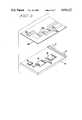
- FIG. 1is an exploded isometric view illustrating a multichip circuit with a test overlay layer
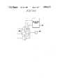
- FIG. 2is an exploded view similar to FIG. 1 but more particularly showing the utilization of a special test chip connected to the other chips in the circuit by means of a different overlay layer;
- FIG. 3is an exploded isometric view illustrating a multichip circuit package with operational overlay layer
- FIG. 4Aillustrates means to probe internal test points with a reduced number of external pins
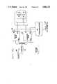
- FIG. 4Bis a schematic diagram illustrating the use of memory means to supply test vectors and to store test results on a packaged substrate assembly
- FIG. 4Cis a schematic diagram similar to FIG. 4B more particularly illustrating the utilization of a microcomputer chip to compute test vectors and to evaluate test results;
- FIG. 5is an exploded isometric view illustrating a multichip circuit assembly which simultaneously employs an operational circuit overlay layer and a test overlay layer.
- a related patent application Serial No. 240,367, filed Aug. 30, 1988, as a continuation of application Ser. No. 912,458 filed Sept. 26, 1986describes a method and apparatus for applying a removable polymer overlay layer:
- a second related patent application Ser. No. now U.S. Pat. No. 4,714,516 issued Dec. 22, 1987, Ser. No. 912,455 filed Sept. 26, 1986descries a preferable method for supplying the overlay layer with a pattern of apertures for connection to the above-described interconnect pads.
- a third related patent application Ser. No. 912,456 filed Sept. 26, 1986 now U.S. Pat. No. 4,783,695, issued Nov. 8, 1988describes a method for providing a preferred form of metallization patterning over a polymer film. All three of these applications are hereby incorporated herein by reference. These applications are assigned to the same assignee as the present invention.
- the first of the aforementioned patent applicationsin particular discloses a method involving few steps and using easy-to-use materials.
- the methods disclosed thereinare generally more suitable for test layers since the test layer is easily processed and easily removed and since long term thermal and hydrolitic stability is not required.
- FIG. 1shows an exploded view of a multichip circuit with overlay layer 20 configured so as to test chips 15 on substrate 10.
- chips 15are affixed to substrate 10, as by bonding in place by conventional means using epoxy bonding, thermoplastic bonding, or eutectic die bonding.
- Polymer overlay layer 20is applied by the following method. Two coats of a solution of methylmethacrylate in THF (tetrahydrofuran) are sprayed over chips 15 with interconnect pads 16. Each coat is dried at a temperature of approximately 150° C. for a period of about 5 minutes. A sheet of acetate film 1 mil in thickness is laminated to the top of the chips and to package pins 11. A vacuum pressure laminator is preferably employed.
- Preferable lamination conditionscomprise a pressure of approximately 30 pounds per square inch at a temperature of about 120° C. for a period of about 3 minutes.
- the substrateis then cooled to 80° C. and removed from the laminator.
- Via holes over the appropriate chip pads and package pinout padsare fabricated using a focused laser according to the method outlined in U.S. Pat. No. 4,714,516 issued Dec. 22, 1987.
- Plasma etchingis accomplished using somewhat less stringent conditions than required for high stability polymers.
- Metallizationis preferably provided by sputtering a 1,000 angstrom thick layer of titanium, followed by a layer of 1 micron thick copper.
- the metallizationis preferably patterned by spraying or spinning a coating of photoresist on the copper surface, drying for about one half hour at approximately 90° C. and exposing the positive resist material with a scanned ultraviolet laser under control of computerized artwork.
- a preferable photoresist materialincludes Dynachem OFPR 800 photoresist. Details of a preferred laser exposure system are disclosed in U.S. Pat. No.
- the desired metallization patternis etched using an acid mix comprising 600 grams of nitric acid, 600 grams of sulfuric acid and 600 grams of H 3 PO 4 in 1.5 liters of water to remove the copper layer, if present.
- a mixturecomprising 1 part fluoroboric acid and 9 parts water is used to remove the titanium layer.
- the circuitis now ready for testing according to the metallization pattern illustrated in FIG. 1.
- the pattern of FIG. 1is used to connect package pins 11 to pads 16 on each chip 15, as required for testing. All testing is conducted by applying signals to inputs through the package pins and observing the resultant outputs at the package pins, at least in the embodiment illustrated in FIG. 1.
- via holes 26are aligned with pads 16 on chips 15. It is also noted that vias 21 are aligned with package pins 11. It is further noted that metallization patterns 22 generally extend from via openings 21 to via openings 26 at least for the sample test configuration shown. This pattern may, however, vary over a wide range of patterns.
- FIG. 2illustrates an alternate embodiment of the present invention in which test chip 14 is used.
- Test chip 14is connected to metallization patterns on overlay layer 20' by means of via openings 24. It is seen in FIG. 2 that overlay layer 20' now makes connections between chip pads 16 and test chip 14. It is noted that more than one test chip may be employed even though the figure illustrates only a single one being used. In the example illustrated in FIG. 2, only two connections 23 are shown as being required between the test chip and the package pins. It can be seen through the use of the test chip that packaging pins can be conserved.
- FIGS. 1 or 2may then be employed to test chips 15. Following the testing, overlay layers 20 or 20' may be removed. Defective chips may be removed or reconfigured or repositioned on the basis of test results obtained. Subsequently, an operational circuit overlay layer 2" may be applied to the chip configuration. As a result, the system illustrated in FIG. 3 may be produced. It is noted that the chief difference between FIG. 1 and FIG. 3 is the particular metallization pattern employed.
- FIGS. 4A, 4B and 4Cshow three alternate implementations of test chips. In all cases, these configurations consist of circuits and technologies well known to those skilled in the art.
- FIG. 4Aillustrates an array of three transmission gates 38 (typically in CMOS technology).
- One of the three transmission gatescan be selected by selection logic 37.
- the data selectorapplies the appropriate signal voltages to transmission gates 38 to turn one of the three gates on and to connect external pad 34 to one of three or more possible internal connection points. It is clear that a number of internal connection points can be multiplexed to one outside pin by this method.
- the very high density interconnect capability afforded by the overlay layerallows this method to act as a multiprobe connection system.
- FIG. 4Billustrates an alternate embodiment of the present invention in which memory means 32, such as a random access memory, is employed as a vector generator to supply test vectors to the inputs of a chip or group of chips 15 under test.
- the output of the chip or group of chipsis stored in second memory means 33 also typically comprising a random access memory.
- Counter 31 driven by clock 30provides sequential addresses to sequence the output of test vectors and the storage of test results.
- This systemcan be run at very high speed, limited only by the speed of the memory means selected
- the test vectorsare supplied at a much more leisurely pace through external input pins 35. Inspection of the results is achieved in a much more leisurely pace by supplying the contents of memory means 33 to external pins 34.
- lines having a hash mark (/)denote multiple signal and/or control paths.
- FIG. 4Cshows a completely internal configuration for high speed testing.
- microprocessor 40computes test vectors and supplies them to vector generation random access memory 32.
- the memoryis sequentially accessed by the associated counter and the output memory supplies the inputs to a chip or a group of chips 15 under test.
- the resultant outputs from the testare stored in second memory means 33.
- microprocessor 40reads the test results and compares them to computed results to determine if errors have occurred.
- the entire systemcan be tested over a long period of time under temperature and variations of other environmental conditions such as electromagnetic interference without any connection, other than power supply, to the outside world.
- Microprocessorscan be used to store test results inconsistent with the expected results, thereby identifying the specific chip or chip group and the failure which occurred, even when the failure occurs on an intermittent basis.
- Microprocessor 40is accessed via external pins 41.
- the test layeris removed according to the following method.
- copper metallizationis dissolved in a solution preferably comprising 600 grams of nitric acid, 600 grams sulfuric acid and 600 grams of H in 1.5 liters of water for a period of about 1 minute. This removes copper, but does not attack either aluminum metallization typically present on the chip pads or titanium which is also preferably (though optionally) present as a barrier layer. Titanium is preferably removed by placement in a solution of fluoroboric acid for a period of about 15 seconds.
- the overlay polymer and adhesivecan be removed in a solution of THF for a period of 2 minutes followed by immersion in another clean solution of THF for 1 minute.
- test layer processas described above can be started immediately after a defective chip has been removed and a new one put in place.
- a plasma etch to remove any residual polymeris also preferred.
- Etch conditionspreferably include an atmosphere comprising 50% oxygen and 50% CF 4 at a total pressure of 0.4 torr for a period of about 21/2 minutes in an IPC 2000 barrel etcher at a power level of approximately 300 watts.
- the final layeris then provided according to the process described in patent application Serial No. 240,367, filed Aug. 30, 1988, as continuation of application Ser. No. 912,458, filed Sept. 26, 1986.
- FIG. 3illustrates an exploded view of tested chips on a substrate with an interconnection pattern for an operational circuit. Note that this pattern is completely different from the test patterns shown in FIGS. 1 or 2.
- the materials used for the final operational configurationpreferably involve materials of long term thermal and hydrolitic stability such as KAPTONTM (supplied by Dupont de Nemours Company, Inc.) polyimide film.
- the metallization usedpreferably comprises slightly thicker material to obviate any problems associated with electromigration or losses due to resistive paths.
- FIG. 5An alternate approach involving the use of an overlay test layer is shown in an exploded view in FIG. 5. This is the same circuit as shown in FIG. 3 except that additional overlay layer 60 has been added to provide connections to the test chip or chips, and to the test pins of the package. Also note that operational circuit overlay layer 50 is similar to overlay layer 20" illustrated in FIG. 3 except for the presence of apertures 24 for connection to test chip 14.
- Test layer 0can be added by spraying a solution of methylmethacrylate in THF and drying at a temperature of approximately 150° C. for a period of 5 minutes. Two such coats are generally required. At this point, via holes re fabricated to the connection points on the layer below by using focused laser energy as described in above-mentioned U.S. Pat. No.
- Etch time in an oxygen plasma to clean out the aperturesis relatively short since the layer is thin and since the material is highly susceptible to etching.
- Etch conditions200 watts for 4 minutes in an atmosphere comprising 30% CF 4 and 70% oxygen at a pressure of 0.4 Torr is sufficient.
- Metallizationis preferably added by sputtering a layer of chrome which is approximately 1,000 angstroms thick, followed by sputtering of sufficient copper for conductivity, typically 1 micron in thickness.
- Metallizationis patterned, as described above, by a photolithographic method using an etchant of nitric acid, sulfuric acid and H in water, as above. This etchant etches the copper but not the chrome.
- Chromeis etched in a ceric sulfate solution operated at 60° C.
- the test layeris easily removed by dissolving the copper in a copper etch solution. This etch attacks the copper, but does not attack the chrome layer. In this way, the underlying chrome layer protects the copper conductor of the underlying layer where it would be exposed at the interconnect points.
- the chromeis removed with a 25 second etch in the sulfate sulfate solution.
- the test layer polymer dielectriccan be removed in a solution of THF, followed by a second immersion in clean THF to remove any residue.
- the underlying KAPTONTM film of the operational interconnect overlayis totally uneffected by the THF solvent.
- the method and configuration of the present inventionfulfills all of the stated objectives.
- a methodis provided for testing integrated circuit chip subsystems to effectively provide wafer scale integration without its concomitant problems.
- multi-chip integrated circuit systemscan be constructed which would otherwise be untestable.
- the systems of the present inventioncan be tested in configurations substantially identical to their operating conditions in terms of capacitive loading, thermal environments and speed.
- the packaging method of the present inventionpermits the utilization of special test chips and thereby significantly reduces investment in special test systems. It is also seen that special testing can be done off line an that testing is accomplished at very high speeds. Accordingly, it is seen that the method and configuration of the present invention significantly advances the art of integrated circuit packaging.
Landscapes
- Engineering & Computer Science (AREA)
- Physics & Mathematics (AREA)
- General Physics & Mathematics (AREA)
- Condensed Matter Physics & Semiconductors (AREA)
- Computer Hardware Design (AREA)
- Microelectronics & Electronic Packaging (AREA)
- Power Engineering (AREA)
- Computer Networks & Wireless Communication (AREA)
- General Engineering & Computer Science (AREA)
- Testing Or Measuring Of Semiconductors Or The Like (AREA)
Abstract
Description
Claims (12)
Priority Applications (2)
| Application Number | Priority Date | Filing Date | Title |
|---|---|---|---|
| US07/230,654US4884122A (en) | 1988-08-05 | 1988-08-05 | Method and configuration for testing electronic circuits and integrated circuit chips using a removable overlay layer |
| US07/414,895US4937203A (en) | 1986-09-26 | 1989-09-29 | Method and configuration for testing electronic circuits and integrated circuit chips using a removable overlay layer |
Applications Claiming Priority (1)
| Application Number | Priority Date | Filing Date | Title |
|---|---|---|---|
| US07/230,654US4884122A (en) | 1988-08-05 | 1988-08-05 | Method and configuration for testing electronic circuits and integrated circuit chips using a removable overlay layer |
Related Parent Applications (1)
| Application Number | Title | Priority Date | Filing Date |
|---|---|---|---|
| US91245486AContinuation | 1986-09-26 | 1986-09-26 |
Related Child Applications (1)
| Application Number | Title | Priority Date | Filing Date |
|---|---|---|---|
| US07/414,895DivisionUS4937203A (en) | 1986-09-26 | 1989-09-29 | Method and configuration for testing electronic circuits and integrated circuit chips using a removable overlay layer |
Publications (1)
| Publication Number | Publication Date |
|---|---|
| US4884122Atrue US4884122A (en) | 1989-11-28 |
Family
ID=22866067
Family Applications (1)
| Application Number | Title | Priority Date | Filing Date |
|---|---|---|---|
| US07/230,654Expired - LifetimeUS4884122A (en) | 1986-09-26 | 1988-08-05 | Method and configuration for testing electronic circuits and integrated circuit chips using a removable overlay layer |
Country Status (1)
| Country | Link |
|---|---|
| US (1) | US4884122A (en) |
Cited By (67)
| Publication number | Priority date | Publication date | Assignee | Title |
|---|---|---|---|---|
| EP0465199A1 (en)* | 1990-07-02 | 1992-01-08 | General Electric Company | Multiple lamination high density interconnect process and structure |
| US5091769A (en)* | 1991-03-27 | 1992-02-25 | Eichelberger Charles W | Configuration for testing and burn-in of integrated circuit chips |
| WO1992005582A1 (en)* | 1990-09-24 | 1992-04-02 | Tessera, Inc. | Semiconductor chip assemblies, methods of making same and components for same |
| US5111278A (en)* | 1991-03-27 | 1992-05-05 | Eichelberger Charles W | Three-dimensional multichip module systems |
| EP0481703A3 (en)* | 1990-10-15 | 1992-08-05 | Aptix Corporation | Interconnect structure for use with programming elements and test devices |
| US5144747A (en)* | 1991-03-27 | 1992-09-08 | Integrated System Assemblies Corporation | Apparatus and method for positioning an integrated circuit chip within a multichip module |
| US5146303A (en)* | 1990-04-05 | 1992-09-08 | General Electric Company | Compact, thermally efficient focal plane array and testing and repair thereof |
| US5148266A (en)* | 1990-09-24 | 1992-09-15 | Ist Associates, Inc. | Semiconductor chip assemblies having interposer and flexible lead |
| US5157255A (en)* | 1990-04-05 | 1992-10-20 | General Electric Company | Compact, thermally efficient focal plane array and testing and repair thereof |
| US5166605A (en)* | 1991-08-02 | 1992-11-24 | General Electric Company | Controlled impedance test fixture for planar electronic device |
| US5200810A (en)* | 1990-04-05 | 1993-04-06 | General Electric Company | High density interconnect structure with top mounted components |
| US5206712A (en)* | 1990-04-05 | 1993-04-27 | General Electric Company | Building block approach to microwave modules |
| US5250843A (en)* | 1991-03-27 | 1993-10-05 | Integrated System Assemblies Corp. | Multichip integrated circuit modules |
| US5257178A (en)* | 1991-12-19 | 1993-10-26 | General Electric Company | Method of optimally operating a computer numerical control milling machine to mill optimal high density interconnect substrates |
| US5258330A (en)* | 1990-09-24 | 1993-11-02 | Tessera, Inc. | Semiconductor chip assemblies with fan-in leads |
| US5324687A (en)* | 1992-10-16 | 1994-06-28 | General Electric Company | Method for thinning of integrated circuit chips for lightweight packaged electronic systems |
| US5336928A (en)* | 1992-09-18 | 1994-08-09 | General Electric Company | Hermetically sealed packaged electronic system |
| US5347145A (en)* | 1990-12-27 | 1994-09-13 | Kabushiki Kaisha Toshiba | Pad arrangement for a semiconductor device |
| US5351001A (en)* | 1990-04-05 | 1994-09-27 | General Electric Company | Microwave component test method and apparatus |
| US5366906A (en)* | 1992-10-16 | 1994-11-22 | Martin Marietta Corporation | Wafer level integration and testing |
| US5373188A (en)* | 1992-11-04 | 1994-12-13 | Mitsubishi Denki Kabushiki Kaisha | Packaged semiconductor device including multiple semiconductor chips and cross-over lead |
| US5386127A (en)* | 1990-04-25 | 1995-01-31 | Kabushiki Kaisha Toshiba | Semiconductor device having groups of pads which receive the same signal |
| US5399505A (en)* | 1993-07-23 | 1995-03-21 | Motorola, Inc. | Method and apparatus for performing wafer level testing of integrated circuit dice |
| US5410179A (en)* | 1990-04-05 | 1995-04-25 | Martin Marietta Corporation | Microwave component having tailored operating characteristics and method of tailoring |
| US5448179A (en)* | 1994-07-12 | 1995-09-05 | The United States Of America As Represented By The Secretary Of The Air Force | Screening of conductors and contacts on microelectronic devices |
| US5452182A (en)* | 1990-04-05 | 1995-09-19 | Martin Marietta Corporation | Flexible high density interconnect structure and flexibly interconnected system |
| US5455459A (en)* | 1992-03-27 | 1995-10-03 | Martin Marietta Corporation | Reconstructable interconnect structure for electronic circuits |
| US5532817A (en)* | 1994-10-03 | 1996-07-02 | The Dow Chemical Company | Method of optical inspection |
| US5594273A (en)* | 1993-07-23 | 1997-01-14 | Motorola Inc. | Apparatus for performing wafer-level testing of integrated circuits where test pads lie within integrated circuit die but overly no active circuitry for improved yield |
| US5631502A (en)* | 1993-03-15 | 1997-05-20 | Kabushiki Kaisha Toshiba | Multi-chip module |
| US5654588A (en)* | 1993-07-23 | 1997-08-05 | Motorola Inc. | Apparatus for performing wafer-level testing of integrated circuits where the wafer uses a segmented conductive top-layer bus structure |
| US5666480A (en)* | 1991-11-05 | 1997-09-09 | Monolithic System Technology, Inc. | Fault-tolerant hierarchical bus system and method of operating same |
| US5679977A (en)* | 1990-09-24 | 1997-10-21 | Tessera, Inc. | Semiconductor chip assemblies, methods of making same and components for same |
| US5701666A (en)* | 1994-08-31 | 1997-12-30 | Motorola, Inc. | Method for manufacturing a stimulus wafer for use in a wafer-to-wafer testing system to test integrated circuits located on a product wafer |
| US5737587A (en)* | 1991-11-05 | 1998-04-07 | Monolithic System Technology, Inc. | Resynchronization circuit for circuit module architecture |
| US5770884A (en)* | 1995-06-30 | 1998-06-23 | International Business Machines Corporation | Very dense integrated circuit package |
| US5814885A (en)* | 1997-04-28 | 1998-09-29 | International Business Machines Corporation | Very dense integrated circuit package |
| US5820014A (en) | 1993-11-16 | 1998-10-13 | Form Factor, Inc. | Solder preforms |
| US5831467A (en)* | 1991-11-05 | 1998-11-03 | Monolithic System Technology, Inc. | Termination circuit with power-down mode for use in circuit module architecture |
| US5841931A (en)* | 1996-11-26 | 1998-11-24 | Massachusetts Institute Of Technology | Methods of forming polycrystalline semiconductor waveguides for optoelectronic integrated circuits, and devices formed thereby |
| US5843799A (en)* | 1991-11-05 | 1998-12-01 | Monolithic System Technology, Inc. | Circuit module redundancy architecture process |
| US5844297A (en)* | 1995-09-26 | 1998-12-01 | Symbios, Inc. | Antifuse device for use on a field programmable interconnect chip |
| US5858815A (en)* | 1996-06-21 | 1999-01-12 | Anam Semiconductor Inc. | Semiconductor package and method for fabricating the same |
| US5897728A (en)* | 1989-02-03 | 1999-04-27 | Lockheed Martin Corporation | Integrated circuit test structure and test process |
| US5936311A (en)* | 1996-12-31 | 1999-08-10 | Intel Corporation | Integrated circuit alignment marks distributed throughout a surface metal line |
| US5937276A (en)* | 1996-12-13 | 1999-08-10 | Tessera, Inc. | Bonding lead structure with enhanced encapsulation |
| US5994152A (en) | 1996-02-21 | 1999-11-30 | Formfactor, Inc. | Fabricating interconnects and tips using sacrificial substrates |
| US5998868A (en)* | 1998-02-04 | 1999-12-07 | International Business Machines Corporation | Very dense chip package |
| US6025638A (en)* | 1998-06-01 | 2000-02-15 | International Business Machines Corporation | Structure for precision multichip assembly |
| US6028986A (en)* | 1995-11-10 | 2000-02-22 | Samsung Electronics Co., Ltd. | Methods of designing and fabricating intergrated circuits which take into account capacitive loading by the intergrated circuit potting material |
| US6066513A (en)* | 1998-10-02 | 2000-05-23 | International Business Machines Corporation | Process for precise multichip integration and product thereof |
| US6087199A (en)* | 1998-02-04 | 2000-07-11 | International Business Machines Corporation | Method for fabricating a very dense chip package |
| US6110806A (en)* | 1999-03-26 | 2000-08-29 | International Business Machines Corporation | Process for precision alignment of chips for mounting on a substrate |
| US6159767A (en)* | 1996-05-20 | 2000-12-12 | Epic Technologies, Inc. | Single chip modules, repairable multichip modules, and methods of fabrication thereof |
| US6239980B1 (en) | 1998-08-31 | 2001-05-29 | General Electric Company | Multimodule interconnect structure and process |
| US20010009032A1 (en)* | 1989-09-20 | 2001-07-19 | Mohsen Amr M. | Structure having multiple levels of programmable integrated circuits for interconnecting electronic components |
| US6274391B1 (en) | 1992-10-26 | 2001-08-14 | Texas Instruments Incorporated | HDI land grid array packaged device having electrical and optical interconnects |
| US6274823B1 (en) | 1993-11-16 | 2001-08-14 | Formfactor, Inc. | Interconnection substrates with resilient contact structures on both sides |
| US6333553B1 (en) | 1999-05-21 | 2001-12-25 | International Business Machines Corporation | Wafer thickness compensation for interchip planarity |
| US6444560B1 (en) | 2000-09-26 | 2002-09-03 | International Business Machines Corporation | Process for making fine pitch connections between devices and structure made by the process |
| US6864165B1 (en) | 2003-09-15 | 2005-03-08 | International Business Machines Corporation | Method of fabricating integrated electronic chip with an interconnect device |
| US20050194961A1 (en)* | 2004-03-04 | 2005-09-08 | Summers Steven M. | On board built in test |
| US7098078B2 (en) | 1990-09-24 | 2006-08-29 | Tessera, Inc. | Microelectronic component and assembly having leads with offset portions |
| US20070283191A1 (en)* | 2003-12-19 | 2007-12-06 | Mcdonald-Maier Klaus D | Integrated Circuit with Debug Support Interface |
| US7485562B2 (en)* | 2002-08-27 | 2009-02-03 | Micron Technology, Inc. | Method of making multichip wafer level packages and computing systems incorporating same |
| US7601039B2 (en) | 1993-11-16 | 2009-10-13 | Formfactor, Inc. | Microelectronic contact structure and method of making same |
| US8033838B2 (en) | 1996-02-21 | 2011-10-11 | Formfactor, Inc. | Microelectronic contact structure |
Citations (8)
| Publication number | Priority date | Publication date | Assignee | Title |
|---|---|---|---|---|
| US3614832A (en)* | 1966-03-09 | 1971-10-26 | Ibm | Decal connectors and methods of forming decal connections to solid state devices |
| US3679941A (en)* | 1969-09-22 | 1972-07-25 | Gen Electric | Composite integrated circuits including semiconductor chips mounted on a common substrate with connections made through a dielectric encapsulator |
| US3746973A (en)* | 1972-05-05 | 1973-07-17 | Ibm | Testing of metallization networks on insulative substrates supporting semiconductor chips |
| US3757175A (en)* | 1971-01-06 | 1973-09-04 | Soo Kim Chang | Tor chips mounted on a single substrate composite integrated circuits with coplnaar connections to semiconduc |
| US3803483A (en)* | 1972-05-05 | 1974-04-09 | Ibm | Semiconductor structure for testing of metallization networks on insulative substrates supporting semiconductor chips |
| US4246595A (en)* | 1977-03-08 | 1981-01-20 | Matsushita Electric Industrial Co., Ltd. | Electronics circuit device and method of making the same |
| US4721995A (en)* | 1984-10-05 | 1988-01-26 | Fujitsu Limited | Integrated circuit semiconductor device formed on a wafer |
| US4783695A (en)* | 1986-09-26 | 1988-11-08 | General Electric Company | Multichip integrated circuit packaging configuration and method |
- 1988
- 1988-08-05USUS07/230,654patent/US4884122A/ennot_activeExpired - Lifetime
Patent Citations (8)
| Publication number | Priority date | Publication date | Assignee | Title |
|---|---|---|---|---|
| US3614832A (en)* | 1966-03-09 | 1971-10-26 | Ibm | Decal connectors and methods of forming decal connections to solid state devices |
| US3679941A (en)* | 1969-09-22 | 1972-07-25 | Gen Electric | Composite integrated circuits including semiconductor chips mounted on a common substrate with connections made through a dielectric encapsulator |
| US3757175A (en)* | 1971-01-06 | 1973-09-04 | Soo Kim Chang | Tor chips mounted on a single substrate composite integrated circuits with coplnaar connections to semiconduc |
| US3746973A (en)* | 1972-05-05 | 1973-07-17 | Ibm | Testing of metallization networks on insulative substrates supporting semiconductor chips |
| US3803483A (en)* | 1972-05-05 | 1974-04-09 | Ibm | Semiconductor structure for testing of metallization networks on insulative substrates supporting semiconductor chips |
| US4246595A (en)* | 1977-03-08 | 1981-01-20 | Matsushita Electric Industrial Co., Ltd. | Electronics circuit device and method of making the same |
| US4721995A (en)* | 1984-10-05 | 1988-01-26 | Fujitsu Limited | Integrated circuit semiconductor device formed on a wafer |
| US4783695A (en)* | 1986-09-26 | 1988-11-08 | General Electric Company | Multichip integrated circuit packaging configuration and method |
Non-Patent Citations (2)
| Title |
|---|
| The STD Process New Development and Applications Clark et al. pp. 131 144, 1974, International Microwave Symposium.* |
| The STD Process-New Development and Applications-Clark et al.-pp. 131-144, 1974, International Microwave Symposium. |
Cited By (103)
| Publication number | Priority date | Publication date | Assignee | Title |
|---|---|---|---|---|
| US5897728A (en)* | 1989-02-03 | 1999-04-27 | Lockheed Martin Corporation | Integrated circuit test structure and test process |
| US20010009032A1 (en)* | 1989-09-20 | 2001-07-19 | Mohsen Amr M. | Structure having multiple levels of programmable integrated circuits for interconnecting electronic components |
| US20020100010A1 (en)* | 1989-09-20 | 2002-07-25 | Aptix Corporation | Field programmable printed circuit board |
| US5410179A (en)* | 1990-04-05 | 1995-04-25 | Martin Marietta Corporation | Microwave component having tailored operating characteristics and method of tailoring |
| US5206712A (en)* | 1990-04-05 | 1993-04-27 | General Electric Company | Building block approach to microwave modules |
| US5452182A (en)* | 1990-04-05 | 1995-09-19 | Martin Marietta Corporation | Flexible high density interconnect structure and flexibly interconnected system |
| US5146303A (en)* | 1990-04-05 | 1992-09-08 | General Electric Company | Compact, thermally efficient focal plane array and testing and repair thereof |
| US5351001A (en)* | 1990-04-05 | 1994-09-27 | General Electric Company | Microwave component test method and apparatus |
| US5157255A (en)* | 1990-04-05 | 1992-10-20 | General Electric Company | Compact, thermally efficient focal plane array and testing and repair thereof |
| US5200810A (en)* | 1990-04-05 | 1993-04-06 | General Electric Company | High density interconnect structure with top mounted components |
| US5386127A (en)* | 1990-04-25 | 1995-01-31 | Kabushiki Kaisha Toshiba | Semiconductor device having groups of pads which receive the same signal |
| US5161093A (en)* | 1990-07-02 | 1992-11-03 | General Electric Company | Multiple lamination high density interconnect process and structure employing a variable crosslinking adhesive |
| EP0465199A1 (en)* | 1990-07-02 | 1992-01-08 | General Electric Company | Multiple lamination high density interconnect process and structure |
| US7098078B2 (en) | 1990-09-24 | 2006-08-29 | Tessera, Inc. | Microelectronic component and assembly having leads with offset portions |
| US5679977A (en)* | 1990-09-24 | 1997-10-21 | Tessera, Inc. | Semiconductor chip assemblies, methods of making same and components for same |
| US6372527B1 (en) | 1990-09-24 | 2002-04-16 | Tessera, Inc. | Methods of making semiconductor chip assemblies |
| US5258330A (en)* | 1990-09-24 | 1993-11-02 | Tessera, Inc. | Semiconductor chip assemblies with fan-in leads |
| US6392306B1 (en) | 1990-09-24 | 2002-05-21 | Tessera, Inc. | Semiconductor chip assembly with anisotropic conductive adhesive connections |
| WO1992005582A1 (en)* | 1990-09-24 | 1992-04-02 | Tessera, Inc. | Semiconductor chip assemblies, methods of making same and components for same |
| US6133627A (en)* | 1990-09-24 | 2000-10-17 | Tessera, Inc. | Semiconductor chip package with center contacts |
| US7198969B1 (en) | 1990-09-24 | 2007-04-03 | Tessera, Inc. | Semiconductor chip assemblies, methods of making same and components for same |
| US5346861A (en)* | 1990-09-24 | 1994-09-13 | Tessera, Inc. | Semiconductor chip assemblies and methods of making same |
| US5682061A (en)* | 1990-09-24 | 1997-10-28 | Tessera, Inc. | Component for connecting a semiconductor chip to a substrate |
| US7291910B2 (en) | 1990-09-24 | 2007-11-06 | Tessera, Inc. | Semiconductor chip assemblies, methods of making same and components for same |
| US6433419B2 (en) | 1990-09-24 | 2002-08-13 | Tessera, Inc. | Face-up semiconductor chip assemblies |
| US5950304A (en)* | 1990-09-24 | 1999-09-14 | Tessera, Inc. | Methods of making semiconductor chip assemblies |
| US6465893B1 (en) | 1990-09-24 | 2002-10-15 | Tessera, Inc. | Stacked chip assembly |
| US7271481B2 (en) | 1990-09-24 | 2007-09-18 | Tessera, Inc. | Microelectronic component and assembly having leads with offset portions |
| US5148266A (en)* | 1990-09-24 | 1992-09-15 | Ist Associates, Inc. | Semiconductor chip assemblies having interposer and flexible lead |
| EP0481703A3 (en)* | 1990-10-15 | 1992-08-05 | Aptix Corporation | Interconnect structure for use with programming elements and test devices |
| US5973340A (en)* | 1990-10-15 | 1999-10-26 | Aptix Corporation | Interconnect substrate with circuits for field-programmability and testing of multichip modules and hybrid circuits |
| US5504354A (en)* | 1990-10-15 | 1996-04-02 | Aptix Corporation | Interconnect substrate with circuits for field-programmability and testing of multichip modules and hybrid circuits |
| US5654564A (en)* | 1990-10-15 | 1997-08-05 | Aptix Corporation | Interconnect structure with programmable IC for interconnecting electronic components, including circuitry for controlling programmable IC |
| US5371390A (en)* | 1990-10-15 | 1994-12-06 | Aptix Corporation | Interconnect substrate with circuits for field-programmability and testing of multichip modules and hybrid circuits |
| US6160276A (en)* | 1990-10-15 | 2000-12-12 | Aptix Corporation | Double-sided programmable interconnect structure |
| US5347145A (en)* | 1990-12-27 | 1994-09-13 | Kabushiki Kaisha Toshiba | Pad arrangement for a semiconductor device |
| US5250843A (en)* | 1991-03-27 | 1993-10-05 | Integrated System Assemblies Corp. | Multichip integrated circuit modules |
| US5091769A (en)* | 1991-03-27 | 1992-02-25 | Eichelberger Charles W | Configuration for testing and burn-in of integrated circuit chips |
| US5111278A (en)* | 1991-03-27 | 1992-05-05 | Eichelberger Charles W | Three-dimensional multichip module systems |
| US5144747A (en)* | 1991-03-27 | 1992-09-08 | Integrated System Assemblies Corporation | Apparatus and method for positioning an integrated circuit chip within a multichip module |
| WO1992017903A3 (en)* | 1991-03-27 | 1992-12-10 | Integrated System Assemblies | Three-dimensional multichip module systems and methods of fabrication |
| US5166605A (en)* | 1991-08-02 | 1992-11-24 | General Electric Company | Controlled impedance test fixture for planar electronic device |
| US5666480A (en)* | 1991-11-05 | 1997-09-09 | Monolithic System Technology, Inc. | Fault-tolerant hierarchical bus system and method of operating same |
| US5737587A (en)* | 1991-11-05 | 1998-04-07 | Monolithic System Technology, Inc. | Resynchronization circuit for circuit module architecture |
| US7634707B2 (en) | 1991-11-05 | 2009-12-15 | Mosys, Inc. | Error detection/correction method |
| US6717864B2 (en) | 1991-11-05 | 2004-04-06 | Monlithic System Technology, Inc. | Latched sense amplifiers as high speed memory in a memory system |
| US5831467A (en)* | 1991-11-05 | 1998-11-03 | Monolithic System Technology, Inc. | Termination circuit with power-down mode for use in circuit module architecture |
| US5843799A (en)* | 1991-11-05 | 1998-12-01 | Monolithic System Technology, Inc. | Circuit module redundancy architecture process |
| US5257178A (en)* | 1991-12-19 | 1993-10-26 | General Electric Company | Method of optimally operating a computer numerical control milling machine to mill optimal high density interconnect substrates |
| US5455459A (en)* | 1992-03-27 | 1995-10-03 | Martin Marietta Corporation | Reconstructable interconnect structure for electronic circuits |
| US5336928A (en)* | 1992-09-18 | 1994-08-09 | General Electric Company | Hermetically sealed packaged electronic system |
| US5366906A (en)* | 1992-10-16 | 1994-11-22 | Martin Marietta Corporation | Wafer level integration and testing |
| US5324687A (en)* | 1992-10-16 | 1994-06-28 | General Electric Company | Method for thinning of integrated circuit chips for lightweight packaged electronic systems |
| US6707124B2 (en) | 1992-10-26 | 2004-03-16 | Texas Instruments Incorporated | HID land grid array packaged device having electrical and optical interconnects |
| US6274391B1 (en) | 1992-10-26 | 2001-08-14 | Texas Instruments Incorporated | HDI land grid array packaged device having electrical and optical interconnects |
| US5373188A (en)* | 1992-11-04 | 1994-12-13 | Mitsubishi Denki Kabushiki Kaisha | Packaged semiconductor device including multiple semiconductor chips and cross-over lead |
| US5631502A (en)* | 1993-03-15 | 1997-05-20 | Kabushiki Kaisha Toshiba | Multi-chip module |
| US5399505A (en)* | 1993-07-23 | 1995-03-21 | Motorola, Inc. | Method and apparatus for performing wafer level testing of integrated circuit dice |
| US5654588A (en)* | 1993-07-23 | 1997-08-05 | Motorola Inc. | Apparatus for performing wafer-level testing of integrated circuits where the wafer uses a segmented conductive top-layer bus structure |
| US5504369A (en)* | 1993-07-23 | 1996-04-02 | Motorola Inc. | Apparatus for performing wafer level testing of integrated circuit dice |
| US5594273A (en)* | 1993-07-23 | 1997-01-14 | Motorola Inc. | Apparatus for performing wafer-level testing of integrated circuits where test pads lie within integrated circuit die but overly no active circuitry for improved yield |
| US6274823B1 (en) | 1993-11-16 | 2001-08-14 | Formfactor, Inc. | Interconnection substrates with resilient contact structures on both sides |
| US7601039B2 (en) | 1993-11-16 | 2009-10-13 | Formfactor, Inc. | Microelectronic contact structure and method of making same |
| US5820014A (en) | 1993-11-16 | 1998-10-13 | Form Factor, Inc. | Solder preforms |
| US5448179A (en)* | 1994-07-12 | 1995-09-05 | The United States Of America As Represented By The Secretary Of The Air Force | Screening of conductors and contacts on microelectronic devices |
| US5701666A (en)* | 1994-08-31 | 1997-12-30 | Motorola, Inc. | Method for manufacturing a stimulus wafer for use in a wafer-to-wafer testing system to test integrated circuits located on a product wafer |
| US6577148B1 (en) | 1994-08-31 | 2003-06-10 | Motorola, Inc. | Apparatus, method, and wafer used for testing integrated circuits formed on a product wafer |
| US6411116B1 (en) | 1994-08-31 | 2002-06-25 | Motorola, Inc. | Method for testing a product integrated circuit wafer using a stimulus integrated circuit wafer |
| US5532817A (en)* | 1994-10-03 | 1996-07-02 | The Dow Chemical Company | Method of optical inspection |
| US5770884A (en)* | 1995-06-30 | 1998-06-23 | International Business Machines Corporation | Very dense integrated circuit package |
| US5866443A (en)* | 1995-06-30 | 1999-02-02 | International Business Machines Corporation | Very dense integrated circuit package and method for forming the same |
| US5920110A (en)* | 1995-09-26 | 1999-07-06 | Lsi Logic Corporation | Antifuse device for use on a field programmable interconnect chip |
| US5844297A (en)* | 1995-09-26 | 1998-12-01 | Symbios, Inc. | Antifuse device for use on a field programmable interconnect chip |
| US6028986A (en)* | 1995-11-10 | 2000-02-22 | Samsung Electronics Co., Ltd. | Methods of designing and fabricating intergrated circuits which take into account capacitive loading by the intergrated circuit potting material |
| US5994152A (en) | 1996-02-21 | 1999-11-30 | Formfactor, Inc. | Fabricating interconnects and tips using sacrificial substrates |
| US8033838B2 (en) | 1996-02-21 | 2011-10-11 | Formfactor, Inc. | Microelectronic contact structure |
| US6159767A (en)* | 1996-05-20 | 2000-12-12 | Epic Technologies, Inc. | Single chip modules, repairable multichip modules, and methods of fabrication thereof |
| US5858815A (en)* | 1996-06-21 | 1999-01-12 | Anam Semiconductor Inc. | Semiconductor package and method for fabricating the same |
| US6108464A (en)* | 1996-11-26 | 2000-08-22 | Massachusetts Institute Of Technology | Optoelectronic integrated circuits formed of polycrystalline semiconductor waveguide |
| US5841931A (en)* | 1996-11-26 | 1998-11-24 | Massachusetts Institute Of Technology | Methods of forming polycrystalline semiconductor waveguides for optoelectronic integrated circuits, and devices formed thereby |
| US6191473B1 (en) | 1996-12-13 | 2001-02-20 | Tessera, Inc. | Bonding lead structure with enhanced encapsulation |
| US5937276A (en)* | 1996-12-13 | 1999-08-10 | Tessera, Inc. | Bonding lead structure with enhanced encapsulation |
| US5943588A (en)* | 1996-12-31 | 1999-08-24 | Intel Corporation | Method of manufacturing and using alignment marks |
| US5936311A (en)* | 1996-12-31 | 1999-08-10 | Intel Corporation | Integrated circuit alignment marks distributed throughout a surface metal line |
| US5814885A (en)* | 1997-04-28 | 1998-09-29 | International Business Machines Corporation | Very dense integrated circuit package |
| US5998868A (en)* | 1998-02-04 | 1999-12-07 | International Business Machines Corporation | Very dense chip package |
| US6087199A (en)* | 1998-02-04 | 2000-07-11 | International Business Machines Corporation | Method for fabricating a very dense chip package |
| US6025638A (en)* | 1998-06-01 | 2000-02-15 | International Business Machines Corporation | Structure for precision multichip assembly |
| US6239980B1 (en) | 1998-08-31 | 2001-05-29 | General Electric Company | Multimodule interconnect structure and process |
| US6066513A (en)* | 1998-10-02 | 2000-05-23 | International Business Machines Corporation | Process for precise multichip integration and product thereof |
| US6110806A (en)* | 1999-03-26 | 2000-08-29 | International Business Machines Corporation | Process for precision alignment of chips for mounting on a substrate |
| US6333553B1 (en) | 1999-05-21 | 2001-12-25 | International Business Machines Corporation | Wafer thickness compensation for interchip planarity |
| US6548325B2 (en) | 1999-05-21 | 2003-04-15 | International Business Machines Corporation | Wafer thickness compensation for interchip planarity |
| US20050173800A1 (en)* | 2000-09-26 | 2005-08-11 | Pogge H. B. | Process for making fine pitch connections between devices and structure made by the process |
| US7049697B2 (en) | 2000-09-26 | 2006-05-23 | International Business Machines Corporation | Process for making fine pitch connections between devices and structure made by the process |
| US6737297B2 (en) | 2000-09-26 | 2004-05-18 | International Business Machines Corporation | Process for making fine pitch connections between devices and structure made by the process |
| US6444560B1 (en) | 2000-09-26 | 2002-09-03 | International Business Machines Corporation | Process for making fine pitch connections between devices and structure made by the process |
| US7485562B2 (en)* | 2002-08-27 | 2009-02-03 | Micron Technology, Inc. | Method of making multichip wafer level packages and computing systems incorporating same |
| US20050056942A1 (en)* | 2003-09-15 | 2005-03-17 | International Business Machines Corporation | Method of fabricating integrated electronic chip with an interconnect device |
| US20050056943A1 (en)* | 2003-09-15 | 2005-03-17 | International Business Machines Corporation | Integrated electronic chip and interconnect device and process for making the same |
| US6864165B1 (en) | 2003-09-15 | 2005-03-08 | International Business Machines Corporation | Method of fabricating integrated electronic chip with an interconnect device |
| US20070283191A1 (en)* | 2003-12-19 | 2007-12-06 | Mcdonald-Maier Klaus D | Integrated Circuit with Debug Support Interface |
| US20050194961A1 (en)* | 2004-03-04 | 2005-09-08 | Summers Steven M. | On board built in test |
Similar Documents
| Publication | Publication Date | Title |
|---|---|---|
| US4884122A (en) | Method and configuration for testing electronic circuits and integrated circuit chips using a removable overlay layer | |
| US4937203A (en) | Method and configuration for testing electronic circuits and integrated circuit chips using a removable overlay layer | |
| US5897728A (en) | Integrated circuit test structure and test process | |
| US5942911A (en) | Electric field test of integrated circuit component | |
| EP0273821B1 (en) | Semiconductor integrated circuit with a test function | |
| US5366906A (en) | Wafer level integration and testing | |
| US5091769A (en) | Configuration for testing and burn-in of integrated circuit chips | |
| US4817093A (en) | Method of partitioning, testing and diagnosing a VLSI multichip package and associated structure | |
| US5489538A (en) | Method of die burn-in | |
| US5149662A (en) | Methods for testing and burn-in of integrated circuit chips | |
| US5216359A (en) | Electro-optical method and apparatus for testing integrated circuits | |
| EP0286660B1 (en) | Method and configuration for testing electronic circuits and integrated circuit chips using a removable overlay layer | |
| JPS58207650A (en) | Integrated circuit mounting structure | |
| JPH0271176A (en) | Method of electrically testing integrated-circuit mounting structure | |
| KR100223077B1 (en) | Integrated Circuit Tester | |
| US5757820A (en) | Method for testing interconnections between integrated circuits using a dynamically generated interconnect topology model | |
| WO2002041390A1 (en) | Device and method for electronic device test | |
| Wang et al. | A self-test and self-diagnosis architecture for boards using boundary scans | |
| KR100313185B1 (en) | Method and system for testing integrated circuit devices at the wafer level | |
| Fillion et al. | Bare chip test techniques for multichip modules | |
| Jandhyala et al. | Design-for-test analysis of a buffered sdram dimm | |
| US6196677B1 (en) | Parallel test method | |
| Russell et al. | Electrical testing of multichip modules | |
| Thacker et al. | Compliant probe substrates for testing high pin-count chip scale packages | |
| Jimarez et al. | Technical evaluation of a near chip scale size flip chip/plastic ball grid array package |
Legal Events
| Date | Code | Title | Description |
|---|---|---|---|
| FEPP | Fee payment procedure | Free format text:PAYOR NUMBER ASSIGNED (ORIGINAL EVENT CODE: ASPN); ENTITY STATUS OF PATENT OWNER: LARGE ENTITY | |
| STCF | Information on status: patent grant | Free format text:PATENTED CASE | |
| CC | Certificate of correction | ||
| FEPP | Fee payment procedure | Free format text:PAYOR NUMBER ASSIGNED (ORIGINAL EVENT CODE: ASPN); ENTITY STATUS OF PATENT OWNER: LARGE ENTITY Free format text:PAYER NUMBER DE-ASSIGNED (ORIGINAL EVENT CODE: RMPN); ENTITY STATUS OF PATENT OWNER: LARGE ENTITY | |
| FEPP | Fee payment procedure | Free format text:PAYER NUMBER DE-ASSIGNED (ORIGINAL EVENT CODE: RMPN); ENTITY STATUS OF PATENT OWNER: LARGE ENTITY | |
| FPAY | Fee payment | Year of fee payment:4 | |
| AS | Assignment | Owner name:MARTIN MARIETTA CORPORATION, MARYLAND Free format text:ASSIGNMENT OF ASSIGNORS INTEREST;ASSIGNOR:GENERAL ELECTRIC COMPANY;REEL/FRAME:007046/0736 Effective date:19940322 | |
| FPAY | Fee payment | Year of fee payment:8 | |
| AS | Assignment | Owner name:LOCKHEED MARTIN CORPORATION, MARYLAND Free format text:ASSIGNMENT OF ASSIGNORS INTEREST;ASSIGNOR:MARTIN MARIETTA CORPORATION;REEL/FRAME:008628/0518 Effective date:19960128 | |
| FEPP | Fee payment procedure | Free format text:PAYOR NUMBER ASSIGNED (ORIGINAL EVENT CODE: ASPN); ENTITY STATUS OF PATENT OWNER: LARGE ENTITY | |
| FPAY | Fee payment | Year of fee payment:12 |