US4883561A - Lift-off and subsequent bonding of epitaxial films - Google Patents
Lift-off and subsequent bonding of epitaxial filmsDownload PDFInfo
- Publication number
- US4883561A US4883561AUS07/279,217US27921788AUS4883561AUS 4883561 AUS4883561 AUS 4883561AUS 27921788 AUS27921788 AUS 27921788AUS 4883561 AUS4883561 AUS 4883561A
- Authority
- US
- United States
- Prior art keywords
- film
- substrate
- etching
- release layer
- epitaxial
- Prior art date
- Legal status (The legal status is an assumption and is not a legal conclusion. Google has not performed a legal analysis and makes no representation as to the accuracy of the status listed.)
- Expired - Lifetime
Links
- 239000000758substrateSubstances0.000claimsabstractdescription125
- 238000000034methodMethods0.000claimsabstractdescription63
- 238000005530etchingMethods0.000claimsabstractdescription46
- 239000013078crystalSubstances0.000claimsabstractdescription20
- 239000000853adhesiveSubstances0.000claimsabstractdescription8
- 230000001070adhesive effectEffects0.000claimsabstractdescription8
- 239000010408filmSubstances0.000claimsdescription100
- XUIMIQQOPSSXEZ-UHFFFAOYSA-NSiliconChemical compound[Si]XUIMIQQOPSSXEZ-UHFFFAOYSA-N0.000claimsdescription23
- 229910052710siliconInorganic materials0.000claimsdescription23
- 239000010703siliconSubstances0.000claimsdescription23
- 239000000463materialSubstances0.000claimsdescription16
- 239000004065semiconductorSubstances0.000claimsdescription16
- 239000010409thin filmSubstances0.000claimsdescription15
- 239000007795chemical reaction productSubstances0.000claimsdescription14
- 230000003287optical effectEffects0.000claimsdescription11
- 239000007788liquidSubstances0.000claimsdescription6
- 239000013307optical fiberSubstances0.000claimsdescription5
- 238000005411Van der Waals forceMethods0.000claimsdescription3
- 239000000835fiberSubstances0.000claimsdescription3
- 230000005693optoelectronicsEffects0.000claimsdescription3
- 229910052785arsenicInorganic materials0.000claimsdescription2
- 238000000151depositionMethods0.000claimsdescription2
- 239000007787solidSubstances0.000claims1
- 239000010410layerSubstances0.000description128
- 229910001218Gallium arsenideInorganic materials0.000description42
- 239000002253acidSubstances0.000description9
- VYPSYNLAJGMNEJ-UHFFFAOYSA-NSilicium dioxideChemical compoundO=[Si]=OVYPSYNLAJGMNEJ-UHFFFAOYSA-N0.000description8
- 239000000523sampleSubstances0.000description7
- 229910052751metalInorganic materials0.000description6
- 239000002184metalSubstances0.000description6
- 239000011701zincSubstances0.000description6
- 229910000980Aluminium gallium arsenideInorganic materials0.000description5
- 239000011521glassSubstances0.000description5
- XLYOFNOQVPJJNP-UHFFFAOYSA-NwaterSubstancesOXLYOFNOQVPJJNP-UHFFFAOYSA-N0.000description5
- XSTXAVWGXDQKEL-UHFFFAOYSA-NTrichloroethyleneChemical groupClC=C(Cl)ClXSTXAVWGXDQKEL-UHFFFAOYSA-N0.000description4
- 238000006243chemical reactionMethods0.000description4
- 238000005516engineering processMethods0.000description4
- 230000004907fluxEffects0.000description4
- 238000004943liquid phase epitaxyMethods0.000description4
- 238000004519manufacturing processMethods0.000description4
- 239000000203mixtureSubstances0.000description4
- 229910052594sapphireInorganic materials0.000description4
- 239000010980sapphireSubstances0.000description4
- 239000002904solventSubstances0.000description4
- UBOXGVDOUJQMTN-UHFFFAOYSA-NtrichloroethyleneNatural productsClCC(Cl)ClUBOXGVDOUJQMTN-UHFFFAOYSA-N0.000description4
- 229910002065alloy metalInorganic materials0.000description3
- 239000004568cementSubstances0.000description3
- 238000003776cleavage reactionMethods0.000description3
- 238000005336crackingMethods0.000description3
- 238000009792diffusion processMethods0.000description3
- 238000010438heat treatmentMethods0.000description3
- 238000012545processingMethods0.000description3
- 230000007017scissionEffects0.000description3
- 229910052814silicon oxideInorganic materials0.000description3
- 229910052782aluminiumInorganic materials0.000description2
- XAGFODPZIPBFFR-UHFFFAOYSA-NaluminiumChemical compound[Al]XAGFODPZIPBFFR-UHFFFAOYSA-N0.000description2
- 239000000969carrierSubstances0.000description2
- 150000001875compoundsChemical class0.000description2
- 230000008878couplingEffects0.000description2
- 238000010168coupling processMethods0.000description2
- 238000005859coupling reactionMethods0.000description2
- 229910003460diamondInorganic materials0.000description2
- 239000010432diamondSubstances0.000description2
- 239000000428dustSubstances0.000description2
- 229930195733hydrocarbonNatural products0.000description2
- 150000002430hydrocarbonsChemical class0.000description2
- 239000012212insulatorSubstances0.000description2
- 238000001451molecular beam epitaxyMethods0.000description2
- 125000002524organometallic groupChemical group0.000description2
- 238000005424photoluminescenceMethods0.000description2
- 230000006798recombinationEffects0.000description2
- 238000005215recombinationMethods0.000description2
- 239000000377silicon dioxideSubstances0.000description2
- 239000002344surface layerSubstances0.000description2
- 238000012360testing methodMethods0.000description2
- 229910052725zincInorganic materials0.000description2
- 229910018404Al2 O3Inorganic materials0.000description1
- 229910017401Au—GeInorganic materials0.000description1
- OKTJSMMVPCPJKN-UHFFFAOYSA-NCarbonChemical compound[C]OKTJSMMVPCPJKN-UHFFFAOYSA-N0.000description1
- 239000004215Carbon black (E152)Substances0.000description1
- 239000004743PolypropyleneSubstances0.000description1
- 239000004809TeflonSubstances0.000description1
- 229920006362Teflon®Polymers0.000description1
- HCHKCACWOHOZIP-UHFFFAOYSA-NZincChemical compound[Zn]HCHKCACWOHOZIP-UHFFFAOYSA-N0.000description1
- 230000002411adverseEffects0.000description1
- 238000013459approachMethods0.000description1
- 239000012736aqueous mediumSubstances0.000description1
- 230000015572biosynthetic processEffects0.000description1
- 239000005388borosilicate glassSubstances0.000description1
- 238000004364calculation methodMethods0.000description1
- 238000005229chemical vapour depositionMethods0.000description1
- 229910052681coesiteInorganic materials0.000description1
- 230000006835compressionEffects0.000description1
- 238000007906compressionMethods0.000description1
- 229910052906cristobaliteInorganic materials0.000description1
- 229910021419crystalline siliconInorganic materials0.000description1
- 230000003467diminishing effectEffects0.000description1
- 230000008020evaporationEffects0.000description1
- 238000001704evaporationMethods0.000description1
- 230000005284excitationEffects0.000description1
- 239000003365glass fiberSubstances0.000description1
- PCHJSUWPFVWCPO-UHFFFAOYSA-NgoldChemical compound[Au]PCHJSUWPFVWCPO-UHFFFAOYSA-N0.000description1
- 239000010931goldSubstances0.000description1
- 229910052737goldInorganic materials0.000description1
- 229910002804graphiteInorganic materials0.000description1
- 239000010439graphiteSubstances0.000description1
- 238000007654immersionMethods0.000description1
- 230000010354integrationEffects0.000description1
- 238000005259measurementMethods0.000description1
- 150000002739metalsChemical class0.000description1
- 238000012544monitoring processMethods0.000description1
- TWNQGVIAIRXVLR-UHFFFAOYSA-Noxo(oxoalumanyloxy)alumaneChemical compoundO=[Al]O[Al]=OTWNQGVIAIRXVLR-UHFFFAOYSA-N0.000description1
- 239000002245particleSubstances0.000description1
- 238000005325percolationMethods0.000description1
- 238000000206photolithographyMethods0.000description1
- 229920002120photoresistant polymerPolymers0.000description1
- 238000007747platingMethods0.000description1
- 229920000642polymerPolymers0.000description1
- -1polypropylenePolymers0.000description1
- 229920001155polypropylenePolymers0.000description1
- 239000000047productSubstances0.000description1
- 239000010453quartzSubstances0.000description1
- 239000000376reactantSubstances0.000description1
- 238000011160researchMethods0.000description1
- 239000002356single layerSubstances0.000description1
- 238000001228spectrumMethods0.000description1
- 230000002269spontaneous effectEffects0.000description1
- 229910052682stishoviteInorganic materials0.000description1
- 239000000126substanceSubstances0.000description1
- 238000012546transferMethods0.000description1
- 229910052905tridymiteInorganic materials0.000description1
Images


Classifications
- B—PERFORMING OPERATIONS; TRANSPORTING
- B32—LAYERED PRODUCTS
- B32B—LAYERED PRODUCTS, i.e. PRODUCTS BUILT-UP OF STRATA OF FLAT OR NON-FLAT, e.g. CELLULAR OR HONEYCOMB, FORM
- B32B43/00—Operations specially adapted for layered products and not otherwise provided for, e.g. repairing; Apparatus therefor
- C—CHEMISTRY; METALLURGY
- C30—CRYSTAL GROWTH
- C30B—SINGLE-CRYSTAL GROWTH; UNIDIRECTIONAL SOLIDIFICATION OF EUTECTIC MATERIAL OR UNIDIRECTIONAL DEMIXING OF EUTECTOID MATERIAL; REFINING BY ZONE-MELTING OF MATERIAL; PRODUCTION OF A HOMOGENEOUS POLYCRYSTALLINE MATERIAL WITH DEFINED STRUCTURE; SINGLE CRYSTALS OR HOMOGENEOUS POLYCRYSTALLINE MATERIAL WITH DEFINED STRUCTURE; AFTER-TREATMENT OF SINGLE CRYSTALS OR A HOMOGENEOUS POLYCRYSTALLINE MATERIAL WITH DEFINED STRUCTURE; APPARATUS THEREFOR
- C30B25/00—Single-crystal growth by chemical reaction of reactive gases, e.g. chemical vapour-deposition growth
- C30B25/02—Epitaxial-layer growth
- C30B25/18—Epitaxial-layer growth characterised by the substrate
- C—CHEMISTRY; METALLURGY
- C30—CRYSTAL GROWTH
- C30B—SINGLE-CRYSTAL GROWTH; UNIDIRECTIONAL SOLIDIFICATION OF EUTECTIC MATERIAL OR UNIDIRECTIONAL DEMIXING OF EUTECTOID MATERIAL; REFINING BY ZONE-MELTING OF MATERIAL; PRODUCTION OF A HOMOGENEOUS POLYCRYSTALLINE MATERIAL WITH DEFINED STRUCTURE; SINGLE CRYSTALS OR HOMOGENEOUS POLYCRYSTALLINE MATERIAL WITH DEFINED STRUCTURE; AFTER-TREATMENT OF SINGLE CRYSTALS OR A HOMOGENEOUS POLYCRYSTALLINE MATERIAL WITH DEFINED STRUCTURE; APPARATUS THEREFOR
- C30B29/00—Single crystals or homogeneous polycrystalline material with defined structure characterised by the material or by their shape
- C30B29/10—Inorganic compounds or compositions
- C30B29/40—AIIIBV compounds wherein A is B, Al, Ga, In or Tl and B is N, P, As, Sb or Bi
- C30B29/42—Gallium arsenide
- C—CHEMISTRY; METALLURGY
- C30—CRYSTAL GROWTH
- C30B—SINGLE-CRYSTAL GROWTH; UNIDIRECTIONAL SOLIDIFICATION OF EUTECTIC MATERIAL OR UNIDIRECTIONAL DEMIXING OF EUTECTOID MATERIAL; REFINING BY ZONE-MELTING OF MATERIAL; PRODUCTION OF A HOMOGENEOUS POLYCRYSTALLINE MATERIAL WITH DEFINED STRUCTURE; SINGLE CRYSTALS OR HOMOGENEOUS POLYCRYSTALLINE MATERIAL WITH DEFINED STRUCTURE; AFTER-TREATMENT OF SINGLE CRYSTALS OR A HOMOGENEOUS POLYCRYSTALLINE MATERIAL WITH DEFINED STRUCTURE; APPARATUS THEREFOR
- C30B29/00—Single crystals or homogeneous polycrystalline material with defined structure characterised by the material or by their shape
- C30B29/60—Single crystals or homogeneous polycrystalline material with defined structure characterised by the material or by their shape characterised by shape
- C30B29/68—Crystals with laminate structure, e.g. "superlattices"
- H—ELECTRICITY
- H01—ELECTRIC ELEMENTS
- H01L—SEMICONDUCTOR DEVICES NOT COVERED BY CLASS H10
- H01L24/00—Arrangements for connecting or disconnecting semiconductor or solid-state bodies; Methods or apparatus related thereto
- H01L24/01—Means for bonding being attached to, or being formed on, the surface to be connected, e.g. chip-to-package, die-attach, "first-level" interconnects; Manufacturing methods related thereto
- H01L24/18—High density interconnect [HDI] connectors; Manufacturing methods related thereto
- H01L24/23—Structure, shape, material or disposition of the high density interconnect connectors after the connecting process
- H01L24/24—Structure, shape, material or disposition of the high density interconnect connectors after the connecting process of an individual high density interconnect connector
- H—ELECTRICITY
- H01—ELECTRIC ELEMENTS
- H01L—SEMICONDUCTOR DEVICES NOT COVERED BY CLASS H10
- H01L24/00—Arrangements for connecting or disconnecting semiconductor or solid-state bodies; Methods or apparatus related thereto
- H01L24/80—Methods for connecting semiconductor or other solid state bodies using means for bonding being attached to, or being formed on, the surface to be connected
- H01L24/82—Methods for connecting semiconductor or other solid state bodies using means for bonding being attached to, or being formed on, the surface to be connected by forming build-up interconnects at chip-level, e.g. for high density interconnects [HDI]
- H—ELECTRICITY
- H01—ELECTRIC ELEMENTS
- H01L—SEMICONDUCTOR DEVICES NOT COVERED BY CLASS H10
- H01L2224/00—Indexing scheme for arrangements for connecting or disconnecting semiconductor or solid-state bodies and methods related thereto as covered by H01L24/00
- H01L2224/01—Means for bonding being attached to, or being formed on, the surface to be connected, e.g. chip-to-package, die-attach, "first-level" interconnects; Manufacturing methods related thereto
- H01L2224/18—High density interconnect [HDI] connectors; Manufacturing methods related thereto
- H01L2224/23—Structure, shape, material or disposition of the high density interconnect connectors after the connecting process
- H01L2224/24—Structure, shape, material or disposition of the high density interconnect connectors after the connecting process of an individual high density interconnect connector
- H01L2224/2401—Structure
- H01L2224/24011—Deposited, e.g. MCM-D type
- H—ELECTRICITY
- H01—ELECTRIC ELEMENTS
- H01L—SEMICONDUCTOR DEVICES NOT COVERED BY CLASS H10
- H01L2224/00—Indexing scheme for arrangements for connecting or disconnecting semiconductor or solid-state bodies and methods related thereto as covered by H01L24/00
- H01L2224/01—Means for bonding being attached to, or being formed on, the surface to be connected, e.g. chip-to-package, die-attach, "first-level" interconnects; Manufacturing methods related thereto
- H01L2224/42—Wire connectors; Manufacturing methods related thereto
- H01L2224/44—Structure, shape, material or disposition of the wire connectors prior to the connecting process
- H01L2224/45—Structure, shape, material or disposition of the wire connectors prior to the connecting process of an individual wire connector
- H01L2224/45001—Core members of the connector
- H01L2224/45099—Material
- H01L2224/451—Material with a principal constituent of the material being a metal or a metalloid, e.g. boron (B), silicon (Si), germanium (Ge), arsenic (As), antimony (Sb), tellurium (Te) and polonium (Po), and alloys thereof
- H01L2224/45138—Material with a principal constituent of the material being a metal or a metalloid, e.g. boron (B), silicon (Si), germanium (Ge), arsenic (As), antimony (Sb), tellurium (Te) and polonium (Po), and alloys thereof the principal constituent melting at a temperature of greater than or equal to 950°C and less than 1550°C
- H01L2224/45144—Gold (Au) as principal constituent
- H—ELECTRICITY
- H01—ELECTRIC ELEMENTS
- H01L—SEMICONDUCTOR DEVICES NOT COVERED BY CLASS H10
- H01L2224/00—Indexing scheme for arrangements for connecting or disconnecting semiconductor or solid-state bodies and methods related thereto as covered by H01L24/00
- H01L2224/01—Means for bonding being attached to, or being formed on, the surface to be connected, e.g. chip-to-package, die-attach, "first-level" interconnects; Manufacturing methods related thereto
- H01L2224/42—Wire connectors; Manufacturing methods related thereto
- H01L2224/47—Structure, shape, material or disposition of the wire connectors after the connecting process
- H01L2224/48—Structure, shape, material or disposition of the wire connectors after the connecting process of an individual wire connector
- H01L2224/481—Disposition
- H01L2224/48135—Connecting between different semiconductor or solid-state bodies, i.e. chip-to-chip
- H01L2224/48137—Connecting between different semiconductor or solid-state bodies, i.e. chip-to-chip the bodies being arranged next to each other, e.g. on a common substrate
- H—ELECTRICITY
- H01—ELECTRIC ELEMENTS
- H01L—SEMICONDUCTOR DEVICES NOT COVERED BY CLASS H10
- H01L2224/00—Indexing scheme for arrangements for connecting or disconnecting semiconductor or solid-state bodies and methods related thereto as covered by H01L24/00
- H01L2224/01—Means for bonding being attached to, or being formed on, the surface to be connected, e.g. chip-to-package, die-attach, "first-level" interconnects; Manufacturing methods related thereto
- H01L2224/42—Wire connectors; Manufacturing methods related thereto
- H01L2224/47—Structure, shape, material or disposition of the wire connectors after the connecting process
- H01L2224/48—Structure, shape, material or disposition of the wire connectors after the connecting process of an individual wire connector
- H01L2224/484—Connecting portions
- H01L2224/48463—Connecting portions the connecting portion on the bonding area of the semiconductor or solid-state body being a ball bond
- H01L2224/48464—Connecting portions the connecting portion on the bonding area of the semiconductor or solid-state body being a ball bond the other connecting portion not on the bonding area also being a ball bond, i.e. ball-to-ball
- H—ELECTRICITY
- H01—ELECTRIC ELEMENTS
- H01L—SEMICONDUCTOR DEVICES NOT COVERED BY CLASS H10
- H01L2224/00—Indexing scheme for arrangements for connecting or disconnecting semiconductor or solid-state bodies and methods related thereto as covered by H01L24/00
- H01L2224/80—Methods for connecting semiconductor or other solid state bodies using means for bonding being attached to, or being formed on, the surface to be connected
- H01L2224/83—Methods for connecting semiconductor or other solid state bodies using means for bonding being attached to, or being formed on, the surface to be connected using a layer connector
- H01L2224/838—Bonding techniques
- H01L2224/83894—Direct bonding, i.e. joining surfaces by means of intermolecular attracting interactions at their interfaces, e.g. covalent bonds, van der Waals forces
- H—ELECTRICITY
- H01—ELECTRIC ELEMENTS
- H01L—SEMICONDUCTOR DEVICES NOT COVERED BY CLASS H10
- H01L2924/00—Indexing scheme for arrangements or methods for connecting or disconnecting semiconductor or solid-state bodies as covered by H01L24/00
- H01L2924/01—Chemical elements
- H01L2924/01005—Boron [B]
- H—ELECTRICITY
- H01—ELECTRIC ELEMENTS
- H01L—SEMICONDUCTOR DEVICES NOT COVERED BY CLASS H10
- H01L2924/00—Indexing scheme for arrangements or methods for connecting or disconnecting semiconductor or solid-state bodies as covered by H01L24/00
- H01L2924/01—Chemical elements
- H01L2924/01006—Carbon [C]
- H—ELECTRICITY
- H01—ELECTRIC ELEMENTS
- H01L—SEMICONDUCTOR DEVICES NOT COVERED BY CLASS H10
- H01L2924/00—Indexing scheme for arrangements or methods for connecting or disconnecting semiconductor or solid-state bodies as covered by H01L24/00
- H01L2924/01—Chemical elements
- H01L2924/01013—Aluminum [Al]
- H—ELECTRICITY
- H01—ELECTRIC ELEMENTS
- H01L—SEMICONDUCTOR DEVICES NOT COVERED BY CLASS H10
- H01L2924/00—Indexing scheme for arrangements or methods for connecting or disconnecting semiconductor or solid-state bodies as covered by H01L24/00
- H01L2924/01—Chemical elements
- H01L2924/01015—Phosphorus [P]
- H—ELECTRICITY
- H01—ELECTRIC ELEMENTS
- H01L—SEMICONDUCTOR DEVICES NOT COVERED BY CLASS H10
- H01L2924/00—Indexing scheme for arrangements or methods for connecting or disconnecting semiconductor or solid-state bodies as covered by H01L24/00
- H01L2924/01—Chemical elements
- H01L2924/01019—Potassium [K]
- H—ELECTRICITY
- H01—ELECTRIC ELEMENTS
- H01L—SEMICONDUCTOR DEVICES NOT COVERED BY CLASS H10
- H01L2924/00—Indexing scheme for arrangements or methods for connecting or disconnecting semiconductor or solid-state bodies as covered by H01L24/00
- H01L2924/01—Chemical elements
- H01L2924/01023—Vanadium [V]
- H—ELECTRICITY
- H01—ELECTRIC ELEMENTS
- H01L—SEMICONDUCTOR DEVICES NOT COVERED BY CLASS H10
- H01L2924/00—Indexing scheme for arrangements or methods for connecting or disconnecting semiconductor or solid-state bodies as covered by H01L24/00
- H01L2924/01—Chemical elements
- H01L2924/01024—Chromium [Cr]
- H—ELECTRICITY
- H01—ELECTRIC ELEMENTS
- H01L—SEMICONDUCTOR DEVICES NOT COVERED BY CLASS H10
- H01L2924/00—Indexing scheme for arrangements or methods for connecting or disconnecting semiconductor or solid-state bodies as covered by H01L24/00
- H01L2924/01—Chemical elements
- H01L2924/0103—Zinc [Zn]
- H—ELECTRICITY
- H01—ELECTRIC ELEMENTS
- H01L—SEMICONDUCTOR DEVICES NOT COVERED BY CLASS H10
- H01L2924/00—Indexing scheme for arrangements or methods for connecting or disconnecting semiconductor or solid-state bodies as covered by H01L24/00
- H01L2924/01—Chemical elements
- H01L2924/01032—Germanium [Ge]
- H—ELECTRICITY
- H01—ELECTRIC ELEMENTS
- H01L—SEMICONDUCTOR DEVICES NOT COVERED BY CLASS H10
- H01L2924/00—Indexing scheme for arrangements or methods for connecting or disconnecting semiconductor or solid-state bodies as covered by H01L24/00
- H01L2924/01—Chemical elements
- H01L2924/01033—Arsenic [As]
- H—ELECTRICITY
- H01—ELECTRIC ELEMENTS
- H01L—SEMICONDUCTOR DEVICES NOT COVERED BY CLASS H10
- H01L2924/00—Indexing scheme for arrangements or methods for connecting or disconnecting semiconductor or solid-state bodies as covered by H01L24/00
- H01L2924/01—Chemical elements
- H01L2924/01039—Yttrium [Y]
- H—ELECTRICITY
- H01—ELECTRIC ELEMENTS
- H01L—SEMICONDUCTOR DEVICES NOT COVERED BY CLASS H10
- H01L2924/00—Indexing scheme for arrangements or methods for connecting or disconnecting semiconductor or solid-state bodies as covered by H01L24/00
- H01L2924/01—Chemical elements
- H01L2924/01072—Hafnium [Hf]
- H—ELECTRICITY
- H01—ELECTRIC ELEMENTS
- H01L—SEMICONDUCTOR DEVICES NOT COVERED BY CLASS H10
- H01L2924/00—Indexing scheme for arrangements or methods for connecting or disconnecting semiconductor or solid-state bodies as covered by H01L24/00
- H01L2924/01—Chemical elements
- H01L2924/01074—Tungsten [W]
- H—ELECTRICITY
- H01—ELECTRIC ELEMENTS
- H01L—SEMICONDUCTOR DEVICES NOT COVERED BY CLASS H10
- H01L2924/00—Indexing scheme for arrangements or methods for connecting or disconnecting semiconductor or solid-state bodies as covered by H01L24/00
- H01L2924/01—Chemical elements
- H01L2924/01075—Rhenium [Re]
- H—ELECTRICITY
- H01—ELECTRIC ELEMENTS
- H01L—SEMICONDUCTOR DEVICES NOT COVERED BY CLASS H10
- H01L2924/00—Indexing scheme for arrangements or methods for connecting or disconnecting semiconductor or solid-state bodies as covered by H01L24/00
- H01L2924/01—Chemical elements
- H01L2924/01078—Platinum [Pt]
- H—ELECTRICITY
- H01—ELECTRIC ELEMENTS
- H01L—SEMICONDUCTOR DEVICES NOT COVERED BY CLASS H10
- H01L2924/00—Indexing scheme for arrangements or methods for connecting or disconnecting semiconductor or solid-state bodies as covered by H01L24/00
- H01L2924/01—Chemical elements
- H01L2924/01079—Gold [Au]
- H—ELECTRICITY
- H01—ELECTRIC ELEMENTS
- H01L—SEMICONDUCTOR DEVICES NOT COVERED BY CLASS H10
- H01L2924/00—Indexing scheme for arrangements or methods for connecting or disconnecting semiconductor or solid-state bodies as covered by H01L24/00
- H01L2924/10—Details of semiconductor or other solid state devices to be connected
- H01L2924/102—Material of the semiconductor or solid state bodies
- H01L2924/1025—Semiconducting materials
- H01L2924/10251—Elemental semiconductors, i.e. Group IV
- H01L2924/10253—Silicon [Si]
- H—ELECTRICITY
- H01—ELECTRIC ELEMENTS
- H01L—SEMICONDUCTOR DEVICES NOT COVERED BY CLASS H10
- H01L2924/00—Indexing scheme for arrangements or methods for connecting or disconnecting semiconductor or solid-state bodies as covered by H01L24/00
- H01L2924/10—Details of semiconductor or other solid state devices to be connected
- H01L2924/102—Material of the semiconductor or solid state bodies
- H01L2924/1025—Semiconducting materials
- H01L2924/1026—Compound semiconductors
- H01L2924/1032—III-V
- H01L2924/10329—Gallium arsenide [GaAs]
- H—ELECTRICITY
- H01—ELECTRIC ELEMENTS
- H01L—SEMICONDUCTOR DEVICES NOT COVERED BY CLASS H10
- H01L2924/00—Indexing scheme for arrangements or methods for connecting or disconnecting semiconductor or solid-state bodies as covered by H01L24/00
- H01L2924/10—Details of semiconductor or other solid state devices to be connected
- H01L2924/102—Material of the semiconductor or solid state bodies
- H01L2924/1025—Semiconducting materials
- H01L2924/1026—Compound semiconductors
- H01L2924/1032—III-V
- H01L2924/10336—Aluminium gallium arsenide [AlGaAs]
- H—ELECTRICITY
- H01—ELECTRIC ELEMENTS
- H01L—SEMICONDUCTOR DEVICES NOT COVERED BY CLASS H10
- H01L2924/00—Indexing scheme for arrangements or methods for connecting or disconnecting semiconductor or solid-state bodies as covered by H01L24/00
- H01L2924/10—Details of semiconductor or other solid state devices to be connected
- H01L2924/11—Device type
- H01L2924/12—Passive devices, e.g. 2 terminal devices
- H01L2924/1204—Optical Diode
- H01L2924/12041—LED
- H—ELECTRICITY
- H01—ELECTRIC ELEMENTS
- H01L—SEMICONDUCTOR DEVICES NOT COVERED BY CLASS H10
- H01L2924/00—Indexing scheme for arrangements or methods for connecting or disconnecting semiconductor or solid-state bodies as covered by H01L24/00
- H01L2924/10—Details of semiconductor or other solid state devices to be connected
- H01L2924/11—Device type
- H01L2924/12—Passive devices, e.g. 2 terminal devices
- H01L2924/1204—Optical Diode
- H01L2924/12042—LASER
- H—ELECTRICITY
- H01—ELECTRIC ELEMENTS
- H01L—SEMICONDUCTOR DEVICES NOT COVERED BY CLASS H10
- H01L2924/00—Indexing scheme for arrangements or methods for connecting or disconnecting semiconductor or solid-state bodies as covered by H01L24/00
- H01L2924/10—Details of semiconductor or other solid state devices to be connected
- H01L2924/11—Device type
- H01L2924/14—Integrated circuits
- H—ELECTRICITY
- H01—ELECTRIC ELEMENTS
- H01L—SEMICONDUCTOR DEVICES NOT COVERED BY CLASS H10
- H01L2924/00—Indexing scheme for arrangements or methods for connecting or disconnecting semiconductor or solid-state bodies as covered by H01L24/00
- H01L2924/30—Technical effects
- H01L2924/35—Mechanical effects
- H01L2924/351—Thermal stress
- H01L2924/3511—Warping
- Y—GENERAL TAGGING OF NEW TECHNOLOGICAL DEVELOPMENTS; GENERAL TAGGING OF CROSS-SECTIONAL TECHNOLOGIES SPANNING OVER SEVERAL SECTIONS OF THE IPC; TECHNICAL SUBJECTS COVERED BY FORMER USPC CROSS-REFERENCE ART COLLECTIONS [XRACs] AND DIGESTS
- Y10—TECHNICAL SUBJECTS COVERED BY FORMER USPC
- Y10S—TECHNICAL SUBJECTS COVERED BY FORMER USPC CROSS-REFERENCE ART COLLECTIONS [XRACs] AND DIGESTS
- Y10S117/00—Single-crystal, oriented-crystal, and epitaxy growth processes; non-coating apparatus therefor
- Y10S117/915—Separating from substrate
Definitions
- This inventionrelates to epitaxially grown films and devices and more particularly to a method of releasing such films and/or devices from the single crystal substrate upon which it is formed to enable its transfer to other substrates and reuse of the single crystal substrate.
- Epitaxial filmsrepresent the highest level of quality, but they must be grown on and are accompanied by cumbersome, expensive, bulk single crystal wafer substrates. For some time, research has focused on the possibility of creating epitaxial quality thin films on arbitrary substrates while maintaining the ultimate in crystalline perfection.
- the main approachhas been to attempt to reuse the substrate wafer by separating it from the epitaxially grown film; however, to undercut a very thin film over its entire area without adversely affecting the film or the underlying substrate, the selectivity must be extremely high. This is very difficult to achieve.
- J. C. Fanhas described in Journale de Physique, 43, C1-327 (1982) a process in which an epitaxial film is cleaved away from the substrate on which it is grown. Such cleavage, at best, is difficult to achieve without damage to the film and/or substrate, or without removal of part of the substrate.
- the cleavage plane ( ⁇ 110>) and the growth plane ( ⁇ 100>) of the filmmay be mutually exclusive.
- a 5 micron thick Ga 0 .3 Al 0 .7 As filmis epitaxially grown on a GaAs ⁇ 111> substrate by LPE.
- a 30 micron thick Sn doped n-GaAs layeris then grown over the Ga 0 .3 Al 0 .7 As layer and a p-n junction is formed by diffusing Zn into the specimen utilizing ZnAs 2 as the source of Zn.
- Appropriate electrical contactsare then formed on the films using known photoresist, etch and plating techniques.
- the surface layeris then covered with a black wax film support layer and the wafer is soaked in an aqueous HF etchant solution.
- the etchantselectively dissolves the the Ga 0 .3 Al 0 .7 As layer which lies between the thin solar cell p-n junction device layers and the underlying substrate, allowing the solar cell attached to the wax to be lifted off the GaAs substrate for placement on an aluminum substrate.
- the waxprovides support for the lifted-off film.
- a means for providing for the needed circulation of etchant and reaction products and the release of any gaseous reaction products of the etching process while maintaining high selectivityis therefore desired.
- the present inventionis directed to a process for selectively lifting off an epitaxial film from a single crystal substrate upon which it was grown and to device configurations employing such lift-off films.
- the novel methodcomprises selectively etching away a thin release layer positioned between an epitaxial film and the substrate upon which it grown, while causing edges of the epitaxial film to curl upward as the release layer is etched away, thereby providing means for the escape and outdiffusion of the reaction products of the etching process from the area between the film and the substrate.
- the present inventionis further directed to novel structures employing such a lift-off film.
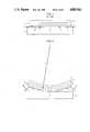
- FIG. 1is a side elevational view showing an epitaxially grown thin film semiconductor device being lifted off from an underlying single crystal substrate by the prior art etching technique.
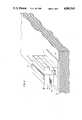
- FIG. 2is a side elevational view showing an epitaxially grown thin film semiconductor device being lifted off from an underlying single crystal substrate by the etching technique by the present invention.
- FIG. 3is a side elevational view depicting a double heterostructure test device for measuring parameters of the films obtained from the novel lift-off process.
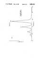
- FIG. 4shows the minority-carrier lifetime decay curve of the double heterostructure device of FIG. 3, both before and after lift-off, plotting carrier density (carriers/cm 3 ) vs. time (sec.) after application of an excitation pulse.
- FIGS. 5-7show various structures of a lifted-off semiconductor film adhered to a glass fiber in a manner so as to provide a coupled semiconductor device-fiber structure.
- FIG. 8is a pictorial illustration, partly in section, of a complete laser device bonded to a glass substrate.
- FIG. 9is a cross-sectional view of a GaAs-AlGaAs structure epitaxially regrown on a Van der Waals bonded lift-off layer.
- FIG. 10is a graph of photo-luminescence data for the structure of FIG. 9.
- FIGS. 11, 12 and 13show three embodiments of a III-V device integrated with a silicon integrated circuit and their interconnects.
- FIG. 14is a cross-sectional view of an InP-InGaAsP system double heterostructure both before lift-off and after bonding.
- FIG. 15shows the minority-carrier decay curves for the double heterostructures of FIG. 14.
- the present inventionis based upon the discovery of a unique means for lifting-off an epitaxial film from the substrate upon which it is grown so as to substantially eliminate the problem encountered in the past due to entrapment of gaseous reaction products in the channel formed during etching of a release layer between the film and the substrate.
- the present inventiondiffers from the teachings of Konagai et al by providing means for lifting the edges of the epitaxial film as the release layer is selectively etched away, thereby creating a concave film surface.
- the means provided for lifting the edges of the epitaxial filmis a support layer over the film which is applied to the film under tension causing the film to be under compression thereby creating a concave curvature in the film as the release layer is etched away.
- the inventionhas been partially described by Yablonovitch et al. in a technical article "Extreme Selectivity in the lift-off epitaxial GaAs films," Applied Physics Letters, Vol. 51, December 1987 at pages 2222-2224.
- FIG. 1which illustrates the prior art etch technique, shows a single crystal GaAs substrate 1 having a thin release film 2 on the surface thereof and epitaxially grown p-type and n-type GaAs layers 3 and 4, forming a p-n junction device, thereon.
- a support layer 5overlies the epitaxial layers 3 and 4.
- hydroflouric acidetches the release film 2 a uniformly thick channel 6 forms between the epi-layer 3 and the substrate 1.
- the gas reaction productwhich has the lowest solubility of any of the reactants or reaction products, is difficult to diffuse away thereby limiting the undercutting speed and the permissible HF acid concentration. If the solubility limits are exceeded, bubbles 7 form at the reaction zone in the channel 6 displacing the etchant and producing a gas pressure which cracks the epitaxial film.
- permissible acid concentrations and therefore etch speedsare very low.
- FIG. 2shows the results of the novel technique employing the same structure, but where a support layer 25 is applied so as to be under tension such that as undercutting of the release layer 2 occurs, the film curls with a radius of curvature R thereby forming a non-uniform channel 26 which is wider at the edges than the center of the film.
- Equating the diffusion flux with the etching flux##EQU1## where v is the etching speed, n and N are the molar concentrations of dissolved gas and release layer (e.g. AlAs) respectively, t is the thickness of the channel, D is the diffusion constant of the gas, and z is a position coordinate down the channel. It is assumed that 3 moles of gas are produced for every mole of AlAs. By making this calculation, we see that thickness cancels from both sides of the equation, hence, contrary to intuition, a thick release layer which leads to a wider channel does not overcome the mass transport problem since proportionately more gas must be removed. Integrating equation (1) down a plane parallel channel of depth L results in a maximum undercutting speed v:
- nis now the saturation solubility of the gas.
- n/Nis approximately 2 ⁇ 10 -5 and D in aqueous media is about 5 ⁇ 10 -5 cm 2 /sec.
- the speed of removal of the release layeris severely limited in channels of any significant depth.
- the channelopens up by virtue of the curvature shown in FIG. 2, then the outdiffusion becomes much easier.
- the need to transport reaction product away from the etching zoneis best satisfied by making the release layer as thin as possible.
- release layerstypically, we have employed release layers of less than 100 nm in thickness and some as thin as 2 nm.
- the epitaxial layersremain supported by the support layer and may be transferred to another substrate leaving the expensive single crystal original substrate available for re-use.
- the filmsmay be adhered to the new substrate, e.g. glass, diamond, silica, sapphire, quartz, metal, etc. by bonding the film, e.g., with an ultraviolet curable cement of the type used to splice optical fibers or, as is known in that art, with other compatible adhesives. In this way, a permanent support for large area crack free, lifted-off films can be made.
- the new substratee.g. glass, diamond, silica, sapphire, quartz, metal, etc.
- bonding the filme.g., with an ultraviolet curable cement of the type used to splice optical fibers or, as is known in that art, with other compatible adhesives.
- GaAs epitaxial filmsfor example, can be directly "optical contacted" to certain substrates, e.g. glass or silicon due to strong Van der Waals forces bonding the surfaces of the film to the substrate without the need for adhesives.
- the support layercan be washed away with an appropriate solvent.
- the minority-carrier lifetime in this structuremay be very long.
- a surface layer of Ga 1-x Al x As as thin as 10 nmis able to confine the minority-carriers within the GaAs layer 35 potential well.
- the minority-carrier lifetimebecomes very short due to the surface recombination. Therefore, the structure permits a sensitive measure of very small etch rates.
- the etch ratecan be as high as 1 mm per hour (depending upon and roughly proportional to HF acid concentration). Such a degree of selectivity ( ⁇ 10 7 ) might be associated with percolation type behavior or possibly a shift from T-point minimum to X-point minimum in the band structure.
- the release layer compositionto pure AlAs but Al x Ga 1-x As layers where x is ⁇ 0.5 were equally successful.
- the filmswere grown on ⁇ 100> oriented GaAs substrates by molecular beam epitaxy and organometallic chemical vapor deposition.
- the superb electronic quality of epitaxially grown filmsis unaffected by the lift-off process. This may be seen from the minority-carrier lifetime decay curves shown in FIG. 4. Minority-carrier lifetime is one of the best measures of crystalline perfection and purity.
- the test structure shown in FIG. 3was monitored by a contactless lifetime probe technique as is known in the art.
- the carrier density decay curvewas measured before lift-off and then again after lift-off.
- the two decay curvesoverlay identically so there is only one curve actually shown in FIG. 4. This indicates that the lift-off film did not suffer any damage or cracking with the novel process.
- the initial rapid decayis due to radiative electron-hole recombination, and the slow decay at lower density measures the Shockley-Read-Hall lifetime.
- a solutione.g., 25 grams of support layer material in 100 ml solvent is sprayed onto a finished GaAs wafer having the epitaxially grown release layer and device layers thereon through a shadow mask and the solvent is evaporated. This is done several times to build up the support layer thickness.
- a preferred support layer materialis a polymeric material known as Apiezon W which is readily soluble in trichloroethylene. This material is a mixture consisting of 62% paraffinic hydrocarbon polymer and 38% asphaltene hydrocarbons. Typically the thickness of the support layer is from 0.1 mm to 1 mm.
- the support layeris then air cured for about 1/2 hour and the wafer is then placed in an oven at about 100° C. for about 1/2 hour to cure the support layer. This heating process produces the tension which causes the curvature upon etching of the release layer.
- the epitaxial layer edges around the support layerare then exposed by removing the support layer from around the edges with a solvent and then etching non-selectively or by cleavage.
- the sampleis then placed in HF acid solution. Typically, 10% HF acid concentrations are employed, concentrated HF being a 48% solution.
- the sampleis allowed to sit in the HF for up to about 24 hours or more and the GaAs epitaxial film supported by the support layer simply floats off or is detached from the substrate. The film may then be removed and adhered to any other desired substrate.
- etching of the release layercan be enhanced if etching is accomplished at reduced temperatures, e.g. about 0° C.
- Apiezon Wis a preferred support layer which when treated as stated gives the desired result, it will be obvious to those skilled in the art that the support layer may be any polymeric material, which is cured or further cured after adhering it to the surface of the film to be removed such that the bonds formed upon curing are under tension due to adhesion to the film.
- the epitaxial film being removedmay be a single layer or multiple epitaxial layers and metallized to provide means for making electrical contact thereto and forming a semiconductor device. It should be further understood that the concept described herein is not limited to any particular semiconductor material, release layer or support layer and the principles can be employed with any compatible layers wherein a release layer can be selectively etched and undercut from between a single substrate and a overlying epitaxial semiconductor layer.
- a free epitaxial filmcomprising layers forming a light emitting diode, a laser, a photodetector or a photovoltaic device 51 may be directly adhered to an optical fiber or fiber bundle 52 as depicted in FIGS. 5-7 by means of an adhesive or by an adhesiveless optical contact using Van der Waals forces as previously described.
- Such structureswill eliminate and/or reduce the problems of optical coupling normally associated with such devices in optical systems.
- an AlGaAs laserwas grown on a GaAs substrate and then lifted off and transferred to a glass substrate.
- the finished deviceis illustrated in FIG. 8.
- the filmswere grown on the ⁇ 100> face of the GaAs substrate by organometallic chemical vapor (OMCVD) growth.
- OMCVDorganometallic chemical vapor
- the lowest layerwas a release layer 50 nm thick of n + -AlAs.
- a conductive epilayer 60 of n + -GaAswas grown to a thickness of 1.5 ⁇ m over the release layer.
- the remaining laser structurewas conventional and included a 1.5 ⁇ m n-Al 0 .3 Ga 0 .7 As waveguiding layer 62, a 0.2 ⁇ m GaAs active layer 64, a 1.5 ⁇ m p-Al 0 .3 Ga 0 .7 As waveguiding layer 66 and a 0.2 ⁇ m p + -GaAs ohmic contact layer 68.
- a channel 70was etched down to allow contact to the conductive epilayer 60.
- An n-contact 72 of Au-Ge and a p-contact 74 of Au-Tiwere deposited.
- the support layer material of Apiezon Wwas applied and then the GaAs growth substrate and the epitaxial layers were cleaved to 0.5 mm ⁇ 5 mm.
- the 0.5 mm lengthdefined the optical cavity and the 5 mm length allowed space for 5 parallel lasers.
- the individual chipswere immersed in 10% HF to dissolve the release layer and to separate the epilayers from the growth substrate.
- the Apiezon Wallowed easy handling of the separated laser layers which were then mounted on a borosilicate glass substrate 76 by a UV curable optical fiber splicing cement 78, such as Norland 61.
- the waxwas removed by trichloroethylene.
- the laserswere tested and found to have the same laser threshold current before and after lift-off.
- the use of the optical cement 78allows the adhesion of the fabricated device to almost any device substrate including SiO 2 . Van der Waals bonding of devices to substrates is generally feasible and would be particularly advantageous for device substrates having good thermal conductivity, such as diamond.
- the slight lattice mismatch between the GaAs active layer 64 and the AlGaAs waveguiding layers 62 and 66 in device of FIG. 5caused the device to be concave downward and hence difficult to Van der Waals bond. Nonetheless the desired convex curvature can be obtained by selection of relative layer thicknesses in the original laser structure.
- an epitaxial GaAs filmwas lifted off a GaAs growth substrate and Van der Waals bonded to a silicon device substrate, on which it was used as a growth substrate for further epitaxial growth.
- Molecular beam epitaxywas used to epitaxially deposit a 50 nm AlAs release layer and a 500 nm GaAs lift-off layer on a ⁇ 100> face of a GaAs growth substrate. After application of the Apiezon W support layer, the GaAs lift-off layer was lifted off with 10% HF acid at 0° C. in the procedure described before.
- the GaAs lift-off layer 80was Van der Waals bonded to a ⁇ 100> face of an n-type Si substrate 82 by the following method. With the upper surface of the lift-off layer 80 held by the Apiezon W, a tiny drop of water was applied to the lower surface. Other liquids may be substituted for the water. Handling of the Apiezon W supported the lift-off layer 80 was performed manually with polypropylene or teflon tweezers. The side of the lift-off layer 80 with the water drop was set down on the Si substrate 80. A rubber roller was rolled with hand pressure on the black wax support layer so as to push the lift-off layer 80 onto the Si substrate 82.
- the GaAs lift-off layer 82was then used as a substrate for epitaxial OMCVD growth of a GaAs-AlGaAs structure at 700° C.
- the bonded lift-off layer 80 and Si substrate 82were placed in an OMCVD reaction chamber and slowly heated to 750° C., which acted to clean the surface. Thereafter, regrowth Al 0 .48 Ga 0 .52 As layers 84 and GaAs layers 86 were grown with the thicknesses shown in FIG. 9.
- the thicknesses of the regrowth GaAs layers 86were chosen to provide energy band increases due to the narrow layers 86, which are called quantum wells in this art.
- the fabricated sample of FIG. 9was tested for photoluminescence at 5° K.
- the resultant spectrum shown in FIG. 10can be interpreted as showing layer thicknesses of 5.0, 3.8, 3.2 and 2.7 nm with relatively small layer thickness variations.
- the high quality epitaxial layers fabricated by the above processdemonstrate that more complicated structures, such as that in FIG. 8, can be grown on the lift-off layer 80 after its bonding to the Si substrate 82.
- the lift-off layer 80is of epitaxial quality and is in contact with and bonded to the Si substrate 82, it is not epitaxial to the Si substrate.
- the epitaxial filmis epitaxial with its supporting substrate. That is, the atoms of the film are in registry with the atoms of the substrate. It is inconceivable that the atoms of the lift-off layer 80 Van der Waals bonded to the device substrate 82 are in registry with the atoms thereof.
- the above-described methodprovides the only known method to contact over a larger area a crystalline thin film (defined herein as being 10 ⁇ m or less in thickness) to a substrate with which it is non-epitaxial and without the use of adhesives.
- a second pointis that the OMCVD growth was performed at a relatively high growth temperature of 700° C. Any adhesive contacting the lift-off layer to the substrate would likely degrade at these temperatures.
- a third pointis that the silicon substrate 82 of FIG. 9 could be used both for the AlGaAs regrowth and for silicon growth. Therefore, the same Si wafer can serve as a substrate for III-V devices and for Si devices grown according to standard Si technology. The most obvious combination is one part of a chip devoted to III-V opto-electronics and another part devoted to Si electronics driving the opto-electronics.
- the silicon oxide layerwould be amorphous (non-crystalline), which designation has significance only for layers of thicknesses greater than 0.3 nm.
- FIG. 11a III-V thin film device 90 integrated with a silicon microcircuit 92 on a silicon substrate 94.
- the III-V device 90may be a single device, such as the laser of FIG. 8, or a very fast integrated circuit integrated on the substrate 94 with a slower silicon integrated circuit 92.
- the silicon integrated circuit 92may be diffused or implanted into the silicon substrate 94 or may include a Si epitaxial layer grown on the Si substrate 94.
- This mixed material integrated circuitcan be fabricated in at least three different sequences.
- the completed III-V device 90can be bonded by adhesive or Van der Waals bonding to the substrate 94 after the silicon integrated circuit has been completed.
- the silicon integrated circuit 92can be grown after Van der Waals bonding of the completed III-V device 94.
- a III-V lift-off layermay be bonded to the silicon substrate 94 either before or after fabrication of the silicon integrated circuit 92, and thereafter used for growth of the III-V device.
- the Van der Waals bonding techniqueallows the production as a commodity item of silicon substrates with a III-V thin film surface bonded thereto. Such a substrate could then be stored and/or sold before further specialized processing. If the mixed material integration of FIG. 11 is then desired, the III-V material can be removed in a selected area to allow Si processing of the Si substrate but allowing III-V processing of the unremoved film.
- III-V device 90 and the silicon integrated circuitcan be accomplished in one of several ways. As illustrated in FIG. 11, n-wells 96 and p-wells 98 are formed in both the III-V device 90 and silicon integrated circuit 92, each having at the surface an alloy metal contact layer of the proper composition to form an ohmic contact with the underlying material. Two wells 96 and 98 of opposite conductivity type are then interconnected with a gold wire 100 and gold bonds 102. Alternatively, as illustrated in FIG. 12, a metallic interconnect 104 can be defined between the wells 96 and 98 by photolithography and evaporation. A buried metal contact is shown in FIG.
- n + region 106is formed from the silicon integrated circuit 92 to beneath the location of the III-V device 90.
- An alloy metal contactis formed at the surface of the n + region 106.
- a metal pad 108is deposited over the alloy metal contact. A segmented metal pad is possible for multiple contacts. Then a III-V lift-off or III-V device 90 is Van der Waals bonded to the metal pad 108.
- a fourth exampleinvolved a InGaAsP system in which InP was used as the growth substrate.
- a semi-insulating InP substrate 110was used for growth by OMCVD.
- the minority carrier lifetimewas measured with the heterostructure attached to the growth substrate 110 and found to be about 670 ns, as shown in FIG. 15.
- the previously described lift-off procedurewas then followed.
- the Apiezon Wwas applied and cured.
- the samplewas vertically cleaved to expose the AlAs release layer and was etched in 10% HF for 16 hours at 0° C. Once the heterostructure was completely undercut, it floated off and was Van der Waals bonded to a single crystal sapphire (Al 2 O 3 ) substrate 122 following the previously described bonding procedure.
- the minority carrier lifetimewas again measured with the heterostructure bonded to the sapphire device substrate 122.
- the decay ratesare the same on the growth and on the device substrate.
- the differences at densities above 10 16 cm -3have been determined to be due to inhibited spontaneous emission which is affected by nearby dielectric constants, in this case, the two different substrates.
- a particularly suitable choice for coupling with an optical fiber or alternatively, for placement on a conductive substrateis a lift-off film having a plurality of epitaxially grown doped and/or intrinsic layers of In x Ga 1-x As y P 1-y wherein x and y can vary from 0 to 1 to produce a laser device.
- Such In x Ga 1-x As y P 1-y lasersare well known in the art and are generally formed by molecular beam epitaxial growth of the layers on an InP substrate.
- a thin (2 nm-10 nm) strained AlAs release layeris employed between the substrate and the active device layers and the film is lifted-off in accordance with the teachings of the present invention.
- InGaAsPis a quaternary semiconductor and is an example of multinary semiconductor having at least two principal components.
- III-V compounds, II-VI compounds and even more general material systemsshould be usable with the lift-off and Van der Waals bonding of the invention.
- the lift-offrequires a selective etch that preferentially attacks the release layer.
- the Van der Waals bondingappears to be nearly universally applicable to substrates which are insulators, metals, any semiconductor and amorphous materials.
Landscapes
- Chemical & Material Sciences (AREA)
- Engineering & Computer Science (AREA)
- Crystallography & Structural Chemistry (AREA)
- Materials Engineering (AREA)
- Metallurgy (AREA)
- Organic Chemistry (AREA)
- Power Engineering (AREA)
- Computer Hardware Design (AREA)
- Microelectronics & Electronic Packaging (AREA)
- Chemical Kinetics & Catalysis (AREA)
- General Chemical & Material Sciences (AREA)
- Inorganic Chemistry (AREA)
- Recrystallisation Techniques (AREA)
Abstract
Description
v=Dn/3LN (2)
Claims (19)
Priority Applications (1)
| Application Number | Priority Date | Filing Date | Title |
|---|---|---|---|
| US07/279,217US4883561A (en) | 1988-03-29 | 1988-12-05 | Lift-off and subsequent bonding of epitaxial films |
Applications Claiming Priority (2)
| Application Number | Priority Date | Filing Date | Title |
|---|---|---|---|
| US07/174,852US4846931A (en) | 1988-03-29 | 1988-03-29 | Method for lifting-off epitaxial films |
| US07/279,217US4883561A (en) | 1988-03-29 | 1988-12-05 | Lift-off and subsequent bonding of epitaxial films |
Related Parent Applications (1)
| Application Number | Title | Priority Date | Filing Date |
|---|---|---|---|
| US07/174,852Continuation-In-PartUS4846931A (en) | 1988-03-29 | 1988-03-29 | Method for lifting-off epitaxial films |
Publications (1)
| Publication Number | Publication Date |
|---|---|
| US4883561Atrue US4883561A (en) | 1989-11-28 |
Family
ID=26870598
Family Applications (1)
| Application Number | Title | Priority Date | Filing Date |
|---|---|---|---|
| US07/279,217Expired - LifetimeUS4883561A (en) | 1988-03-29 | 1988-12-05 | Lift-off and subsequent bonding of epitaxial films |
Country Status (1)
| Country | Link |
|---|---|
| US (1) | US4883561A (en) |
Cited By (146)
| Publication number | Priority date | Publication date | Assignee | Title |
|---|---|---|---|---|
| WO1991017565A1 (en)* | 1990-04-30 | 1991-11-14 | Bell Communications Research, Inc. | Patterning method for epitaxial lift-off processing |
| US5073230A (en)* | 1990-04-17 | 1991-12-17 | Arizona Board Of Regents Acting On Behalf Of Arizona State University | Means and methods of lifting and relocating an epitaxial device layer |
| US5122852A (en)* | 1990-04-23 | 1992-06-16 | Bell Communications Research, Inc. | Grafted-crystal-film integrated optics and optoelectronic devices |
| WO1992012453A1 (en)* | 1990-12-31 | 1992-07-23 | Kopin Corporation | Single crystal silicon arrayed devices for display panels |
| WO1992013363A3 (en)* | 1991-01-18 | 1993-01-07 | Kopin Corp | Light emitting diode bars and arrays and method of making same |
| US5207864A (en)* | 1991-12-30 | 1993-05-04 | Bell Communications Research | Low-temperature fusion of dissimilar semiconductors |
| US5236871A (en)* | 1992-04-29 | 1993-08-17 | The United States Of America As Represented By The Administrator Of The National Aeronautics And Space Administration | Method for producing a hybridization of detector array and integrated circuit for readout |
| US5256562A (en)* | 1990-12-31 | 1993-10-26 | Kopin Corporation | Method for manufacturing a semiconductor device using a circuit transfer film |
| US5258325A (en)* | 1990-12-31 | 1993-11-02 | Kopin Corporation | Method for manufacturing a semiconductor device using a circuit transfer film |
| US5258320A (en)* | 1990-12-31 | 1993-11-02 | Kopin Corporation | Single crystal silicon arrayed devices for display panels |
| US5262347A (en)* | 1991-08-14 | 1993-11-16 | Bell Communications Research, Inc. | Palladium welding of a semiconductor body |
| US5276345A (en)* | 1992-10-30 | 1994-01-04 | California Institute Of Technology | Composite GaAs-on-quartz substrate for integration of millimeter-wave passive and active device circuitry |
| US5334283A (en)* | 1992-08-31 | 1994-08-02 | The University Of North Carolina At Chapel Hill | Process for selectively etching diamond |
| US5344517A (en)* | 1993-04-22 | 1994-09-06 | Bandgap Technology Corporation | Method for lift-off of epitaxial layers and applications thereof |
| US5362671A (en)* | 1990-12-31 | 1994-11-08 | Kopin Corporation | Method of fabricating single crystal silicon arrayed devices for display panels |
| US5376561A (en)* | 1990-12-31 | 1994-12-27 | Kopin Corporation | High density electronic circuit modules |
| US5376580A (en)* | 1993-03-19 | 1994-12-27 | Hewlett-Packard Company | Wafer bonding of light emitting diode layers |
| US5475514A (en)* | 1990-12-31 | 1995-12-12 | Kopin Corporation | Transferred single crystal arrayed devices including a light shield for projection displays |
| US5476810A (en)* | 1994-01-31 | 1995-12-19 | U.S. Philips Corporation | Manufacture of electronic devices comprising thin-film circuits using a metal foil as a temporary support |
| US5528397A (en)* | 1991-12-03 | 1996-06-18 | Kopin Corporation | Single crystal silicon transistors for display panels |
| US5528719A (en)* | 1993-10-26 | 1996-06-18 | Sumitomo Metal Mining Company Limited | Optical fiber guide structure and method of fabricating same |
| US5626921A (en)* | 1991-11-29 | 1997-05-06 | Nec Corporation | Method for forming photoluminescence layer on a semiconductor layer by ion irradiation |
| US5641381A (en)* | 1995-03-27 | 1997-06-24 | The United States Of America As Represented By The Administrator Of The National Aeronautics And Space Administration | Preferentially etched epitaxial liftoff of InP material |
| US5710057A (en)* | 1996-07-12 | 1998-01-20 | Kenney; Donald M. | SOI fabrication method |
| DE19640594A1 (en)* | 1996-10-01 | 1998-04-02 | Siemens Ag | Light-induced interface decomposition for the structuring and separation of semiconductor materials |
| US5757445A (en)* | 1990-12-31 | 1998-05-26 | Kopin Corporation | Single crystal silicon tiles for display panels |
| US5776794A (en)* | 1994-04-28 | 1998-07-07 | The Board Of Regents Of The University Of Oklahoma | Method for fabricating semiconductor laser |
| WO1998032164A1 (en)* | 1997-01-21 | 1998-07-23 | Boral Energy Limited | A method of producing thin silicon films |
| US5827751A (en)* | 1991-12-06 | 1998-10-27 | Picogiga Societe Anonyme | Method of making semiconductor components, in particular on GaAs of InP, with the substrate being recovered chemically |
| US5985742A (en)* | 1997-05-12 | 1999-11-16 | Silicon Genesis Corporation | Controlled cleavage process and device for patterned films |
| US6071795A (en)* | 1998-01-23 | 2000-06-06 | The Regents Of The University Of California | Separation of thin films from transparent substrates by selective optical processing |
| US6143582A (en)* | 1990-12-31 | 2000-11-07 | Kopin Corporation | High density electronic circuit modules |
| US6187653B1 (en) | 1999-12-17 | 2001-02-13 | Lucent Technologies, Inc. | Method for attractive bonding of two crystalline substrates |
| US6214733B1 (en) | 1999-11-17 | 2001-04-10 | Elo Technologies, Inc. | Process for lift off and handling of thin film materials |
| US6221740B1 (en) | 1999-08-10 | 2001-04-24 | Silicon Genesis Corporation | Substrate cleaving tool and method |
| US6263941B1 (en) | 1999-08-10 | 2001-07-24 | Silicon Genesis Corporation | Nozzle for cleaving substrates |
| US6284631B1 (en) | 1997-05-12 | 2001-09-04 | Silicon Genesis Corporation | Method and device for controlled cleaving process |
| US6291313B1 (en)* | 1997-05-12 | 2001-09-18 | Silicon Genesis Corporation | Method and device for controlled cleaving process |
| US6291326B1 (en) | 1998-06-23 | 2001-09-18 | Silicon Genesis Corporation | Pre-semiconductor process implant and post-process film separation |
| US6312304B1 (en) | 1998-12-15 | 2001-11-06 | E Ink Corporation | Assembly of microencapsulated electronic displays |
| US20020028314A1 (en)* | 1994-01-27 | 2002-03-07 | Tischler Michael A. | Bulk single crystal gallium nitride and method of making same |
| NL1016431C2 (en)* | 2000-10-18 | 2002-04-22 | Univ Nijmegen | Method for separating a film and a substrate. |
| EP1202327A1 (en)* | 2000-10-31 | 2002-05-02 | Disco Corporation | Semiconductor device |
| US20020098426A1 (en)* | 2000-07-16 | 2002-07-25 | Sreenivasan S. V. | High-resolution overlay alignment methods and systems for imprint lithography |
| US6436614B1 (en) | 2000-10-20 | 2002-08-20 | Feng Zhou | Method for the formation of a thin optical crystal layer overlying a low dielectric constant substrate |
| US6445489B1 (en) | 1998-03-18 | 2002-09-03 | E Ink Corporation | Electrophoretic displays and systems for addressing such displays |
| US6473072B1 (en) | 1998-05-12 | 2002-10-29 | E Ink Corporation | Microencapsulated electrophoretic electrostatically-addressed media for drawing device applications |
| US20020171080A1 (en)* | 2001-05-18 | 2002-11-21 | Faris Sadeg M. | Thin films and production methods thereof |
| US6498114B1 (en) | 1999-04-09 | 2002-12-24 | E Ink Corporation | Method for forming a patterned semiconductor film |
| US6500732B1 (en) | 1999-08-10 | 2002-12-31 | Silicon Genesis Corporation | Cleaving process to fabricate multilayered substrates using low implantation doses |
| US6504524B1 (en) | 2000-03-08 | 2003-01-07 | E Ink Corporation | Addressing methods for displays having zero time-average field |
| US6518949B2 (en) | 1998-04-10 | 2003-02-11 | E Ink Corporation | Electronic displays using organic-based field effect transistors |
| US6531997B1 (en) | 1999-04-30 | 2003-03-11 | E Ink Corporation | Methods for addressing electrophoretic displays |
| US6548382B1 (en) | 1997-07-18 | 2003-04-15 | Silicon Genesis Corporation | Gettering technique for wafers made using a controlled cleaving process |
| US6593978B2 (en) | 1990-12-31 | 2003-07-15 | Kopin Corporation | Method for manufacturing active matrix liquid crystal displays |
| US20030162312A1 (en)* | 2001-11-30 | 2003-08-28 | Semiconductor Energy Laboratory Co., Ltd. | Vehicle, display device and manufacturing method for a semiconductor device |
| US6627953B1 (en) | 1990-12-31 | 2003-09-30 | Kopin Corporation | High density electronic circuit modules |
| US6627518B1 (en)* | 1998-02-27 | 2003-09-30 | Seiko Epson Corporation | Method for making three-dimensional device |
| US20030206675A1 (en)* | 2002-05-03 | 2003-11-06 | Fujitsu Limited | Thin film electro-optical deflector device and a method of fabrication of such a device |
| US6669801B2 (en)* | 2000-01-21 | 2003-12-30 | Fujitsu Limited | Device transfer method |
| US6677249B2 (en)* | 1998-01-27 | 2004-01-13 | Robert Bosch Gmbh | Method for manufacturing breakaway layers for detaching deposited layer systems |
| US6683333B2 (en) | 2000-07-14 | 2004-01-27 | E Ink Corporation | Fabrication of electronic circuit elements using unpatterned semiconductor layers |
| US20040021254A1 (en)* | 2002-08-01 | 2004-02-05 | Sreenivasan Sidlgata V. | Alignment methods for imprint lithography |
| US20040206371A1 (en)* | 1996-09-30 | 2004-10-21 | Bran Mario E. | Wafer cleaning |
| US6825068B2 (en) | 2000-04-18 | 2004-11-30 | E Ink Corporation | Process for fabricating thin film transistors |
| US20040253794A1 (en)* | 2001-05-18 | 2004-12-16 | Faris Sadeg M. | MEMS and method of manufacturing MEMS |
| US6839158B2 (en) | 1997-08-28 | 2005-01-04 | E Ink Corporation | Encapsulated electrophoretic displays having a monolayer of capsules and materials and methods for making the same |
| US6842657B1 (en) | 1999-04-09 | 2005-01-11 | E Ink Corporation | Reactive formation of dielectric layers and protection of organic layers in organic semiconductor device fabrication |
| US20050079664A1 (en)* | 2001-09-12 | 2005-04-14 | Faris Sadeg M. | Method of fabricating multi layer devices on buried oxide layer substrates |
| US20050104163A1 (en)* | 2001-11-29 | 2005-05-19 | Weber Klaus J. | Semiconductor texturing process |
| US20050112848A1 (en)* | 2001-09-12 | 2005-05-26 | Reveo, Inc. | Method of fabricating vertical integrated circuits |
| US6900851B2 (en) | 2002-02-08 | 2005-05-31 | E Ink Corporation | Electro-optic displays and optical systems for addressing such displays |
| US20050164470A1 (en)* | 2001-12-28 | 2005-07-28 | Semiconductor Energy Laboratory Co., Ltd., A Japan Corporation | Method for fabricating a semiconductor device by transferring a layer to a support with curvature |
| US6929762B2 (en) | 2002-11-13 | 2005-08-16 | Molecular Imprints, Inc. | Method of reducing pattern distortions during imprint lithography processes |
| US20050227455A1 (en)* | 2004-03-29 | 2005-10-13 | Jongkook Park | Method of separating layers of material |
| US6967640B2 (en) | 2001-07-27 | 2005-11-22 | E Ink Corporation | Microencapsulated electrophoretic display with integrated driver |
| US20050272225A1 (en)* | 2000-11-29 | 2005-12-08 | Origin Energy Solar Pty Ltd. | Semiconductor processing |
| US6990870B2 (en) | 2002-12-12 | 2006-01-31 | Molecular Imprints, Inc. | System for determining characteristics of substrates employing fluid geometries |
| US20060073978A1 (en)* | 2003-02-06 | 2006-04-06 | Brown University | Method and apparatus for making continuous films of a single crystal material |
| US7030412B1 (en) | 1999-05-05 | 2006-04-18 | E Ink Corporation | Minimally-patterned semiconductor devices for display applications |
| US7056808B2 (en) | 1999-08-10 | 2006-06-06 | Silicon Genesis Corporation | Cleaving process to fabricate multilayered substrates using low implantation doses |
| US20060134893A1 (en)* | 2004-12-16 | 2006-06-22 | Savage Donald E | Fabrication of strained heterojunction structures |
| US7077992B2 (en) | 2002-07-11 | 2006-07-18 | Molecular Imprints, Inc. | Step and repeat imprint lithography processes |
| US7122079B2 (en) | 2004-02-27 | 2006-10-17 | Molecular Imprints, Inc. | Composition for an etching mask comprising a silicon-containing material |
| US7136150B2 (en) | 2003-09-25 | 2006-11-14 | Molecular Imprints, Inc. | Imprint lithography template having opaque alignment marks |
| US7157036B2 (en) | 2003-06-17 | 2007-01-02 | Molecular Imprints, Inc | Method to reduce adhesion between a conformable region and a pattern of a mold |
| US7176880B2 (en) | 1999-07-21 | 2007-02-13 | E Ink Corporation | Use of a storage capacitor to enhance the performance of an active matrix driven electronic display |
| US20070105339A1 (en)* | 2001-09-12 | 2007-05-10 | Faris Sadeg M | Method of fabricating multi layer MEMS and microfluidic devices |
| US7242513B2 (en) | 1997-08-28 | 2007-07-10 | E Ink Corporation | Encapsulated electrophoretic displays having a monolayer of capsules and materials and methods for making the same |
| US20070196586A1 (en)* | 2003-06-26 | 2007-08-23 | Nikon Corporation | Method for producing multilayer optical device |
| US20070284688A1 (en)* | 2006-06-13 | 2007-12-13 | Wisconsin Alumni Research Foundation | Pin diodes for photodetection and high-speed, high-resolution image sensing |
| US7361574B1 (en) | 2006-11-17 | 2008-04-22 | Sharp Laboratories Of America, Inc | Single-crystal silicon-on-glass from film transfer |
| US20080097065A1 (en)* | 2004-02-27 | 2008-04-24 | Molecular Imprints, Inc. | Composition for an etching mask comprising a silicon-containing material |
| US7442957B2 (en) | 2001-08-01 | 2008-10-28 | Semiconductor Energy Laboratory Co., Ltd. | Semiconductor device and manufacturing method thereof |
| US7452574B2 (en) | 2003-02-27 | 2008-11-18 | Molecular Imprints, Inc. | Method to reduce adhesion between a polymerizable layer and a substrate employing a fluorine-containing layer |
| US20090321886A1 (en)* | 2008-05-30 | 2009-12-31 | Alta Devices, Inc. | Epitaxial lift off stack having a unidirectionally shrunk handle and methods thereof |
| US20090324379A1 (en)* | 2008-05-30 | 2009-12-31 | Alta Devices, Inc. | Methods and apparatus for a chemical vapor deposition reactor |
| US20100047959A1 (en)* | 2006-08-07 | 2010-02-25 | Emcore Solar Power, Inc. | Epitaxial Lift Off on Film Mounted Inverted Metamorphic Multijunction Solar Cells |
| US20100078722A1 (en)* | 2006-09-08 | 2010-04-01 | Zhenqiang Ma | Method for fabricating high-speed thin-film transistors |
| US20100116784A1 (en)* | 2008-10-10 | 2010-05-13 | Alta Devices, Inc. | Mesa etch method and composition for epitaxial lift off |
| US20100120233A1 (en)* | 2008-10-10 | 2010-05-13 | Alta Devices, Inc. | Continuous Feed Chemical Vapor Deposition |
| US20100151689A1 (en)* | 2008-12-17 | 2010-06-17 | Alta Devices, Inc. | Tape-based epitaxial lift off apparatuses and methods |
| US20100147370A1 (en)* | 2008-12-08 | 2010-06-17 | Alta Devices, Inc. | Multiple stack deposition for epitaxial lift off |
| US20100203730A1 (en)* | 2009-02-09 | 2010-08-12 | Emcore Solar Power, Inc. | Epitaxial Lift Off in Inverted Metamorphic Multijunction Solar Cells |
| US7776717B2 (en) | 1997-05-12 | 2010-08-17 | Silicon Genesis Corporation | Controlled process and resulting device |
| CN1577905B (en)* | 2003-06-25 | 2010-08-25 | 日本冲信息株式会社 | Method for producing semiconductor device |
| US7803308B2 (en) | 2005-12-01 | 2010-09-28 | Molecular Imprints, Inc. | Technique for separating a mold from solidified imprinting material |
| US7811900B2 (en) | 2006-09-08 | 2010-10-12 | Silicon Genesis Corporation | Method and structure for fabricating solar cells using a thick layer transfer process |
| US7893435B2 (en) | 2000-04-18 | 2011-02-22 | E Ink Corporation | Flexible electronic circuits and displays including a backplane comprising a patterned metal foil having a plurality of apertures extending therethrough |
| US20110083601A1 (en)* | 2009-10-14 | 2011-04-14 | Alta Devices, Inc. | High growth rate deposition for group iii/v materials |
| US20110108097A1 (en)* | 2009-11-06 | 2011-05-12 | Alliance For Sustainable Energy, Llc | Methods of manipulating stressed epistructures |
| US20110136296A1 (en)* | 2009-12-07 | 2011-06-09 | Electronics And Telecommunications Research Institute | Method for manufacturing semiconductor device |
| US20110146791A1 (en)* | 2008-08-21 | 2011-06-23 | Alliance For Sustainable Energy, Llc | Epitaxial growth of silicon for layer transfer |
| WO2011137508A1 (en)* | 2010-05-05 | 2011-11-10 | National Research Council Of Canada | Asphaltene components as organic electronic materials |
| US8076386B2 (en) | 2004-02-23 | 2011-12-13 | Molecular Imprints, Inc. | Materials for imprint lithography |
| US20120062880A1 (en)* | 2010-09-10 | 2012-03-15 | Hon Hai Precision Industry Co., Ltd. | Optical fiber probe and raman detecting system having same |
| US8187377B2 (en) | 2002-10-04 | 2012-05-29 | Silicon Genesis Corporation | Non-contact etch annealing of strained layers |
| US8293619B2 (en) | 2008-08-28 | 2012-10-23 | Silicon Genesis Corporation | Layer transfer of films utilizing controlled propagation |
| US20120276676A1 (en)* | 2009-02-09 | 2012-11-01 | Emcore Solar Power, Inc. | Epitaxial lift off in inverted metamorphic multijunction solar cells |
| US8329557B2 (en) | 2009-05-13 | 2012-12-11 | Silicon Genesis Corporation | Techniques for forming thin films by implantation with reduced channeling |
| US8330126B2 (en) | 2008-08-25 | 2012-12-11 | Silicon Genesis Corporation | Race track configuration and method for wafering silicon solar substrates |
| US8349241B2 (en) | 2002-10-04 | 2013-01-08 | Molecular Imprints, Inc. | Method to arrange features on a substrate to replicate features having minimal dimensional variability |
| US20130023075A1 (en)* | 2011-07-21 | 2013-01-24 | Lg Display Co., Ltd. | Method of Forming Process Substrate Using Thin Glass Substrate and Method of Fabricating Flat Display Device Using the Same |
| US8362592B2 (en) | 2009-02-27 | 2013-01-29 | Alta Devices Inc. | Tiled substrates for deposition and epitaxial lift off processes |
| WO2013028525A1 (en)* | 2011-08-19 | 2013-02-28 | Hunt Energy Iq, Lp | Methods and apparatus using asphaltenes in solid-state organic solar cells |
| EP2618385A1 (en) | 2012-01-20 | 2013-07-24 | AZUR SPACE Solar Power GmbH | Semi-finished product of a multiple solar cell and method for manufacturing a multiple solar cell |
| WO2013184638A3 (en)* | 2012-06-04 | 2014-02-20 | The Regents Of The University Of Michigan | Strain control for acceleration of epitaxial lift-off |
| US8748324B1 (en) | 2013-02-26 | 2014-06-10 | The Boeing Company | Systems and methods for separating components of a multilayer stack of electronic components |
| US8889909B2 (en) | 2013-03-15 | 2014-11-18 | Hunt Energy Enterprises, Llc | Tunable photoactive compounds |
| US8941147B2 (en) | 2012-10-03 | 2015-01-27 | International Business Machines Corporation | Transistor formation using cold welding |
| CN104377301A (en)* | 2014-11-24 | 2015-02-25 | 苏州矩阵光电有限公司 | III-V group compound semiconductor Hall element and manufacturing method thereof |
| US8993410B2 (en) | 2006-09-08 | 2015-03-31 | Silicon Genesis Corporation | Substrate cleaving under controlled stress conditions |
| US20150325465A1 (en)* | 2014-05-08 | 2015-11-12 | Tokyo Ohka Kogyo Co., Ltd. | Supporting member separation method |
| WO2015194721A1 (en)* | 2014-06-20 | 2015-12-23 | 한국기계연구원 | Method of forming quantum dot thin film |
| US9223202B2 (en) | 2000-07-17 | 2015-12-29 | Board Of Regents, The University Of Texas System | Method of automatic fluid dispensing for imprint lithography processes |
| US9340895B1 (en) | 2013-06-27 | 2016-05-17 | The Boeing Company | Systems and methods for separating components of a multilayer stack of electronic components |
| US9362439B2 (en) | 2008-05-07 | 2016-06-07 | Silicon Genesis Corporation | Layer transfer of films utilizing controlled shear region |
| US9947568B2 (en) | 2013-02-20 | 2018-04-17 | Semiconductor Energy Laboratory Co., Ltd. | Peeling method, semiconductor device, and peeling apparatus |
| US10189048B2 (en) | 2013-12-12 | 2019-01-29 | Semiconductor Energy Laboratory Co., Ltd. | Peeling method and peeling apparatus |
| US10242915B2 (en) | 2017-02-21 | 2019-03-26 | Fraunhofer-Gesellschaft zur Förderung der angewandten Forschung e.V. | Method for transferring at least one thin film |
| US10367332B2 (en) | 2015-10-08 | 2019-07-30 | Samsung Electronics Co., Ltd. | Edge emitting laser light source and 3D image obtaining apparatus including the same |
| WO2019180165A1 (en) | 2018-03-22 | 2019-09-26 | Iee International Electronics & Engineering S.A. | Photodetector |
| WO2020095610A1 (en)* | 2018-11-06 | 2020-05-14 | 信越半導体株式会社 | Method for manufacturing semiconductor substrate for light-emitting element, and method for manufacturing light-emitting element |
| US10852492B1 (en)* | 2014-10-29 | 2020-12-01 | Acacia Communications, Inc. | Techniques to combine two integrated photonic substrates |
| JPWO2021044617A1 (en)* | 2019-09-06 | 2021-03-11 | ||
| US11393683B2 (en) | 2009-10-14 | 2022-07-19 | Utica Leaseco, Llc | Methods for high growth rate deposition for forming different cells on a wafer |
- 1988
- 1988-12-05USUS07/279,217patent/US4883561A/ennot_activeExpired - Lifetime
Non-Patent Citations (12)
| Title |
|---|
| D. L. Miller et al., "GaAs Peeled Film Solar Cells," Document #MRDC41056.49 FRD, Final Report Draft for the Period Mar. 15, 1980-Dec. 31, 1981, Prepared for Solar Energy Research Institute Under Subcontract No. X5-0-9002-2. |
| D. L. Miller et al., GaAs Peeled Film Solar Cells, Document MRDC41056.49 FRD, Final Report Draft for the Period Mar. 15, 1980 Dec. 31, 1981, Prepared for Solar Energy Research Institute Under Subcontract No. X5 0 9002 2.* |
| J. C. C. Fan, "Thin Films of III-V Compounds and Their Applications," Journal de Physique Colloquium, 43, Cl, 327-339 (1982). |
| J. C. C. Fan, Thin Films of III V Compounds and Their Applications, Journal de Physique Colloquium, 43, Cl, 327 339 (1982).* |
| K. Y. Lee et al., "Fabrication of Ultrasmall Devices on Thin Active GaAs Membrane," Journal of Vacuum Science Technology B5(1), 322-325, Jan./Feb. (1987). |
| K. Y. Lee et al., Fabrication of Ultrasmall Devices on Thin Active GaAs Membrane, Journal of Vacuum Science Technology B5(1), 322 325, Jan./Feb. (1987).* |
| Klem et al., "Characteristics of Lift-Off Fabricated AlGaAs/InGaAs Single-Strained Quantum Well Structures on Glass and Silicon Substrates" Preprint Article, Sandia National Laboratories, Albuquerque, N.M., pp. 1-6. |
| Klem et al., Characteristics of Lift Off Fabricated AlGaAs/InGaAs Single Strained Quantum Well Structures on Glass and Silicon Substrates Preprint Article, Sandia National Laboratories, Albuquerque, N.M., pp. 1 6.* |
| M. Konagai et al., "High Efficiency GaAs Thin Film Solar Cells by Peeled Film Technology," Journal of Crystal Growth, 45, pp. 277-280 (1978). |
| M. Konagai et al., High Efficiency GaAs Thin Film Solar Cells by Peeled Film Technology, Journal of Crystal Growth, 45, pp. 277 280 (1978).* |
| Yablonovitch et al., "Extreme Selectivity in the Lift-Off of Epitaxial GaAs Films", Applied Physics Letters, 51(26), 2222-2224 (Dec. 28, 1987). |
| Yablonovitch et al., Extreme Selectivity in the Lift Off of Epitaxial GaAs Films , Applied Physics Letters, 51(26), 2222 2224 (Dec. 28, 1987).* |
Cited By (296)
| Publication number | Priority date | Publication date | Assignee | Title |
|---|---|---|---|---|
| US5073230A (en)* | 1990-04-17 | 1991-12-17 | Arizona Board Of Regents Acting On Behalf Of Arizona State University | Means and methods of lifting and relocating an epitaxial device layer |
| US5122852A (en)* | 1990-04-23 | 1992-06-16 | Bell Communications Research, Inc. | Grafted-crystal-film integrated optics and optoelectronic devices |
| US5201996A (en)* | 1990-04-30 | 1993-04-13 | Bell Communications Research, Inc. | Patterning method for epitaxial lift-off processing |
| WO1991017565A1 (en)* | 1990-04-30 | 1991-11-14 | Bell Communications Research, Inc. | Patterning method for epitaxial lift-off processing |
| JPH05506542A (en)* | 1990-04-30 | 1993-09-22 | ベル コミュニケーションズ リサーチ インコーポレーテッド | Patterning method in epitaxial lift-off process |
| US6919935B2 (en) | 1990-12-31 | 2005-07-19 | Kopin Corporation | Method of forming an active matrix display |
| US5757445A (en)* | 1990-12-31 | 1998-05-26 | Kopin Corporation | Single crystal silicon tiles for display panels |
| US6627953B1 (en) | 1990-12-31 | 2003-09-30 | Kopin Corporation | High density electronic circuit modules |
| US6593978B2 (en) | 1990-12-31 | 2003-07-15 | Kopin Corporation | Method for manufacturing active matrix liquid crystal displays |
| US6143582A (en)* | 1990-12-31 | 2000-11-07 | Kopin Corporation | High density electronic circuit modules |
| US5256562A (en)* | 1990-12-31 | 1993-10-26 | Kopin Corporation | Method for manufacturing a semiconductor device using a circuit transfer film |
| US5258325A (en)* | 1990-12-31 | 1993-11-02 | Kopin Corporation | Method for manufacturing a semiconductor device using a circuit transfer film |
| US5258320A (en)* | 1990-12-31 | 1993-11-02 | Kopin Corporation | Single crystal silicon arrayed devices for display panels |
| US6232136B1 (en) | 1990-12-31 | 2001-05-15 | Kopin Corporation | Method of transferring semiconductors |
| US6521940B1 (en) | 1990-12-31 | 2003-02-18 | Kopin Corporation | High density electronic circuit modules |
| US5702963A (en)* | 1990-12-31 | 1997-12-30 | Kopin Corporation | Method of forming high density electronic circuit modules |
| US5539550A (en)* | 1990-12-31 | 1996-07-23 | Kopin Corporation | Liquid crystal display having adhered circuit tiles |
| US6486929B1 (en) | 1990-12-31 | 2002-11-26 | Kopin Corporation | Bonded layer semiconductor device |
| WO1992012453A1 (en)* | 1990-12-31 | 1992-07-23 | Kopin Corporation | Single crystal silicon arrayed devices for display panels |
| US5362671A (en)* | 1990-12-31 | 1994-11-08 | Kopin Corporation | Method of fabricating single crystal silicon arrayed devices for display panels |
| US5377031A (en)* | 1990-12-31 | 1994-12-27 | Kopin Corporation | Single crystal silicon tiles for liquid crystal display panels including light shielding layers |
| US5376561A (en)* | 1990-12-31 | 1994-12-27 | Kopin Corporation | High density electronic circuit modules |
| US6424020B1 (en) | 1990-12-31 | 2002-07-23 | Kopin Corporation | High Density electronic circuit modules |
| US6317175B1 (en)* | 1990-12-31 | 2001-11-13 | Kopin Corporation | Single crystal silicon arrayed devices with optical shield between transistor and substrate |
| US5475514A (en)* | 1990-12-31 | 1995-12-12 | Kopin Corporation | Transferred single crystal arrayed devices including a light shield for projection displays |
| US6414783B2 (en) | 1990-12-31 | 2002-07-02 | Kopin Corporation | Method of transferring semiconductors |
| US20040070697A1 (en)* | 1990-12-31 | 2004-04-15 | Kopin Corporation | Method of forming an active matrix display |
| US5206749A (en)* | 1990-12-31 | 1993-04-27 | Kopin Corporation | Liquid crystal display having essentially single crystal transistors pixels and driving circuits |
| US6403985B1 (en)* | 1991-01-18 | 2002-06-11 | Kopin Corporation | Method of making light emitting diode displays |
| US5453405A (en)* | 1991-01-18 | 1995-09-26 | Kopin Corporation | Method of making light emitting diode bars and arrays |
| US5300788A (en)* | 1991-01-18 | 1994-04-05 | Kopin Corporation | Light emitting diode bars and arrays and method of making same |
| WO1992013363A3 (en)* | 1991-01-18 | 1993-01-07 | Kopin Corp | Light emitting diode bars and arrays and method of making same |
| US5262347A (en)* | 1991-08-14 | 1993-11-16 | Bell Communications Research, Inc. | Palladium welding of a semiconductor body |
| US5626921A (en)* | 1991-11-29 | 1997-05-06 | Nec Corporation | Method for forming photoluminescence layer on a semiconductor layer by ion irradiation |
| US5528397A (en)* | 1991-12-03 | 1996-06-18 | Kopin Corporation | Single crystal silicon transistors for display panels |
| US5827751A (en)* | 1991-12-06 | 1998-10-27 | Picogiga Societe Anonyme | Method of making semiconductor components, in particular on GaAs of InP, with the substrate being recovered chemically |
| US5207864A (en)* | 1991-12-30 | 1993-05-04 | Bell Communications Research | Low-temperature fusion of dissimilar semiconductors |
| US5236871A (en)* | 1992-04-29 | 1993-08-17 | The United States Of America As Represented By The Administrator Of The National Aeronautics And Space Administration | Method for producing a hybridization of detector array and integrated circuit for readout |
| US5334283A (en)* | 1992-08-31 | 1994-08-02 | The University Of North Carolina At Chapel Hill | Process for selectively etching diamond |
| US5276345A (en)* | 1992-10-30 | 1994-01-04 | California Institute Of Technology | Composite GaAs-on-quartz substrate for integration of millimeter-wave passive and active device circuitry |
| US5376580A (en)* | 1993-03-19 | 1994-12-27 | Hewlett-Packard Company | Wafer bonding of light emitting diode layers |
| US5344517A (en)* | 1993-04-22 | 1994-09-06 | Bandgap Technology Corporation | Method for lift-off of epitaxial layers and applications thereof |
| WO1994024341A1 (en)* | 1993-04-22 | 1994-10-27 | Bandgap Technology Corporation | Improved method for lift-off of epitaxial layers |
| US5528719A (en)* | 1993-10-26 | 1996-06-18 | Sumitomo Metal Mining Company Limited | Optical fiber guide structure and method of fabricating same |
| US7794542B2 (en) | 1994-01-27 | 2010-09-14 | Cree, Inc. | Bulk single crystal gallium nitride and method of making same |
| US20020028314A1 (en)* | 1994-01-27 | 2002-03-07 | Tischler Michael A. | Bulk single crystal gallium nitride and method of making same |
| US6972051B2 (en)* | 1994-01-27 | 2005-12-06 | Cree, Inc. | Bulk single crystal gallium nitride and method of making same |
| US20080127884A1 (en)* | 1994-01-27 | 2008-06-05 | Cree, Inc. | Bulk single crystal gallium nitride and method of making same |
| US7332031B2 (en) | 1994-01-27 | 2008-02-19 | Cree, Inc. | Bulk single crystal gallium nitride and method of making same |
| US5476810A (en)* | 1994-01-31 | 1995-12-19 | U.S. Philips Corporation | Manufacture of electronic devices comprising thin-film circuits using a metal foil as a temporary support |
| US5776794A (en)* | 1994-04-28 | 1998-07-07 | The Board Of Regents Of The University Of Oklahoma | Method for fabricating semiconductor laser |
| US5641381A (en)* | 1995-03-27 | 1997-06-24 | The United States Of America As Represented By The Administrator Of The National Aeronautics And Space Administration | Preferentially etched epitaxial liftoff of InP material |
| US5710057A (en)* | 1996-07-12 | 1998-01-20 | Kenney; Donald M. | SOI fabrication method |
| US20040206371A1 (en)* | 1996-09-30 | 2004-10-21 | Bran Mario E. | Wafer cleaning |
| DE19640594A1 (en)* | 1996-10-01 | 1998-04-02 | Siemens Ag | Light-induced interface decomposition for the structuring and separation of semiconductor materials |
| US7341925B2 (en) | 1996-10-01 | 2008-03-11 | Osram Gmbh | Method for transferring a semiconductor body from a growth substrate to a support material |
| US7713840B2 (en) | 1996-10-01 | 2010-05-11 | Osram Gmbh | Electronic components produced by a method of separating two layers of material from one another |
| US6974758B2 (en) | 1996-10-01 | 2005-12-13 | Siemens Aktiengesellschaft | Method of producing a light-emitting diode |
| US20060040468A1 (en)* | 1996-10-01 | 2006-02-23 | Siemens Aktiengesellschaft | Method for transferring a semiconductor body from a growth substrate to a support material |
| US6559075B1 (en) | 1996-10-01 | 2003-05-06 | Siemens Aktiengesellschaft | Method of separating two layers of material from one another and electronic components produced using this process |
| DE19640594B4 (en)* | 1996-10-01 | 2016-08-04 | Osram Gmbh | module |
| US6740604B2 (en) | 1996-10-01 | 2004-05-25 | Siemens Aktiengesellschaft | Method of separating two layers of material from one another |
| US20040072382A1 (en)* | 1996-10-01 | 2004-04-15 | Siemens Aktiengesellschaft | Method of producing a light-emitting diode |
| US20080164571A1 (en)* | 1996-10-01 | 2008-07-10 | Osram Gmbh | Electronic components produced by a method of separating two layers of material from one another |
| WO1998032164A1 (en)* | 1997-01-21 | 1998-07-23 | Boral Energy Limited | A method of producing thin silicon films |
| US7160790B2 (en) | 1997-05-12 | 2007-01-09 | Silicon Genesis Corporation | Controlled cleaving process |
| US6162705A (en)* | 1997-05-12 | 2000-12-19 | Silicon Genesis Corporation | Controlled cleavage process and resulting device using beta annealing |
| US7410887B2 (en) | 1997-05-12 | 2008-08-12 | Silicon Genesis Corporation | Controlled process and resulting device |
| US7371660B2 (en) | 1997-05-12 | 2008-05-13 | Silicon Genesis Corporation | Controlled cleaving process |
| US6294814B1 (en) | 1997-05-12 | 2001-09-25 | Silicon Genesis Corporation | Cleaved silicon thin film with rough surface |
| US7348258B2 (en) | 1997-05-12 | 2008-03-25 | Silicon Genesis Corporation | Method and device for controlled cleaving process |
| US6291313B1 (en)* | 1997-05-12 | 2001-09-18 | Silicon Genesis Corporation | Method and device for controlled cleaving process |
| US5985742A (en)* | 1997-05-12 | 1999-11-16 | Silicon Genesis Corporation | Controlled cleavage process and device for patterned films |
| US6458672B1 (en) | 1997-05-12 | 2002-10-01 | Silicon Genesis Corporation | Controlled cleavage process and resulting device using beta annealing |
| US6290804B1 (en) | 1997-05-12 | 2001-09-18 | Silicon Genesis Corporation | Controlled cleavage process using patterning |
| US6284631B1 (en) | 1997-05-12 | 2001-09-04 | Silicon Genesis Corporation | Method and device for controlled cleaving process |
| US6245161B1 (en) | 1997-05-12 | 2001-06-12 | Silicon Genesis Corporation | Economical silicon-on-silicon hybrid wafer assembly |
| US6486041B2 (en) | 1997-05-12 | 2002-11-26 | Silicon Genesis Corporation | Method and device for controlled cleaving process |
| US6010579A (en)* | 1997-05-12 | 2000-01-04 | Silicon Genesis Corporation | Reusable substrate for thin film separation |
| US7759217B2 (en) | 1997-05-12 | 2010-07-20 | Silicon Genesis Corporation | Controlled process and resulting device |
| US6187110B1 (en) | 1997-05-12 | 2001-02-13 | Silicon Genesis Corporation | Device for patterned films |
| US6511899B1 (en) | 1997-05-12 | 2003-01-28 | Silicon Genesis Corporation | Controlled cleavage process using pressurized fluid |
| US7776717B2 (en) | 1997-05-12 | 2010-08-17 | Silicon Genesis Corporation | Controlled process and resulting device |
| US6790747B2 (en) | 1997-05-12 | 2004-09-14 | Silicon Genesis Corporation | Method and device for controlled cleaving process |
| US6391740B1 (en) | 1997-05-12 | 2002-05-21 | Silicon Genesis Corporation | Generic layer transfer methodology by controlled cleavage process |
| US6528391B1 (en) | 1997-05-12 | 2003-03-04 | Silicon Genesis, Corporation | Controlled cleavage process and device for patterned films |
| US6159825A (en)* | 1997-05-12 | 2000-12-12 | Silicon Genesis Corporation | Controlled cleavage thin film separation process using a reusable substrate |
| US6048411A (en)* | 1997-05-12 | 2000-04-11 | Silicon Genesis Corporation | Silicon-on-silicon hybrid wafer assembly |
| US7846818B2 (en) | 1997-05-12 | 2010-12-07 | Silicon Genesis Corporation | Controlled process and resulting device |
| US6558802B1 (en) | 1997-05-12 | 2003-05-06 | Silicon Genesis Corporation | Silicon-on-silicon hybrid wafer assembly |
| US6159824A (en)* | 1997-05-12 | 2000-12-12 | Silicon Genesis Corporation | Silicon-on-silicon wafer bonding process using a thin film blister-separation method |
| US6155909A (en)* | 1997-05-12 | 2000-12-05 | Silicon Genesis Corporation | Controlled cleavage system using pressurized fluid |
| US6632724B2 (en) | 1997-05-12 | 2003-10-14 | Silicon Genesis Corporation | Controlled cleaving process |
| US6146979A (en)* | 1997-05-12 | 2000-11-14 | Silicon Genesis Corporation | Pressurized microbubble thin film separation process using a reusable substrate |
| US6890838B2 (en) | 1997-07-18 | 2005-05-10 | Silicon Genesis Corporation | Gettering technique for wafers made using a controlled cleaving process |
| US6548382B1 (en) | 1997-07-18 | 2003-04-15 | Silicon Genesis Corporation | Gettering technique for wafers made using a controlled cleaving process |
| US6839158B2 (en) | 1997-08-28 | 2005-01-04 | E Ink Corporation | Encapsulated electrophoretic displays having a monolayer of capsules and materials and methods for making the same |
| US7242513B2 (en) | 1997-08-28 | 2007-07-10 | E Ink Corporation | Encapsulated electrophoretic displays having a monolayer of capsules and materials and methods for making the same |
| US6071795A (en)* | 1998-01-23 | 2000-06-06 | The Regents Of The University Of California | Separation of thin films from transparent substrates by selective optical processing |
| US6677249B2 (en)* | 1998-01-27 | 2004-01-13 | Robert Bosch Gmbh | Method for manufacturing breakaway layers for detaching deposited layer systems |
| US6627518B1 (en)* | 1998-02-27 | 2003-09-30 | Seiko Epson Corporation | Method for making three-dimensional device |
| US6445489B1 (en) | 1998-03-18 | 2002-09-03 | E Ink Corporation | Electrophoretic displays and systems for addressing such displays |
| US6518949B2 (en) | 1998-04-10 | 2003-02-11 | E Ink Corporation | Electronic displays using organic-based field effect transistors |
| US6473072B1 (en) | 1998-05-12 | 2002-10-29 | E Ink Corporation | Microencapsulated electrophoretic electrostatically-addressed media for drawing device applications |
| US6738050B2 (en) | 1998-05-12 | 2004-05-18 | E Ink Corporation | Microencapsulated electrophoretic electrostatically addressed media for drawing device applications |
| US6291326B1 (en) | 1998-06-23 | 2001-09-18 | Silicon Genesis Corporation | Pre-semiconductor process implant and post-process film separation |
| US6312304B1 (en) | 1998-12-15 | 2001-11-06 | E Ink Corporation | Assembly of microencapsulated electronic displays |
| US6842657B1 (en) | 1999-04-09 | 2005-01-11 | E Ink Corporation | Reactive formation of dielectric layers and protection of organic layers in organic semiconductor device fabrication |
| US6498114B1 (en) | 1999-04-09 | 2002-12-24 | E Ink Corporation | Method for forming a patterned semiconductor film |
| US6531997B1 (en) | 1999-04-30 | 2003-03-11 | E Ink Corporation | Methods for addressing electrophoretic displays |
| US7030412B1 (en) | 1999-05-05 | 2006-04-18 | E Ink Corporation | Minimally-patterned semiconductor devices for display applications |
| US7859637B2 (en) | 1999-07-21 | 2010-12-28 | E Ink Corporation | Use of a storage capacitor to enhance the performance of an active matrix driven electronic display |
| US7176880B2 (en) | 1999-07-21 | 2007-02-13 | E Ink Corporation | Use of a storage capacitor to enhance the performance of an active matrix driven electronic display |
| US6221740B1 (en) | 1999-08-10 | 2001-04-24 | Silicon Genesis Corporation | Substrate cleaving tool and method |
| US6554046B1 (en) | 1999-08-10 | 2003-04-29 | Silicon Genesis Corporation | Substrate cleaving tool and method |
| US6263941B1 (en) | 1999-08-10 | 2001-07-24 | Silicon Genesis Corporation | Nozzle for cleaving substrates |
| US6513564B2 (en) | 1999-08-10 | 2003-02-04 | Silicon Genesis Corporation | Nozzle for cleaving substrates |
| US7056808B2 (en) | 1999-08-10 | 2006-06-06 | Silicon Genesis Corporation | Cleaving process to fabricate multilayered substrates using low implantation doses |
| US6500732B1 (en) | 1999-08-10 | 2002-12-31 | Silicon Genesis Corporation | Cleaving process to fabricate multilayered substrates using low implantation doses |
| US6214733B1 (en) | 1999-11-17 | 2001-04-10 | Elo Technologies, Inc. | Process for lift off and handling of thin film materials |
| US6187653B1 (en) | 1999-12-17 | 2001-02-13 | Lucent Technologies, Inc. | Method for attractive bonding of two crystalline substrates |
| US6669801B2 (en)* | 2000-01-21 | 2003-12-30 | Fujitsu Limited | Device transfer method |
| US6504524B1 (en) | 2000-03-08 | 2003-01-07 | E Ink Corporation | Addressing methods for displays having zero time-average field |
| US7365394B2 (en) | 2000-04-18 | 2008-04-29 | E Ink Corporation | Process for fabricating thin film transistors |
| US7893435B2 (en) | 2000-04-18 | 2011-02-22 | E Ink Corporation | Flexible electronic circuits and displays including a backplane comprising a patterned metal foil having a plurality of apertures extending therethrough |
| US6825068B2 (en) | 2000-04-18 | 2004-11-30 | E Ink Corporation | Process for fabricating thin film transistors |
| US6683333B2 (en) | 2000-07-14 | 2004-01-27 | E Ink Corporation | Fabrication of electronic circuit elements using unpatterned semiconductor layers |
| US20020098426A1 (en)* | 2000-07-16 | 2002-07-25 | Sreenivasan S. V. | High-resolution overlay alignment methods and systems for imprint lithography |
| US6921615B2 (en) | 2000-07-16 | 2005-07-26 | Board Of Regents, The University Of Texas System | High-resolution overlay alignment methods for imprint lithography |
| US9223202B2 (en) | 2000-07-17 | 2015-12-29 | Board Of Regents, The University Of Texas System | Method of automatic fluid dispensing for imprint lithography processes |
| US6974521B2 (en) | 2000-10-18 | 2005-12-13 | Katholieke Universiteit Nijmegen | Method for separating a film and a substrate |
| NL1016431C2 (en)* | 2000-10-18 | 2002-04-22 | Univ Nijmegen | Method for separating a film and a substrate. |
| US20040033651A1 (en)* | 2000-10-18 | 2004-02-19 | Schermer Johannes Jacobus | Method for separating a film and a substrate |
| WO2002032667A1 (en)* | 2000-10-18 | 2002-04-25 | Katholieke Universiteit Nijmegen | A method for separating a film and a substrate |
| US6436614B1 (en) | 2000-10-20 | 2002-08-20 | Feng Zhou | Method for the formation of a thin optical crystal layer overlying a low dielectric constant substrate |
| EP1202327A1 (en)* | 2000-10-31 | 2002-05-02 | Disco Corporation | Semiconductor device |
| US9583668B2 (en) | 2000-11-29 | 2017-02-28 | The Australian National University | Semiconductor device |
| US7595543B2 (en) | 2000-11-29 | 2009-09-29 | Australian National University | Semiconductor processing method for increasing usable surface area of a semiconductor wafer |
| US20050272225A1 (en)* | 2000-11-29 | 2005-12-08 | Origin Energy Solar Pty Ltd. | Semiconductor processing |
| US7875794B2 (en) | 2000-11-29 | 2011-01-25 | Transform Solar Pty Ltd | Semiconductor wafer processing to increase the usable planar surface area |
| US7045878B2 (en) | 2001-05-18 | 2006-05-16 | Reveo, Inc. | Selectively bonded thin film layer and substrate layer for processing of useful devices |
| US7081657B2 (en) | 2001-05-18 | 2006-07-25 | Reveo, Inc. | MEMS and method of manufacturing MEMS |
| US20020171080A1 (en)* | 2001-05-18 | 2002-11-21 | Faris Sadeg M. | Thin films and production methods thereof |
| US20050059218A1 (en)* | 2001-05-18 | 2005-03-17 | Faris Sadeg M. | Thin films and production methods thereof |
| US20040253794A1 (en)* | 2001-05-18 | 2004-12-16 | Faris Sadeg M. | MEMS and method of manufacturing MEMS |
| US7382363B2 (en) | 2001-07-27 | 2008-06-03 | E Ink Corporation | Microencapsulated electrophoretic display with integrated driver |
| US6967640B2 (en) | 2001-07-27 | 2005-11-22 | E Ink Corporation | Microencapsulated electrophoretic display with integrated driver |
| US7442957B2 (en) | 2001-08-01 | 2008-10-28 | Semiconductor Energy Laboratory Co., Ltd. | Semiconductor device and manufacturing method thereof |
| US7777409B2 (en) | 2001-08-01 | 2010-08-17 | Semiconductor Energy Laboratory Co., Ltd. | Semiconductor device including a flexible support |
| US20070105339A1 (en)* | 2001-09-12 | 2007-05-10 | Faris Sadeg M | Method of fabricating multi layer MEMS and microfluidic devices |
| US20050112848A1 (en)* | 2001-09-12 | 2005-05-26 | Reveo, Inc. | Method of fabricating vertical integrated circuits |
| US7163826B2 (en) | 2001-09-12 | 2007-01-16 | Reveo, Inc | Method of fabricating multi layer devices on buried oxide layer substrates |
| US7145219B2 (en) | 2001-09-12 | 2006-12-05 | Reveo, Inc. | Vertical integrated circuits |
| US20050079664A1 (en)* | 2001-09-12 | 2005-04-14 | Faris Sadeg M. | Method of fabricating multi layer devices on buried oxide layer substrates |
| US7828983B2 (en) | 2001-11-29 | 2010-11-09 | Transform Solar Pty Ltd | Semiconductor texturing process |
| US20050104163A1 (en)* | 2001-11-29 | 2005-05-19 | Weber Klaus J. | Semiconductor texturing process |
| US9493119B2 (en) | 2001-11-30 | 2016-11-15 | Semiconductor Energy Laboratory Co., Ltd. | Vehicle, display device and manufacturing method for a semiconductor device |
| US10957723B2 (en) | 2001-11-30 | 2021-03-23 | Semiconductor Energy Laboratory Co., Ltd. | Vehicle, display device and manufacturing method for a semiconductor device |
| US10325940B2 (en) | 2001-11-30 | 2019-06-18 | Semiconductor Energy Laboratory Co., Ltd. | Vehicle, display device and manufacturing method for a semiconductor device |
| US7335573B2 (en) | 2001-11-30 | 2008-02-26 | Semiconductor Energy Laboratory Co., Ltd. | Vehicle, display device and manufacturing method for a semiconductor device |
| US10629637B2 (en) | 2001-11-30 | 2020-04-21 | Semiconductor Energy Laboratory Co., Ltd. | Vehicle, display device and manufacturing method for a semiconductor device |
| US20030162312A1 (en)* | 2001-11-30 | 2003-08-28 | Semiconductor Energy Laboratory Co., Ltd. | Vehicle, display device and manufacturing method for a semiconductor device |
| US7858411B2 (en) | 2001-12-28 | 2010-12-28 | Semiconductor Energy Laboratory Co., Ltd. | Method for fabricating light emitting device and method for fabricating liquid crystal display device |
| US9337341B2 (en) | 2001-12-28 | 2016-05-10 | Semiconductor Energy Laboratory Co., Ltd. | Semiconductor device having aluminum-containing layer between two curved substrates |
| US9536901B2 (en) | 2001-12-28 | 2017-01-03 | Semiconductor Energy Laboratory Co., Ltd. | Method for fabricating a semiconductor device by bonding a layer to a support with curvature |
| US7060591B2 (en)* | 2001-12-28 | 2006-06-13 | Semiconductor Energy Laboratory Co., Ltd. | Method for fabricating a semiconductor device by transferring a layer to a support with curvature |
| US8610118B2 (en) | 2001-12-28 | 2013-12-17 | Semiconductor Energy Laboratory Co., Ltd. | Flexible display panel having curvature that matches curved surface of vehicle part |
| US20050164470A1 (en)* | 2001-12-28 | 2005-07-28 | Semiconductor Energy Laboratory Co., Ltd., A Japan Corporation | Method for fabricating a semiconductor device by transferring a layer to a support with curvature |
| US7446339B2 (en) | 2001-12-28 | 2008-11-04 | Semiconductor Energy Laboratory Co., Ltd. | Display device having a curved surface |
| US8344369B2 (en) | 2001-12-28 | 2013-01-01 | Semiconductor Energy Laboratory Co., Ltd. | Vehicle that includes a display panel having a curved surface |
| US20110089811A1 (en)* | 2001-12-28 | 2011-04-21 | Semiconductor Energy Laboratory Co., Ltd. | Method for fabricating a semiconductor device |
| US20090124062A1 (en)* | 2001-12-28 | 2009-05-14 | Semiconductor Energy Laboratory Co., Ltd. | Display device having a curved surface |
| US9123595B2 (en) | 2001-12-28 | 2015-09-01 | Semiconductor Energy Laboratory Co., Ltd. | Method for fabricating a semiconductor device by bonding a layer to a support with curvature |
| US6900851B2 (en) | 2002-02-08 | 2005-05-31 | E Ink Corporation | Electro-optic displays and optical systems for addressing such displays |
| US6885781B2 (en) | 2002-05-03 | 2005-04-26 | Fujitsu Limited | Thin film electro-optical deflector device and a method of fabrication of such a device |
| US20030206675A1 (en)* | 2002-05-03 | 2003-11-06 | Fujitsu Limited | Thin film electro-optical deflector device and a method of fabrication of such a device |
| US7077992B2 (en) | 2002-07-11 | 2006-07-18 | Molecular Imprints, Inc. | Step and repeat imprint lithography processes |
| US20040021254A1 (en)* | 2002-08-01 | 2004-02-05 | Sreenivasan Sidlgata V. | Alignment methods for imprint lithography |
| US6916584B2 (en) | 2002-08-01 | 2005-07-12 | Molecular Imprints, Inc. | Alignment methods for imprint lithography |
| US8187377B2 (en) | 2002-10-04 | 2012-05-29 | Silicon Genesis Corporation | Non-contact etch annealing of strained layers |
| US8349241B2 (en) | 2002-10-04 | 2013-01-08 | Molecular Imprints, Inc. | Method to arrange features on a substrate to replicate features having minimal dimensional variability |
| US6929762B2 (en) | 2002-11-13 | 2005-08-16 | Molecular Imprints, Inc. | Method of reducing pattern distortions during imprint lithography processes |
| US6990870B2 (en) | 2002-12-12 | 2006-01-31 | Molecular Imprints, Inc. | System for determining characteristics of substrates employing fluid geometries |
| US20060073978A1 (en)* | 2003-02-06 | 2006-04-06 | Brown University | Method and apparatus for making continuous films of a single crystal material |
| US7452574B2 (en) | 2003-02-27 | 2008-11-18 | Molecular Imprints, Inc. | Method to reduce adhesion between a polymerizable layer and a substrate employing a fluorine-containing layer |
| US7157036B2 (en) | 2003-06-17 | 2007-01-02 | Molecular Imprints, Inc | Method to reduce adhesion between a conformable region and a pattern of a mold |
| CN1577905B (en)* | 2003-06-25 | 2010-08-25 | 日本冲信息株式会社 | Method for producing semiconductor device |
| US7544392B2 (en)* | 2003-06-26 | 2009-06-09 | Nikon Corporation | Method for producing multilayer optical device |
| US20070196586A1 (en)* | 2003-06-26 | 2007-08-23 | Nikon Corporation | Method for producing multilayer optical device |
| US7136150B2 (en) | 2003-09-25 | 2006-11-14 | Molecular Imprints, Inc. | Imprint lithography template having opaque alignment marks |
| US8076386B2 (en) | 2004-02-23 | 2011-12-13 | Molecular Imprints, Inc. | Materials for imprint lithography |
| US7906180B2 (en) | 2004-02-27 | 2011-03-15 | Molecular Imprints, Inc. | Composition for an etching mask comprising a silicon-containing material |
| US7122079B2 (en) | 2004-02-27 | 2006-10-17 | Molecular Imprints, Inc. | Composition for an etching mask comprising a silicon-containing material |
| US20080097065A1 (en)* | 2004-02-27 | 2008-04-24 | Molecular Imprints, Inc. | Composition for an etching mask comprising a silicon-containing material |
| US7202141B2 (en) | 2004-03-29 | 2007-04-10 | J.P. Sercel Associates, Inc. | Method of separating layers of material |
| US20060003553A1 (en)* | 2004-03-29 | 2006-01-05 | Jongkook Park | Method of separating layers of material |
| US7241667B2 (en) | 2004-03-29 | 2007-07-10 | J.P. Sercel Associates, Inc. | Method of separating layers of material |
| US20050227455A1 (en)* | 2004-03-29 | 2005-10-13 | Jongkook Park | Method of separating layers of material |
| US7229901B2 (en) | 2004-12-16 | 2007-06-12 | Wisconsin Alumni Research Foundation | Fabrication of strained heterojunction structures |
| US7973336B2 (en) | 2004-12-16 | 2011-07-05 | Wisconsin Alumni Research Foundation | Released freestanding strained heterojunction structures |
| US20080296615A1 (en)* | 2004-12-16 | 2008-12-04 | Savage Donald E | Fabrication of strained heterojunction structures |
| US20060134893A1 (en)* | 2004-12-16 | 2006-06-22 | Savage Donald E | Fabrication of strained heterojunction structures |
| US7803308B2 (en) | 2005-12-01 | 2010-09-28 | Molecular Imprints, Inc. | Technique for separating a mold from solidified imprinting material |
| US7777290B2 (en) | 2006-06-13 | 2010-08-17 | Wisconsin Alumni Research Foundation | PIN diodes for photodetection and high-speed, high-resolution image sensing |
| US20070284688A1 (en)* | 2006-06-13 | 2007-12-13 | Wisconsin Alumni Research Foundation | Pin diodes for photodetection and high-speed, high-resolution image sensing |
| US20100047959A1 (en)* | 2006-08-07 | 2010-02-25 | Emcore Solar Power, Inc. | Epitaxial Lift Off on Film Mounted Inverted Metamorphic Multijunction Solar Cells |
| US8993410B2 (en) | 2006-09-08 | 2015-03-31 | Silicon Genesis Corporation | Substrate cleaving under controlled stress conditions |
| US7960218B2 (en) | 2006-09-08 | 2011-06-14 | Wisconsin Alumni Research Foundation | Method for fabricating high-speed thin-film transistors |
| US9640711B2 (en) | 2006-09-08 | 2017-05-02 | Silicon Genesis Corporation | Substrate cleaving under controlled stress conditions |
| US7811900B2 (en) | 2006-09-08 | 2010-10-12 | Silicon Genesis Corporation | Method and structure for fabricating solar cells using a thick layer transfer process |
| US20100078722A1 (en)* | 2006-09-08 | 2010-04-01 | Zhenqiang Ma | Method for fabricating high-speed thin-film transistors |
| US9356181B2 (en) | 2006-09-08 | 2016-05-31 | Silicon Genesis Corporation | Substrate cleaving under controlled stress conditions |
| US7361574B1 (en) | 2006-11-17 | 2008-04-22 | Sharp Laboratories Of America, Inc | Single-crystal silicon-on-glass from film transfer |
| US11444221B2 (en) | 2008-05-07 | 2022-09-13 | Silicon Genesis Corporation | Layer transfer of films utilizing controlled shear region |
| US9362439B2 (en) | 2008-05-07 | 2016-06-07 | Silicon Genesis Corporation | Layer transfer of films utilizing controlled shear region |
| US20090321881A1 (en)* | 2008-05-30 | 2009-12-31 | Alta Devices, Inc. | Epitaxial lift off stack having a pre-curved handle and methods thereof |
| US9070764B2 (en) | 2008-05-30 | 2015-06-30 | Alta Devices, Inc. | Epitaxial lift off stack having a pre-curved handle and methods thereof |
| US20120264278A1 (en)* | 2008-05-30 | 2012-10-18 | Thomas Gmitter | Epitaxial lift off stack having a non-uniform handle and methods thereof |
| US9679814B2 (en) | 2008-05-30 | 2017-06-13 | Alta Devices, Inc. | Epitaxial lift off stack having a pre-curved handle and methods thereof |
| US8602707B2 (en) | 2008-05-30 | 2013-12-10 | Alta Devices, Inc. | Methods and apparatus for a chemical vapor deposition reactor |
| US8309432B2 (en) | 2008-05-30 | 2012-11-13 | Alta Devices, Inc. | Epitaxial lift off stack having a universally shrunk handle and methods thereof |
| US8314011B2 (en) | 2008-05-30 | 2012-11-20 | Alta Devices, Inc. | Epitaxial lift off stack having a non-uniform handle and methods thereof |
| US8003492B2 (en) | 2008-05-30 | 2011-08-23 | Alta Devices, Inc. | Epitaxial lift off stack having a unidirectionally shrunk handle and methods thereof |
| US20090321886A1 (en)* | 2008-05-30 | 2009-12-31 | Alta Devices, Inc. | Epitaxial lift off stack having a unidirectionally shrunk handle and methods thereof |
| US20090324379A1 (en)* | 2008-05-30 | 2009-12-31 | Alta Devices, Inc. | Methods and apparatus for a chemical vapor deposition reactor |
| US20100001316A1 (en)* | 2008-05-30 | 2010-01-07 | Alta Devices, Inc. | Epitaxial lift off stack having a non-uniform handle and methods thereof |
| US20100001374A1 (en)* | 2008-05-30 | 2010-01-07 | Alta Devices, Inc. | Epitaxial lift off stack having a multi-layered handle and methods thereof |
| US8716107B2 (en)* | 2008-05-30 | 2014-05-06 | Alta Devices, Inc. | Epitaxial lift off stack having a non-uniform handle and methods thereof |
| US8367518B2 (en) | 2008-05-30 | 2013-02-05 | Alta Devices, Inc. | Epitaxial lift off stack having a multi-layered handle and methods thereof |
| US20110146791A1 (en)* | 2008-08-21 | 2011-06-23 | Alliance For Sustainable Energy, Llc | Epitaxial growth of silicon for layer transfer |
| US8330126B2 (en) | 2008-08-25 | 2012-12-11 | Silicon Genesis Corporation | Race track configuration and method for wafering silicon solar substrates |
| US8293619B2 (en) | 2008-08-28 | 2012-10-23 | Silicon Genesis Corporation | Layer transfer of films utilizing controlled propagation |
| US8008174B2 (en) | 2008-10-10 | 2011-08-30 | Alta Devices, Inc. | Continuous feed chemical vapor deposition |
| US20100120233A1 (en)* | 2008-10-10 | 2010-05-13 | Alta Devices, Inc. | Continuous Feed Chemical Vapor Deposition |
| EP2335274A4 (en)* | 2008-10-10 | 2012-02-29 | Alta Devices Inc | Mesa etch method and composition for epitaxial lift off |
| US20100116784A1 (en)* | 2008-10-10 | 2010-05-13 | Alta Devices, Inc. | Mesa etch method and composition for epitaxial lift off |
| US9064810B2 (en) | 2008-10-10 | 2015-06-23 | Alta Devices, Inc. | Mesa etch method and composition for epitaxial lift off |
| US9068278B2 (en) | 2008-12-08 | 2015-06-30 | Alta Devices, Inc. | Multiple stack deposition for epitaxial lift off |
| US20100147370A1 (en)* | 2008-12-08 | 2010-06-17 | Alta Devices, Inc. | Multiple stack deposition for epitaxial lift off |
| US9165805B2 (en) | 2008-12-17 | 2015-10-20 | Alta Devices, Inc. | Tape-based epitaxial lift off apparatuses and methods |
| US10204831B2 (en) | 2008-12-17 | 2019-02-12 | Alta Devices, Inc. | Tape-based epitaxial lift off apparatuses and methods |
| US20100151689A1 (en)* | 2008-12-17 | 2010-06-17 | Alta Devices, Inc. | Tape-based epitaxial lift off apparatuses and methods |
| US8778199B2 (en)* | 2009-02-09 | 2014-07-15 | Emoore Solar Power, Inc. | Epitaxial lift off in inverted metamorphic multijunction solar cells |
| US20120276676A1 (en)* | 2009-02-09 | 2012-11-01 | Emcore Solar Power, Inc. | Epitaxial lift off in inverted metamorphic multijunction solar cells |
| US20100203730A1 (en)* | 2009-02-09 | 2010-08-12 | Emcore Solar Power, Inc. | Epitaxial Lift Off in Inverted Metamorphic Multijunction Solar Cells |
| US8362592B2 (en) | 2009-02-27 | 2013-01-29 | Alta Devices Inc. | Tiled substrates for deposition and epitaxial lift off processes |
| US8329557B2 (en) | 2009-05-13 | 2012-12-11 | Silicon Genesis Corporation | Techniques for forming thin films by implantation with reduced channeling |
| US11393683B2 (en) | 2009-10-14 | 2022-07-19 | Utica Leaseco, Llc | Methods for high growth rate deposition for forming different cells on a wafer |
| US9834860B2 (en) | 2009-10-14 | 2017-12-05 | Alta Devices, Inc. | Method of high growth rate deposition for group III/V materials |
| US20110083601A1 (en)* | 2009-10-14 | 2011-04-14 | Alta Devices, Inc. | High growth rate deposition for group iii/v materials |
| US20110108097A1 (en)* | 2009-11-06 | 2011-05-12 | Alliance For Sustainable Energy, Llc | Methods of manipulating stressed epistructures |
| US8691663B2 (en)* | 2009-11-06 | 2014-04-08 | Alliance For Sustainable Energy, Llc | Methods of manipulating stressed epistructures |
| US8198148B2 (en)* | 2009-12-07 | 2012-06-12 | Electronics And Telecommunications Research Institute | Method for manufacturing semiconductor device |
| US20110136296A1 (en)* | 2009-12-07 | 2011-06-09 | Electronics And Telecommunications Research Institute | Method for manufacturing semiconductor device |
| WO2011137508A1 (en)* | 2010-05-05 | 2011-11-10 | National Research Council Of Canada | Asphaltene components as organic electronic materials |
| US9065059B2 (en) | 2010-05-05 | 2015-06-23 | National Research Council Of Canada | Asphaltene components as organic electronic materials |
| US20120062880A1 (en)* | 2010-09-10 | 2012-03-15 | Hon Hai Precision Industry Co., Ltd. | Optical fiber probe and raman detecting system having same |
| US8717559B2 (en)* | 2010-09-10 | 2014-05-06 | Tsinghua University | Optical fiber probe and raman detecting system having same |
| US20130023075A1 (en)* | 2011-07-21 | 2013-01-24 | Lg Display Co., Ltd. | Method of Forming Process Substrate Using Thin Glass Substrate and Method of Fabricating Flat Display Device Using the Same |
| US8802464B2 (en)* | 2011-07-21 | 2014-08-12 | Lg Display Co., Ltd. | Method of forming process substrate using thin glass substrate and method of fabricating flat display device using the same |
| WO2013028525A1 (en)* | 2011-08-19 | 2013-02-28 | Hunt Energy Iq, Lp | Methods and apparatus using asphaltenes in solid-state organic solar cells |
| EP2618385A1 (en) | 2012-01-20 | 2013-07-24 | AZUR SPACE Solar Power GmbH | Semi-finished product of a multiple solar cell and method for manufacturing a multiple solar cell |
| WO2013107628A2 (en) | 2012-01-20 | 2013-07-25 | Azur Space Solar Power Gmbh | Semifinished product of a multi-junction solar cell and method for producing a multi-junction solar cell |
| US9666738B2 (en) | 2012-01-20 | 2017-05-30 | Azur Space Solar Power Gmbh | Semifinished product of a multi-junction solar cell and method for producing a multi-junction solar cell |
| CN104584239A (en)* | 2012-06-04 | 2015-04-29 | 密歇根大学董事会 | Strain control for accelerated epitaxial lift-off |
| JP2015525479A (en)* | 2012-06-04 | 2015-09-03 | ザ リージェンツ オブ ザ ユニヴァシティ オブ ミシガン | Strain control to promote epitaxial lift-off |
| TWI671840B (en)* | 2012-06-04 | 2019-09-11 | 美國密西根州立大學 | Strain control for acceleration of epitaxial lift-off |
| CN104584239B (en)* | 2012-06-04 | 2018-11-06 | 密歇根大学董事会 | Strain controlling for accelerating extension to remove |
| WO2013184638A3 (en)* | 2012-06-04 | 2014-02-20 | The Regents Of The University Of Michigan | Strain control for acceleration of epitaxial lift-off |
| US8941147B2 (en) | 2012-10-03 | 2015-01-27 | International Business Machines Corporation | Transistor formation using cold welding |
| US9087905B2 (en) | 2012-10-03 | 2015-07-21 | International Business Machines Corporation | Transistor formation using cold welding |
| US11355382B2 (en) | 2013-02-20 | 2022-06-07 | Semiconductor Energy Laboratory Co., Ltd. | Peeling method, semiconductor device, and peeling apparatus |
| US9947568B2 (en) | 2013-02-20 | 2018-04-17 | Semiconductor Energy Laboratory Co., Ltd. | Peeling method, semiconductor device, and peeling apparatus |
| US10636692B2 (en) | 2013-02-20 | 2020-04-28 | Semiconductor Energy Laboratory Co., Ltd. | Peeling method, semiconductor device, and peeling apparatus |
| US9458550B2 (en) | 2013-02-26 | 2016-10-04 | The Boeing Company | Systems and methods for separating components of a multilayer stack of electronic components |
| US8748324B1 (en) | 2013-02-26 | 2014-06-10 | The Boeing Company | Systems and methods for separating components of a multilayer stack of electronic components |
| US9466798B2 (en) | 2013-03-15 | 2016-10-11 | Hunt Energy Enterprises, L.L.C. | Tunable photoactive compounds |
| US8889909B2 (en) | 2013-03-15 | 2014-11-18 | Hunt Energy Enterprises, Llc | Tunable photoactive compounds |
| US9000294B2 (en) | 2013-03-15 | 2015-04-07 | Hunt Energy Enterprises, Llc | Tunable photoactive compounds |
| US9340895B1 (en) | 2013-06-27 | 2016-05-17 | The Boeing Company | Systems and methods for separating components of a multilayer stack of electronic components |
| US10189048B2 (en) | 2013-12-12 | 2019-01-29 | Semiconductor Energy Laboratory Co., Ltd. | Peeling method and peeling apparatus |
| US9627235B2 (en)* | 2014-05-08 | 2017-04-18 | Tokyo Ohka Kogyo Co., Ltd. | Supporting member separation method |
| US20150325465A1 (en)* | 2014-05-08 | 2015-11-12 | Tokyo Ohka Kogyo Co., Ltd. | Supporting member separation method |
| US9644077B2 (en) | 2014-06-20 | 2017-05-09 | Korea Institute Of Machinery & Materials | Method for forming quantum dot thin film |
| WO2015194721A1 (en)* | 2014-06-20 | 2015-12-23 | 한국기계연구원 | Method of forming quantum dot thin film |
| US11409059B1 (en) | 2014-10-29 | 2022-08-09 | Acacia Communications, Inc. | Techniques to combine two integrated photonic substrates |
| US10852492B1 (en)* | 2014-10-29 | 2020-12-01 | Acacia Communications, Inc. | Techniques to combine two integrated photonic substrates |
| CN104377301A (en)* | 2014-11-24 | 2015-02-25 | 苏州矩阵光电有限公司 | III-V group compound semiconductor Hall element and manufacturing method thereof |
| US10367332B2 (en) | 2015-10-08 | 2019-07-30 | Samsung Electronics Co., Ltd. | Edge emitting laser light source and 3D image obtaining apparatus including the same |
| US10242915B2 (en) | 2017-02-21 | 2019-03-26 | Fraunhofer-Gesellschaft zur Förderung der angewandten Forschung e.V. | Method for transferring at least one thin film |
| WO2019180165A1 (en) | 2018-03-22 | 2019-09-26 | Iee International Electronics & Engineering S.A. | Photodetector |
| US11437531B2 (en) | 2018-03-22 | 2022-09-06 | Iee International Electronics & Engineering S.A. | Photodetector |
| JP2020077710A (en)* | 2018-11-06 | 2020-05-21 | 信越半導体株式会社 | Manufacturing method of semiconductor substrate for light emitting element and manufacturing method of light emitting element |
| WO2020095610A1 (en)* | 2018-11-06 | 2020-05-14 | 信越半導体株式会社 | Method for manufacturing semiconductor substrate for light-emitting element, and method for manufacturing light-emitting element |
| WO2021044617A1 (en)* | 2019-09-06 | 2021-03-11 | 株式会社カネカ | Method for manufacturing back electrode type solar cell |
| JPWO2021044617A1 (en)* | 2019-09-06 | 2021-03-11 |
Similar Documents
| Publication | Publication Date | Title |
|---|---|---|
| US4883561A (en) | Lift-off and subsequent bonding of epitaxial films | |
| US4846931A (en) | Method for lifting-off epitaxial films | |
| Van Geelen et al. | Epitaxial lift-off GaAs solar cell from a reusable GaAs substrate | |
| Mathine | The integration of III-V optoelectronics with silicon circuitry | |
| Yablonovitch et al. | Extreme selectivity in the lift‐off of epitaxial GaAs films | |
| US5286335A (en) | Processes for lift-off and deposition of thin film materials | |
| US4468850A (en) | GaInAsP/InP Double-heterostructure lasers | |
| US3833435A (en) | Dielectric optical waveguides and technique for fabricating same | |
| KR100390670B1 (en) | Process for bonding crystalline substrates with different crystal lattices | |
| US5981400A (en) | Compliant universal substrate for epitaxial growth | |
| US7755109B2 (en) | Bonded semiconductor substrate | |
| JP2547001B2 (en) | Method of manufacturing semiconductor structure | |
| US5201996A (en) | Patterning method for epitaxial lift-off processing | |
| US6406795B1 (en) | Compliant universal substrates for optoelectronic and electronic devices | |
| US3983510A (en) | Semiconductor double heterostructure laser device and method of making the same | |
| Chan et al. | Grafted semiconductor optoelectronics | |
| EP0418953B1 (en) | Method of manufacturing a semiconductor body comprising a mesa | |
| US3865646A (en) | Dielectric optical waveguides and technique for fabricating same | |
| Pollentier et al. | Fabrication of a GaAs-AlGaAs GRIN-SCH SQW laser diode on silicon by epitaxial lift-off | |
| US3883219A (en) | Dielectric optical waveguide | |
| US4725112A (en) | Buried undercut mesa-like waveguide | |
| Sasaki et al. | High‐Speed GaAs Epitaxial Lift‐Off and Bonding with High Alignment Accuracy Using a Sapphire Plate | |
| KR19980058397A (en) | RWG laser diode and its manufacturing method | |
| CN117543340A (en) | Epitaxial structure of semiconductor laser and preparation method of semiconductor laser | |
| Kawamura et al. | MBE-grown InGaAs/InP BH lasers with LPE burying layers |
Legal Events
| Date | Code | Title | Description |
|---|---|---|---|
| AS | Assignment | Owner name:BELL COMMUNICATIONS RESEARCH, INC., 290 WEST MOUNT Free format text:ASSIGNMENT OF ASSIGNORS INTEREST.;ASSIGNORS:GMITTER, THOMAS J.;YABLONOVITCH, ELI;REEL/FRAME:004995/0728 Effective date:19881130 | |
| STCF | Information on status: patent grant | Free format text:PATENTED CASE | |
| CC | Certificate of correction | ||
| CC | Certificate of correction | ||
| FPAY | Fee payment | Year of fee payment:4 | |
| FEPP | Fee payment procedure | Free format text:PAYOR NUMBER ASSIGNED (ORIGINAL EVENT CODE: ASPN); ENTITY STATUS OF PATENT OWNER: LARGE ENTITY | |
| FPAY | Fee payment | Year of fee payment:8 | |
| AS | Assignment | Owner name:TELCORDIA TECHNOLOGIES, INC., NEW JERSEY Free format text:CHANGE OF NAME;ASSIGNOR:BELL COMMUNICATIONS RESEARCH, INC.;REEL/FRAME:010263/0311 Effective date:19990316 | |
| FPAY | Fee payment | Year of fee payment:12 | |
| AS | Assignment | Owner name:JPMORGAN CHASE BANK, N.A., AS ADMINISTRATIVE AGENT Free format text:SECURITY AGREEMENT;ASSIGNOR:TELCORDIA TECHNOLOGIES, INC.;REEL/FRAME:015886/0001 Effective date:20050315 | |
| AS | Assignment | Owner name:TELCORDIA TECHNOLOGIES, INC., NEW JERSEY Free format text:TERMINATION AND RELEASE OF SECURITY INTEREST IN PATENT RIGHTS;ASSIGNOR:JPMORGAN CHASE BANK, N.A., AS ADMINISTRATIVE AGENT;REEL/FRAME:019520/0174 Effective date:20070629 Owner name:TELCORDIA TECHNOLOGIES, INC.,NEW JERSEY Free format text:TERMINATION AND RELEASE OF SECURITY INTEREST IN PATENT RIGHTS;ASSIGNOR:JPMORGAN CHASE BANK, N.A., AS ADMINISTRATIVE AGENT;REEL/FRAME:019520/0174 Effective date:20070629 | |
| AS | Assignment | Owner name:WILMINGTON TRUST COMPANY, AS COLLATERAL AGENT, DEL Free format text:SECURITY AGREEMENT;ASSIGNOR:TELCORDIA TECHNOLOGIES, INC.;REEL/FRAME:019562/0309 Effective date:20070629 Owner name:WILMINGTON TRUST COMPANY, AS COLLATERAL AGENT,DELA Free format text:SECURITY AGREEMENT;ASSIGNOR:TELCORDIA TECHNOLOGIES, INC.;REEL/FRAME:019562/0309 Effective date:20070629 | |
| FEPP | Fee payment procedure | Free format text:PAYER NUMBER DE-ASSIGNED (ORIGINAL EVENT CODE: RMPN); ENTITY STATUS OF PATENT OWNER: LARGE ENTITY Free format text:PAYOR NUMBER ASSIGNED (ORIGINAL EVENT CODE: ASPN); ENTITY STATUS OF PATENT OWNER: LARGE ENTITY | |
| AS | Assignment | Owner name:TELCORDIA TECHNOLOGIES, INC., NEW JERSEY Free format text:RELEASE OF SECURITY INTEREST;ASSIGNOR:WILMINGTON TRUST COMPANY;REEL/FRAME:022408/0410 Effective date:20090220 Owner name:TELCORDIA TECHNOLOGIES, INC.,NEW JERSEY Free format text:RELEASE OF SECURITY INTEREST;ASSIGNOR:WILMINGTON TRUST COMPANY;REEL/FRAME:022408/0410 Effective date:20090220 | |
| AS | Assignment | Owner name:TELCORDIA LICENSING COMPANY LLC, NEW JERSEY Free format text:ASSIGNMENT OF ASSIGNORS INTEREST;ASSIGNOR:TELCORDIA TECHNOLOGIES, INC.;REEL/FRAME:022878/0348 Effective date:20090616 | |
| AS | Assignment | Owner name:TELCORDIA TECHNOLOGIES, INC.,NEW JERSEY Free format text:RELEASE;ASSIGNOR:WILMINGTON TRUST COMPANY, AS COLLATERAL AGENT;REEL/FRAME:024515/0622 Effective date:20100430 Owner name:TELCORDIA TECHNOLOGIES, INC., NEW JERSEY Free format text:RELEASE;ASSIGNOR:WILMINGTON TRUST COMPANY, AS COLLATERAL AGENT;REEL/FRAME:024515/0622 Effective date:20100430 | |
| AS | Assignment | Owner name:TTI INVENTIONS C LLC, DELAWARE Free format text:ASSIGNMENT OF ASSIGNORS INTEREST;ASSIGNOR:TELCORDIA LICENSING COMPANY LLC;REEL/FRAME:027927/0853 Effective date:20111102 |