US4880486A - Method for mounting electronic parts - Google Patents
Method for mounting electronic partsDownload PDFInfo
- Publication number
- US4880486A US4880486AUS07/095,182US9518287AUS4880486AUS 4880486 AUS4880486 AUS 4880486AUS 9518287 AUS9518287 AUS 9518287AUS 4880486 AUS4880486 AUS 4880486A
- Authority
- US
- United States
- Prior art keywords
- adhesive
- substrate
- electronic parts
- electrodes
- solder
- Prior art date
- Legal status (The legal status is an assumption and is not a legal conclusion. Google has not performed a legal analysis and makes no representation as to the accuracy of the status listed.)
- Expired - Lifetime
Links
Images


Classifications
- H—ELECTRICITY
- H05—ELECTRIC TECHNIQUES NOT OTHERWISE PROVIDED FOR
- H05K—PRINTED CIRCUITS; CASINGS OR CONSTRUCTIONAL DETAILS OF ELECTRIC APPARATUS; MANUFACTURE OF ASSEMBLAGES OF ELECTRICAL COMPONENTS
- H05K3/00—Apparatus or processes for manufacturing printed circuits
- H05K3/30—Assembling printed circuits with electric components, e.g. with resistor
- H05K3/303—Surface mounted components, e.g. affixing before soldering, aligning means, spacing means
- H05K3/305—Affixing by adhesive
- H—ELECTRICITY
- H05—ELECTRIC TECHNIQUES NOT OTHERWISE PROVIDED FOR
- H05K—PRINTED CIRCUITS; CASINGS OR CONSTRUCTIONAL DETAILS OF ELECTRIC APPARATUS; MANUFACTURE OF ASSEMBLAGES OF ELECTRICAL COMPONENTS
- H05K3/00—Apparatus or processes for manufacturing printed circuits
- H05K3/30—Assembling printed circuits with electric components, e.g. with resistor
- H05K3/32—Assembling printed circuits with electric components, e.g. with resistor electrically connecting electric components or wires to printed circuits
- H05K3/34—Assembling printed circuits with electric components, e.g. with resistor electrically connecting electric components or wires to printed circuits by soldering
- H—ELECTRICITY
- H05—ELECTRIC TECHNIQUES NOT OTHERWISE PROVIDED FOR
- H05K—PRINTED CIRCUITS; CASINGS OR CONSTRUCTIONAL DETAILS OF ELECTRIC APPARATUS; MANUFACTURE OF ASSEMBLAGES OF ELECTRICAL COMPONENTS
- H05K2201/00—Indexing scheme relating to printed circuits covered by H05K1/00
- H05K2201/10—Details of components or other objects attached to or integrated in a printed circuit board
- H05K2201/10613—Details of electrical connections of non-printed components, e.g. special leads
- H05K2201/10621—Components characterised by their electrical contacts
- H05K2201/10636—Leadless chip, e.g. chip capacitor or resistor
- H—ELECTRICITY
- H05—ELECTRIC TECHNIQUES NOT OTHERWISE PROVIDED FOR
- H05K—PRINTED CIRCUITS; CASINGS OR CONSTRUCTIONAL DETAILS OF ELECTRIC APPARATUS; MANUFACTURE OF ASSEMBLAGES OF ELECTRICAL COMPONENTS
- H05K3/00—Apparatus or processes for manufacturing printed circuits
- H05K3/30—Assembling printed circuits with electric components, e.g. with resistor
- H05K3/32—Assembling printed circuits with electric components, e.g. with resistor electrically connecting electric components or wires to printed circuits
- H05K3/34—Assembling printed circuits with electric components, e.g. with resistor electrically connecting electric components or wires to printed circuits by soldering
- H05K3/3457—Solder materials or compositions; Methods of application thereof
- H05K3/3468—Applying molten solder
- Y—GENERAL TAGGING OF NEW TECHNOLOGICAL DEVELOPMENTS; GENERAL TAGGING OF CROSS-SECTIONAL TECHNOLOGIES SPANNING OVER SEVERAL SECTIONS OF THE IPC; TECHNICAL SUBJECTS COVERED BY FORMER USPC CROSS-REFERENCE ART COLLECTIONS [XRACs] AND DIGESTS
- Y02—TECHNOLOGIES OR APPLICATIONS FOR MITIGATION OR ADAPTATION AGAINST CLIMATE CHANGE
- Y02P—CLIMATE CHANGE MITIGATION TECHNOLOGIES IN THE PRODUCTION OR PROCESSING OF GOODS
- Y02P70/00—Climate change mitigation technologies in the production process for final industrial or consumer products
- Y02P70/50—Manufacturing or production processes characterised by the final manufactured product
Definitions
- the present inventionrelates to method for mounting electronic parts on a printed circuit substrate, and especially relates to mounting of chip resistor, chip capacitor, mini-molded transistor, flat package IC and like small electronic parts on a printed circuit substrate of a television set, a video tape recorder, an electronic calculator, or the like.
- a conventional method for fixing the electronic partshaving steps of applying a photohardening type adhesive on a surface of the printed circuit substrate, loading the electronic parts on the printed circuit substrate and hardening the adhesive by irradiation by ultraviolet rays or by a combination of irradiation by ultraviolet rays, and heating.
- a photohardening type adhesiveon a surface of the printed circuit substrate
- loading the electronic parts on the printed circuit substrate and hardening the adhesiveby irradiation by ultraviolet rays or by a combination of irradiation by ultraviolet rays, and heating.
- the conventional methodintends to shorten the hardening time and to improve the reliabilities of the substrate and the electronic parts.
- the conventional methodhas, however, such demerits that positioning errors of the electronic parts are liable to be made by vibration of the printed circuit substrate and the loading head of the loading machine during the loading of the electronic parts since, loading speed of the electronic parts by using automatic loading machine is very fast (as fast as 0.6 to 0.3 second per electronic part) when the electronic parts are loaded on a position where the adhesive has been applied.
- the positioning errors of the electronic partsoccur during conveyance to the ultraviolet ray irradiation chamber after loading the electronic parts on the printed circuit substrate. If the positioning errors of the electronic parts occur, solder can not be applied to exact designed position or shortcircuits between the neighboring electrodes occur.
- the inventor of the present inventionalready has proposed a method for eliminating the movement of the electronic parts by applying a photopolymerization-type adhesive on a printed circuit substrate and preliminary irradiating the adhesive on the printed circuit substrate using ultraviolet rays for increasing viscosity of the adhesive.
- a photopolymerization-type adhesiveon a printed circuit substrate
- ultraviolet raysfor increasing viscosity of the adhesive.
- the inventorhas previously proposed another method in which the viscosity-increasing of the adhesive is accomplished by heating, which is described in published unexamined Japanese patent application Sho 58-180091.
- solder pasteinstead of any adhesive.
- the methodis that the solder paste is applied on selected positions of a printed circuit substrate by silk screen printing. Then a chip resistor, a chip capacitor, a flat package IC and the like are loaded thereon and soldering is made thereto by melting the solder paste by heating the printed circuit substrate.
- the method using the solder pastehas, however, a problem of undesirable standing-up or moving of the electronic parts affected by surface tension of the solder when all the solder paste on the printed circuit substrate is unevenly melted in time, or a problem of inaccurate soldering due to undesirable floating-up of the electrodes of the electronic parts from the surface of the printed circuit substrate when wetting of the solder on the electrodes of the electronic parts is not good.
- the method for mounting electronic parts in accordance with the present inventionhas steps of:
- the adhesivecontaining at least two main components and being subject to photopolymerization, thermal polymerization and pressure-sensitive adhesion by gelation,
- soldering electrodes of the electronic parts on conductive lands of the printed circuit substrateare soldering electrodes of the electronic parts on conductive lands of the printed circuit substrate.
- Another method of for mounting electronic parts in accordance with the present inventionincludes the steps of:
- the adhesivecontaining at least two main components and being capable of photopolymerization, thermal polymerization and pressure-sensitive adhesion by gelation,
- the present inventionuses a liquid adhesive having photopolymerization ability and thermal polymerization ability, and the adhesive can be applied (spreaded) by a dispenser. Furthermore, the adhesive also has ability of pressure-sensitive adhesion by gelation so that the fluidity of the adhesive is destroyed and the pressure-sensitive adhesion ability is given by the gelation by irradiating ultraviolet rays on the adhesive. Therefore, by only loading the electronic parts on the printed circuit substrate and pressing them on the adhesive, the electronic parts are fixed thereto. And there is no fear of positioning error or moving of the electronic parts.
- the photopolymerization functional group of the adhesive usedis of a different kind from that of the thermal polymerization, the desired polymerization can be practiced. Therefore, a very stable pressure-sensitive adhesion ability can be obtained and a suitable bond strength for fixing the parts on the printed circuit substrate can be obtained by thermohardening.
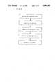
- FIG. 1is a flow chart showing the steps of a preferred embodiment of a method for mounting electronic parts in accordance with the present invention.
- FIG. 2(a), FIG. 2(b), FIG. 2(c) and FIG. 2(d)are side views showing the steps of the method for mounting electronic parts shown in FIG. 1.
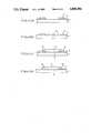
- FIG. 3is a flow chart showing steps of another preferred embodiment of a method for mounting electronic parts in accordance with the present invention.
- FIG. 4(a), FIG. 4(b), FIG. 4(c) and FIG. 4(d)are side views showing the steps of the method for mounting electronic parts shown in FIG. 3.
- FIG. 1One of the most preferred embodiments of a method for mounting electronic parts in accordance with the present invention is described as follows, with reference to FIG. 1, FIG. 2(a), FIG. 2(b), FIG. 2(c) and FIG. 2(d).
- An adhesive having capabilities of being photopolymerized and thermally polymerizedis made up by mixing and melting of alkylacrylate or trimethylolpropanetriacrylate, containing an acryloyl group as its photopolymerization functional group, 1-hydroxy cyclohexyl-phenylketone, which is an intensifying agent for ultraviolet rays, bisphenol A-type epoxy resin containing glycidyl group as a thermal polymerization functional group, tertiary amine as a curing agent for the epoxy resin and rosin as a viscosity-increasing sub-agent.
- Electronic partsare mounted by following the steps shown in FIG. 1 with the above-mentioned adhesive.
- the adhesive 3is applied at positions on a printed circuit substrate 1 on which the electronic parts are to be loaded by using a press-discharge type dispenser.
- ultraviolet raysare irradiated for ten seconds by means of a high-pressure mercury lamp for gelating the adhesive 3 so as to destroy the fluidity of the adhesive and to give pressure-sensitive adhesion ability to the adhesive.
- the printed circuit substrate 1 bearing such a pressure-sensitive adhesiveis set on an automatic parts-loading machine, and the chip-type electronic parts 4 are loaded one-by-one on selected positions where the adhesive 3 is already gelated, and adequately pressed by a mounting head for adhering the electronic parts on the substrate as shown in FIG. 2(b).
- the printed circuit substrate 1is vibrated or moved at high speed in a level plane, position errors of the chip-type electronic parts 4 may not occur.
- the printed circuit substrateis heated for three minutes at 150° C. for hardening the adhesive 3, and thereby the pressure-sensitive adhesion ability is destroyed.
- the printed circuit substrate 1is put upside-down in a jet flow solder tub as shown in FIG. 2(c) for spraying solder flow 5, and the soldering land 2 of the printed circuit substrate 1 and the electrode 6 of the electronic parts 4 are soldered by the solder 10 which is the congealed solder flow 5 as shown in FIG. 2(d).
- the heating process for hardening the adhesivecan be replaced with preliminary heating of the printed circuit substrate on which flux is applied before jet flow soldering or with heating of the solder flow.
- an adhesive which is subject to photopolymerization and thermal polymerizationis made up in the same way as in the above-described embodiment.
- the solder paste 7is applied on the soldering land 2 (which is a conductor part on which the soldering is made) of the printed circuit substrate 1 by a using screen printing method, as shown in FIG. 4(a).
- the solder pasteis a mixure of granular solder and dissolved rosin in an organic solvent.
- the adhesive 3is applied to selected positions on a printed circuit substrate 1 on which the electronic parts are to be loaded by using a press-discharge type dispenser as shown FIG. 4(b).
- ultraviolet raysare irradiated for ten seconds on the adhesive 3 for gelating the adhesive so as to destroy the fluidity thereof and to give pressure-sensitive adhesion ability thereto by using a high-pressure mercury lamp in which the infrared rays are reduced by a cold mirror (heat-absorbing filter) so as not to be over 60° C. higher than the temperature of the printed circuit substrate.
- a high-pressure mercury lampin which the infrared rays are reduced by a cold mirror (heat-absorbing filter) so as not to be over 60° C. higher than the temperature of the printed circuit substrate.
- a circuit substrate 1is set on an automatic parts-loading machine, and the chip-type electronic parts 4 are serially loaded on the gelated adhesive 3 and adequately pressed by a mounted head for adhering the parts on the substrate as shown in FIG. 4(b).
- soldering paste 7is melted by heating the printed circuit substrate 1 by heat radiation of a panel heater, or hot blast. And the soldering lands 2 of the printed circuit substrate 1 and the electrode 6 of the chip-type electronic parts 4 are soldered by solder 10 as shown in FIG. 4(d).
- the adhesive 3is hardened by heating in the solder reflow process at the same time.
- the heat-resisting ability of the adhesiveis improved and the pressure-sensitive adhesion ability is destroyed.
- the applying of a press-discharge-type adhesive dispenser or a screen printing-using stencilcan be applied.
- the adhesiveby a adhesive dispencer, it is desirable to make the discharging nozzle have a dispensing opening of rectangular or elliptic slit shape, to apply the adhesive 3 on the printed circuit substrate 1 in a film-like shape.
- the application of the adhesive 3is made by putting the dispensing opening of the discharging nozzle close to the printed circuit substrate and moving the nozzle, so as to move it in a direction perpendicular to the major axis of the nozzle opening.
- Such a methodcan prevent separation of the terminals of the electronic parts from the soldering land of the printed circuit substrate when the thickness of the adhesive is too large by being applied in a dot-like pattern.
- the application of the adhesive by screen printingmakes controlling of the thickness of the adhesive easy. But when the application of the adhesive and subsequent application of the soldering paste are made by a common screen printing method, there was a fear that the adhesive would be undesirably removed by touching of the stencil thereto in the application of the paste solder. Therefore, in order to overcome such trouble, it is preferable to provide grooves on positions where the stencil contacts with the adhesive during printing of the soldering paste.
Landscapes
- Engineering & Computer Science (AREA)
- Manufacturing & Machinery (AREA)
- Microelectronics & Electronic Packaging (AREA)
- Electric Connection Of Electric Components To Printed Circuits (AREA)
- Adhesives Or Adhesive Processes (AREA)
Abstract
Description
Claims (18)
Applications Claiming Priority (4)
| Application Number | Priority Date | Filing Date | Title |
|---|---|---|---|
| JP61216607AJPH0824213B2 (en) | 1986-09-12 | 1986-09-12 | Electronic component mounting method |
| JP61-216608 | 1986-09-12 | ||
| JP61216608AJP2589679B2 (en) | 1986-09-12 | 1986-09-12 | Electronic component mounting method |
| JP61-216607 | 1986-09-12 |
Publications (1)
| Publication Number | Publication Date |
|---|---|
| US4880486Atrue US4880486A (en) | 1989-11-14 |
Family
ID=26521534
Family Applications (1)
| Application Number | Title | Priority Date | Filing Date |
|---|---|---|---|
| US07/095,182Expired - LifetimeUS4880486A (en) | 1986-09-12 | 1987-09-11 | Method for mounting electronic parts |
Country Status (2)
| Country | Link |
|---|---|
| US (1) | US4880486A (en) |
| KR (1) | KR910000998B1 (en) |
Cited By (23)
| Publication number | Priority date | Publication date | Assignee | Title |
|---|---|---|---|---|
| US5137936A (en)* | 1989-07-26 | 1992-08-11 | Matsushita Electric Industrial Co., Ltd. | Method for packaging electronic parts and adhesive for use in said method |
| US5154791A (en)* | 1989-03-23 | 1992-10-13 | Thera Patent Gmbh & Co. Kg Gesellschaft Fur Industrielle | Method for bonding or potting substrates |
| US5296063A (en)* | 1990-03-20 | 1994-03-22 | Sharp Kabushiki Kaisha | Method for mounting a semiconductor device |
| US5318651A (en)* | 1991-11-27 | 1994-06-07 | Nec Corporation | Method of bonding circuit boards |
| US5354414A (en)* | 1988-10-05 | 1994-10-11 | Michael Feygin | Apparatus and method for forming an integral object from laminations |
| US5366573A (en)* | 1989-07-12 | 1994-11-22 | Siemens Nixdorf Informationssysteme Ag | UV-curable adhesive semiconductor chip mounting process |
| US5399220A (en)* | 1992-10-22 | 1995-03-21 | Optical Disc Corporation | Composite disc media and method for making same |
| US5529957A (en)* | 1995-04-06 | 1996-06-25 | Vlsi Technology, Inc. | Method for blocking contamination and stabilizing chip capacitor during attachment using a tape strip |
| US5558735A (en)* | 1991-12-27 | 1996-09-24 | Square D Company | Method for making laminate with U. V. cured polymer coating |
| WO1996032246A1 (en)* | 1995-04-14 | 1996-10-17 | Irvine Sensors Corporation | Dry adhesive joining of layers of electronic devices |
| US5575873A (en)* | 1991-08-06 | 1996-11-19 | Minnesota Mining And Manufacturing Company | Endless coated abrasive article |
| US5637175A (en)* | 1988-10-05 | 1997-06-10 | Helisys Corporation | Apparatus for forming an integral object from laminations |
| US5644837A (en)* | 1995-06-30 | 1997-07-08 | Lambda Technologies, Inc. | Process for assembling electronics using microwave irradiation |
| US5698059A (en)* | 1992-11-10 | 1997-12-16 | Alliedsignal Inc. | Filter and method for manufacturing filters |
| US5730817A (en)* | 1996-04-22 | 1998-03-24 | Helisys, Inc. | Laminated object manufacturing system |
| US5876550A (en)* | 1988-10-05 | 1999-03-02 | Helisys, Inc. | Laminated object manufacturing apparatus and method |
| US6206066B1 (en)* | 1995-12-15 | 2001-03-27 | Matsushita Electric Industrial Co., Ltd. | Apparatus for mounting an electronic component |
| US6497786B1 (en) | 1997-11-06 | 2002-12-24 | Nike, Inc. | Methods and apparatus for bonding deformable materials having low deformation temperatures |
| US6505665B1 (en)* | 1998-09-17 | 2003-01-14 | Intermedics, Inc. | Method and apparatus for use in assembling electronic devices |
| US20070261233A1 (en)* | 1994-04-26 | 2007-11-15 | Fujitsu Limited | Method and system for fabricating a semiconductor device |
| US9277787B2 (en) | 2013-03-15 | 2016-03-08 | Nike, Inc. | Microwave bonding of EVA and rubber items |
| US9781778B2 (en) | 2013-03-15 | 2017-10-03 | Nike, Inc. | Customized microwaving energy distribution utilizing slotted wave guides |
| US9955536B2 (en) | 2013-03-15 | 2018-04-24 | Nike, Inc. | Customized microwave energy distribution utilizing slotted cage |
Citations (4)
| Publication number | Priority date | Publication date | Assignee | Title |
|---|---|---|---|---|
| US4127432A (en)* | 1976-04-12 | 1978-11-28 | Matsushita Electric Industrial Co., Ltd. | Method for mounting chip type circuit elements on a printed circuit board and apparatus for performing the same |
| US4243500A (en)* | 1978-12-04 | 1981-01-06 | International Coatings, Co., Inc. | Pressure sensitive adhesives |
| US4372802A (en)* | 1980-06-02 | 1983-02-08 | Tokyo Denki Kagaku Kogyo Kabushiki Kaisha | Apparatus for mounting chip type circuit elements on printed circuit boards |
| US4720317A (en)* | 1985-02-14 | 1988-01-19 | Bando Chemical Industries, Ltd. | Method for dicing a semiconductor wafer |
- 1987
- 1987-09-10KRKR1019870010050Apatent/KR910000998B1/ennot_activeExpired
- 1987-09-11USUS07/095,182patent/US4880486A/ennot_activeExpired - Lifetime
Patent Citations (5)
| Publication number | Priority date | Publication date | Assignee | Title |
|---|---|---|---|---|
| US4127432A (en)* | 1976-04-12 | 1978-11-28 | Matsushita Electric Industrial Co., Ltd. | Method for mounting chip type circuit elements on a printed circuit board and apparatus for performing the same |
| US4243500A (en)* | 1978-12-04 | 1981-01-06 | International Coatings, Co., Inc. | Pressure sensitive adhesives |
| US4311759A (en)* | 1978-12-04 | 1982-01-19 | International Coatings Co., Inc. | Pressure sensitive adhesives |
| US4372802A (en)* | 1980-06-02 | 1983-02-08 | Tokyo Denki Kagaku Kogyo Kabushiki Kaisha | Apparatus for mounting chip type circuit elements on printed circuit boards |
| US4720317A (en)* | 1985-02-14 | 1988-01-19 | Bando Chemical Industries, Ltd. | Method for dicing a semiconductor wafer |
Cited By (27)
| Publication number | Priority date | Publication date | Assignee | Title |
|---|---|---|---|---|
| US5354414A (en)* | 1988-10-05 | 1994-10-11 | Michael Feygin | Apparatus and method for forming an integral object from laminations |
| US5876550A (en)* | 1988-10-05 | 1999-03-02 | Helisys, Inc. | Laminated object manufacturing apparatus and method |
| US5637175A (en)* | 1988-10-05 | 1997-06-10 | Helisys Corporation | Apparatus for forming an integral object from laminations |
| US5154791A (en)* | 1989-03-23 | 1992-10-13 | Thera Patent Gmbh & Co. Kg Gesellschaft Fur Industrielle | Method for bonding or potting substrates |
| US5366573A (en)* | 1989-07-12 | 1994-11-22 | Siemens Nixdorf Informationssysteme Ag | UV-curable adhesive semiconductor chip mounting process |
| US5137936A (en)* | 1989-07-26 | 1992-08-11 | Matsushita Electric Industrial Co., Ltd. | Method for packaging electronic parts and adhesive for use in said method |
| US5296063A (en)* | 1990-03-20 | 1994-03-22 | Sharp Kabushiki Kaisha | Method for mounting a semiconductor device |
| US5575873A (en)* | 1991-08-06 | 1996-11-19 | Minnesota Mining And Manufacturing Company | Endless coated abrasive article |
| US5318651A (en)* | 1991-11-27 | 1994-06-07 | Nec Corporation | Method of bonding circuit boards |
| US5558735A (en)* | 1991-12-27 | 1996-09-24 | Square D Company | Method for making laminate with U. V. cured polymer coating |
| US5399220A (en)* | 1992-10-22 | 1995-03-21 | Optical Disc Corporation | Composite disc media and method for making same |
| US5698059A (en)* | 1992-11-10 | 1997-12-16 | Alliedsignal Inc. | Filter and method for manufacturing filters |
| US20070281395A1 (en)* | 1994-04-26 | 2007-12-06 | Fujitsu Limited | Method and system for fabricating a semiconductor device |
| US20070261233A1 (en)* | 1994-04-26 | 2007-11-15 | Fujitsu Limited | Method and system for fabricating a semiconductor device |
| US5529957A (en)* | 1995-04-06 | 1996-06-25 | Vlsi Technology, Inc. | Method for blocking contamination and stabilizing chip capacitor during attachment using a tape strip |
| WO1996032246A1 (en)* | 1995-04-14 | 1996-10-17 | Irvine Sensors Corporation | Dry adhesive joining of layers of electronic devices |
| US5635010A (en)* | 1995-04-14 | 1997-06-03 | Pepe; Angel A. | Dry adhesive joining of layers of electronic devices |
| US5644837A (en)* | 1995-06-30 | 1997-07-08 | Lambda Technologies, Inc. | Process for assembling electronics using microwave irradiation |
| US6206066B1 (en)* | 1995-12-15 | 2001-03-27 | Matsushita Electric Industrial Co., Ltd. | Apparatus for mounting an electronic component |
| US6527905B1 (en) | 1995-12-15 | 2003-03-04 | Matsushita Electric Industrial Co., Ltd. | Method for mounting electronic components and apparatus and dispenser used in the method |
| US5730817A (en)* | 1996-04-22 | 1998-03-24 | Helisys, Inc. | Laminated object manufacturing system |
| US6497786B1 (en) | 1997-11-06 | 2002-12-24 | Nike, Inc. | Methods and apparatus for bonding deformable materials having low deformation temperatures |
| US6505665B1 (en)* | 1998-09-17 | 2003-01-14 | Intermedics, Inc. | Method and apparatus for use in assembling electronic devices |
| US9277787B2 (en) | 2013-03-15 | 2016-03-08 | Nike, Inc. | Microwave bonding of EVA and rubber items |
| US9781778B2 (en) | 2013-03-15 | 2017-10-03 | Nike, Inc. | Customized microwaving energy distribution utilizing slotted wave guides |
| US9955536B2 (en) | 2013-03-15 | 2018-04-24 | Nike, Inc. | Customized microwave energy distribution utilizing slotted cage |
| US10239260B2 (en) | 2013-03-15 | 2019-03-26 | Nike, Inc. | Microwave bonding of EVA and rubber items |
Also Published As
| Publication number | Publication date |
|---|---|
| KR880004730A (en) | 1988-06-07 |
| KR910000998B1 (en) | 1991-02-19 |
Similar Documents
| Publication | Publication Date | Title |
|---|---|---|
| US4880486A (en) | Method for mounting electronic parts | |
| US6909194B2 (en) | Electronic assembly having semiconductor component with polymer support member and method of fabrication | |
| US6180504B1 (en) | Method for fabricating a semiconductor component with external polymer support layer | |
| US6169022B1 (en) | Method of forming projection electrodes | |
| KR20010085224A (en) | Method for fixing a semiconductor device | |
| JPH11297886A (en) | Solder bump formation method | |
| US5871592A (en) | Solder and soldering method | |
| JP2014143316A (en) | Resin sealing method of flip chip component | |
| JP2000100862A (en) | Bare chip mounting method | |
| JPH11274209A (en) | Formation of bump electrode | |
| JP2589679B2 (en) | Electronic component mounting method | |
| JPS6345892A (en) | Method of mounting surface mount type electronic device | |
| CN112916972A (en) | Power chip tooling-free positioning welding method | |
| JP2000058597A (en) | Electronic component mounting method | |
| JPH0888248A (en) | Face-down bonding method and connecting material using thereof | |
| Gilleo et al. | The ultimate flip chip-integrated flux/underfill | |
| JP2000315855A (en) | Face-down mounting board and face-down mounting method | |
| JP2940252B2 (en) | Semiconductor device mounting structure and mounting method | |
| JP7656826B2 (en) | Mounting board and method for manufacturing the same | |
| JPS63151031A (en) | How to connect semiconductor devices | |
| JPS5811114B2 (en) | Mounting method of micro parts on printed circuit board | |
| JP2001044231A (en) | Method of forming solder bumps and wiring board, semiconductor element, semiconductor package and manufacture thereof | |
| JPH03252197A (en) | Solder printing method | |
| EP1286577B1 (en) | Method of fixing electronic part | |
| JPH0590742A (en) | Method for forming solder resist film |
Legal Events
| Date | Code | Title | Description |
|---|---|---|---|
| AS | Assignment | Owner name:MATSUSHITA ELECTRIC INDUSTRIAL CO., LTD., 1006, OA Free format text:ASSIGNMENT OF ASSIGNORS INTEREST.;ASSIGNOR:MAEDA, YUKIO;REEL/FRAME:004843/0134 Effective date:19871002 Owner name:MATSUSHITA ELECTRIC INDUSTRIAL CO., LTD.,JAPAN Free format text:ASSIGNMENT OF ASSIGNORS INTEREST;ASSIGNOR:MAEDA, YUKIO;REEL/FRAME:004843/0134 Effective date:19871002 | |
| STCF | Information on status: patent grant | Free format text:PATENTED CASE | |
| FEPP | Fee payment procedure | Free format text:PAYOR NUMBER ASSIGNED (ORIGINAL EVENT CODE: ASPN); ENTITY STATUS OF PATENT OWNER: LARGE ENTITY | |
| FPAY | Fee payment | Year of fee payment:4 | |
| FEPP | Fee payment procedure | Free format text:PAYOR NUMBER ASSIGNED (ORIGINAL EVENT CODE: ASPN); ENTITY STATUS OF PATENT OWNER: LARGE ENTITY Free format text:PAYER NUMBER DE-ASSIGNED (ORIGINAL EVENT CODE: RMPN); ENTITY STATUS OF PATENT OWNER: LARGE ENTITY | |
| FPAY | Fee payment | Year of fee payment:8 | |
| FPAY | Fee payment | Year of fee payment:12 |