US4876430A - Preweld test method - Google Patents
Preweld test methodDownload PDFInfo
- Publication number
- US4876430A US4876430AUS07/223,497US22349788AUS4876430AUS 4876430 AUS4876430 AUS 4876430AUS 22349788 AUS22349788 AUS 22349788AUS 4876430 AUS4876430 AUS 4876430A
- Authority
- US
- United States
- Prior art keywords
- electrode
- electrodes
- sheets
- voltage
- applying
- Prior art date
- Legal status (The legal status is an assumption and is not a legal conclusion. Google has not performed a legal analysis and makes no representation as to the accuracy of the status listed.)
- Expired - Fee Related
Links
Images

Classifications
- B—PERFORMING OPERATIONS; TRANSPORTING
- B23—MACHINE TOOLS; METAL-WORKING NOT OTHERWISE PROVIDED FOR
- B23K—SOLDERING OR UNSOLDERING; WELDING; CLADDING OR PLATING BY SOLDERING OR WELDING; CUTTING BY APPLYING HEAT LOCALLY, e.g. FLAME CUTTING; WORKING BY LASER BEAM
- B23K11/00—Resistance welding; Severing by resistance heating
- B23K11/24—Electric supply or control circuits therefor
- B23K11/25—Monitoring devices
- B23K11/252—Monitoring devices using digital means
- B23K11/256—Monitoring devices using digital means the measured parameter being the inter-electrode electrical resistance
- Y—GENERAL TAGGING OF NEW TECHNOLOGICAL DEVELOPMENTS; GENERAL TAGGING OF CROSS-SECTIONAL TECHNOLOGIES SPANNING OVER SEVERAL SECTIONS OF THE IPC; TECHNICAL SUBJECTS COVERED BY FORMER USPC CROSS-REFERENCE ART COLLECTIONS [XRACs] AND DIGESTS
- Y10—TECHNICAL SUBJECTS COVERED BY FORMER USPC
- Y10S—TECHNICAL SUBJECTS COVERED BY FORMER USPC CROSS-REFERENCE ART COLLECTIONS [XRACs] AND DIGESTS
- Y10S136/00—Batteries: thermoelectric and photoelectric
- Y10S136/29—Testing, calibrating, treating, e.g. aging
Definitions
- This inventionrelates to methods for joining two conductive sheets by welding.
- One method of welding together two sheets of electrically conductive materialis to juxtapose the sheets by placing one sheet over the other in the region to be welded, and then sandwiching the sheets between a pair of welding electrodes. A high current is then passed through the electrodes, through the sheets of metal and their interface to thereby heat the metal near the interface to a fusion or welding temperature.
- Other methodsmay be used for semiconductor welding, as for example, rapidly vibrating one of the pieces to be joined against the other, to thereby generate fusing heat at the moving interface and to concurrently scrape the area clear of oxides and dirt.
- Japanese Patent Document No. 56-160885describes a system for welding semiconductor elements on a substrate including a pair of welding electrodes and means for metering optimum contact resistance between the electrodes and the parts to be welded prior to welding, for achieving optimum contact resistance between the electrodes and the part despite the existence of oxidized films or other foreign material on the parts.
- a high reliability methodis desired for welding together two sheets of conductive material accessible for welding from only one side.
- a method for welding together two sheets of electrically conductive materialincludes the step of placing a first side of a first sheet of the electrically conductive material in contact with a first side of a second sheet of electrically conductive material at least in a region to be welded.
- First and second welding electrodesare applied to a second side of the first sheet of material straddling the region to be welded.
- a third electrodeis applied to the second sheet of electrically conductive material adjacent the region to be welded.
- the electrical resistance between at least one of the first and second electrodes and the third electrodeis measured and compared with a predetermined value of electrical resistance. If the measured electrical resistance is below the predetermined value, welding energy is applied between the first and second electrodes to cause fusion between the first and second sheets in the region to be welded. If the measured resistance exceeds the predetermined value, at least a portion of the first side of a sheet in the region to be welded is cleaned.
- the third electrodeis applied to the first side of the second sheet.
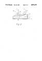
- FIG. 1ais a perspective or isometric view of a welding arrangement and a workpiece according to the invention, together with a block diagram of a welding arrangement in accordance with the invention
- FIG. 1bis a cross-section of a portion of the arrangement of FIG. 1a and FIGS. 1a and 1b are together referred to as FIG. 1;
- FIG. 2is a representation of an elevation cross-section of the workpiece FIG. 1 with welding electrodes in place, illustrating the flow of welding current
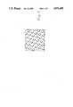
- FIG. 3is a tracing of a photomicrograph of a portion of the workpiece illustrated in FIG. 1.
- FIG. 1provides improved reliability.
- a plurality of individual solar cells 10a, 10b, 10c . . . 10fare illustrated as rectangles which are spaced apart to more clearly illustrate their separate nature, but which may be contiguous or closely juxtaposed to maximize the amount of surface coverage and to thereby minimize the length of interconnections.
- Each individual solar cell 10includes a bottom metallization 12.
- solar cell 10aincludes a bottom metallization 12a
- solar cell 10cincludes a bottom metallization 12c
- Bottom metallizations 12 of the solar cellsare interconnected in the final array by a welding method according to the invention, which is not described in detail but which will be obvious from the description herein.
- the bottom metallizationsinclude a relatively wide portion adjacent a long edge and strips extending across the bottom of the solar cell which leave large portions non-metallized for penetration by photons of light.
- Each individual solar cell 10also includes an upper metallization contact 14 which essentially covers the top surface.
- solar cell 10ahas disposed upon its upper surface a metallization surface 14a
- solar cell 10bhas a metallization surface 14b, etc.
- the disposition of the upper and lower metallization surfaces of solar cell 10cis more clearly visible in the cross-section of FIG. 1b, taken at section lines 1b--1b of FIG. 1a.
- each solar cell 10is connected to the wide portion of the bottom metallization 12 of the next adjacent solar cell on one side by means of a conductive connection strip 16.
- upper metallization 14b of solar cell 10bis connected by strip 16b to bottom metallization 12c of solar cell 10c
- upper metallization 14c of solar cell 10cis connected by strip 16c to bottom metallization 12d of solar cell 10d.
- Each conductive strip 16is welded to each of the associated metallizations of the solar cells to interconnect the contacts to form a series circuit.
- Electrodes 20, 22, and 24are desirably made from copper for high conductivity and are tipped with molybdenum (Mb), which has a high melting temperature, for low wear. Electrodes 20, 22, and 24 are held in a mutually spaced relationship by a holder (not illustrated) which is capable of up and down motion relative to the upper surface of the solar cells, as illustrated by two-headed arrow 26. Electrodes 20, 22 and 24 are electrically isolated from each other when not in contact with a conductive strip 16. Electrodes 20, 22, and 24 are connected by conductors of suitable size to a switch arrangement illustrated as a block 30. Switch arrangement 30 receives control signals over a conductor set 32 and electrical power over a conductor set 34 for applying voltage or current to pairs of electrodes 20, 22, and 24 under the command of a control circuit illustrated as a block 38.
- Mbmolybdenum
- electrode set 20, 22 and 24is moved relative to the array of solar cells by either stepping the solar cell array under the set of electrodes or by moving the set of electrodes along the array.
- each conductive strip 16defines an aperture 18 along one edge thereof.
- the aperture sizeis much smaller than the surface of the solar cell, and are located so that at least one aperture 18 overlies each metallization 14 of solar cell 10.
- Welded regions 19a and 19bconnect a strip 16 to upper metallization contact 14a and 14b of solar cells 10a and 10b, respectively.
- electrode set 20, 22, 24is above solar cell 10c, in readiness for commencement of a welding operation in accordance with the invention.
- Electrodes 20 and 22are lowered into contact with conductive strip 16c.
- Switch 40is closed by an operator to initiate the welding procedure.
- Switch 40is connected to a control circuit illustrated as a block 38.
- the welding procedurebegins with control block 38 setting a controllable current source 36 to produce a relatively low voltage, and also setting switch 30 to a position in which controllable current source 36 applies the voltage between electrodes 20 and 22 to cause a relatively low current, such as one ampere, to flow.
- the switches of block 30have zero resistance, and consequently measurements of electrode voltage may be made at controllable current source 36.
- measurements of electrode voltagemay be made on the electrode side of switch block 30 if the switch or other circuit resistances are significant. Signals representing the measured voltage and the resulting current are coupled from controllable current source 36 to control block 38. The ratio of the voltage applied across electrodes 20 and 22 to the resulting current is calculated to determine the resistance.
- source 36may be set to produce a known current, and the resistance may be determined from the resulting voltage.
- the resistance through the circuit including electrodes 20 and 22is compared with a predetermined standard resistance.
- the resistance in this circuitincludes the resistances of the two electrodes 20 and 22, the resistance at the contact interface between each electrode 20, 22 and connector strip 16c, and the resistance of strip 16c in the gap between electrodes 20 and 22. Since connector strip 16 is in contact with the surface of metallization 14c of solar cell 10c, the resistance of connector strip 16 is influenced by the resistance of metallization 14c and by the contact resistance between connector strip 16 and metallization 14c.
- the resistances of electrodes 20 and 22, and the resistance of strip 16, whether or not paralleled by metallization 14care cumulatively relatively small by comparison with the contact resistance between an electrode 20, 22 and connector strip 16 when the tip of the electrode is dirty or eroded.
- the predetermined resistance value with which the measured value of resistance is comparedcan be set well above the sum of the resistances of the two electrodes and of the contact strip so that clean, uneroded electrodes tips will seldom exceed the threshold, but dirty or eroded tips will almost always cause the threshold to be exceeded.
- control block 38ceases the welding process and illuminates a warning lamp illustrated as 41 to indicate to the operator that the tips of the welding electrodes 20, 22 should be cleaned.
- the cleaning operationsare standard and not a part of the invention.
- control block 38operates switch 30 to disconnect one of electrodes 20, 22 from the circuit and to connect the output voltage of controllable source 36 across electrode 24 and the remaining one of electrodes 20 and 22. Concurrently with operation of switch 30, control block 38 sets controllable current source 36 to a low voltage condition.
- a voltage applied to electrode 24 relative to (for example) electrode 20causes current to flow through electrodes 20 and 24, vertically through connection strip 16c, through the point or points of contact between connection strip 16 and metallization 14c, laterally through metallization 14c to a point under electrode 24 and through the point of contact between electrode 24 and metallization 14c.
- the resistances of electrodes 20 and 24are relatively small, and the resistance at the interface between electrode 24 and metallization 14c is also relatively small because of the large pressure per unit area attributable to the small tip diameter of electrode 24.
- the previous resistance measurementalso established that the contact resistance between electrode 20 and connection strip 16c is relatively low.
- One remaining unknown resistanceis the contact resistance between connection strip 16c and metallization 14c. This resistance can be increased by the presence of dirt or oxides at the interface. Such dirt or oxides are in the region in which fusion will take place during welding, and may adversely affect the reliability of the resulting weld.
- Control block 38responds to the comparison between the measured resistance the threshold to either proceed with the next step in the welding operation if the resistance is low, or if high to interrupt the welding procedure and illuminate a lamp illustrated as 43 to indicate to the operator that the welding procedure has been interrupted and that the interface between connection strip 16c and metallization 14c requires cleaning.
- control block 38proceeds by disconnecting electrode 24 from the circuit and reconnecting electrodes 20 and 22 across the output of controllable source 36. Concurrently, control block 38 also sets controllable current source 36 to the welding conditions (high voltage or current) and energizes the source to apply voltage across or current through electrodes 20 and 22 to effectuate the weld.
- FIG. 2is a cross section of the structure of FIG. 1a with welding electrodes 20, 22 in contact with the upper side of connection strip 16.
- welding electrode 22is made relatively positive (+) and electrode 20 relatively negative (-).
- Conventional currentflows in the direction illustrated by the arrows, a portion illustrated as 210 flowing laterally through connection strip 16 between the electrodes, and another portion 212 flowing through metallization 14.
- the magnitude of the current portions 210, 212is selected to be large enough so that the energy per unit time (power) dissipated in the internal resistance of the conductors raises the material to fusion temperature, thereby causing a fusion or welding of the connection strip 16 to metallization 14 at a location between the welding electrodes.
- Control block 38then turns off source 36 and raises the electrodes preparatory for the next command to again perform the welding routine. It may also reposition the solar cell array under the welding electrodes in readiness for welding cell 10d.
- the programming of control block 38 to perform the described routineis believed to be well within ordinary skill in the art and is not described in detail. The method as described provides consistent welds because welds are not made through dirty or corroded interfaces.
- connection strip 16is desirably made from an expanded metal mesh or from an etched mesh.
- FIG. 3illustrates a tracing of a photomicrograph of a portion of an etched mesh having diamond-shaped perforations. It has been found that if the tips of welding electrodes 20 and 22 are pointed, the point when lowered may land on a single interconnection connection strip of the mesh. When the high welding current is applied, this may undesirably result in melting of the strip which happens to be directly underneath the welding electrode. This is avoided by welding electrodes shaped as illustrated in FIG. 1, having the form of a blade which makes contact with more than one connection strip of the mesh, which thereby eliminates the problem.
- the up-and-down motion of electrode 24may be independent of the motion of electrodes 20 and 22, and electrode 24 may be lowered into contact with the associated metallization only when connections are made thereto by switch 30.
- switch 30may connect electrodes 20 and 22 in common, to reduce the effect of contact resistance.
- a further stepmay be added, measuring the sheet interface resistance by the use of two slightly different paths, first between electrodes 20 and 24 and then between electrodes 22 and 24. If conductive strip 16 is a woven mesh, discrete apertures 18 may not be required if electrode 24 is insulated along its length, as electrode 24 can penetrate the mesh by pushing aside mesh wires.
- the welding currentmay be alternating (AC) or direct (DC), and may be controlled in amplitude and/or duration. While indicator lamps have been described, buzzers, liquid crystal displays, or any other type of annunciator or display may be used. An inert gas may be used to prevent oxidation during welding.
Landscapes
- Engineering & Computer Science (AREA)
- Mechanical Engineering (AREA)
- Resistance Welding (AREA)
- Wire Bonding (AREA)
Abstract
Description
Claims (16)
Priority Applications (3)
| Application Number | Priority Date | Filing Date | Title |
|---|---|---|---|
| US07/223,497US4876430A (en) | 1988-07-25 | 1988-07-25 | Preweld test method |
| DE3923433ADE3923433A1 (en) | 1988-07-25 | 1989-07-15 | METHOD FOR WELDING SHEETS |
| JP1184876AJPH0270388A (en) | 1988-07-25 | 1989-07-19 | Method of testing article before welding |
Applications Claiming Priority (1)
| Application Number | Priority Date | Filing Date | Title |
|---|---|---|---|
| US07/223,497US4876430A (en) | 1988-07-25 | 1988-07-25 | Preweld test method |
Publications (1)
| Publication Number | Publication Date |
|---|---|
| US4876430Atrue US4876430A (en) | 1989-10-24 |
Family
ID=22836771
Family Applications (1)
| Application Number | Title | Priority Date | Filing Date |
|---|---|---|---|
| US07/223,497Expired - Fee RelatedUS4876430A (en) | 1988-07-25 | 1988-07-25 | Preweld test method |
Country Status (3)
| Country | Link |
|---|---|
| US (1) | US4876430A (en) |
| JP (1) | JPH0270388A (en) |
| DE (1) | DE3923433A1 (en) |
Cited By (26)
| Publication number | Priority date | Publication date | Assignee | Title |
|---|---|---|---|---|
| US5064987A (en)* | 1990-08-24 | 1991-11-12 | Crafford Precision Products Co. | Resistance welding apparatus with power control for reduced arcing |
| EP0491578A1 (en)* | 1990-12-19 | 1992-06-24 | Sollac | Resistance spot welding method and welding electrode to carry out the method |
| US5272306A (en)* | 1991-10-01 | 1993-12-21 | Akio Hirane | Spot welding apparatus and method |
| US5308948A (en)* | 1992-01-28 | 1994-05-03 | Nippondenso Co., Ltd. | Method for welding together electrically conductive members |
| US5418347A (en)* | 1993-05-19 | 1995-05-23 | Odawara Automation Inc. | Method and apparatus for fusing terminal or commutator wire connections using a trigger current |
| WO1999008825A1 (en)* | 1997-08-14 | 1999-02-25 | Magna Ihv Gesellschaft Für Innenhochdruckverfahren Mbh | Assembling electroconductive parts by electric current heating |
| US6459064B1 (en) | 1997-08-14 | 2002-10-01 | Magna IHV Gesellschaft fur Innenhochdruck—Verfahren mbH | Assembling electroconductive parts by electric current heating |
| US20030038368A1 (en)* | 2001-07-31 | 2003-02-27 | Hiroshi Maeda | Production apparatus of planer type semiconductor device and fabrication method of planer type semiconductor device |
| US20070089573A1 (en)* | 2005-10-24 | 2007-04-26 | Lectro Engineering Company | Spin trimmer and method of trimming |
| US7898053B2 (en)* | 2000-02-04 | 2011-03-01 | Daniel Luch | Substrate structures for integrated series connected photovoltaic arrays and process of manufacture of such arrays |
| US7989692B2 (en) | 1999-03-30 | 2011-08-02 | Daniel Luch | Substrate and collector grid structures for integrated series connected photovoltaic arrays and process of manufacturing of such arrays |
| US8076568B2 (en) | 2006-04-13 | 2011-12-13 | Daniel Luch | Collector grid and interconnect structures for photovoltaic arrays and modules |
| US8110737B2 (en) | 1999-03-30 | 2012-02-07 | Daniel Luch | Collector grid, electrode structures and interrconnect structures for photovoltaic arrays and methods of manufacture |
| US8138413B2 (en) | 2006-04-13 | 2012-03-20 | Daniel Luch | Collector grid and interconnect structures for photovoltaic arrays and modules |
| US20120074113A1 (en)* | 2010-09-29 | 2012-03-29 | Honda Motor Co., Ltd. | Spot welding method and spot welding apparatus |
| US8198696B2 (en) | 2000-02-04 | 2012-06-12 | Daniel Luch | Substrate structures for integrated series connected photovoltaic arrays and process of manufacture of such arrays |
| US8222513B2 (en) | 2006-04-13 | 2012-07-17 | Daniel Luch | Collector grid, electrode structures and interconnect structures for photovoltaic arrays and methods of manufacture |
| US8664030B2 (en) | 1999-03-30 | 2014-03-04 | Daniel Luch | Collector grid and interconnect structures for photovoltaic arrays and modules |
| US8729385B2 (en) | 2006-04-13 | 2014-05-20 | Daniel Luch | Collector grid and interconnect structures for photovoltaic arrays and modules |
| US8822810B2 (en) | 2006-04-13 | 2014-09-02 | Daniel Luch | Collector grid and interconnect structures for photovoltaic arrays and modules |
| CN104043896A (en)* | 2013-03-13 | 2014-09-17 | 本田技研工业株式会社 | Method for single-sided resistance welding |
| US8884155B2 (en) | 2006-04-13 | 2014-11-11 | Daniel Luch | Collector grid and interconnect structures for photovoltaic arrays and modules |
| US9006563B2 (en) | 2006-04-13 | 2015-04-14 | Solannex, Inc. | Collector grid and interconnect structures for photovoltaic arrays and modules |
| US9236512B2 (en) | 2006-04-13 | 2016-01-12 | Daniel Luch | Collector grid and interconnect structures for photovoltaic arrays and modules |
| US9865758B2 (en) | 2006-04-13 | 2018-01-09 | Daniel Luch | Collector grid and interconnect structures for photovoltaic arrays and modules |
| CN112317558A (en)* | 2020-09-04 | 2021-02-05 | 中国第一汽车股份有限公司 | Rapid electrical detection system and method for sheet number of stamping automatic line |
Families Citing this family (2)
| Publication number | Priority date | Publication date | Assignee | Title |
|---|---|---|---|---|
| EP2376255A1 (en) | 2008-12-12 | 2011-10-19 | Erdogan Karakas | Resistance welding method and device |
| JP4875718B2 (en)* | 2009-01-21 | 2012-02-15 | 株式会社井上製作所 | Flexible conductor and method for producing flexible conductor |
Citations (10)
| Publication number | Priority date | Publication date | Assignee | Title |
|---|---|---|---|---|
| US3462577A (en)* | 1966-12-23 | 1969-08-19 | Texas Instruments Inc | Welding method and apparatus |
| US3590372A (en)* | 1968-12-26 | 1971-06-29 | Ibm | Spreading resistance method and apparatus for determining the resistivity of a material |
| US3735254A (en)* | 1970-06-06 | 1973-05-22 | Philips Corp | Method of determining the sheet resistance and measuring device therefor |
| US3837924A (en)* | 1971-06-01 | 1974-09-24 | Trw Inc | Solar array |
| US3849880A (en)* | 1969-12-12 | 1974-11-26 | Communications Satellite Corp | Solar cell array |
| US4176313A (en)* | 1978-02-24 | 1979-11-27 | Teradyne, Inc. | Analyzing electrical circuit boards |
| US4178543A (en)* | 1978-02-23 | 1979-12-11 | Teradyne, Inc. | Analyzing electrical circuit boards |
| US4179652A (en)* | 1978-02-21 | 1979-12-18 | Teradyne, Inc. | Analyzing electrical circuit boards |
| US4218650A (en)* | 1978-06-23 | 1980-08-19 | Nasa | Apparatus for measuring semiconductor device resistance |
| JPS56160885A (en)* | 1980-05-14 | 1981-12-10 | Nippon Abionikusu Kk | Resistance welding equipment |
- 1988
- 1988-07-25USUS07/223,497patent/US4876430A/ennot_activeExpired - Fee Related
- 1989
- 1989-07-15DEDE3923433Apatent/DE3923433A1/ennot_activeWithdrawn
- 1989-07-19JPJP1184876Apatent/JPH0270388A/enactivePending
Patent Citations (10)
| Publication number | Priority date | Publication date | Assignee | Title |
|---|---|---|---|---|
| US3462577A (en)* | 1966-12-23 | 1969-08-19 | Texas Instruments Inc | Welding method and apparatus |
| US3590372A (en)* | 1968-12-26 | 1971-06-29 | Ibm | Spreading resistance method and apparatus for determining the resistivity of a material |
| US3849880A (en)* | 1969-12-12 | 1974-11-26 | Communications Satellite Corp | Solar cell array |
| US3735254A (en)* | 1970-06-06 | 1973-05-22 | Philips Corp | Method of determining the sheet resistance and measuring device therefor |
| US3837924A (en)* | 1971-06-01 | 1974-09-24 | Trw Inc | Solar array |
| US4179652A (en)* | 1978-02-21 | 1979-12-18 | Teradyne, Inc. | Analyzing electrical circuit boards |
| US4178543A (en)* | 1978-02-23 | 1979-12-11 | Teradyne, Inc. | Analyzing electrical circuit boards |
| US4176313A (en)* | 1978-02-24 | 1979-11-27 | Teradyne, Inc. | Analyzing electrical circuit boards |
| US4218650A (en)* | 1978-06-23 | 1980-08-19 | Nasa | Apparatus for measuring semiconductor device resistance |
| JPS56160885A (en)* | 1980-05-14 | 1981-12-10 | Nippon Abionikusu Kk | Resistance welding equipment |
Cited By (36)
| Publication number | Priority date | Publication date | Assignee | Title |
|---|---|---|---|---|
| US5064987A (en)* | 1990-08-24 | 1991-11-12 | Crafford Precision Products Co. | Resistance welding apparatus with power control for reduced arcing |
| EP0491578A1 (en)* | 1990-12-19 | 1992-06-24 | Sollac | Resistance spot welding method and welding electrode to carry out the method |
| FR2670698A1 (en)* | 1990-12-19 | 1992-06-26 | Lorraine Laminage | POINT RESISTANCE WELDING METHOD AND WELDING ELECTRODE FOR IMPLEMENTING THE METHOD. |
| US5229568A (en)* | 1990-12-19 | 1993-07-20 | Sollac | Spot resistance welding method and welding electrode for implementing the method |
| US5272306A (en)* | 1991-10-01 | 1993-12-21 | Akio Hirane | Spot welding apparatus and method |
| US5308948A (en)* | 1992-01-28 | 1994-05-03 | Nippondenso Co., Ltd. | Method for welding together electrically conductive members |
| US5418347A (en)* | 1993-05-19 | 1995-05-23 | Odawara Automation Inc. | Method and apparatus for fusing terminal or commutator wire connections using a trigger current |
| US6459064B1 (en) | 1997-08-14 | 2002-10-01 | Magna IHV Gesellschaft fur Innenhochdruck—Verfahren mbH | Assembling electroconductive parts by electric current heating |
| WO1999008825A1 (en)* | 1997-08-14 | 1999-02-25 | Magna Ihv Gesellschaft Für Innenhochdruckverfahren Mbh | Assembling electroconductive parts by electric current heating |
| US7989692B2 (en) | 1999-03-30 | 2011-08-02 | Daniel Luch | Substrate and collector grid structures for integrated series connected photovoltaic arrays and process of manufacturing of such arrays |
| US7989693B2 (en) | 1999-03-30 | 2011-08-02 | Daniel Luch | Substrate and collector grid structures for integrated series connected photovoltaic arrays and process of manufacture of such arrays |
| US8110737B2 (en) | 1999-03-30 | 2012-02-07 | Daniel Luch | Collector grid, electrode structures and interrconnect structures for photovoltaic arrays and methods of manufacture |
| US8664030B2 (en) | 1999-03-30 | 2014-03-04 | Daniel Luch | Collector grid and interconnect structures for photovoltaic arrays and modules |
| US8304646B2 (en) | 1999-03-30 | 2012-11-06 | Daniel Luch | Substrate and collector grid structures for integrated series connected photovoltaic arrays and process of manufacture of such arrays |
| US8198696B2 (en) | 2000-02-04 | 2012-06-12 | Daniel Luch | Substrate structures for integrated series connected photovoltaic arrays and process of manufacture of such arrays |
| US7898053B2 (en)* | 2000-02-04 | 2011-03-01 | Daniel Luch | Substrate structures for integrated series connected photovoltaic arrays and process of manufacture of such arrays |
| US20030038368A1 (en)* | 2001-07-31 | 2003-02-27 | Hiroshi Maeda | Production apparatus of planer type semiconductor device and fabrication method of planer type semiconductor device |
| US6797910B2 (en)* | 2001-07-31 | 2004-09-28 | Sharp Kabushiki Kaisha | Production apparatus of planer type semiconductor device and fabrication method of planer type semiconductor device |
| US20070089573A1 (en)* | 2005-10-24 | 2007-04-26 | Lectro Engineering Company | Spin trimmer and method of trimming |
| US8884155B2 (en) | 2006-04-13 | 2014-11-11 | Daniel Luch | Collector grid and interconnect structures for photovoltaic arrays and modules |
| US9006563B2 (en) | 2006-04-13 | 2015-04-14 | Solannex, Inc. | Collector grid and interconnect structures for photovoltaic arrays and modules |
| US9865758B2 (en) | 2006-04-13 | 2018-01-09 | Daniel Luch | Collector grid and interconnect structures for photovoltaic arrays and modules |
| US8138413B2 (en) | 2006-04-13 | 2012-03-20 | Daniel Luch | Collector grid and interconnect structures for photovoltaic arrays and modules |
| US8729385B2 (en) | 2006-04-13 | 2014-05-20 | Daniel Luch | Collector grid and interconnect structures for photovoltaic arrays and modules |
| US8822810B2 (en) | 2006-04-13 | 2014-09-02 | Daniel Luch | Collector grid and interconnect structures for photovoltaic arrays and modules |
| US9236512B2 (en) | 2006-04-13 | 2016-01-12 | Daniel Luch | Collector grid and interconnect structures for photovoltaic arrays and modules |
| US8222513B2 (en) | 2006-04-13 | 2012-07-17 | Daniel Luch | Collector grid, electrode structures and interconnect structures for photovoltaic arrays and methods of manufacture |
| US8076568B2 (en) | 2006-04-13 | 2011-12-13 | Daniel Luch | Collector grid and interconnect structures for photovoltaic arrays and modules |
| US9505078B2 (en)* | 2010-09-29 | 2016-11-29 | Honda Motor Co., Ltd. | Spot welding method and spot welding apparatus |
| US20120074113A1 (en)* | 2010-09-29 | 2012-03-29 | Honda Motor Co., Ltd. | Spot welding method and spot welding apparatus |
| JP2014176897A (en)* | 2013-03-13 | 2014-09-25 | Honda Motor Co Ltd | Single-sided resistance welding method |
| CN104043896A (en)* | 2013-03-13 | 2014-09-17 | 本田技研工业株式会社 | Method for single-sided resistance welding |
| CN104043896B (en)* | 2013-03-13 | 2016-08-24 | 本田技研工业株式会社 | Method for one-sided resistance weldering |
| US9815136B2 (en) | 2013-03-13 | 2017-11-14 | Honda Motor Co., Ltd. | Method for single-sided resistance welding |
| CN112317558A (en)* | 2020-09-04 | 2021-02-05 | 中国第一汽车股份有限公司 | Rapid electrical detection system and method for sheet number of stamping automatic line |
| CN112317558B (en)* | 2020-09-04 | 2023-01-17 | 中国第一汽车股份有限公司 | Rapid electrical detection system and method for sheet number of stamping automatic line |
Also Published As
| Publication number | Publication date |
|---|---|
| DE3923433A1 (en) | 1990-02-01 |
| JPH0270388A (en) | 1990-03-09 |
Similar Documents
| Publication | Publication Date | Title |
|---|---|---|
| US4876430A (en) | Preweld test method | |
| US7339114B2 (en) | Cable, cable connection method and cable welder | |
| JP2562410B2 (en) | Electric resistance manufacturing method and electric resistance | |
| EP1267429B1 (en) | Battery cell and production method therefor | |
| US5193732A (en) | Apparatus and methods for making simultaneous electrical connections | |
| US3155809A (en) | Means and techniques for making electrical connections | |
| US5593604A (en) | Method of resistance welding thin elements | |
| US3252203A (en) | Welding process | |
| KR100218198B1 (en) | Method of connecting wire to terminal and apparatus therefor | |
| US3944777A (en) | Method for joining resistive and conductive materials | |
| US3523173A (en) | Insulated lead connection | |
| EP0243638B1 (en) | Microweld apparatus with an improved electrode tip design | |
| US5126527A (en) | High temperature solder device for flat cables | |
| US3374530A (en) | Process for the joinder of metallic members | |
| US3519778A (en) | Method and apparatus for joining electrical conductors | |
| JPS62289379A (en) | Method and device for joining covered wire | |
| CA1054725A (en) | Discontinuous semiconductor contact layers | |
| KR980012734A (en) | Method for electrically connecting the contact member of the plug connector to the connecting line | |
| JPH0249190B2 (en) | ||
| US3701877A (en) | Method and apparatus for making electrical connections | |
| JPS6230507B2 (en) | ||
| JP3003902B2 (en) | Dissimilar metal terminal welding method | |
| JP2564202B2 (en) | Spot Welding Electrode Testing Machine | |
| EP0064011A2 (en) | Electrode assembly system and process for automatic wire welding | |
| CN108364878B (en) | Micro- assemble method and chip apparatus |
Legal Events
| Date | Code | Title | Description |
|---|---|---|---|
| AS | Assignment | Owner name:GENERAL ELECTRIC COMPANY, NEW YORK, A CORP. OF NEW Free format text:ASSIGNMENT OF ASSIGNORS INTEREST.;ASSIGNORS:HERSCHITZ, ROMAN;BOGORAD, ALEXANDER;HARHIGH, ROBERT N.;REEL/FRAME:004924/0576 Effective date:19880719 Owner name:GENERAL ELECTRIC COMPANY, A CORP. OF NEW YORK, NEW Free format text:ASSIGNMENT OF ASSIGNORS INTEREST;ASSIGNORS:HERSCHITZ, ROMAN;BOGORAD, ALEXANDER;HARHIGH, ROBERT N.;REEL/FRAME:004924/0576 Effective date:19880719 | |
| AS | Assignment | Owner name:AMERICAN TREE COMPANY, INC., A CORP. OF KY, KENTUC Free format text:ASSIGNMENT OF ASSIGNORS INTEREST.;ASSIGNOR:AMERICAN TECHNICAL INDUSTRIES, INC.;REEL/FRAME:005268/0610 Effective date:19900208 | |
| FEPP | Fee payment procedure | Free format text:PAYOR NUMBER ASSIGNED (ORIGINAL EVENT CODE: ASPN); ENTITY STATUS OF PATENT OWNER: LARGE ENTITY | |
| FPAY | Fee payment | Year of fee payment:4 | |
| AS | Assignment | Owner name:MARTIN MARIETTA CORPORATION, MARYLAND Free format text:ASSIGNMENT OF ASSIGNORS INTEREST;ASSIGNOR:GENERAL ELECTRIC COMPANY;REEL/FRAME:007046/0736 Effective date:19940322 | |
| REMI | Maintenance fee reminder mailed | ||
| AS | Assignment | Owner name:LOCKHEED MARTIN CORPORATION, MARYLAND Free format text:ASSIGNMENT OF ASSIGNORS INTEREST;ASSIGNOR:MARTIN MARIETTA CORPORATION;REEL/FRAME:008628/0518 Effective date:19960128 | |
| LAPS | Lapse for failure to pay maintenance fees | ||
| FP | Lapsed due to failure to pay maintenance fee | Effective date:19971029 | |
| STCH | Information on status: patent discontinuation | Free format text:PATENT EXPIRED DUE TO NONPAYMENT OF MAINTENANCE FEES UNDER 37 CFR 1.362 |