US4876112A - Process for forming metallic patterned film - Google Patents
Process for forming metallic patterned filmDownload PDFInfo
- Publication number
- US4876112A US4876112AUS07/031,946US3194687AUS4876112AUS 4876112 AUS4876112 AUS 4876112AUS 3194687 AUS3194687 AUS 3194687AUS 4876112 AUS4876112 AUS 4876112A
- Authority
- US
- United States
- Prior art keywords
- semiconductor device
- metal
- ion beam
- carbonyl
- metal compound
- Prior art date
- Legal status (The legal status is an assumption and is not a legal conclusion. Google has not performed a legal analysis and makes no representation as to the accuracy of the status listed.)
- Expired - Lifetime
Links
Images

Classifications
- H—ELECTRICITY
- H01—ELECTRIC ELEMENTS
- H01L—SEMICONDUCTOR DEVICES NOT COVERED BY CLASS H10
- H01L21/00—Processes or apparatus adapted for the manufacture or treatment of semiconductor or solid state devices or of parts thereof
- H01L21/02—Manufacture or treatment of semiconductor devices or of parts thereof
- H01L21/04—Manufacture or treatment of semiconductor devices or of parts thereof the devices having potential barriers, e.g. a PN junction, depletion layer or carrier concentration layer
- H01L21/18—Manufacture or treatment of semiconductor devices or of parts thereof the devices having potential barriers, e.g. a PN junction, depletion layer or carrier concentration layer the devices having semiconductor bodies comprising elements of Group IV of the Periodic Table or AIIIBV compounds with or without impurities, e.g. doping materials
- H01L21/28—Manufacture of electrodes on semiconductor bodies using processes or apparatus not provided for in groups H01L21/20 - H01L21/268
- H01L21/283—Deposition of conductive or insulating materials for electrodes conducting electric current
- H01L21/285—Deposition of conductive or insulating materials for electrodes conducting electric current from a gas or vapour, e.g. condensation
- H01L21/28506—Deposition of conductive or insulating materials for electrodes conducting electric current from a gas or vapour, e.g. condensation of conductive layers
- H01L21/28512—Deposition of conductive or insulating materials for electrodes conducting electric current from a gas or vapour, e.g. condensation of conductive layers on semiconductor bodies comprising elements of Group IV of the Periodic Table
- H01L21/28556—Deposition of conductive or insulating materials for electrodes conducting electric current from a gas or vapour, e.g. condensation of conductive layers on semiconductor bodies comprising elements of Group IV of the Periodic Table by chemical means, e.g. CVD, LPCVD, PECVD, laser CVD
- C—CHEMISTRY; METALLURGY
- C23—COATING METALLIC MATERIAL; COATING MATERIAL WITH METALLIC MATERIAL; CHEMICAL SURFACE TREATMENT; DIFFUSION TREATMENT OF METALLIC MATERIAL; COATING BY VACUUM EVAPORATION, BY SPUTTERING, BY ION IMPLANTATION OR BY CHEMICAL VAPOUR DEPOSITION, IN GENERAL; INHIBITING CORROSION OF METALLIC MATERIAL OR INCRUSTATION IN GENERAL
- C23C—COATING METALLIC MATERIAL; COATING MATERIAL WITH METALLIC MATERIAL; SURFACE TREATMENT OF METALLIC MATERIAL BY DIFFUSION INTO THE SURFACE, BY CHEMICAL CONVERSION OR SUBSTITUTION; COATING BY VACUUM EVAPORATION, BY SPUTTERING, BY ION IMPLANTATION OR BY CHEMICAL VAPOUR DEPOSITION, IN GENERAL
- C23C16/00—Chemical coating by decomposition of gaseous compounds, without leaving reaction products of surface material in the coating, i.e. chemical vapour deposition [CVD] processes
- C23C16/06—Chemical coating by decomposition of gaseous compounds, without leaving reaction products of surface material in the coating, i.e. chemical vapour deposition [CVD] processes characterised by the deposition of metallic material
- C23C16/16—Chemical coating by decomposition of gaseous compounds, without leaving reaction products of surface material in the coating, i.e. chemical vapour deposition [CVD] processes characterised by the deposition of metallic material from metal carbonyl compounds
- C—CHEMISTRY; METALLURGY
- C23—COATING METALLIC MATERIAL; COATING MATERIAL WITH METALLIC MATERIAL; CHEMICAL SURFACE TREATMENT; DIFFUSION TREATMENT OF METALLIC MATERIAL; COATING BY VACUUM EVAPORATION, BY SPUTTERING, BY ION IMPLANTATION OR BY CHEMICAL VAPOUR DEPOSITION, IN GENERAL; INHIBITING CORROSION OF METALLIC MATERIAL OR INCRUSTATION IN GENERAL
- C23C—COATING METALLIC MATERIAL; COATING MATERIAL WITH METALLIC MATERIAL; SURFACE TREATMENT OF METALLIC MATERIAL BY DIFFUSION INTO THE SURFACE, BY CHEMICAL CONVERSION OR SUBSTITUTION; COATING BY VACUUM EVAPORATION, BY SPUTTERING, BY ION IMPLANTATION OR BY CHEMICAL VAPOUR DEPOSITION, IN GENERAL
- C23C16/00—Chemical coating by decomposition of gaseous compounds, without leaving reaction products of surface material in the coating, i.e. chemical vapour deposition [CVD] processes
- C23C16/44—Chemical coating by decomposition of gaseous compounds, without leaving reaction products of surface material in the coating, i.e. chemical vapour deposition [CVD] processes characterised by the method of coating
- C23C16/48—Chemical coating by decomposition of gaseous compounds, without leaving reaction products of surface material in the coating, i.e. chemical vapour deposition [CVD] processes characterised by the method of coating by irradiation, e.g. photolysis, radiolysis, particle radiation
- C23C16/486—Chemical coating by decomposition of gaseous compounds, without leaving reaction products of surface material in the coating, i.e. chemical vapour deposition [CVD] processes characterised by the method of coating by irradiation, e.g. photolysis, radiolysis, particle radiation using ion beam radiation
- H—ELECTRICITY
- H01—ELECTRIC ELEMENTS
- H01L—SEMICONDUCTOR DEVICES NOT COVERED BY CLASS H10
- H01L21/00—Processes or apparatus adapted for the manufacture or treatment of semiconductor or solid state devices or of parts thereof
- H01L21/02—Manufacture or treatment of semiconductor devices or of parts thereof
- H01L21/04—Manufacture or treatment of semiconductor devices or of parts thereof the devices having potential barriers, e.g. a PN junction, depletion layer or carrier concentration layer
- H01L21/18—Manufacture or treatment of semiconductor devices or of parts thereof the devices having potential barriers, e.g. a PN junction, depletion layer or carrier concentration layer the devices having semiconductor bodies comprising elements of Group IV of the Periodic Table or AIIIBV compounds with or without impurities, e.g. doping materials
- H01L21/30—Treatment of semiconductor bodies using processes or apparatus not provided for in groups H01L21/20 - H01L21/26
- H01L21/31—Treatment of semiconductor bodies using processes or apparatus not provided for in groups H01L21/20 - H01L21/26 to form insulating layers thereon, e.g. for masking or by using photolithographic techniques; After treatment of these layers; Selection of materials for these layers
- H01L21/3205—Deposition of non-insulating-, e.g. conductive- or resistive-, layers on insulating layers; After-treatment of these layers
- H01L21/32051—Deposition of metallic or metal-silicide layers
- H—ELECTRICITY
- H01—ELECTRIC ELEMENTS
- H01L—SEMICONDUCTOR DEVICES NOT COVERED BY CLASS H10
- H01L21/00—Processes or apparatus adapted for the manufacture or treatment of semiconductor or solid state devices or of parts thereof
- H01L21/70—Manufacture or treatment of devices consisting of a plurality of solid state components formed in or on a common substrate or of parts thereof; Manufacture of integrated circuit devices or of parts thereof
- H01L21/71—Manufacture of specific parts of devices defined in group H01L21/70
- H01L21/768—Applying interconnections to be used for carrying current between separate components within a device comprising conductors and dielectrics
- H01L21/76838—Applying interconnections to be used for carrying current between separate components within a device comprising conductors and dielectrics characterised by the formation and the after-treatment of the conductors
- H01L21/76886—Modifying permanently or temporarily the pattern or the conductivity of conductive members, e.g. formation of alloys, reduction of contact resistances
- H01L21/76892—Modifying permanently or temporarily the pattern or the conductivity of conductive members, e.g. formation of alloys, reduction of contact resistances modifying the pattern
Definitions
- the present inventionrelates to a process and apparatus for additionally forming a metallic patterned film on a semiconductor device for wiring or on an exposure photomask (and X-ray mask) for light shielding.
- the process and apparatusare used to change wiring routes or detect defective wiring on a semiconductor device or to repair defects or change patterns on a photomask.
- the converging ion beamis replaced by a broad rare gas ion beam, and WF 6 or Ta(OC 2 H 5 ) 5 is used as a source gas, whereby a film of W or Ta is formed.
- the thus formed filmcontains such a large amount of oxygen and has such a high specific resistance of about 1 ⁇ cm that it is not suitable for wiring.
- the prior artis capable of performing maskless film deposition with an ion beam, but is not capable of forming a fine metallic patterned film suitable for adding or changing wiring routes on a semiconductor device or for repairing defects in a metal pattern for X-ray mask.
- the present inventionaims to solve the above-mentioned problems.
- the means to solve the problemsis comprised of a converging ion beam generator, a deflecting electrode to deflect the converging ion beam for scanning, an X-Y stage on which is placed a substrate to be irradiated with the converging ion beam, a gas gun to blow a direct vapor stream of a carbonyl metal compound in the form of a hexacarbonyl metal toward the substrate locally in the vicinity of the area irradiated with the converging ion beam, and a mechanism to cool the substrate.
- the hexacarbonyl metalis W(CO) 6 , Mo(CO) 6 , or Cr(CO) 6 .
- the source gas of the gas gunis heated to +40° to +60° C.
- the substrateis kept cooled at a prescribed temperature in the range of +25° to -50° C.
- the ion particles for the converging ion beamare any of Ga ion, Au ion, Bi ion, or Pb ion which are readily obtained from a fused metal ion source.
- the means constructed as mentioned abovefunctions in the following manner.
- the gas guneffectively directs a vapor of hexacarbonyl metal toward a substrate locally in the area or in the vicinity of the area irradiated with the ion beam.
- the vapor of hexacarbonyl metalis adsorbed on the substrate surface because the substrate is cooled by the cooling mechanism.
- the substrate surface which has adsorbed the hexacarbonyl metalis then irradiated with the converging ion beam which is generated by the converging ion beam generator and is converged and controlled for scanning by the deflection electrode, scanning controller, and scanning area setting device. While the vapor of hexacarbonyl metal is continuously supplied, the scanning of the converging ion beam is repeated. This process forms a metallic patterned film having a film thickness proportional to the repeating number of scanning.
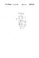
- FIG. 1is a schematic diagram illustrating the process and apparatus for forming a metallic patterned film according to the invention.
- FIG. 2is a block diagram showing the converging ion beam generator.
- the converging ion beam generator 1is shown in FIG. 2.
- the substance 30 to be ionizedis, made Ga metal, which is surrounded by a heater 31 to heat and fuse the surface only.
- the fused Ga metalis extracted by the extracting electrode 32 so that it is converted into Ga ions.
- the Ga ionsare further heated by the heating electrode 33.
- the heated Ga ionsare converged or focused into a focused metal ion beam by the converging lens system 34.
- the ion beam directed to the substrateis turned on and off by the blanking electrode 35.
- the converging ion beam generator 21is disposed in a vacuum chamber 21 connected to the vacuum pump 10.
- the ion beam 3 generated and controlled as mentioned aboveis irradicated onto the substrate 4 placed on the cooling plate 16 supported by the X-Y stage through the insulator 17.
- the ion beam 3is caused to scan the substrate 4 by the deflection electrode 2 (for the X and Y directions).
- the secondary charged particles released from the surface of the substrate 4are detected by the secondary charged particles detector 6.
- the detected informationis converted into brightness signals after amplification and processing by the signal amplifier/processor 14.
- the signals together with the scanning signal from the scanning controller 12 enterare applied to the display 15, on which the image of secondary charged particles is displayed.
- the image of secondary charged particlesis used to locate the position on the substrate 4 where the metallic patterned film is to be made, and the area for the metallic patterned film is designated by the scanning range setting unit 13.
- the valve 8 of the gas gun 7Upon receipt of a signal for the start of deposition, the valve 8 of the gas gun 7 is opened and the vapor stream of hexacarbonyl metal is directed toward the surface of the substrate 4. At this time, the gas source 9 is heated at a prescribed temperature by a heater, and the substrate 4 is kept cooled at a prescribed temperature by the cooling plate 16 connected to the cooler 19. Thus, the surface of the substrate 4 which has adsorbed the vapor of hexacarbonyl metal is irradiated with the converging ion beam which is controlled by the scanning range setting unit 13 with respect to a scanning range and scanning frequency.
- the hexacarbonyl metalis decomposed with the result that CO gas component dissipates into the vacuum or the vacuum chamber 21 and the metal component deposits on the surface of the substrate.
- the scanning of the converging ion beam 3is repeated while the vapor of hexacarbonyl metal is continuously supplied, there is formed a metallic patterned film having a thickness proportional to the number of repeated.
- the source gas for film formationis a hexacarbonyl metal vapor instead of the conventional metal halide vapor.
- the hexacarbonyl metal vaporcan be effectively adsorbed by the surface of the substrate at a temperature slightly lower than room temperature, without being cooled to the liquefied nitrogen temperature. This leads to the faster film growth and the formation of film superior in conductivity and film adhesion.
- the source gasis W(CO) 6 and the converging ion beam is of Ga ions
- the resulting filmhas a specific resistance of about 10 -4 to 10 -5 ⁇ cm and submicron lines of pattern can be obtained.
- the filmis composed mainly of W, and it contains very little oxygen joined bonded to Ga and C.
- the filmhas sufficiently high hardness and adhesion. Therefore, the film formed by the process of this invention is suitable for forming new wiring routes or paths on a semiconductor device and for repairing a defective metallic pattern on an X-ray mask.
- the converging ion beamshould be of heavy metal ions (such as Au ions, Bi ions, and Pb ions) and the source gas should be W(CO) 6 so that there is formed a film having a greater coefficient of X-ray absorption.
Landscapes
- Engineering & Computer Science (AREA)
- Chemical & Material Sciences (AREA)
- Physics & Mathematics (AREA)
- Condensed Matter Physics & Semiconductors (AREA)
- General Physics & Mathematics (AREA)
- Manufacturing & Machinery (AREA)
- Computer Hardware Design (AREA)
- Microelectronics & Electronic Packaging (AREA)
- Power Engineering (AREA)
- General Chemical & Material Sciences (AREA)
- Chemical Kinetics & Catalysis (AREA)
- Materials Engineering (AREA)
- Mechanical Engineering (AREA)
- Metallurgy (AREA)
- Organic Chemistry (AREA)
- Health & Medical Sciences (AREA)
- Toxicology (AREA)
- Preparing Plates And Mask In Photomechanical Process (AREA)
- Internal Circuitry In Semiconductor Integrated Circuit Devices (AREA)
- Chemical Vapour Deposition (AREA)
- Exposure And Positioning Against Photoresist Photosensitive Materials (AREA)
- Exposure Of Semiconductors, Excluding Electron Or Ion Beam Exposure (AREA)
Abstract
Description
The present invention relates to a process and apparatus for additionally forming a metallic patterned film on a semiconductor device for wiring or on an exposure photomask (and X-ray mask) for light shielding. The process and apparatus are used to change wiring routes or detect defective wiring on a semiconductor device or to repair defects or change patterns on a photomask.
There is disclosed in "Semiconductor World" (January 1986, pp. 97-100, by M. Yamamoto) a process and apparatus for repairing the photomask by using a converging ion beam. The process and apparatus is used to form a carbon film useful as a light-shielding film of an optical lithography mask. The ion beam is also used to form a metallic patterned film. The result of investigations in this field is reported in "The 17th Symposium on Ion Implantation and Submicron Fabrication" by D. Takehara et al., March 1986, pp. 153-156. According to this report, the converging ion beam is replaced by a broad rare gas ion beam, and WF6 or Ta(OC2 H5)5 is used as a source gas, whereby a film of W or Ta is formed. The thus formed film contains such a large amount of oxygen and has such a high specific resistance of about 1 Ω·cm that it is not suitable for wiring.
As mentioned above, the prior art is capable of performing maskless film deposition with an ion beam, but is not capable of forming a fine metallic patterned film suitable for adding or changing wiring routes on a semiconductor device or for repairing defects in a metal pattern for X-ray mask.
The present invention aims to solve the above-mentioned problems. The means to solve the problems is comprised of a converging ion beam generator, a deflecting electrode to deflect the converging ion beam for scanning, an X-Y stage on which is placed a substrate to be irradiated with the converging ion beam, a gas gun to blow a direct vapor stream of a carbonyl metal compound in the form of a hexacarbonyl metal toward the substrate locally in the vicinity of the area irradiated with the converging ion beam, and a mechanism to cool the substrate. The hexacarbonyl metal is W(CO)6, Mo(CO)6, or Cr(CO)6. The source gas of the gas gun is heated to +40° to +60° C. The substrate is kept cooled at a prescribed temperature in the range of +25° to -50° C. The ion particles for the converging ion beam are any of Ga ion, Au ion, Bi ion, or Pb ion which are readily obtained from a fused metal ion source.
The means constructed as mentioned above functions in the following manner. The gas gun effectively directs a vapor of hexacarbonyl metal toward a substrate locally in the area or in the vicinity of the area irradiated with the ion beam. The vapor of hexacarbonyl metal is adsorbed on the substrate surface because the substrate is cooled by the cooling mechanism. The substrate surface which has adsorbed the hexacarbonyl metal is then irradiated with the converging ion beam which is generated by the converging ion beam generator and is converged and controlled for scanning by the deflection electrode, scanning controller, and scanning area setting device. While the vapor of hexacarbonyl metal is continuously supplied, the scanning of the converging ion beam is repeated. This process forms a metallic patterned film having a film thickness proportional to the repeating number of scanning.
It is an object of the invention to provide a fine metallic pattern on a substrate for a X-ray mask or a semiconductor device.
Other and further objects, features and advantages of the invention will appear more fully from the following description.
FIG. 1 is a schematic diagram illustrating the process and apparatus for forming a metallic patterned film according to the invention; and
FIG. 2 is a block diagram showing the converging ion beam generator.
The invention is described in more detail with reference to the accompanying drawings.
The convergingion beam generator 1 is shown in FIG. 2. Thesubstance 30 to be ionized is, made Ga metal, which is surrounded by aheater 31 to heat and fuse the surface only. The fused Ga metal is extracted by the extractingelectrode 32 so that it is converted into Ga ions. The Ga ions are further heated by theheating electrode 33. The heated Ga ions are converged or focused into a focused metal ion beam by theconverging lens system 34. The ion beam directed to the substrate is turned on and off by theblanking electrode 35. The convergingion beam generator 21 is disposed in avacuum chamber 21 connected to the vacuum pump 10.
Theion beam 3 generated and controlled as mentioned above is irradicated onto thesubstrate 4 placed on thecooling plate 16 supported by the X-Y stage through theinsulator 17. Theion beam 3 is caused to scan thesubstrate 4 by the deflection electrode 2 (for the X and Y directions). The secondary charged particles released from the surface of thesubstrate 4 are detected by the secondarycharged particles detector 6. The detected information is converted into brightness signals after amplification and processing by the signal amplifier/processor 14. The signals together with the scanning signal from thescanning controller 12 enter are applied to thedisplay 15, on which the image of secondary charged particles is displayed. The image of secondary charged particles is used to locate the position on thesubstrate 4 where the metallic patterned film is to be made, and the area for the metallic patterned film is designated by the scanningrange setting unit 13. Upon receipt of a signal for the start of deposition, the valve 8 of the gas gun 7 is opened and the vapor stream of hexacarbonyl metal is directed toward the surface of thesubstrate 4. At this time, thegas source 9 is heated at a prescribed temperature by a heater, and thesubstrate 4 is kept cooled at a prescribed temperature by thecooling plate 16 connected to thecooler 19. Thus, the surface of thesubstrate 4 which has adsorbed the vapor of hexacarbonyl metal is irradiated with the converging ion beam which is controlled by the scanningrange setting unit 13 with respect to a scanning range and scanning frequency. In the area irradiated with the converging ion beam, the hexacarbonyl metal is decomposed with the result that CO gas component dissipates into the vacuum or thevacuum chamber 21 and the metal component deposits on the surface of the substrate. When the scanning of the convergingion beam 3 is repeated while the vapor of hexacarbonyl metal is continuously supplied, there is formed a metallic patterned film having a thickness proportional to the number of repeated.
According to the present invention, the source gas for film formation is a hexacarbonyl metal vapor instead of the conventional metal halide vapor. The hexacarbonyl metal vapor can be effectively adsorbed by the surface of the substrate at a temperature slightly lower than room temperature, without being cooled to the liquefied nitrogen temperature. This leads to the faster film growth and the formation of film superior in conductivity and film adhesion. In an example in which the source gas is W(CO)6 and the converging ion beam is of Ga ions, the resulting film has a specific resistance of about 10-4 to 10-5 Ω·cm and submicron lines of pattern can be obtained. The film is composed mainly of W, and it contains very little oxygen joined bonded to Ga and C. In addition, the film has sufficiently high hardness and adhesion. Therefore, the film formed by the process of this invention is suitable for forming new wiring routes or paths on a semiconductor device and for repairing a defective metallic pattern on an X-ray mask. For the repair of an X-ray mask, the converging ion beam should be of heavy metal ions (such as Au ions, Bi ions, and Pb ions) and the source gas should be W(CO)6 so that there is formed a film having a greater coefficient of X-ray absorption.
Claims (22)
1. A process for forming a new wiring path on a semiconductor device, comprising: providing a semiconductor device having a designated area on which a new wiring path is to be formed; forming a layer of decomposable carbonyl metal compound composed of carbonyl and metal components on the designated area of the semiconductor device by directing a vapor stream of decomposable carbonyl metal compound onto the designated area; and converting the layer of decomposable carbonyl metal compound into a new wiring path on the designated area of the semiconductor device by irradiating the layer with a focused ion beam to decompose the carbonyl metal compound layer into a gaseous carbonyl component which dissipates and a solid metal component which deposits as the new wiring path on the semiconductor device.
2. A process according to claim 1; wherein the decomposable carbonyl metal compound comprises a hexacarbonyl metal compound.
3. A process according to claim 1; wherein the decomposable carbonyl metal compound has a metal component selected from the group consisting of W, Mo and Cr.
4. A process according to claim 1; wherein the focused ion beam is composed of ions selected from the group consisting of Ga ions, Au ions, Bi ions and Pb ions.
5. A process according to claim 1; including cooling the semiconductor device prior to irradiation by the focused ion beam to promote the formation of the layer of carbonyl metal compound.
6. A process for forming a new wiring route on a semiconductor device by using an apparatus which has an ion beam generator comprised of a metal ion source for generating an ion beam, a focusing lens system to focus the ion beam from the metal ion source, a blanking electrode to turn on and off the ion beam, a deflecting electrode to deflect the focused ion beam for scanning the same, an X-Y stage movable in the X-Y directions for mounting thereon a semiconductor device to be irradiated with the focused ion beam, a gas gun to direct a hexacarbonyl metal gas stream against the surface of the semiconductor device where the focused ion beam is irradiated, a gas source to supply hexacarbonyl metal gas to the gas gun, and a detector for detecting secondary charged particles which are generated by the irradiation of the semiconductor device with the focused ion beam, the process comprising the steps of: directing a vapor stream of hexacarbonyl metal toward a predetermined surface portion of the semiconductor device at which a new wiring route is to be formed; and irradiating the predetermined surface portion on which the hexacarbonyl metal is adsorbed with a focused ion beam to thereby decompose the hexacarbonyl metal to deposit a new wiring route on the predetermined surface portion of the semiconductor device.
7. A process as claimed in claim 6; wherein the focused ion beam is composed of Ga ions, Au ions, Bi ions or Pb ions.
8. A process as claimed in claim 6; wherein the hexacarbonyl metal comprises W(CO)6, Mo(CO)6 or Cr(CO)6.
9. A process for forming a new wiring path on a semiconductor device, comprising the steps of: providing a semiconductor device; designating an area of the semiconductor device on which a new wiring path is to be formed; forming a vapor stream of a decomposable carbonyl metal compound composed of a carbonyl component and a metal component; directing the vapor stream toward the designated area of the semiconductor device to form thereon a layer of the decomposable carbonyl metal compound; and irradiating the layer with an ion beam to decompose the carbonyl metal compound into a gaseous carbonyl component and a solid metal component to thereby deposit the solid metal component as a new wiring path on the designated area of the semiconductor device.
10. A process according to claim 9; wherein the decomposable carbonyl metal compound comprises a hexacarbonyl metal.
11. A process according to claim 10; wherein the decomposable carbonyl metal compound is composed of a metal component selected from the group consisting of W, Mo and Cr.
12. A process according to claim 9; wherein the ion beam is comprised of ion particles of a metal.
13. A process according to claim 11; wherein the metal is selected from the group consisting of Ga, Au, Bi and Pb.
14. A process according to claim 9; including the step of cooling the semiconductor device below room temperature to promote adsorption of the carbonyl metal compound on the designated area thereof to thereby promote the formation of the layer of carbonyl metal compound.
15. A method of forming a new wiring path on a semiconductor device using an apparatus having means defining a chamber for receiving a semiconductor device, directing means operable for directing a vapor stream toward the semiconductor device, and irradiating means operable for irradiating the semiconductor device with a focused ion beam, the method comprising the steps of: mounting a semiconductor device in the chamber; designating a specific area of the semiconductor device at which a new wiring path is to be formed; supplying a vapor of a decomposable carbonyl metal compound composed of a carbonyl component and a metal component to the directing means; operating the directing means to direct a vapor stream of carbonyl metal compound vapor toward the designated area of the semiconductor device to thereby form thereon a layer of the carbonyl metal compound; and operating the irradiating means to irradiate the layer with a focused ion beam to decompose the carbonyl metal compound into a gaseous carbonyl component and a solid metal component so as to deposit the solid metal component as a new wiring path on the designated area of the semiconductor device.
16. A method according to claim 15; wherein the mounting step comprises mounting the semiconductor device displaceably in X and Y directions perpendicular to the direction of irradiation of the ion beam.
17. A method according to claim 15; wherein the supplying step comprises supplying a vapor of a decomposable hexacarbonyl metal.
18. A method according to claim 17; wherein the decomposable hexacarbonyl metal is selected from the group consisting of W(CO)6, Mo(CO)6 and Cr(CO)6.
19. A method according to claim 15; including the step of supplying ion particles of a metal to the irradiating means to enable the same to irradiate the designated area of the semiconductor device with a metal ion beam.
20. A method according to claim 19; wherein the metal is selected from the group consisting of Ga, Au, Bi and Pb.
21. A method according to claim 15; wherein the second operating step includes scanning the focused ion beam within the designated area of the semiconductor device so as to control the thickness of the deposited new wiring path.
22. A method according to claim 15; including the step of cooling the semiconductor device below room temperature to promote adsorption of the carbonyl metal compound on the designated area thereof to thereby promote the formation of the layer of carbonyl metal compound.
Applications Claiming Priority (2)
| Application Number | Priority Date | Filing Date | Title |
|---|---|---|---|
| JP61-124146 | 1986-05-29 | ||
| JP61124146AJPS62281349A (en) | 1986-05-29 | 1986-05-29 | Formation of metallic pattern film and apparatus therefor |
Publications (1)
| Publication Number | Publication Date |
|---|---|
| US4876112Atrue US4876112A (en) | 1989-10-24 |
Family
ID=14878070
Family Applications (1)
| Application Number | Title | Priority Date | Filing Date |
|---|---|---|---|
| US07/031,946Expired - LifetimeUS4876112A (en) | 1986-05-29 | 1987-03-27 | Process for forming metallic patterned film |
Country Status (4)
| Country | Link |
|---|---|
| US (1) | US4876112A (en) |
| EP (1) | EP0247714B1 (en) |
| JP (1) | JPS62281349A (en) |
| DE (1) | DE3788678T2 (en) |
Cited By (52)
| Publication number | Priority date | Publication date | Assignee | Title |
|---|---|---|---|---|
| US5026664A (en)* | 1988-04-07 | 1991-06-25 | Hitachi, Ltd. | Method of providing a semiconductor IC device with an additional conduction path |
| US5055696A (en)* | 1988-08-29 | 1991-10-08 | Hitachi, Ltd. | Multilayered device micro etching method and system |
| US5104684A (en)* | 1990-05-25 | 1992-04-14 | Massachusetts Institute Of Technology | Ion beam induced deposition of metals |
| US5106764A (en)* | 1989-04-10 | 1992-04-21 | At&T Bell Laboratories | Device fabrication |
| US5140164A (en)* | 1991-01-14 | 1992-08-18 | Schlumberger Technologies, Inc. | Ic modification with focused ion beam system |
| WO1992014260A1 (en)* | 1991-02-11 | 1992-08-20 | Microelectronics And Computer Technology Corporation | Method of making semiconductor bonding bumps using metal cluster ion deposition |
| US5188705A (en)* | 1991-04-15 | 1993-02-23 | Fei Company | Method of semiconductor device manufacture |
| US5236747A (en)* | 1990-07-06 | 1993-08-17 | Plasmametal | Process for metallizing a surface |
| US5244538A (en)* | 1991-07-26 | 1993-09-14 | Microelectronics And Computer Technology Corporation | Method of patterning metal on a substrate using direct-write deposition of a mask |
| US5262341A (en)* | 1989-05-19 | 1993-11-16 | Fujitsu Limited | Blanking aperture array and charged particle beam exposure method |
| US5314727A (en)* | 1992-07-28 | 1994-05-24 | Minnesota Mining & Mfg. Co./Regents Of The University Of Minnesota | Chemical vapor deposition of iron, ruthenium, and osmium |
| US5331172A (en)* | 1991-02-11 | 1994-07-19 | Microelectronics And Computer Technology Corporation | Ionized metal cluster beam systems and methods |
| US5376791A (en)* | 1991-04-15 | 1994-12-27 | Fei Company | Secondary ion mass spectometry system |
| US5382315A (en)* | 1991-02-11 | 1995-01-17 | Microelectronics And Computer Technology Corporation | Method of forming etch mask using particle beam deposition |
| US5429989A (en)* | 1994-02-03 | 1995-07-04 | Motorola, Inc. | Process for fabricating a metallization structure in a semiconductor device |
| WO1996000803A1 (en)* | 1994-06-28 | 1996-01-11 | Fei Company | Charged particle deposition of electrically insulating films |
| US5509843A (en)* | 1993-05-19 | 1996-04-23 | Kabushiki Kaisha Toshiba | Method and apparatus for manufacturing needle shaped materials and method for manufacturing a microemitter |
| US5534311A (en)* | 1995-05-31 | 1996-07-09 | The United States Of America As Represented By The Secretary Of The Navy | Production of structures by electrostatically-focused deposition |
| US5607722A (en)* | 1996-02-09 | 1997-03-04 | Micron Technology, Inc. | Process for titanium nitride deposition using five-and six-coordinate titanium complexes |
| US5659057A (en)* | 1996-02-09 | 1997-08-19 | Micron Technology, Inc. | Five- and six-coordinate precursors for titanium nitride deposition |
| US5674409A (en)* | 1995-03-16 | 1997-10-07 | International Business Machines Corporation | Nanolithographic method of forming fine lines |
| US5792270A (en)* | 1993-10-21 | 1998-08-11 | Saxena; Arjun | Apparatus for forming a pattern of nucleation sites |
| US5908947A (en)* | 1996-02-09 | 1999-06-01 | Micron Technology, Inc. | Difunctional amino precursors for the deposition of films comprising metals |
| US5958799A (en)* | 1995-04-13 | 1999-09-28 | North Carolina State University | Method for water vapor enhanced charged-particle-beam machining |
| US5976976A (en)* | 1997-08-21 | 1999-11-02 | Micron Technology, Inc. | Method of forming titanium silicide and titanium by chemical vapor deposition |
| DE4110118C2 (en)* | 1990-03-28 | 1999-12-09 | Seiko Instr Inc | Gas gun for an ion beam processing device and its use |
| US6025243A (en)* | 1989-09-26 | 2000-02-15 | Canon Kabushiki Kaisha | Method for preparing a semiconductor device |
| US6143362A (en)* | 1998-02-25 | 2000-11-07 | Micron Technology, Inc. | Chemical vapor deposition of titanium |
| US6261850B1 (en) | 1998-09-03 | 2001-07-17 | Micron Technology, Inc. | Direct writing of low carbon conductive material |
| US6284316B1 (en) | 1998-02-25 | 2001-09-04 | Micron Technology, Inc. | Chemical vapor deposition of titanium |
| EP1063695A3 (en)* | 1999-06-23 | 2001-09-05 | Lucent Technologies Inc. | Method of passivating copper interconnects in a semiconductor device |
| US6395347B1 (en)* | 1993-11-30 | 2002-05-28 | Seiko Instruments Inc. | Micromachining method for workpiece observation |
| US6492261B2 (en)* | 2000-12-30 | 2002-12-10 | Intel Corporation | Focused ion beam metal deposition |
| WO2002059926A3 (en)* | 2001-01-26 | 2003-01-09 | Fei Co | Fabrication of high resistivity structures using focused ion beams |
| US6638580B2 (en)* | 2000-12-29 | 2003-10-28 | Intel Corporation | Apparatus and a method for forming an alloy layer over a substrate using an ion beam |
| US20040065826A1 (en)* | 2000-02-25 | 2004-04-08 | Steve Berger | System for imaging a cross-section of a substrate |
| US20040099636A1 (en)* | 2002-11-21 | 2004-05-27 | Lawrence Scipioni | Fabrication of three dimensional structures |
| US20040140438A1 (en)* | 2001-01-19 | 2004-07-22 | Gerlach Robert L. | Angular aperture shaped beam system and method |
| US6864481B2 (en)* | 2001-12-04 | 2005-03-08 | Sii Nanotechnology Inc. | Probe for scanning probe microscope |
| US6949756B2 (en) | 2000-01-21 | 2005-09-27 | Fei Company | Shaped and low density focused ion beams |
| US20050227484A1 (en)* | 2004-04-13 | 2005-10-13 | Fei Company | System for modifying small structures |
| US20060051508A1 (en)* | 2000-12-28 | 2006-03-09 | Ilan Gavish | Focused ion beam deposition |
| US20060068096A1 (en)* | 2001-12-12 | 2006-03-30 | Electrovac, Fabrikation Elektrotechnischer Spezialartikel Gesellschaft M.B.H. | Method of synthesising carbon nano tubes |
| US7258901B1 (en)* | 2000-09-08 | 2007-08-21 | Fei Company | Directed growth of nanotubes on a catalyst |
| US20100068408A1 (en)* | 2008-09-16 | 2010-03-18 | Omniprobe, Inc. | Methods for electron-beam induced deposition of material inside energetic-beam microscopes |
| US20110070381A1 (en)* | 2009-09-23 | 2011-03-24 | Fei Company | Use of nitrogen-based reducing compounds in beam-induced processing |
| EP2570519A2 (en) | 2011-09-19 | 2013-03-20 | Fei Company | Localized, In-Vacuum Modification of Small Structures |
| CN103855083A (en)* | 2012-12-04 | 2014-06-11 | Fei公司 | Microfluidics delivery systems |
| US9514913B2 (en) | 2014-07-21 | 2016-12-06 | Fei Company | TEM sample mounting geometry |
| EP3125270A1 (en) | 2015-07-27 | 2017-02-01 | FEI Company | Tem sample mounting geometry |
| ES2738911A1 (en)* | 2018-07-25 | 2020-01-27 | Consejo Superior Investigacion | PROCEDURE FOR DEPOSITING ELEMENTS ON A SUBSTRATE OF INTEREST AND DEVICE (Machine-translation by Google Translate, not legally binding) |
| US12252778B2 (en)* | 2019-03-20 | 2025-03-18 | Samsung Electronics Co, Ltd. | Apparatus for and method of manufacturing semiconductor device |
Families Citing this family (4)
| Publication number | Priority date | Publication date | Assignee | Title |
|---|---|---|---|---|
| JPH0664338B2 (en)* | 1988-02-02 | 1994-08-22 | 三菱電機株式会社 | Method for correcting thin film pattern and exposure mask modified by the method |
| US4908226A (en)* | 1988-05-23 | 1990-03-13 | Hughes Aircraft Company | Selective area nucleation and growth method for metal chemical vapor deposition using focused ion beams |
| DE69132474T2 (en)* | 1990-05-31 | 2001-05-03 | Canon K.K., Tokio/Tokyo | Method for wiring a semiconductor device |
| JP2771472B2 (en) | 1994-05-16 | 1998-07-02 | 松下電器産業株式会社 | Method for manufacturing semiconductor device |
Citations (7)
| Publication number | Priority date | Publication date | Assignee | Title |
|---|---|---|---|---|
| US4042006A (en)* | 1973-01-05 | 1977-08-16 | Siemens Aktiengesellschaft | Pyrolytic process for producing a band-shaped metal layer on a substrate |
| US4372989A (en)* | 1979-06-20 | 1983-02-08 | Siemens Aktiengesellschaft | Process for producing coarse-grain crystalline/mono-crystalline metal and alloy films |
| JPS60182726A (en)* | 1984-02-29 | 1985-09-18 | Seiko Instr & Electronics Ltd | Forming method of pattern film |
| US4609809A (en)* | 1983-03-16 | 1986-09-02 | Hitachi, Ltd. | Method and apparatus for correcting delicate wiring of IC device |
| US4612085A (en)* | 1985-04-10 | 1986-09-16 | Texas Instruments Incorporated | Photochemical patterning |
| US4615904A (en)* | 1982-06-01 | 1986-10-07 | Massachusetts Institute Of Technology | Maskless growth of patterned films |
| JPH0694728A (en)* | 1992-09-09 | 1994-04-08 | Shimadzu Corp | Clinical testing equipment sample pallet |
Family Cites Families (4)
| Publication number | Priority date | Publication date | Assignee | Title |
|---|---|---|---|---|
| US4451503A (en)* | 1982-06-30 | 1984-05-29 | International Business Machines Corporation | Photo deposition of metals with far UV radiation |
| DE3483982D1 (en)* | 1983-06-29 | 1991-02-28 | Siemens Ag | METHOD FOR PRODUCING AN ELECTRICALLY CONDUCTIVE CONNECTION AND DEVICE FOR CARRYING OUT SUCH A METHOD. |
| JPS60245227A (en)* | 1984-05-21 | 1985-12-05 | Seiko Instr & Electronics Ltd | Pattern film forming method |
| JPH0763064B2 (en)* | 1986-03-31 | 1995-07-05 | 株式会社日立製作所 | Wiring connection method for IC element |
- 1986
- 1986-05-29JPJP61124146Apatent/JPS62281349A/enactivePending
- 1987
- 1987-03-27USUS07/031,946patent/US4876112A/ennot_activeExpired - Lifetime
- 1987-04-06EPEP87302981Apatent/EP0247714B1/ennot_activeExpired - Lifetime
- 1987-04-06DEDE87302981Tpatent/DE3788678T2/ennot_activeExpired - Lifetime
Patent Citations (8)
| Publication number | Priority date | Publication date | Assignee | Title |
|---|---|---|---|---|
| US4042006A (en)* | 1973-01-05 | 1977-08-16 | Siemens Aktiengesellschaft | Pyrolytic process for producing a band-shaped metal layer on a substrate |
| US4372989A (en)* | 1979-06-20 | 1983-02-08 | Siemens Aktiengesellschaft | Process for producing coarse-grain crystalline/mono-crystalline metal and alloy films |
| US4615904A (en)* | 1982-06-01 | 1986-10-07 | Massachusetts Institute Of Technology | Maskless growth of patterned films |
| US4609809A (en)* | 1983-03-16 | 1986-09-02 | Hitachi, Ltd. | Method and apparatus for correcting delicate wiring of IC device |
| US4609809B1 (en)* | 1983-03-16 | 1993-01-26 | Hitachi Ltd | |
| JPS60182726A (en)* | 1984-02-29 | 1985-09-18 | Seiko Instr & Electronics Ltd | Forming method of pattern film |
| US4612085A (en)* | 1985-04-10 | 1986-09-16 | Texas Instruments Incorporated | Photochemical patterning |
| JPH0694728A (en)* | 1992-09-09 | 1994-04-08 | Shimadzu Corp | Clinical testing equipment sample pallet |
Cited By (97)
| Publication number | Priority date | Publication date | Assignee | Title |
|---|---|---|---|---|
| US5026664A (en)* | 1988-04-07 | 1991-06-25 | Hitachi, Ltd. | Method of providing a semiconductor IC device with an additional conduction path |
| US5055696A (en)* | 1988-08-29 | 1991-10-08 | Hitachi, Ltd. | Multilayered device micro etching method and system |
| US5106764A (en)* | 1989-04-10 | 1992-04-21 | At&T Bell Laboratories | Device fabrication |
| US5262341A (en)* | 1989-05-19 | 1993-11-16 | Fujitsu Limited | Blanking aperture array and charged particle beam exposure method |
| US6025243A (en)* | 1989-09-26 | 2000-02-15 | Canon Kabushiki Kaisha | Method for preparing a semiconductor device |
| DE4110118C2 (en)* | 1990-03-28 | 1999-12-09 | Seiko Instr Inc | Gas gun for an ion beam processing device and its use |
| US5104684A (en)* | 1990-05-25 | 1992-04-14 | Massachusetts Institute Of Technology | Ion beam induced deposition of metals |
| US5236747A (en)* | 1990-07-06 | 1993-08-17 | Plasmametal | Process for metallizing a surface |
| US5140164A (en)* | 1991-01-14 | 1992-08-18 | Schlumberger Technologies, Inc. | Ic modification with focused ion beam system |
| WO1992014260A1 (en)* | 1991-02-11 | 1992-08-20 | Microelectronics And Computer Technology Corporation | Method of making semiconductor bonding bumps using metal cluster ion deposition |
| US5156997A (en)* | 1991-02-11 | 1992-10-20 | Microelectronics And Computer Technology Corporation | Method of making semiconductor bonding bumps using metal cluster ion deposition |
| US5382315A (en)* | 1991-02-11 | 1995-01-17 | Microelectronics And Computer Technology Corporation | Method of forming etch mask using particle beam deposition |
| US5290732A (en)* | 1991-02-11 | 1994-03-01 | Microelectronics And Computer Technology Corporation | Process for making semiconductor electrode bumps by metal cluster ion deposition and etching |
| US5331172A (en)* | 1991-02-11 | 1994-07-19 | Microelectronics And Computer Technology Corporation | Ionized metal cluster beam systems and methods |
| US5188705A (en)* | 1991-04-15 | 1993-02-23 | Fei Company | Method of semiconductor device manufacture |
| US5376791A (en)* | 1991-04-15 | 1994-12-27 | Fei Company | Secondary ion mass spectometry system |
| US5244538A (en)* | 1991-07-26 | 1993-09-14 | Microelectronics And Computer Technology Corporation | Method of patterning metal on a substrate using direct-write deposition of a mask |
| US5314727A (en)* | 1992-07-28 | 1994-05-24 | Minnesota Mining & Mfg. Co./Regents Of The University Of Minnesota | Chemical vapor deposition of iron, ruthenium, and osmium |
| US5372849A (en)* | 1992-07-28 | 1994-12-13 | Minnesota Mining And Manufacturing Company | Chemical vapor deposition of iron, ruthenium, and osmium |
| US5509843A (en)* | 1993-05-19 | 1996-04-23 | Kabushiki Kaisha Toshiba | Method and apparatus for manufacturing needle shaped materials and method for manufacturing a microemitter |
| US5792270A (en)* | 1993-10-21 | 1998-08-11 | Saxena; Arjun | Apparatus for forming a pattern of nucleation sites |
| US6395347B1 (en)* | 1993-11-30 | 2002-05-28 | Seiko Instruments Inc. | Micromachining method for workpiece observation |
| US5429989A (en)* | 1994-02-03 | 1995-07-04 | Motorola, Inc. | Process for fabricating a metallization structure in a semiconductor device |
| WO1996000803A1 (en)* | 1994-06-28 | 1996-01-11 | Fei Company | Charged particle deposition of electrically insulating films |
| US5827786A (en)* | 1994-06-28 | 1998-10-27 | Fei Company | Charged particle deposition of electrically insulating films |
| US5674409A (en)* | 1995-03-16 | 1997-10-07 | International Business Machines Corporation | Nanolithographic method of forming fine lines |
| US6140655A (en)* | 1995-04-13 | 2000-10-31 | North Carolina State University | Method for water vapor enhanced charged-particle-beam machining |
| US5958799A (en)* | 1995-04-13 | 1999-09-28 | North Carolina State University | Method for water vapor enhanced charged-particle-beam machining |
| US5534311A (en)* | 1995-05-31 | 1996-07-09 | The United States Of America As Represented By The Secretary Of The Navy | Production of structures by electrostatically-focused deposition |
| US5908947A (en)* | 1996-02-09 | 1999-06-01 | Micron Technology, Inc. | Difunctional amino precursors for the deposition of films comprising metals |
| US5659057A (en)* | 1996-02-09 | 1997-08-19 | Micron Technology, Inc. | Five- and six-coordinate precursors for titanium nitride deposition |
| US5607722A (en)* | 1996-02-09 | 1997-03-04 | Micron Technology, Inc. | Process for titanium nitride deposition using five-and six-coordinate titanium complexes |
| US5866205A (en)* | 1996-02-09 | 1999-02-02 | Micron Technology, Inc. | Process for titanium nitride deposition using five- and six-coordinate titanium complexes |
| US5976976A (en)* | 1997-08-21 | 1999-11-02 | Micron Technology, Inc. | Method of forming titanium silicide and titanium by chemical vapor deposition |
| US6171943B1 (en) | 1997-08-21 | 2001-01-09 | Micron, Technology, Inc. | Methods of forming a contact having titanium silicide formed by chemical vapor deposition |
| US6208033B1 (en) | 1997-08-21 | 2001-03-27 | Micron Technology Inc. | Apparatus having titanium silicide and titanium formed by chemical vapor deposition |
| US6255209B1 (en) | 1997-08-21 | 2001-07-03 | Micron Technology, Inc. | Methods of forming a contact having titanium formed by chemical vapor deposition |
| US6255216B1 (en) | 1997-08-21 | 2001-07-03 | Micron Technology, Inc. | Methods of forming a contact having titanium silicide and titanium formed by chemical vapor deposition |
| US6472756B2 (en) | 1997-08-21 | 2002-10-29 | Micron Technology, Inc. | Method of forming titanium silicide and titanium by chemical vapor deposition and resulting apparatus |
| US8456007B2 (en) | 1998-02-25 | 2013-06-04 | Round Rock Research, Llc | Chemical vapor deposition of titanium |
| US6830838B2 (en) | 1998-02-25 | 2004-12-14 | Micron Technology, Inc. | Chemical vapor deposition of titanium |
| US6284316B1 (en) | 1998-02-25 | 2001-09-04 | Micron Technology, Inc. | Chemical vapor deposition of titanium |
| US6940172B2 (en) | 1998-02-25 | 2005-09-06 | Micron Technology, Inc. | Chemical vapor deposition of titanium |
| US20050255698A1 (en)* | 1998-02-25 | 2005-11-17 | Micron Technology, Inc. | Chemical vapor deposition of titanim |
| US6143362A (en)* | 1998-02-25 | 2000-11-07 | Micron Technology, Inc. | Chemical vapor deposition of titanium |
| US20090039517A1 (en)* | 1998-02-25 | 2009-02-12 | Micron Technology, Inc. | Chemical vapor deposition of titanium |
| US7443032B2 (en) | 1998-02-25 | 2008-10-28 | Micron Technology, Inc. | Memory device with chemical vapor deposition of titanium for titanium silicide contacts |
| US6903462B2 (en) | 1998-02-25 | 2005-06-07 | Micron Technology, Inc. | Chemical vapor deposition of titanium |
| US6830820B2 (en) | 1998-02-25 | 2004-12-14 | Micron Technology, Inc. | Chemical vapor deposition of titanium |
| US6261850B1 (en) | 1998-09-03 | 2001-07-17 | Micron Technology, Inc. | Direct writing of low carbon conductive material |
| US6455423B2 (en) | 1998-09-03 | 2002-09-24 | Micron Technology, Inc. | Direct writing of low carbon conductive material |
| EP1063695A3 (en)* | 1999-06-23 | 2001-09-05 | Lucent Technologies Inc. | Method of passivating copper interconnects in a semiconductor device |
| US6949756B2 (en) | 2000-01-21 | 2005-09-27 | Fei Company | Shaped and low density focused ion beams |
| US6727500B1 (en) | 2000-02-25 | 2004-04-27 | Fei Company | System for imaging a cross-section of a substrate |
| US20040065826A1 (en)* | 2000-02-25 | 2004-04-08 | Steve Berger | System for imaging a cross-section of a substrate |
| US6838668B2 (en) | 2000-02-25 | 2005-01-04 | Fei Company | System for imaging a cross-section of a substrate |
| US7258901B1 (en)* | 2000-09-08 | 2007-08-21 | Fei Company | Directed growth of nanotubes on a catalyst |
| US20060051508A1 (en)* | 2000-12-28 | 2006-03-09 | Ilan Gavish | Focused ion beam deposition |
| US20040016403A1 (en)* | 2000-12-29 | 2004-01-29 | Dan Gavish | Apparatus and a method for forming an alloy layer over a substrate |
| US20020197851A1 (en)* | 2000-12-29 | 2002-12-26 | Ilan Gavish | Focused ion beam deposition |
| US7171918B2 (en) | 2000-12-29 | 2007-02-06 | Intel Corporation | Focused ion beam deposition |
| US20060252255A9 (en)* | 2000-12-29 | 2006-11-09 | Ilan Gavish | Focused ion beam deposition |
| US20060051950A1 (en)* | 2000-12-29 | 2006-03-09 | Iian Gavish | Apparatus and a method for forming an alloy layer over a substrate |
| US6638580B2 (en)* | 2000-12-29 | 2003-10-28 | Intel Corporation | Apparatus and a method for forming an alloy layer over a substrate using an ion beam |
| US6957624B2 (en) | 2000-12-29 | 2005-10-25 | Intel Corporation | Apparatus and a method for forming an alloy layer over a substrate |
| US20050252453A1 (en)* | 2000-12-29 | 2005-11-17 | Dan Gavish | Apparatus and a method for forming an alloy layer over a substrate |
| US6492261B2 (en)* | 2000-12-30 | 2002-12-10 | Intel Corporation | Focused ion beam metal deposition |
| US20040020434A1 (en)* | 2000-12-30 | 2004-02-05 | Ilan Gavish | Focused ion beam deposition |
| US6627538B2 (en) | 2000-12-30 | 2003-09-30 | Intel Corporation | Focused ion beam deposition |
| US20040140438A1 (en)* | 2001-01-19 | 2004-07-22 | Gerlach Robert L. | Angular aperture shaped beam system and method |
| US6838380B2 (en) | 2001-01-26 | 2005-01-04 | Fei Company | Fabrication of high resistivity structures using focused ion beams |
| WO2002059926A3 (en)* | 2001-01-26 | 2003-01-09 | Fei Co | Fabrication of high resistivity structures using focused ion beams |
| US6864481B2 (en)* | 2001-12-04 | 2005-03-08 | Sii Nanotechnology Inc. | Probe for scanning probe microscope |
| US20060068096A1 (en)* | 2001-12-12 | 2006-03-30 | Electrovac, Fabrikation Elektrotechnischer Spezialartikel Gesellschaft M.B.H. | Method of synthesising carbon nano tubes |
| US7033647B2 (en)* | 2001-12-12 | 2006-04-25 | Electrovac, Fabrikation Elektrotechnischer Spezialartikel Gesellschaft M.B.H. | Method of synthesising carbon nano tubes |
| US20040099636A1 (en)* | 2002-11-21 | 2004-05-27 | Lawrence Scipioni | Fabrication of three dimensional structures |
| US7160475B2 (en) | 2002-11-21 | 2007-01-09 | Fei Company | Fabrication of three dimensional structures |
| US20100151679A1 (en)* | 2004-04-13 | 2010-06-17 | Fei Company | System for modifying small structures |
| US20050227484A1 (en)* | 2004-04-13 | 2005-10-13 | Fei Company | System for modifying small structures |
| US8163641B2 (en) | 2004-04-13 | 2012-04-24 | Fei Company | System for modifying small structures |
| EP1610377A2 (en) | 2004-04-13 | 2005-12-28 | FEI Company | System for modifying small structures |
| US7674706B2 (en) | 2004-04-13 | 2010-03-09 | Fei Company | System for modifying small structures using localized charge transfer mechanism to remove or deposit material |
| US20100068408A1 (en)* | 2008-09-16 | 2010-03-18 | Omniprobe, Inc. | Methods for electron-beam induced deposition of material inside energetic-beam microscopes |
| US20110070381A1 (en)* | 2009-09-23 | 2011-03-24 | Fei Company | Use of nitrogen-based reducing compounds in beam-induced processing |
| US8617668B2 (en) | 2009-09-23 | 2013-12-31 | Fei Company | Method of using nitrogen based compounds to reduce contamination in beam-induced thin film deposition |
| US9255339B2 (en) | 2011-09-19 | 2016-02-09 | Fei Company | Localized, in-vacuum modification of small structures |
| EP2570519A2 (en) | 2011-09-19 | 2013-03-20 | Fei Company | Localized, In-Vacuum Modification of Small Structures |
| US9812286B2 (en) | 2011-09-19 | 2017-11-07 | Fei Company | Localized, in-vacuum modification of small structures |
| CN103855083A (en)* | 2012-12-04 | 2014-06-11 | Fei公司 | Microfluidics delivery systems |
| US9044781B2 (en) | 2012-12-04 | 2015-06-02 | Fei Company | Microfluidics delivery systems |
| EP2741075A2 (en) | 2012-12-04 | 2014-06-11 | Fei Company | Method of processing a workpiece in a vacuum chamber |
| CN103855083B (en)* | 2012-12-04 | 2019-07-16 | Fei 公司 | Miniflow body conveying system |
| US9514913B2 (en) | 2014-07-21 | 2016-12-06 | Fei Company | TEM sample mounting geometry |
| EP3125270A1 (en) | 2015-07-27 | 2017-02-01 | FEI Company | Tem sample mounting geometry |
| ES2738911A1 (en)* | 2018-07-25 | 2020-01-27 | Consejo Superior Investigacion | PROCEDURE FOR DEPOSITING ELEMENTS ON A SUBSTRATE OF INTEREST AND DEVICE (Machine-translation by Google Translate, not legally binding) |
| WO2020021149A1 (en)* | 2018-07-25 | 2020-01-30 | Consejo Superior De Investigaciones Científicas | Method for depositing elements on a substrate of interest and device |
| US12252778B2 (en)* | 2019-03-20 | 2025-03-18 | Samsung Electronics Co, Ltd. | Apparatus for and method of manufacturing semiconductor device |
Also Published As
| Publication number | Publication date |
|---|---|
| DE3788678T2 (en) | 1994-04-28 |
| EP0247714B1 (en) | 1994-01-05 |
| EP0247714A2 (en) | 1987-12-02 |
| EP0247714A3 (en) | 1990-12-05 |
| DE3788678D1 (en) | 1994-02-17 |
| JPS62281349A (en) | 1987-12-07 |
Similar Documents
| Publication | Publication Date | Title |
|---|---|---|
| US4876112A (en) | Process for forming metallic patterned film | |
| US4874460A (en) | Method and apparatus for modifying patterned film | |
| EP0199585B1 (en) | Apparatus for depositing electrically conductive and/or electrically insulating material on a workpiece | |
| US5182231A (en) | Method for modifying wiring of semiconductor device | |
| US4778693A (en) | Photolithographic mask repair system | |
| US6344115B1 (en) | Pattern forming method using charged particle beam process and charged particle beam processing system | |
| JPH0425531B2 (en) | ||
| US5026664A (en) | Method of providing a semiconductor IC device with an additional conduction path | |
| JPS6114640A (en) | Method and apparatus for correcting defect of photo mask | |
| US4924104A (en) | Ion beam apparatus and method of modifying substrate | |
| US5004927A (en) | Process for forming a fine pattern having a high aspect ratio | |
| US4902530A (en) | Method of correcting a pattern film | |
| JP3218024B2 (en) | Method and apparatus for forming metal pattern film | |
| JP2939906B1 (en) | Ion beam processing equipment | |
| EP0198908A1 (en) | Focused substrate alteration | |
| JPS61245164A (en) | Pattern correcting device | |
| WO1988009049A1 (en) | Mask repair using an optimized focused ion beam system | |
| JPH10163201A (en) | Pattern forming method and its device | |
| JPH09172013A (en) | Method and apparatus for forming metal pattern film | |
| EP0571727A1 (en) | Apparatus and method for focussed ion beam deposition by controlling beam parameters | |
| JP3013158B2 (en) | Pattern correction method | |
| JP3051909B2 (en) | Pattern film repair method and apparatus | |
| KR19990088454A (en) | Metal pattern film forming method and apparatus therefor | |
| JP2799861B2 (en) | Pattern film correction method | |
| JP2558614B2 (en) | Pattern film generation method |
Legal Events
| Date | Code | Title | Description |
|---|---|---|---|
| AS | Assignment | Owner name:SEIKO INSTRUMENTS INC., JAPAN Free format text:ASSIGNMENT OF ASSIGNORS INTEREST.;ASSIGNORS:KAITO, TAKASHI;ADACHI, TATSUYA;REEL/FRAME:005133/0228 Effective date:19890805 | |
| STCF | Information on status: patent grant | Free format text:PATENTED CASE | |
| FPAY | Fee payment | Year of fee payment:4 | |
| FPAY | Fee payment | Year of fee payment:8 | |
| FPAY | Fee payment | Year of fee payment:12 | |
| AS | Assignment | Owner name:SII NANOTECHNOLOGY INC., JAPAN Free format text:ASSIGNMENT OF ASSIGNORS INTEREST;ASSIGNOR:SEIKO INSTRUMENTS INC.;REEL/FRAME:015711/0053 Effective date:20050128 |