US4875083A - Metal-insulator-semiconductor capacitor formed on silicon carbide - Google Patents
Metal-insulator-semiconductor capacitor formed on silicon carbideDownload PDFInfo
- Publication number
- US4875083A US4875083AUS07/113,572US11357287AUS4875083AUS 4875083 AUS4875083 AUS 4875083AUS 11357287 AUS11357287 AUS 11357287AUS 4875083 AUS4875083 AUS 4875083A
- Authority
- US
- United States
- Prior art keywords
- capacitor according
- silicon carbide
- metal
- silicon
- capacitance
- Prior art date
- Legal status (The legal status is an assumption and is not a legal conclusion. Google has not performed a legal analysis and makes no representation as to the accuracy of the status listed.)
- Expired - Lifetime
Links
Images

Classifications
- H—ELECTRICITY
- H10—SEMICONDUCTOR DEVICES; ELECTRIC SOLID-STATE DEVICES NOT OTHERWISE PROVIDED FOR
- H10D—INORGANIC ELECTRIC SEMICONDUCTOR DEVICES
- H10D62/00—Semiconductor bodies, or regions thereof, of devices having potential barriers
- H10D62/80—Semiconductor bodies, or regions thereof, of devices having potential barriers characterised by the materials
- H10D62/83—Semiconductor bodies, or regions thereof, of devices having potential barriers characterised by the materials being Group IV materials, e.g. B-doped Si or undoped Ge
- H10D62/832—Semiconductor bodies, or regions thereof, of devices having potential barriers characterised by the materials being Group IV materials, e.g. B-doped Si or undoped Ge being Group IV materials comprising two or more elements, e.g. SiGe
- H10D62/8325—Silicon carbide
- G—PHYSICS
- G01—MEASURING; TESTING
- G01N—INVESTIGATING OR ANALYSING MATERIALS BY DETERMINING THEIR CHEMICAL OR PHYSICAL PROPERTIES
- G01N27/00—Investigating or analysing materials by the use of electric, electrochemical, or magnetic means
- G01N27/02—Investigating or analysing materials by the use of electric, electrochemical, or magnetic means by investigating impedance
- G01N27/22—Investigating or analysing materials by the use of electric, electrochemical, or magnetic means by investigating impedance by investigating capacitance
- G01N27/227—Sensors changing capacitance upon adsorption or absorption of fluid components, e.g. electrolyte-insulator-semiconductor sensors, MOS capacitors
- H—ELECTRICITY
- H10—SEMICONDUCTOR DEVICES; ELECTRIC SOLID-STATE DEVICES NOT OTHERWISE PROVIDED FOR
- H10D—INORGANIC ELECTRIC SEMICONDUCTOR DEVICES
- H10D1/00—Resistors, capacitors or inductors
- H10D1/60—Capacitors
- H10D1/62—Capacitors having potential barriers
- H10D1/66—Conductor-insulator-semiconductor capacitors, e.g. MOS capacitors
- H—ELECTRICITY
- H10—SEMICONDUCTOR DEVICES; ELECTRIC SOLID-STATE DEVICES NOT OTHERWISE PROVIDED FOR
- H10D—INORGANIC ELECTRIC SEMICONDUCTOR DEVICES
- H10D64/00—Electrodes of devices having potential barriers
- H10D64/60—Electrodes characterised by their materials
- H—ELECTRICITY
- H10—SEMICONDUCTOR DEVICES; ELECTRIC SOLID-STATE DEVICES NOT OTHERWISE PROVIDED FOR
- H10D—INORGANIC ELECTRIC SEMICONDUCTOR DEVICES
- H10D64/00—Electrodes of devices having potential barriers
- H10D64/60—Electrodes characterised by their materials
- H10D64/62—Electrodes ohmically coupled to a semiconductor
Definitions
- the present inventionrelates to a metal-insulator-semiconductor capacitor, and in particular relates to a metal-oxide-semiconductor capacitor formed on silicon carbide.
- Silicon carbidehas been a perennial candidate for use in semiconductor devices. Silicon carbide has long been recognized as having particular characteristics which give it excellent potential for producing semiconductor devices having superior characteristics to devices formed of other commonly used semiconductor materials such as silicon (Si), gallium arsenide (GaAs), and indium phosphide (InP). Silicon carbide has a wide bandgap, a high melting point, a low dielectric constant, a high breakdown field strength, a high thermal conductivity and a high saturated electron drift velocity. These characteristics give devices made from silicon carbide the potential to operate at higher temperatures, in closer proximity to one another, at higher power levels, and a number of other circumstances under which devices made from other semiconductor materials simply could not perform.
- Silicon carbideis an extremely difficult material to work with which crystallizes in well over 150 different polytypes. Accordingly, forming the large single crystals of a single polytype or the thin films of particular polytypes of silicon carbide which are required to produce electronic devices on semiconductor materials has remained an elusive goal.
- MOS capacitormetal-insulator-semiconductor capacitor
- MOS capacitorscan be used, for example, as temperature sensors, by monitoring the shift in threshold or flatband voltage of the capacitor with changes in temperature. Additionally, at a given temperature, a MOS capacitor can be used as a gas sensor by monitoring the shift in the threshold or flatband voltage as a function of the partial pressure of the gas. Additionally, as stated earlier, MOS capacitors could be used as capacitors in various circuit designs, particularly in conjunction with other devices formed from silicon carbide.
- Shibahara et al.Metal-Oxide-Semiconductor Characteristics of Chemical Vapor Deposited Cubic-SiC, Jap. J. Appl. Phys., Vol. 23, No. 11, 1984, p. L-862, also discuss an aluminum and silicon dioxide MOS capacitor on a 3C silicon carbide thin film. Shibahara, however, made the ohmic contact on the back of a 10 micrometer thin film of silicon carbide after a silicon substrate had been etched off. Such a device design would be far too thin and difficult to handle for any practical commercial applications.
- the capacitorcomprises a semiconductor portion, an active portion of insulated material upon the semiconductor portion, a metal portion upon the insulator portion for defining the active region, and an ohmic contact upon the semiconductor portion and positioned in close proximity to both the active portion of the insulator and the active region of the semiconductor.
- the inventionis a metal-oxide-semiconductor (MOS) capacitor that utilizes silicon carbide as the semiconductor material.
- MOSmetal-oxide-semiconductor
- the capacitorutilizes a circular metal contact on top of an oxide layer on SiC. This design, by placing a large area ohmic contact in close proximity to the silicon carbide region being depleted under the metal oxide contact, greatly reduces series resistance in the device, which in turn increases the capacitance range.
- FIG. 1is a top plan view of an MOS capacitor according to the present invention.
- FIG. 2is a cross-sectional view of the MOS capacitor taken along line 2--2 of FIG. 1;
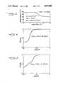
- FIG. 3is a plot of capacitance in picofarads against potential in volts for a capacitor according to the present invention using chromium as the metal in the metal-oxide contact;
- FIG. 4is a similar plot for a capacitor according to the present invention using polycrystalline silicon as the metal in the metal-oxide contact;
- FIG. 5is another plot for a capacitor according to the present invention using polycrystalline silicon as the metal, but with a different dopant density than the capacitor of FIG. 4.
- the inventionis a metal-oxide-semiconductor (MOS) capacitor that utilizes silicon carbide (SiC) as a semiconductor material.
- MOSmetal-oxide-semiconductor
- SiCsilicon carbide
- the inventioncan be formed upon an appropriate silicon carbide crystal of any polytype.
- silicon carbidewhich as discussed earlier is a wide bandgap semiconductor, allows the MOS capacitor of the present invention to operate at much higher temperatures than MOS capacitors formed from silicon or gallium arsenide.
- FIG. 1is a top plan view of an MOS capacitor according to the present invention.
- the metal portion 10is formed of polycrystalline silicon.
- polycrystalline siliconis not a metal, but it is conductive when degenerately doped.
- Polycrystalline siliconis becoming more commonly used for this purpose, but the "metal" terminology used to describe MOS devices, including capacitors and transistors, has remained in use, and for the sake of clarity and consistency will be used herein.
- the design of one preferred embodiment of the inventionis a series of concentric circles.
- the circular metal contact 10is surrounded by the oxide portion 11 which in the illustrated embodiment is a layer of silicon dioxide.
- the oxide layercan be fashioned according to any appropriate technique; for example, thermal oxidation, chemical vapor deposition, or plasma enhanced chemical vapor deposition.
- an ohmic contact 12forms a concentric circle around the oxide portion 11 and the metal contact 10 and in a particular embodiment is formed of tantalum silicide (TaSi 2 ), a novel material for this purpose.
- FIG. 2In a cross-sectional view of FIG. 2, the same elements are visible, along with the silicon carbide portion 13, illustrating that in this embodiment of the invention, the ohmic contact and the active portion of the semiconductor are coplanar with one another upon the surface of the active region of the silicon carbide.
- the metal contact to the oxidecan be selected to be specific to the desired function of the device.
- the metalcan be polysilicon as described above, aluminum, nickel or chromium, among others.
- a temperature sensor corrosion resistant metalsuch as chromium, nickel, platinum, palladium, silver or gold could be used.
- the capacitance of the devicewill be related to both the area of metal-oxide contact and the thickness of the insulator, the diameter of the circular metal contact 10, and the insulator thickness can be selected to obtain a specific capacitance.
- the ohmic contact ring 12is in close proximity to the oxide contact with only a very small gap, typically no more than 50 micrometers, separating them.
- the gap between the ohmic contact 12 and the metal contact 10, and the area outside of the ohmic contact 12,are passivated with the oxide 11, as illustrated in FIG. 2.
- the device designconfines the device to the very top surface of the silicon carbide crystal. This allows the substrate to be of very resistant quality without a concurrent gain in series resistance. Tantalum silicide is used as the ohmic contact, as opposed to typical contacts formed of gold and tantalum alloys, or of nickel, because tantalum silicide is a superior ohmic contact and further aids in the reduction of series resistance.
- FIG. 3is a plot of capacitance in picofarads (pF) versus potential in volts for a metal-oxide-semiconductor capacitor according to the present invention.
- the capacitor of FIG. 3used chromium as the metal in the metal-oxide contact, which contact had an area of 1 ⁇ 10 -3 square centimeters (cm 2 ).
- the carrier concentration of this substratewas 1.9 ⁇ 10 17 cm -3 and the capacitor demonstrated an excellent flatband voltage of -0.25 volts.
- the carrier concentration of a substratewas 1.9 ⁇ 10 17 cm -3 and the fixed oxide charge was 8.64 ⁇ 10 10 cm -2 .
- the resultwas a flatband capacitance of 35.2 picofarads and a ratio of minimum capacitance to maximum capacitance (C min /C max ) of 0.57.
- FIG. 4is a similar plot of the ratio of measured capacitance to the capacitance of the oxide versus potential for a capacitor according to the present invention which used polycrystalline silicon as the conductor in the metal-oxide contact.
- This particular capacitorhad a metal contact area of approximately 2 ⁇ 10 -3 cm -2 , a carrier concentration of 1.72 ⁇ 10 16 cm -3 and a fixed oxide charge of 4.28 ⁇ 10 12 cm -2 .
- the resultwas a capacitor which showed a flatband voltage of -10.6 volts, and a ratio of minimum capacitance to maximum capacitance of 0.264. Minimum capacitance was 36.6 pF and maximum capacitance was 138 pF.
- FIG. 5is another plot of the ratio of measured capacitance to the capacitance of the oxide versus voltage for another capacitance which used polycrystalline silicon as the metal, but with a different carrier density in the semiconductor than the capacitor of FIG. 4.
- This capacitoralso had an area of approximately 2 ⁇ 10 -3 cm -2 , a carrier concentration of 2.61 ⁇ 10 16 cm -3 and a fixed oxide charge of 4.42 ⁇ 10 12 cm -2 . This resulted in a capacitor which demonstrated a flatband voltage of -11.2 volts, and a ratio of minimum capacitance to maximum capacitance of 0.309. Minimum capacitance was 41.6 pF and maximum capacitance was 134 pF.
Landscapes
- Chemical & Material Sciences (AREA)
- Health & Medical Sciences (AREA)
- Analytical Chemistry (AREA)
- Chemical Kinetics & Catalysis (AREA)
- Electrochemistry (AREA)
- Physics & Mathematics (AREA)
- Engineering & Computer Science (AREA)
- Life Sciences & Earth Sciences (AREA)
- Power Engineering (AREA)
- Biochemistry (AREA)
- General Health & Medical Sciences (AREA)
- General Physics & Mathematics (AREA)
- Immunology (AREA)
- Pathology (AREA)
- Semiconductor Integrated Circuits (AREA)
Abstract
Description
Claims (14)
Priority Applications (1)
| Application Number | Priority Date | Filing Date | Title |
|---|---|---|---|
| US07/113,572US4875083A (en) | 1987-10-26 | 1987-10-26 | Metal-insulator-semiconductor capacitor formed on silicon carbide |
Applications Claiming Priority (1)
| Application Number | Priority Date | Filing Date | Title |
|---|---|---|---|
| US07/113,572US4875083A (en) | 1987-10-26 | 1987-10-26 | Metal-insulator-semiconductor capacitor formed on silicon carbide |
Publications (1)
| Publication Number | Publication Date |
|---|---|
| US4875083Atrue US4875083A (en) | 1989-10-17 |
Family
ID=22350215
Family Applications (1)
| Application Number | Title | Priority Date | Filing Date |
|---|---|---|---|
| US07/113,572Expired - LifetimeUS4875083A (en) | 1987-10-26 | 1987-10-26 | Metal-insulator-semiconductor capacitor formed on silicon carbide |
Country Status (1)
| Country | Link |
|---|---|
| US (1) | US4875083A (en) |
Cited By (59)
| Publication number | Priority date | Publication date | Assignee | Title |
|---|---|---|---|---|
| US5184199A (en)* | 1989-06-07 | 1993-02-02 | Sharp Kabushiki Kaisha | Silicon carbide semiconductor device |
| WO1993011540A1 (en)* | 1991-11-26 | 1993-06-10 | Purdue Research Foundation | Nonvolatile random access memory device |
| US5264713A (en)* | 1991-06-14 | 1993-11-23 | Cree Research, Inc. | Junction field-effect transistor formed in silicon carbide |
| USH1287H (en) | 1992-06-16 | 1994-02-01 | The United States Of America As Represented By The Secretary Of The Navy | Ion implanted diamond metal-insulator-semiconductor field effect transistor |
| US5442200A (en)* | 1994-06-03 | 1995-08-15 | Advanced Technology Materials, Inc. | Low resistance, stable ohmic contacts to silcon carbide, and method of making the same |
| WO1996009534A1 (en)* | 1994-09-23 | 1996-03-28 | Forskarpatent I Linköping Ab | Method and device for gas sensing |
| US5510630A (en)* | 1993-10-18 | 1996-04-23 | Westinghouse Electric Corporation | Non-volatile random access memory cell constructed of silicon carbide |
| US5723376A (en)* | 1994-06-23 | 1998-03-03 | Nippondenso Co., Ltd. | Method of manufacturing SiC semiconductor device having double oxide film formation to reduce film defects |
| US5750434A (en)* | 1993-03-22 | 1998-05-12 | Fuji Electric Co. Ltd. | Surface polishing of silicon carbide electronic device substrate using CEO2 |
| US6077619A (en)* | 1994-10-31 | 2000-06-20 | Sullivan; Thomas M. | Polycrystalline silicon carbide ceramic wafer and substrate |
| WO2000013236A3 (en)* | 1998-08-28 | 2000-08-24 | Cree Research Inc | Layered dielectric on silicon carbide semiconductor structures |
| US6153463A (en)* | 1999-07-09 | 2000-11-28 | Macronix International Co., Ltd. | Triple plate capacitor and method for manufacturing |
| US6309766B1 (en) | 1994-10-31 | 2001-10-30 | Thomas M. Sullivan | Polycrystalline silicon carbide ceramic wafer and substrate |
| US20020030191A1 (en)* | 1998-08-28 | 2002-03-14 | Das Mrinal Kanti | High voltage, high temperature capacitor structures and methods of fabricating same |
| US6410445B1 (en) | 1999-01-25 | 2002-06-25 | Appliedsensor Sweden Ab | Manufacturing method for integrated sensor arrays |
| US6528373B2 (en)* | 2001-02-12 | 2003-03-04 | Cree, Inc. | Layered dielectric on silicon carbide semiconductor structures |
| US20030082842A1 (en)* | 2001-10-31 | 2003-05-01 | National Taiwan University | On-chip temperature sensor formed of MOS tunneling diode |
| US6573128B1 (en) | 2000-11-28 | 2003-06-03 | Cree, Inc. | Epitaxial edge termination for silicon carbide Schottky devices and methods of fabricating silicon carbide devices incorporating same |
| US6610366B2 (en) | 2000-10-03 | 2003-08-26 | Cree, Inc. | Method of N2O annealing an oxide layer on a silicon carbide layer |
| US6706114B2 (en) | 2001-05-21 | 2004-03-16 | Cree, Inc. | Methods of fabricating silicon carbide crystals |
| US20040101625A1 (en)* | 2002-08-30 | 2004-05-27 | Das Mrinal Kanti | Nitrogen passivation of interface states in SiO2/SiC structures |
| US20040119076A1 (en)* | 2002-12-20 | 2004-06-24 | Sei-Hyung Ryu | Vertical JFET limited silicon carbide power metal-oxide semiconductor field effect transistors and methods of fabricating vertical JFET limited silicon carbide metal- oxide semiconductor field effect transistors |
| US20040135153A1 (en)* | 2003-01-15 | 2004-07-15 | Sei-Hyung Ryu | Multiple floating guard ring edge termination for silicon carbide devices and methods of fabricating silicon carbide devices incorporating same |
| US6767843B2 (en) | 2000-10-03 | 2004-07-27 | Cree, Inc. | Method of N2O growth of an oxide layer on a silicon carbide layer |
| US20040211980A1 (en)* | 2003-04-24 | 2004-10-28 | Sei-Hyung Ryu | Silicon carbide power devices with self-aligned source and well regions and methods of fabricating same |
| US20040212011A1 (en)* | 2003-04-24 | 2004-10-28 | Sei-Hyung Ryu | Silicon carbide mosfets with integrated antiparallel junction barrier schottky free wheeling diodes and methods of fabricating the same |
| US20050088798A1 (en)* | 2003-10-22 | 2005-04-28 | Erickson Sean C. | Complimentary metal oxide semiconductor capacitor and method for making same |
| US6956238B2 (en) | 2000-10-03 | 2005-10-18 | Cree, Inc. | Silicon carbide power metal-oxide semiconductor field effect transistors having a shorting channel and methods of fabricating silicon carbide metal-oxide semiconductor field effect transistors having a shorting channel |
| US20060006394A1 (en)* | 2004-05-28 | 2006-01-12 | Caracal, Inc. | Silicon carbide Schottky diodes and fabrication method |
| US20060118792A1 (en)* | 2003-01-15 | 2006-06-08 | Sei-Hyung Ryu | Edge termination structures for silicon carbide devices and methods of fabricating silicon carbide devices incorporating same |
| US7067176B2 (en) | 2000-10-03 | 2006-06-27 | Cree, Inc. | Method of fabricating an oxide layer on a silicon carbide layer utilizing an anneal in a hydrogen environment |
| US7727904B2 (en) | 2005-09-16 | 2010-06-01 | Cree, Inc. | Methods of forming SiC MOSFETs with high inversion layer mobility |
| US20100244047A1 (en)* | 2009-03-27 | 2010-09-30 | Cree, Inc. | Methods of Forming Semiconductor Devices Including Epitaxial Layers and Related Structures |
| US8193848B2 (en) | 2009-06-02 | 2012-06-05 | Cree, Inc. | Power switching devices having controllable surge current capabilities |
| US8294507B2 (en) | 2009-05-08 | 2012-10-23 | Cree, Inc. | Wide bandgap bipolar turn-off thyristor having non-negative temperature coefficient and related control circuits |
| US8330244B2 (en) | 2006-08-01 | 2012-12-11 | Cree, Inc. | Semiconductor devices including Schottky diodes having doped regions arranged as islands and methods of fabricating same |
| US8354690B2 (en) | 2009-08-31 | 2013-01-15 | Cree, Inc. | Solid-state pinch off thyristor circuits |
| US8415671B2 (en) | 2010-04-16 | 2013-04-09 | Cree, Inc. | Wide band-gap MOSFETs having a heterojunction under gate trenches thereof and related methods of forming such devices |
| US8432012B2 (en) | 2006-08-01 | 2013-04-30 | Cree, Inc. | Semiconductor devices including schottky diodes having overlapping doped regions and methods of fabricating same |
| US8541787B2 (en) | 2009-07-15 | 2013-09-24 | Cree, Inc. | High breakdown voltage wide band-gap MOS-gated bipolar junction transistors with avalanche capability |
| US8618582B2 (en) | 2011-09-11 | 2013-12-31 | Cree, Inc. | Edge termination structure employing recesses for edge termination elements |
| US8629509B2 (en) | 2009-06-02 | 2014-01-14 | Cree, Inc. | High voltage insulated gate bipolar transistors with minority carrier diverter |
| US8653534B2 (en) | 2008-05-21 | 2014-02-18 | Cree, Inc. | Junction Barrier Schottky diodes with current surge capability |
| US8664665B2 (en) | 2011-09-11 | 2014-03-04 | Cree, Inc. | Schottky diode employing recesses for elements of junction barrier array |
| US8680587B2 (en) | 2011-09-11 | 2014-03-25 | Cree, Inc. | Schottky diode |
| US8710510B2 (en) | 2006-08-17 | 2014-04-29 | Cree, Inc. | High power insulated gate bipolar transistors |
| US8835987B2 (en) | 2007-02-27 | 2014-09-16 | Cree, Inc. | Insulated gate bipolar transistors including current suppressing layers |
| US8901699B2 (en) | 2005-05-11 | 2014-12-02 | Cree, Inc. | Silicon carbide junction barrier Schottky diodes with suppressed minority carrier injection |
| US9029945B2 (en) | 2011-05-06 | 2015-05-12 | Cree, Inc. | Field effect transistor devices with low source resistance |
| US9117739B2 (en) | 2010-03-08 | 2015-08-25 | Cree, Inc. | Semiconductor devices with heterojunction barrier regions and methods of fabricating same |
| US9142662B2 (en) | 2011-05-06 | 2015-09-22 | Cree, Inc. | Field effect transistor devices with low source resistance |
| US9373617B2 (en) | 2011-09-11 | 2016-06-21 | Cree, Inc. | High current, low switching loss SiC power module |
| US9640617B2 (en) | 2011-09-11 | 2017-05-02 | Cree, Inc. | High performance power module |
| US9673283B2 (en) | 2011-05-06 | 2017-06-06 | Cree, Inc. | Power module for supporting high current densities |
| US9984894B2 (en) | 2011-08-03 | 2018-05-29 | Cree, Inc. | Forming SiC MOSFETs with high channel mobility by treating the oxide interface with cesium ions |
| US10789992B2 (en) | 2018-07-05 | 2020-09-29 | Sandisk Technologies Llc | Non-volatile memory with capacitors using metal under pads |
| US10818685B2 (en) | 2018-07-05 | 2020-10-27 | Sandisk Technologies Llc | Non-volatile memory with pool capacitor |
| US10825827B2 (en) | 2018-07-05 | 2020-11-03 | Sandisk Technologies Llc | Non-volatile memory with pool capacitor |
| US10847452B2 (en) | 2018-07-05 | 2020-11-24 | Sandisk Technologies Llc | Non-volatile memory with capacitors using metal under signal line or above a device capacitor |
Citations (7)
| Publication number | Priority date | Publication date | Assignee | Title |
|---|---|---|---|---|
| US2918396A (en)* | 1957-08-16 | 1959-12-22 | Gen Electric | Silicon carbide semiconductor devices and method of preparation thereof |
| US2981877A (en)* | 1959-07-30 | 1961-04-25 | Fairchild Semiconductor | Semiconductor device-and-lead structure |
| US3201666A (en)* | 1957-08-16 | 1965-08-17 | Gen Electric | Non-rectifying contacts to silicon carbide |
| US3254280A (en)* | 1963-05-29 | 1966-05-31 | Westinghouse Electric Corp | Silicon carbide unipolar transistor |
| US3402332A (en)* | 1965-01-05 | 1968-09-17 | Philips Corp | Metal-oxide-semiconductor capacitor using genetic semiconductor compound as dielectric |
| US3497773A (en)* | 1967-02-20 | 1970-02-24 | Westinghouse Electric Corp | Passive circuit elements |
| JPS5788758A (en)* | 1980-11-21 | 1982-06-02 | Nec Corp | Electrostatic capacity element |
- 1987
- 1987-10-26USUS07/113,572patent/US4875083A/ennot_activeExpired - Lifetime
Patent Citations (7)
| Publication number | Priority date | Publication date | Assignee | Title |
|---|---|---|---|---|
| US2918396A (en)* | 1957-08-16 | 1959-12-22 | Gen Electric | Silicon carbide semiconductor devices and method of preparation thereof |
| US3201666A (en)* | 1957-08-16 | 1965-08-17 | Gen Electric | Non-rectifying contacts to silicon carbide |
| US2981877A (en)* | 1959-07-30 | 1961-04-25 | Fairchild Semiconductor | Semiconductor device-and-lead structure |
| US3254280A (en)* | 1963-05-29 | 1966-05-31 | Westinghouse Electric Corp | Silicon carbide unipolar transistor |
| US3402332A (en)* | 1965-01-05 | 1968-09-17 | Philips Corp | Metal-oxide-semiconductor capacitor using genetic semiconductor compound as dielectric |
| US3497773A (en)* | 1967-02-20 | 1970-02-24 | Westinghouse Electric Corp | Passive circuit elements |
| JPS5788758A (en)* | 1980-11-21 | 1982-06-02 | Nec Corp | Electrostatic capacity element |
Non-Patent Citations (15)
| Title |
|---|
| Bearse, Microwaves, vol. 15, No. 5, pp. 9 and 13, May, 1976.* |
| Hamilton and Howard, Basic IC Engineering, McGraw Hill, NT, 1925, pp. 13 16.* |
| Hamilton and Howard, Basic IC Engineering, McGraw-Hill, NT, 1925, pp. 13-16. |
| Harris, Solid State Electronics, vol. 19, pp. 103 105, 1976.* |
| Harris, Solid State Electronics, vol. 19, pp. 103-105, 1976. |
| Kong et al.; Appl. Phys. Lett., vol. 51, No. 6, 8 10 87, pp. 442 444.* |
| Kong et al.; Appl. Phys. Lett., vol. 51, No. 6, 8-10-87, pp. 442-444. |
| Schottky Barrier Field Effect Transistors of 3C SiC; S. Yoshida et al.; Appl. Phys., vol. 60, No. 8, 10 15 86, pp. 2989 2991.* |
| Schottky-Barrier Field-Effect Transistors of 3C-SiC; S. Yoshida et al.; Appl. Phys., vol. 60, No. 8, 10-15-86, pp. 2989-2991. |
| SiC MESFET s and Buried Gate JFET s; Kelner et al.; IEEE Electron. Device Lett. EDL 8, 9, 1987, p. 428.* |
| Silicon Carbide Field Effect and Bipolar Transistors: Muench et al.; pp. 337 339, IEEE IEDM, Tech. Digest, Dec. 1977.* |
| Silicon Carbide Field-Effect and Bipolar Transistors: Muench et al.; pp. 337-339, IEEE IEDM, Tech. Digest, Dec. 1977. |
| Temperature Dependence of the Current Voltage Characteristics of Metal Semiconductor Field Effect Transistors in n Type B SiC Grown Via Chemical Vapor Deposition;* |
| Temperature Dependence of the Current-Voltage Characteristics of Metal-Semiconductor Field-Effect Transistors in n--Type B-SiC Grown Via Chemical Vapor Deposition; |
| β-SiC MESFET's and Buried-Gate JFET's; Kelner et al.; IEEE Electron. Device Lett. EDL-8, #9, 1987, p. 428. |
Cited By (107)
| Publication number | Priority date | Publication date | Assignee | Title |
|---|---|---|---|---|
| US5184199A (en)* | 1989-06-07 | 1993-02-02 | Sharp Kabushiki Kaisha | Silicon carbide semiconductor device |
| US5264713A (en)* | 1991-06-14 | 1993-11-23 | Cree Research, Inc. | Junction field-effect transistor formed in silicon carbide |
| WO1993011540A1 (en)* | 1991-11-26 | 1993-06-10 | Purdue Research Foundation | Nonvolatile random access memory device |
| US5465249A (en)* | 1991-11-26 | 1995-11-07 | Cree Research, Inc. | Nonvolatile random access memory device having transistor and capacitor made in silicon carbide substrate |
| USH1287H (en) | 1992-06-16 | 1994-02-01 | The United States Of America As Represented By The Secretary Of The Navy | Ion implanted diamond metal-insulator-semiconductor field effect transistor |
| US5750434A (en)* | 1993-03-22 | 1998-05-12 | Fuji Electric Co. Ltd. | Surface polishing of silicon carbide electronic device substrate using CEO2 |
| US5510630A (en)* | 1993-10-18 | 1996-04-23 | Westinghouse Electric Corporation | Non-volatile random access memory cell constructed of silicon carbide |
| WO1995034095A1 (en)* | 1994-06-03 | 1995-12-14 | Advanced Technology Materials, Inc. | Low resistance, stable ohmic contacts to silicon carbide, and method of making the same |
| US5442200A (en)* | 1994-06-03 | 1995-08-15 | Advanced Technology Materials, Inc. | Low resistance, stable ohmic contacts to silcon carbide, and method of making the same |
| US5723376A (en)* | 1994-06-23 | 1998-03-03 | Nippondenso Co., Ltd. | Method of manufacturing SiC semiconductor device having double oxide film formation to reduce film defects |
| WO1996009534A1 (en)* | 1994-09-23 | 1996-03-28 | Forskarpatent I Linköping Ab | Method and device for gas sensing |
| US6109094A (en)* | 1994-09-23 | 2000-08-29 | Forskarpatent I Linkoping Ab | Method and device for gas sensing |
| US6309766B1 (en) | 1994-10-31 | 2001-10-30 | Thomas M. Sullivan | Polycrystalline silicon carbide ceramic wafer and substrate |
| US6077619A (en)* | 1994-10-31 | 2000-06-20 | Sullivan; Thomas M. | Polycrystalline silicon carbide ceramic wafer and substrate |
| JP5021860B2 (en)* | 1998-08-28 | 2012-09-12 | クリー インコーポレイテッド | Multilayer dielectrics in silicon carbide semiconductor structures |
| US20030160274A1 (en)* | 1998-08-28 | 2003-08-28 | Das Mrinal Kanti | Methods of fabricating high voltage, high temperature capacitor and interconnection structures |
| EP2267760A2 (en) | 1998-08-28 | 2010-12-29 | Cree, Inc. | Layered dielectric on silicon carbide semiconductor structures |
| US20020030191A1 (en)* | 1998-08-28 | 2002-03-14 | Das Mrinal Kanti | High voltage, high temperature capacitor structures and methods of fabricating same |
| WO2000013236A3 (en)* | 1998-08-28 | 2000-08-24 | Cree Research Inc | Layered dielectric on silicon carbide semiconductor structures |
| JP2002524860A (en)* | 1998-08-28 | 2002-08-06 | クリー インコーポレイテッド | Stacked dielectric in silicon carbide semiconductor structure |
| US6437371B2 (en) | 1998-08-28 | 2002-08-20 | Cree, Inc. | Layered dielectric on silicon carbide semiconductor structures |
| US6998322B2 (en)* | 1998-08-28 | 2006-02-14 | Cree, Inc. | Methods of fabricating high voltage, high temperature capacitor and interconnection structures |
| US6246076B1 (en) | 1998-08-28 | 2001-06-12 | Cree, Inc. | Layered dielectric on silicon carbide semiconductor structures |
| US6972436B2 (en) | 1998-08-28 | 2005-12-06 | Cree, Inc. | High voltage, high temperature capacitor and interconnection structures |
| US6410445B1 (en) | 1999-01-25 | 2002-06-25 | Appliedsensor Sweden Ab | Manufacturing method for integrated sensor arrays |
| US6153463A (en)* | 1999-07-09 | 2000-11-28 | Macronix International Co., Ltd. | Triple plate capacitor and method for manufacturing |
| US6610366B2 (en) | 2000-10-03 | 2003-08-26 | Cree, Inc. | Method of N2O annealing an oxide layer on a silicon carbide layer |
| US7067176B2 (en) | 2000-10-03 | 2006-06-27 | Cree, Inc. | Method of fabricating an oxide layer on a silicon carbide layer utilizing an anneal in a hydrogen environment |
| US6956238B2 (en) | 2000-10-03 | 2005-10-18 | Cree, Inc. | Silicon carbide power metal-oxide semiconductor field effect transistors having a shorting channel and methods of fabricating silicon carbide metal-oxide semiconductor field effect transistors having a shorting channel |
| US6767843B2 (en) | 2000-10-03 | 2004-07-27 | Cree, Inc. | Method of N2O growth of an oxide layer on a silicon carbide layer |
| US6573128B1 (en) | 2000-11-28 | 2003-06-03 | Cree, Inc. | Epitaxial edge termination for silicon carbide Schottky devices and methods of fabricating silicon carbide devices incorporating same |
| US6673662B2 (en) | 2000-11-28 | 2004-01-06 | Cree, Inc. | Epitaxial edge termination for silicon carbide Schottky devices and methods of fabricating silicon carbide devices incorporating same |
| US6528373B2 (en)* | 2001-02-12 | 2003-03-04 | Cree, Inc. | Layered dielectric on silicon carbide semiconductor structures |
| US6706114B2 (en) | 2001-05-21 | 2004-03-16 | Cree, Inc. | Methods of fabricating silicon carbide crystals |
| US7135072B2 (en) | 2001-05-21 | 2006-11-14 | Cree, Inc. | Methods of fabricating silicon carbide crystals |
| US20040144299A1 (en)* | 2001-05-21 | 2004-07-29 | Stephan Mueller | Methods of fabricating silicon carbide crystals |
| US7501022B2 (en) | 2001-05-21 | 2009-03-10 | Cree, Inc. | Methods of fabricating silicon carbide crystals |
| US20070022945A1 (en)* | 2001-05-21 | 2007-02-01 | Stephan Mueller | Methods of fabricating silicon carbide crystals |
| US20030082842A1 (en)* | 2001-10-31 | 2003-05-01 | National Taiwan University | On-chip temperature sensor formed of MOS tunneling diode |
| US7022378B2 (en) | 2002-08-30 | 2006-04-04 | Cree, Inc. | Nitrogen passivation of interface states in SiO2/SiC structures |
| US20040101625A1 (en)* | 2002-08-30 | 2004-05-27 | Das Mrinal Kanti | Nitrogen passivation of interface states in SiO2/SiC structures |
| US7923320B2 (en) | 2002-12-20 | 2011-04-12 | Cree, Inc. | Methods of fabricating vertical JFET limited silicon carbide metal-oxide semiconductor field effect transistors |
| US20070158658A1 (en)* | 2002-12-20 | 2007-07-12 | Cree, Inc. | Methods of fabricating vertical jfet limited silicon carbide metal-oxide semiconductor field effect transistors |
| US8492827B2 (en) | 2002-12-20 | 2013-07-23 | Cree, Inc. | Vertical JFET limited silicon carbide metal-oxide semiconductor field effect transistors |
| US7221010B2 (en) | 2002-12-20 | 2007-05-22 | Cree, Inc. | Vertical JFET limited silicon carbide power metal-oxide semiconductor field effect transistors |
| US20040119076A1 (en)* | 2002-12-20 | 2004-06-24 | Sei-Hyung Ryu | Vertical JFET limited silicon carbide power metal-oxide semiconductor field effect transistors and methods of fabricating vertical JFET limited silicon carbide metal- oxide semiconductor field effect transistors |
| US7419877B2 (en) | 2003-01-15 | 2008-09-02 | Cree, Inc. | Methods of fabricating silicon carbide devices including multiple floating guard ring edge termination |
| US9515135B2 (en) | 2003-01-15 | 2016-12-06 | Cree, Inc. | Edge termination structures for silicon carbide devices |
| US7842549B2 (en) | 2003-01-15 | 2010-11-30 | Cree, Inc. | Methods of fabricating silicon carbide devices incorporating multiple floating guard ring edge terminations |
| US20060118792A1 (en)* | 2003-01-15 | 2006-06-08 | Sei-Hyung Ryu | Edge termination structures for silicon carbide devices and methods of fabricating silicon carbide devices incorporating same |
| US7026650B2 (en) | 2003-01-15 | 2006-04-11 | Cree, Inc. | Multiple floating guard ring edge termination for silicon carbide devices |
| US8124480B2 (en) | 2003-01-15 | 2012-02-28 | Cree, Inc. | Methods of fabricating silicon carbide devices incorporating multiple floating guard ring edge terminations |
| US20110081772A1 (en)* | 2003-01-15 | 2011-04-07 | Sei Hyung Ryu | Methods of fabricating silicon carbide devices incorporating multiple floating guard ring edge terminations |
| US20040135153A1 (en)* | 2003-01-15 | 2004-07-15 | Sei-Hyung Ryu | Multiple floating guard ring edge termination for silicon carbide devices and methods of fabricating silicon carbide devices incorporating same |
| US20090035926A1 (en)* | 2003-01-15 | 2009-02-05 | Sei-Hyung Ryu | Methods of Fabricating Silicon Carbide Devices Incorporating Multiple Floating Guard Ring Edge Terminations |
| US6979863B2 (en) | 2003-04-24 | 2005-12-27 | Cree, Inc. | Silicon carbide MOSFETs with integrated antiparallel junction barrier Schottky free wheeling diodes and methods of fabricating the same |
| US7381992B2 (en) | 2003-04-24 | 2008-06-03 | Cree, Inc. | Silicon carbide power devices with self-aligned source and well regions |
| US20040211980A1 (en)* | 2003-04-24 | 2004-10-28 | Sei-Hyung Ryu | Silicon carbide power devices with self-aligned source and well regions and methods of fabricating same |
| US20060237728A1 (en)* | 2003-04-24 | 2006-10-26 | Sei-Hyung Ryu | Silicon carbide power devices with self-aligned source and well regions |
| US7074643B2 (en) | 2003-04-24 | 2006-07-11 | Cree, Inc. | Silicon carbide power devices with self-aligned source and well regions and methods of fabricating same |
| US20040212011A1 (en)* | 2003-04-24 | 2004-10-28 | Sei-Hyung Ryu | Silicon carbide mosfets with integrated antiparallel junction barrier schottky free wheeling diodes and methods of fabricating the same |
| US6909591B2 (en)* | 2003-10-22 | 2005-06-21 | Lsi Logic Corporation | Complimentary metal oxide semiconductor capacitor and method for making same |
| US20050088798A1 (en)* | 2003-10-22 | 2005-04-28 | Erickson Sean C. | Complimentary metal oxide semiconductor capacitor and method for making same |
| US20060006394A1 (en)* | 2004-05-28 | 2006-01-12 | Caracal, Inc. | Silicon carbide Schottky diodes and fabrication method |
| US8901699B2 (en) | 2005-05-11 | 2014-12-02 | Cree, Inc. | Silicon carbide junction barrier Schottky diodes with suppressed minority carrier injection |
| US20100221924A1 (en)* | 2005-09-16 | 2010-09-02 | Das Mrinal K | Methods of forming sic mosfets with high inversion layer mobility |
| US8536066B2 (en) | 2005-09-16 | 2013-09-17 | Cree, Inc. | Methods of forming SiC MOSFETs with high inversion layer mobility |
| US7727904B2 (en) | 2005-09-16 | 2010-06-01 | Cree, Inc. | Methods of forming SiC MOSFETs with high inversion layer mobility |
| US8330244B2 (en) | 2006-08-01 | 2012-12-11 | Cree, Inc. | Semiconductor devices including Schottky diodes having doped regions arranged as islands and methods of fabricating same |
| US8432012B2 (en) | 2006-08-01 | 2013-04-30 | Cree, Inc. | Semiconductor devices including schottky diodes having overlapping doped regions and methods of fabricating same |
| US8710510B2 (en) | 2006-08-17 | 2014-04-29 | Cree, Inc. | High power insulated gate bipolar transistors |
| US9548374B2 (en) | 2006-08-17 | 2017-01-17 | Cree, Inc. | High power insulated gate bipolar transistors |
| US9064840B2 (en) | 2007-02-27 | 2015-06-23 | Cree, Inc. | Insulated gate bipolar transistors including current suppressing layers |
| US8835987B2 (en) | 2007-02-27 | 2014-09-16 | Cree, Inc. | Insulated gate bipolar transistors including current suppressing layers |
| US8653534B2 (en) | 2008-05-21 | 2014-02-18 | Cree, Inc. | Junction Barrier Schottky diodes with current surge capability |
| US8288220B2 (en) | 2009-03-27 | 2012-10-16 | Cree, Inc. | Methods of forming semiconductor devices including epitaxial layers and related structures |
| US9640652B2 (en) | 2009-03-27 | 2017-05-02 | Cree, Inc. | Semiconductor devices including epitaxial layers and related methods |
| US20100244047A1 (en)* | 2009-03-27 | 2010-09-30 | Cree, Inc. | Methods of Forming Semiconductor Devices Including Epitaxial Layers and Related Structures |
| US8294507B2 (en) | 2009-05-08 | 2012-10-23 | Cree, Inc. | Wide bandgap bipolar turn-off thyristor having non-negative temperature coefficient and related control circuits |
| US8629509B2 (en) | 2009-06-02 | 2014-01-14 | Cree, Inc. | High voltage insulated gate bipolar transistors with minority carrier diverter |
| US8193848B2 (en) | 2009-06-02 | 2012-06-05 | Cree, Inc. | Power switching devices having controllable surge current capabilities |
| US8541787B2 (en) | 2009-07-15 | 2013-09-24 | Cree, Inc. | High breakdown voltage wide band-gap MOS-gated bipolar junction transistors with avalanche capability |
| US8354690B2 (en) | 2009-08-31 | 2013-01-15 | Cree, Inc. | Solid-state pinch off thyristor circuits |
| US9117739B2 (en) | 2010-03-08 | 2015-08-25 | Cree, Inc. | Semiconductor devices with heterojunction barrier regions and methods of fabricating same |
| US9595618B2 (en) | 2010-03-08 | 2017-03-14 | Cree, Inc. | Semiconductor devices with heterojunction barrier regions and methods of fabricating same |
| US8415671B2 (en) | 2010-04-16 | 2013-04-09 | Cree, Inc. | Wide band-gap MOSFETs having a heterojunction under gate trenches thereof and related methods of forming such devices |
| US9673283B2 (en) | 2011-05-06 | 2017-06-06 | Cree, Inc. | Power module for supporting high current densities |
| US9029945B2 (en) | 2011-05-06 | 2015-05-12 | Cree, Inc. | Field effect transistor devices with low source resistance |
| US9142662B2 (en) | 2011-05-06 | 2015-09-22 | Cree, Inc. | Field effect transistor devices with low source resistance |
| US9984894B2 (en) | 2011-08-03 | 2018-05-29 | Cree, Inc. | Forming SiC MOSFETs with high channel mobility by treating the oxide interface with cesium ions |
| US9640617B2 (en) | 2011-09-11 | 2017-05-02 | Cree, Inc. | High performance power module |
| US11024731B2 (en) | 2011-09-11 | 2021-06-01 | Cree, Inc. | Power module for supporting high current densities |
| US8680587B2 (en) | 2011-09-11 | 2014-03-25 | Cree, Inc. | Schottky diode |
| US9231122B2 (en) | 2011-09-11 | 2016-01-05 | Cree, Inc. | Schottky diode |
| US8618582B2 (en) | 2011-09-11 | 2013-12-31 | Cree, Inc. | Edge termination structure employing recesses for edge termination elements |
| US9865750B2 (en) | 2011-09-11 | 2018-01-09 | Cree, Inc. | Schottky diode |
| US8664665B2 (en) | 2011-09-11 | 2014-03-04 | Cree, Inc. | Schottky diode employing recesses for elements of junction barrier array |
| US10141302B2 (en) | 2011-09-11 | 2018-11-27 | Cree, Inc. | High current, low switching loss SiC power module |
| US10153364B2 (en) | 2011-09-11 | 2018-12-11 | Cree, Inc. | Power module having a switch module for supporting high current densities |
| US11171229B2 (en) | 2011-09-11 | 2021-11-09 | Cree, Inc. | Low switching loss high performance power module |
| US9373617B2 (en) | 2011-09-11 | 2016-06-21 | Cree, Inc. | High current, low switching loss SiC power module |
| US10825827B2 (en) | 2018-07-05 | 2020-11-03 | Sandisk Technologies Llc | Non-volatile memory with pool capacitor |
| US10847452B2 (en) | 2018-07-05 | 2020-11-24 | Sandisk Technologies Llc | Non-volatile memory with capacitors using metal under signal line or above a device capacitor |
| US10818685B2 (en) | 2018-07-05 | 2020-10-27 | Sandisk Technologies Llc | Non-volatile memory with pool capacitor |
| US10789992B2 (en) | 2018-07-05 | 2020-09-29 | Sandisk Technologies Llc | Non-volatile memory with capacitors using metal under pads |
| US11444016B2 (en) | 2018-07-05 | 2022-09-13 | SanDisk Technologes LLC | Non-volatile memory with capacitors using metal under signal line or above a device capacitor |
| US11508654B2 (en) | 2018-07-05 | 2022-11-22 | Sandisk Technologies Llc | Non-volatile memory with capacitors using metal under signal line or above a device capacitor |
Similar Documents
| Publication | Publication Date | Title |
|---|---|---|
| US4875083A (en) | Metal-insulator-semiconductor capacitor formed on silicon carbide | |
| US5264713A (en) | Junction field-effect transistor formed in silicon carbide | |
| Borst et al. | Electrical characterization of homoepitaxial diamond films doped with B, P, Li and Na during crystal growth | |
| EP0518683B1 (en) | High power, high frequency metal-semiconductor field-effect transistor formed in silicon carbide | |
| KR100271106B1 (en) | POWER MOSFET IN SILICON CARBIDE | |
| US5173761A (en) | Semiconducting polycrystalline diamond electronic devices employing an insulating diamond layer | |
| US4947218A (en) | P-N junction diodes in silicon carbide | |
| KR100339184B1 (en) | Junction mott transition field effect transistor(jmtfet) and switch for logic and memory applications | |
| US5539217A (en) | Silicon carbide thyristor | |
| EP0380340A2 (en) | Silicon carbide Schottky diode and method of making same | |
| JP5054255B2 (en) | Structure for increasing the maximum voltage of silicon carbide power transistors | |
| JP3930561B2 (en) | Ohmic contact and method for manufacturing a semiconductor device comprising such an ohmic contact | |
| JP2000252461A (en) | Method for manufacturing semiconductor device | |
| JPH0216591B2 (en) | ||
| KR960002292B1 (en) | Superconducting field-effect transistor and the manufacturing | |
| US5285084A (en) | Diamond schottky diodes and gas sensors fabricated therefrom | |
| US4200877A (en) | Temperature-compensated voltage reference diode with intermediate polycrystalline layer | |
| KR20060084366A (en) | Electronic device formed on substrate and manufacturing method thereof | |
| TW202249319A (en) | Capacitor comprising a stack of layers made of a semiconductive material having a wide band gap | |
| US3254280A (en) | Silicon carbide unipolar transistor | |
| JP2630854B2 (en) | Temperature sensor having pn junction | |
| JPS6331956B2 (en) | ||
| Hewett et al. | Issues in diamond device fabrication | |
| JPH1070273A (en) | Method of manufacturing MIS structure on silicon carbide | |
| US4569118A (en) | Planar gate turn-off field controlled thyristors and planar junction gate field effect transistors, and method of making same |
Legal Events
| Date | Code | Title | Description |
|---|---|---|---|
| AS | Assignment | Owner name:NORTH CAROLINA STATE UNIVERSITY AT RALEIGH, CITY O Free format text:ASSIGNMENT OF ASSIGNORS INTEREST.;ASSIGNOR:PALMOUR, JOHN W.;REEL/FRAME:004897/0324 Effective date:19871218 Owner name:NORTH CAROLINA STATE UNIVERSITY AT RALEIGH,NORTH C Free format text:ASSIGNMENT OF ASSIGNORS INTEREST;ASSIGNOR:PALMOUR, JOHN W.;REEL/FRAME:004897/0324 Effective date:19871218 | |
| STCF | Information on status: patent grant | Free format text:PATENTED CASE | |
| FEPP | Fee payment procedure | Free format text:PAYOR NUMBER ASSIGNED (ORIGINAL EVENT CODE: ASPN); ENTITY STATUS OF PATENT OWNER: LARGE ENTITY | |
| FPAY | Fee payment | Year of fee payment:4 | |
| FPAY | Fee payment | Year of fee payment:8 | |
| FEPP | Fee payment procedure | Free format text:PAYER NUMBER DE-ASSIGNED (ORIGINAL EVENT CODE: RMPN); ENTITY STATUS OF PATENT OWNER: LARGE ENTITY Free format text:PAYOR NUMBER ASSIGNED (ORIGINAL EVENT CODE: ASPN); ENTITY STATUS OF PATENT OWNER: LARGE ENTITY | |
| FEPP | Fee payment procedure | Free format text:PAT HLDR NO LONGER CLAIMS SMALL ENT STAT AS SMALL BUSINESS (ORIGINAL EVENT CODE: LSM2); ENTITY STATUS OF PATENT OWNER: LARGE ENTITY | |
| REFU | Refund | Free format text:REFUND - PAYMENT OF MAINTENANCE FEE, 12TH YR, SMALL ENTITY (ORIGINAL EVENT CODE: R285); ENTITY STATUS OF PATENT OWNER: LARGE ENTITY | |
| FPAY | Fee payment | Year of fee payment:12 | |
| AS | Assignment | Owner name:NAVY, SECRETARY OF THE, UNITED STATE OF AMERICA, V Free format text:CONFIRMATORY LICENSE;ASSIGNOR:NORTH CAROLINA STATE UNIVERSITY;REEL/FRAME:015302/0408 Effective date:20040304 | |
| CC | Certificate of correction |