US4875023A - Variable attenuator having voltage variable FET resistor with chosen resistance-voltage relationship - Google Patents
Variable attenuator having voltage variable FET resistor with chosen resistance-voltage relationshipDownload PDFInfo
- Publication number
- US4875023A US4875023AUS07/192,193US19219388AUS4875023AUS 4875023 AUS4875023 AUS 4875023AUS 19219388 AUS19219388 AUS 19219388AUS 4875023 AUS4875023 AUS 4875023A
- Authority
- US
- United States
- Prior art keywords
- fet
- terminal
- coupled
- voltage
- resistor
- Prior art date
- Legal status (The legal status is an assumption and is not a legal conclusion. Google has not performed a legal analysis and makes no representation as to the accuracy of the status listed.)
- Expired - Fee Related
Links
- 239000000758substrateSubstances0.000claimsdescription10
- 239000004065semiconductorSubstances0.000claimsdescription9
- 229910001218Gallium arsenideInorganic materials0.000claimsdescription8
- 238000010586diagramMethods0.000description8
- 239000008186active pharmaceutical agentSubstances0.000description6
- 230000005669field effectEffects0.000description6
- JBRZTFJDHDCESZ-UHFFFAOYSA-NAsGaChemical compound[As]#[Ga]JBRZTFJDHDCESZ-UHFFFAOYSA-N0.000description5
- 238000013461designMethods0.000description4
- 238000004519manufacturing processMethods0.000description3
- 241001426544CalmaSpecies0.000description2
- 230000007423decreaseEffects0.000description2
- 229910052751metalInorganic materials0.000description2
- 239000002184metalSubstances0.000description2
- 230000002146bilateral effectEffects0.000description1
- 238000010276constructionMethods0.000description1
- 230000001419dependent effectEffects0.000description1
- 238000005516engineering processMethods0.000description1
- 238000003780insertionMethods0.000description1
- 230000037431insertionEffects0.000description1
- 238000000034methodMethods0.000description1
- 238000012986modificationMethods0.000description1
- 230000004048modificationEffects0.000description1
- 230000003071parasitic effectEffects0.000description1
- 238000012545processingMethods0.000description1
- 230000035945sensitivityEffects0.000description1
- 229910052710siliconInorganic materials0.000description1
- 239000010703siliconSubstances0.000description1
Images


Classifications
- H—ELECTRICITY
- H03—ELECTRONIC CIRCUITRY
- H03H—IMPEDANCE NETWORKS, e.g. RESONANT CIRCUITS; RESONATORS
- H03H11/00—Networks using active elements
- H03H11/02—Multiple-port networks
- H03H11/24—Frequency-independent attenuators
- H03H11/245—Frequency-independent attenuators using field-effect transistor
- H—ELECTRICITY
- H01—ELECTRIC ELEMENTS
- H01P—WAVEGUIDES; RESONATORS, LINES, OR OTHER DEVICES OF THE WAVEGUIDE TYPE
- H01P1/00—Auxiliary devices
- H01P1/22—Attenuating devices
Definitions
- This inventionrelates to voltage variable attenuators and more particularly, to monolithic integrated circuit attenuators using field effect transistors as voltage controlled variable resistors.
- a variable attenuatorIn electronic signal processing, a variable attenuator is one of the most versatile and widely applied components.
- Monolithic integrated circuit (MIC) attenuators utilizing field effect transistorshave many advantages over the conventional PIN diode attenuators.
- PIN diode attenuatorshave non-linear attenuation versus control voltage characteristics and are very sensitive to control voltages at high attenuation levels.
- a complicated linearizing circuitis required for linear operation.
- MMIC variable attenuatorshave been proposed that can replace PIN diode attenuators.
- the prior art MMIC variable attenuatorsutilize FETs as voltage controlled resistors.
- FETfield effect transistor
- the FETacts as a resistor whose value can be controlled by the gate voltage
- the draincan be kept either positive or negative with respect to the source when using the FET in this mode, which gives the FET the bilateral property of an ordinary resistor
- the resistance R DS of the FET in the linear regionis given by ##EQU1##
- FIG. 1is a plot of equation 1 showing the relationship between R DS and V GS for a typical single FET designed for use as a voltage controlled resistor. As a negative voltage applied to the gate is increased, the resistance varies substantially linearly between 0.0 and -2.0 volts until pinch-off at approximately -4.0 volts.
- the characteristics of individual FETs fabricated in monolithic formare proportional to the gate width and other manufacturing parameters While the characteristics may vary slightly for individual FETs, the relationship between the resistance and the gate voltage is always in accordance with equation 1.
- the curve as shown in FIG. 1may be moved up and down or compressed and expanded, by manufacturing the FET with a gate width that will yield the desired channel resistance However, the resistance-voltage relationship will remain in accordance with equation 1.
- the present inventionis directed to a MMIC attenuator using field effect transistors as voltage controlled variable resistors.
- the FET resistors of the inventionhave almost any chosen resistance versus voltage relationship allowing the attenuator to be designed with a preselected relationship between the attenuation and the control voltage. The relationship may be linear or as desired depending on the particular application.
- the MMIC attenuator of the inventionmay be implemented in any topology, such as T, PI or bridged T.
- the attenuator of the inventioncomprises a first branch circuit coupled to a source terminal and a load terminal and a second branch circuit coupled to the first branch circuit and a common terminal.
- the first and second branch circuitseach include at least one voltage variable FET resistor coupled within the circuit.
- the voltage variable FET resistors of the inventioninclude a FET network comprising a plurality of FET segments having source, drain and gate electrodes
- the individual FET segments of the FET networkare electrically coupled in parallel to each other.
- the drain electrodes of each of the FET segmentsare coupled to an output terminal of the FET network and the source electrodes of each of the FET segments are coupled to an input terminal of the FET network.
- the gate electrodes of each of the FET segmentsare coupled to a control voltage terminal of the voltage variable FET resistor upon which a control voltage is applied.
- the voltage variable FET resistor of the inventionalso includes a voltage divider network coupled to the gate electrodes and the control voltage terminal The voltage divider network divides the control voltage to provide a different predetermined gate voltage to the gate electrode of each FET segment.
- the FET resistors of the inventionare also disclosed in co-pending U.S. application Ser. No. 192,340, by the same inventor and assigned to the same assignee as the present application, said application being filed concurrently herewith.
- the plurality of FET segmentsare connected in parallel and therefore, the resistance measured between the output and input terminals of the FET network is the equivalent resistance of the channel resistances between the source and drain of each of the FET segments.
- the channel resistance of each FET segmentis inversely proportional to the gate width of each gate electrode.
- the gate electrode of each of the FET segmentshas a predetermined gate width which is selected to provide the desired resistance-voltage relationship of the voltage variable FET resistor in a manner to be described hereinafter.
- each FET segmentwill have a different relationship between the voltage applied to the gate and the channel resistance.
- Each of the individual FET segments of the FET networkhas a channel resistance that is variable as a function of the different gate voltage applied to the FET segment by the voltage divider network.
- the range in which the channel resistance variesis a function of the predetermined gate width of each of the FET segments.
- the variation in the gate widths of the FET segmentsis provided by fabricating the voltage variable FET resistor of the invention with each FET segment having a predetermined gate width.
- the gate width of at least one of the FET segmentsis different from the gate width of at least one other of the FET segments
- the variation in the gate voltages applied to the FET segmentsis made by the design of the voltage divider network.
- the voltage divider networkincludes a plurality of fixed resistors with at least one resistor coupled to the gate of each FET segment In a voltage variable FET resistor of the invention having n FET segments, where n is greater than or equal to 2, the voltage divider network will include n fixed resistors.
- the voltage divider networkis formed with the n th -1 resistor connected between the gate electrodes of the n th -1 and the n th FET segment.
- the n th resistorconnected between the gate electrode of the n th FET segment and a common or ground terminal
- the values of the fixed resistorsare selected to divide the control voltage and for providing the desired gate voltage to each of the FET segments
- the voltage divider networkis a passive circuit that does not require any D.C. power to provide the desired gate voltages, except for a small current determined by the resistor values.
- the present inventionis implemented in monolithic technology due to the greater control in fabricating the FET segments of varying gate widths
- the FET segmentsare metal semiconductor field effect transistors (MESFET) having a Shottky gate and using interdigitated source, drain and gate electrodes.
- the FETshould be fabricated on a gallium arsenide (GaAs) substrate. At lower frequencies, silicon may be used.
- the voltage divider resistorscan be integrated monolithically on the same chip, and are much simpler to implement than the prior art control circuitry.
- FIG. 1is a graph showing the resistance versus voltage relationship of a single voltage variable FET of the prior art.
- FIG. 2is a schematic block diagram of the variable attenuator of the invention.
- FIG. 3is a schematic circuit diagram of the voltage controlled variable FET resistor used in the attenuator of the present invention.
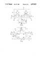
- FIG. 4is a "calma" layout describing a plan view of the voltage controlled variable FET resistor used in the attenuator of the present invention in monolithic form.
- FIG. 5is a graph showing the voltage versus resistance relationships of each of the individual FET segments of a voltage controlled variable FET resistor used in the attenuator of the present invention.
- FIG. 6is a graph showing the resistance versus voltage relationship of a voltage controlled variable FET resistor used in the attenuator of the present invention.
- FIG. 7is a schematic diagram of the attenuator of the present invention in a bridged T configuration.
- FIG. 8is a schematic diagram of the attenuator of the present invention in a T configuration.
- FIG. 9is a schematic diagram of the attenuator of the present invention in a PI configuration.
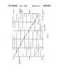
- FIG. 10is a "calma" layout describing a plan view of the bridged T attenuator of the present invention in monolithic form.
- FIG. 11is a graph of the attenuation versus voltage relationship of a bridged T attenuator of the invention.
- variable attenuator of the inventionis shown in a schematic block diagram in FIG. 2 in which the attenuator 1 includes a first branch circuit 2 coupled to a source terminal 3 and a load terminal 4.
- the attenuator 1also includes a second branch circuit 5 coupled to the first branch circuit 2 and a common terminal 6, shown in the illustrative embodiment of FIG. 2 as, ground.
- Each of the first and second branch circuits 2 and 5include a voltage controlled variable FET resistor 10.
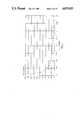
- FIG. 3shows a schematic circuit diagram of the voltage variable FET resistor 10 of the invention comprising a FET network 12 coupled to a voltage divider network 14.
- the FET network 12includes an input terminal 16 and an output terminal 18.
- the voltage divider network 14is coupled to a voltage control terminal 20 and to a ground terminal 22.
- the FET network 12comprises a plurality of FET segments 24 having source (S), drain (D) and gate (G) electrodes.
- the FET segments 24are designated Q 1 , Q 2 , Q 3 . . . Q n and have source, drain and gate electrode designed S 1 , S 2 , S 3 . . . S n ; D 1 , D 2 , D 3 . . . D n ; and G 1 , G 2 , G 3 . . . G n , respectively.
- the number, n, of FET segments in the FET network 12is determined in accordance with the particular application and desired voltage-resistance relationship of the FET resistor 10.
- Each of the FET segments 24 in the FET network 12are coupled in parallel across their respective source and drain electrodes. Accordingly, all the source electrodes S 1 , S 2 , S 3 . . . S n are coupled together to output terminal 18, and all the drain electrodes D 1 , D 2 , D 3 . . . D n are coupled together to input terminal 16.
- the voltage divider network 14includes a plurality of fixed resistors 26 coupled to the gate electrodes of the FET segments 24 between control terminal 20 and ground terminal 22.
- the gate electrodes G 1 , G 2 , G 3 . . . G nare coupled to the voltage divider network 14 at nodes N 1 , N 2 , N 3 . . . N n .
- Resistor R1 of the plurality resistors 26is coupled between node N 1 and N 2 .
- resistor R2is coupled between nodes N 2 and N 3 and resistor R 3 is connected between nodes N 3 and N 4 .
- Resistor R nis connected between node N n and ground terminal 22.
- a field effect transistor operating in the linear range of its I-V characteristic curveacts as a voltage controlled variable resistor.
- the resistance measured between the source and drain electrodesvaries in accordance with the voltage applied to the gate of the transistor.
- the range of resistance valuesis dependent upon manufacturing parameters and in particular, the width of the gate of the FET.
- Each of the FET segments 24 in the network 12have a predetermined gate width resulting in a predetermined channel resistance measured between the source and drain of each FET segment.
- the FET network 12includes at least two or more FET segments 24 in which the gate width of at least one of the FET segments 24 is different from the gate width of at least one other of the FET segments 24.
- the FET segments 24,are connected in parallel and therefore the resistance of the FET resistor 10 measured between terminals 16 and 18 is the equivalent resistance of the FET segments determined by the parallel resistance formula: ##EQU2##
- a control voltage V G applied to the control terminal 20will be divided by the voltage divider network 14 to provide a different voltage to each of the gates of the FET segments 24.
- the individual gate voltagesare designated V 1 , V 2 , V 3 . . . V n , where V 1 equals V G .
- each FET segment 24will have a different relationship between V G and the resistance measured between the source and drain of each FET segment 24. Since the source and drain terminals of each of the FET segments 24 are connected in parallel, the resulting resistance of the complete voltage variable FET resistor 10 can be made to match a specified relationship by changing the number of FET segments 24, the width of each of the FET segments 24 and the voltage divider network 14 resistance values.
- the voltage variable FET resistor 10is shown in monolithic form.
- the plurality of FET segments 24are formed on a semiconducting substrate, such as GaAs from electrodes having an interdigitated construction.
- the FET segment Q 1is shown with a gate width 2W 1 .
- FET segment Q 1is a split FET which is made of two segments F 1 and F 2 coupled to the same metal strip thus connecting the two segments in parallel
- the effective gate width of FET segment Q 1is equal to the gate width of segment F 1 plus the gate width of segment F 2 .
- FET segment Q 2 and Q 3have a gate width of W 2 and FET segment Q 4 has a gate width W 4 .
- Resistors R 1 , R 2 , R 3 and R 4are connected as shown to the gates of FET segments Q 1 -Q 4 , between control terminal contact pad 20 and ground terminal contact pad 22.
- the drain electrodes of the FET segments Q 1 -Q 4are connected to input contact pad 16 and the source electrodes of the FET segments Q 1 -Q 4 are connected to output terminal contact pad 18.
- the desired voltage-resistance relationship necessary for a particular applicationis first determined.
- the desired relationshipmay be based on the need to have the resistance between the input and output terminals of the FET resistor 10 vary in a particular manner upon the application and change of the control voltage V G .
- the desired relationshipmay be based on the need to have the resistance between the input and output terminals of the FET resistor 10 vary in a particular manner upon the application and change of the control voltage V G .
- a computer simulation programmay be used to simulate the resistance-voltage relationship of FET resistor 10 for various combinations of gate widths and fixed resistor values to assist in ascertaining the optimal combination.
- FIG. 5is a graph showing the relationships between voltage and channel resistance for each of the individual FET segments Q 1 -Q 4 .
- the resistance for each FET segmentvaries in accordance with each of the plots shown.
- the size of the gate widthaffects the channel resistance in a manner such that a larger width will produce a smaller resistance.
- a smaller parallel resistancewill have a larger contribution to the equivalent resistance.
- the resistors of the voltage divider 14determine when each FET segment will reach pinch off state. Once a FET segment reaches pinch off, the resistance becomes very large and no longer contributes to the equivalent resistance. As shown in FIG.
- FIG. 6is a graph showing the equivalent resistance of the complete FET resistor 10 as a function of the control voltage.
- the relationship between the resistance measured between the output and input terminals and the control voltagemay be determined by varying the number of FET segments, the gate widths of the FET segments and the gate voltages applied to the FET segments.
- variable attenuator of the inventionpermits the variable attenuator of the invention to have almost any chosen relationship between the attenuation and the control voltage.
- a signal with amplitude V Sis applied to source terminal 3.
- the attenuator 1decreases the signal's amplitude and the signal will emerge from the load terminal 4 with an amplitude V L .
- the ratio V S /V Lis the attenuation ratio.
- the control voltages V G1 and V G2change the resistances of the FET resistors 10 and thus control the attenuation ratio and the input and output impedances of the attenuator.
- the input and output impedancesmust be matched for the attenuator to operate properly within the device in which the attenuator is employed.
- variable attenuator of the inventionmay be configured in any topology, such as T, PI or bridged T.
- the relationship between the attenuation ratio and the control voltages V G1 and V G2 applied to the FET resistors 10is directly related to the relationship between the resistance of the FET resistors and the control voltages.
- the network equations for the T, PI and bridged T configurationsare well known to any one skilled in the art. By these equations it is known that the attenuation is a function of the resistor values of the attenuator. Since the resistor value of the FET resistors 10 is a function of the control voltage, it follows that the attenuation is also a function of the control voltage. To achieve a desired relationship between the attenuation and the control voltage, the desired relationship between the channel resistance of FET resistors 10 and the control voltage is determined.
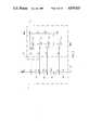
- FIGS. 7, 8 and 9are schematic diagrams of the variable attenuator of the invention implemented in the bridged T, T and PI topologies, respectively.
- FIG. 7shows a bridged T attenuator 30 in which the first branch circuit 2 includes a first voltage variable FET resistor 10, designated Z 1 and two balancing resistors 32 and 34. The two balancing resistors are connected in series between the source and load terminals 3,4. In order to have a reciprocal attenuator, the resistors 32 and 34 must be of equal value.
- the input terminal 36 of the first FET resistor Z 1is coupled to the source terminal 3 and the output terminal 38 of the first FET resistor, Z 1 is coupled to the load terminal 4.
- the second branch circuit 5includes a second voltage variable FET resistor 10, designated Z 2 , having an input terminal 40 coupled to a node 42 between the two balancing resistors 32, 34 and an output terminal 44 coupled to the common terminal 6.
- the variable attenuator 50 of FIG. 8is shown in a T configuration wherein the first branch circuit 2 includes first and second voltage variable FET resistors 10, designated Z 1 and Z 2 coupled in series between the source and load terminals 3,4.
- the input terminal 52 of the first FET resistor Z 1is connected to the source terminal 3.
- the output terminal 54 of the first FET resistor Z 1 and input terminal 56 of the second FET resistor Z 2are connected together at a node 58.
- the output terminal 60 of the second FET resistor Z 2is coupled to the load terminal 4.
- the second branch circuit 5includes a third voltage variable FET resistor 10, designated Z 3 having an input terminal 62 coupled to the node 58 and an output terminal 64 coupled to the common terminal 6.
- the variable attenuator 70 of FIG. 9is configured in a PI topology wherein the first branch circuit 2 includes a first voltage variable FET resistor 10, designated Z 1 having an input terminal 72 coupled to the source terminal 3 and an output terminal 74 coupled to the load terminal 4.
- the second branch circuit 5includes second and third voltage variable FET resistors 10, designated Z 2 and Z 3 , coupled in parallel.
- the input terminal 76 of the second FET resistor Z 2is coupled to the source terminal 3 and the input terminal 78 of the third FET resistor Z 3 is coupled to the load terminal 4.
- the output terminals 80 and 82 of the second and third FET resistors Z 2 and Z 3are both coupled to the common terminal 6.
- an electrical signal of amplitude V Sis entered upon the input 3 of each of the attenuators of FIGS. 7, 8 and 9.
- the attenuatorsdecrease the signal's amplitude and the signal emerging from load terminal 4 has an amplitude V L .
- the attenuation ratio V L /V Sdetermines the attenuation in db.
- the attenuation in dbis equal to 20 log V L /V S .
- a 20 db attenuationprovides for an output signal V L that is 10 percent of the input V S .
- a 40 db attenuationprovides an input signal one percent of V S and a 60 db attenuation provides an output signal 0.1 percent of V S
- the control signal V G1is adjusted to change the attenuation while the control signal V G2 is adjusted to maintain a match of the input impedance Z S and the output impedance Z L to the system's characteristic impedance.
- the adjustmentsare made using the known attenuator network equations and the equations governing the resistance of the voltage variable FETs 10.
- the bridged T configuration attenuator 30is provided with a linear relationship between V G1 and the attenuation ratio, while keeping matched impedances on both the input and output.
- the attenuator 30is shown in FIG. 10 implemented in monolithic form.
- the voltage controlled variable FET Z 1 of bridged T attenuator 30is identical to the monolithic FET resistor shown in FIG. 4.
- the second voltage controlled FET resistor Z 2is shown as having two FET segments Q5 and Q6 each having a gate width of W 5 of 125 microns.
- the resistors for the voltage divider network of the FET resistor Z 2are shown as R 5 and R 6 .
- the balancing resistors 32 and 34are as indicated.
- R 5is equal to 1k ohms and R 6 is equal to 2.8k ohms.
- V G1adjusted from 0.0 volts to -5.0 volts
- a linear attenuationresults as shown in FIG. 11.
- the attenuationvaried linearly from 2 db to 15 db.
- the return lossis also shown in the graph of FIG. 11.
- the return lossis a measure of the impedance mismatch by measuring the power reflected back to the input.
- the return loss as shown in FIG. 11is well within the acceptable range for attenuators. Attached to the application as Appendix A is a copy of a computer simulation program for the bridged T attenuator of FIGS. 7 and 10.
- the voltage variable attenuators of the inventionare particularly useful in the microwave frequency range, but may also be used in low frequency ranges.
- the MMIC voltage variable attenuator of the inventionfeatures over a 10 db attenuation range, within the DC to 12 GHz frequency band where the attenuation varies linearly with the control voltage.
- the linearity of the attenuatorsmakes them particularly appealing for applications such as temperature gain compensation of GaAs FET amplifiers.
Landscapes
- Networks Using Active Elements (AREA)
Abstract
Description
TABLE ______________________________________ RESISTANCE GATE WIDTHS ______________________________________ R.sub.1 = 4.5 k ohms W.sub.1 = 110 microns (2 × 55) R.sub.2 = 1.9 k ohms W.sub.2 = 40 microns R.sub.3 = 1.7 k ohms W.sub.3 = 40 microns R.sub.4 = 1.6 k ohms W.sub.4 = 35 microns ______________________________________
Claims (31)
Priority Applications (3)
| Application Number | Priority Date | Filing Date | Title |
|---|---|---|---|
| US07/192,193US4875023A (en) | 1988-05-10 | 1988-05-10 | Variable attenuator having voltage variable FET resistor with chosen resistance-voltage relationship |
| CA000599151ACA1300221C (en) | 1988-05-10 | 1989-05-09 | Variable attenuator having voltage variable fet resistor with chosen resistance-voltage relationship |
| PCT/US1989/002019WO1989011166A1 (en) | 1988-05-10 | 1989-05-10 | Variable attenuator having voltage variable fet resistor with chosen resistance-voltage relationship |
Applications Claiming Priority (1)
| Application Number | Priority Date | Filing Date | Title |
|---|---|---|---|
| US07/192,193US4875023A (en) | 1988-05-10 | 1988-05-10 | Variable attenuator having voltage variable FET resistor with chosen resistance-voltage relationship |
Publications (1)
| Publication Number | Publication Date |
|---|---|
| US4875023Atrue US4875023A (en) | 1989-10-17 |
Family
ID=22708634
Family Applications (1)
| Application Number | Title | Priority Date | Filing Date |
|---|---|---|---|
| US07/192,193Expired - Fee RelatedUS4875023A (en) | 1988-05-10 | 1988-05-10 | Variable attenuator having voltage variable FET resistor with chosen resistance-voltage relationship |
Country Status (3)
| Country | Link |
|---|---|
| US (1) | US4875023A (en) |
| CA (1) | CA1300221C (en) |
| WO (1) | WO1989011166A1 (en) |
Cited By (23)
| Publication number | Priority date | Publication date | Assignee | Title |
|---|---|---|---|---|
| US4996504A (en)* | 1988-09-30 | 1991-02-26 | Siemens Aktiengesellschaft | Monolithically integratable microwave attenuation element |
| US5001524A (en)* | 1989-06-05 | 1991-03-19 | Motorola, Inc. | Digitally controlled field effect attenuator devices |
| US5049841A (en)* | 1990-07-11 | 1991-09-17 | General Electric Company | Electronically reconfigurable digital pad attenuator using segmented field effect transistors |
| US5087899A (en)* | 1988-05-19 | 1992-02-11 | Siemens-Albis Ag | Variable attenuation network with constant input and output resistances |
| US5191338A (en)* | 1991-11-29 | 1993-03-02 | General Electric Company | Wideband transmission-mode FET linearizer |
| US5298817A (en)* | 1993-02-09 | 1994-03-29 | At&T Bell Laboratories | High-frequency solid-state relay |
| US5648740A (en)* | 1994-11-03 | 1997-07-15 | Gec-Marconi Limited | Switching arrangement with combined attenuation and selection stage |
| EP0696845A3 (en)* | 1994-08-08 | 1998-04-01 | Oki Electric Industry Co., Ltd. | Variable resistor and gain control circuit and integrated circuit having the variable resistor |
| US5786739A (en)* | 1996-09-03 | 1998-07-28 | Hughes Electronics | Integrated evanescent mode filter with adjustable attenuator |
| US6281740B1 (en)* | 1994-03-23 | 2001-08-28 | Telefonaktiebolaget Lm Ericsson | Connecting arrangement for selectively presenting resistive properties using transistors |
| US20030206025A1 (en)* | 2000-07-14 | 2003-11-06 | Volterra Semiconductor Corporation, A Delaware Corporation | Testing integrated circuits and integrated power transistors |
| US20040247327A1 (en)* | 2003-06-06 | 2004-12-09 | Walid Kamali | Optical receiver having an open loop automatic gain control circuit |
| JP2006295594A (en)* | 2005-04-12 | 2006-10-26 | Matsushita Electric Ind Co Ltd | Transistor circuit |
| US20070072569A1 (en)* | 2005-09-28 | 2007-03-29 | Mccarthy Daniel P | Linear voltage controlled variable attenuator with linear DB/V gain slope |
| US20090027822A1 (en)* | 2007-07-26 | 2009-01-29 | Darwish Mohamed N | Transient blocking unit having a fab-adjustable threshold current |
| US20090284311A1 (en)* | 2005-06-07 | 2009-11-19 | Sony Corporation | Resistor circuit |
| CN103066947A (en)* | 2012-12-29 | 2013-04-24 | 南京理工大学 | Ultra wide band large dynamic figure / analog compatible adjustable attenuator |
| US8890598B2 (en) | 2013-01-25 | 2014-11-18 | Analog Devices, Inc. | Multiple ramp variable attenuator |
| US9590591B1 (en) | 2016-03-17 | 2017-03-07 | Analog Devices Global | High frequency signal attenuators |
| US9882549B2 (en) | 2016-02-23 | 2018-01-30 | Analog Devices Global | Apparatus and methods for high linearity voltage variable attenuators |
| US10103712B2 (en) | 2016-12-15 | 2018-10-16 | Analog Devices Global | Voltage variable attenuator, an integrated circuit and a method of attenuation |
| US11209802B2 (en)* | 2018-04-23 | 2021-12-28 | Rockwell Automation Technologies, Inc. | Industrial control module providing universal I/O |
| US12394303B1 (en) | 2024-03-22 | 2025-08-19 | Waterford Consultants, LLC | Systems for mitigating radio-frequency radiation exposure using power interrupters |
Families Citing this family (3)
| Publication number | Priority date | Publication date | Assignee | Title |
|---|---|---|---|---|
| US4967169A (en)* | 1989-07-31 | 1990-10-30 | Teledyne Mec | FET monolithic microwave integrated circuit variable slope gain-equalizer |
| JP3362931B2 (en)* | 1993-09-30 | 2003-01-07 | ソニー株式会社 | Attenuator circuit |
| US10651825B2 (en) | 2018-04-03 | 2020-05-12 | Mediatek Singapore Pte. Ltd. | Resistor-based attenuator systems |
Citations (36)
| Publication number | Priority date | Publication date | Assignee | Title |
|---|---|---|---|---|
| US3598908A (en)* | 1968-08-30 | 1971-08-10 | Ampex | Digitally controlled lap dissolver |
| US3968452A (en)* | 1973-11-13 | 1976-07-06 | Sony Corporation | Signal level control circuit |
| US3977291A (en)* | 1974-08-13 | 1976-08-31 | C. G. Conn, Ltd. | Attenuator network for musical instrument keying system |
| US4004164A (en)* | 1975-12-18 | 1977-01-18 | International Business Machines Corporation | Compensating current source |
| US4016481A (en)* | 1975-11-26 | 1977-04-05 | Gte Automatic Electric Laboratories Incorporated | Unmatched field effect transistors providing matched voltage-controlled resistances |
| US4039981A (en)* | 1975-04-04 | 1977-08-02 | Hitachi, Ltd. | Variable impedance circuit |
| US4088943A (en)* | 1977-02-25 | 1978-05-09 | Electro-Craft Corporation | Brushless DC tachometer circuit |
| US4090139A (en)* | 1976-05-07 | 1978-05-16 | Rca Corporation | Complementary symmetry FET mixer circuits |
| US4093909A (en)* | 1976-07-21 | 1978-06-06 | General Electric Company | Method and apparatus for operating a semiconductor integrated circuit at minimum power requirements |
| US4121183A (en)* | 1976-10-29 | 1978-10-17 | Tektronix, Inc. | Programmable attenuator apparatus employing active FET switching |
| US4202238A (en)* | 1978-06-01 | 1980-05-13 | Norlin Industries, Inc. | Compressor-expander for a musical instrument |
| US4241316A (en)* | 1979-01-18 | 1980-12-23 | Lawrence Kavanau | Field effect transconductance amplifiers |
| US4244043A (en)* | 1978-03-31 | 1981-01-06 | Citizen Watch Co., Ltd. | Frequency division system |
| US4255716A (en)* | 1977-09-10 | 1981-03-10 | Tokyo Shibaura Denki Kabushiki Kaisha | Automatic gain control circuit |
| US4257064A (en)* | 1980-02-19 | 1981-03-17 | Hughes Aircraft Company | Wideband linear video contrast control |
| US4317055A (en)* | 1978-05-24 | 1982-02-23 | Hitachi, Ltd. | High-voltage circuit for insulated gate field-effect transistor |
| US4375596A (en)* | 1979-11-19 | 1983-03-01 | Nippon Electric Co., Ltd. | Reference voltage generator circuit |
| US4395643A (en)* | 1979-12-15 | 1983-07-26 | Robert Bosch Gmbh | Broadband circuit with rapidly variable resistor |
| US4425515A (en)* | 1981-11-16 | 1984-01-10 | Hewlett-Packard Company | Method and means to minimize risetime of a microwave pulse modulated signal from a frequency multiplier circuit |
| US4546651A (en)* | 1984-04-02 | 1985-10-15 | Hewlett-Packard Co. | Transducer coupling |
| US4549098A (en)* | 1981-09-09 | 1985-10-22 | Nippon Gakki Seizo Kabushiki Kaisha | Device for generating a variable control signal |
| US4549197A (en)* | 1982-07-06 | 1985-10-22 | Texas Instruments Incorporated | Common-gate GaAs FET design for monolithic microwave integrated circuits |
| US4555788A (en)* | 1984-02-23 | 1985-11-26 | Itt Corporation | Multiple rate baseband receiver |
| US4562362A (en)* | 1982-10-18 | 1985-12-31 | Tektronix, Inc. | Automatic trigger sensitivity adjustment circuit |
| US4605912A (en)* | 1981-12-03 | 1986-08-12 | General Electric Company | Continuously variable phase shifting element comprised of interdigitated electrode MESFET |
| US4638190A (en)* | 1985-05-20 | 1987-01-20 | General Electric Company | Digitally controlled wideband phase shifter |
| US4646028A (en)* | 1984-08-27 | 1987-02-24 | Texas Instruments Incorporated | GaAs monolithic medium power amplifier |
| US4649291A (en)* | 1983-05-26 | 1987-03-10 | Kabushiki Kaisha Toshiba | Voltage reference circuit for providing a predetermined voltage to an active element circuit |
| US4663584A (en)* | 1985-06-10 | 1987-05-05 | Kabushiki Kaisha Toshiba | Intermediate potential generation circuit |
| JPS62122313A (en)* | 1985-11-22 | 1987-06-03 | Hitachi Ltd | FET VCR distortion compensation circuit |
| US4686451A (en)* | 1986-10-15 | 1987-08-11 | Triquint Semiconductor, Inc. | GaAs voltage reference generator |
| US4686387A (en)* | 1984-01-20 | 1987-08-11 | Thomson-Csf | Biasing circuit for a field effect transistor |
| US4688113A (en)* | 1985-10-01 | 1987-08-18 | Telex Computer Products, Inc. | Apparatus for calibrating tape drive read system |
| US4700462A (en)* | 1986-10-08 | 1987-10-20 | Hughes Aircraft Company | Process for making a T-gated transistor |
| US4701722A (en)* | 1985-06-17 | 1987-10-20 | Dolby Ray Milton | Circuit arrangements for modifying dynamic range using series and parallel circuit techniques |
| US4719434A (en)* | 1981-08-14 | 1988-01-12 | Texas Instruments Incorporated | Varactor trimming for MMICs |
- 1988
- 1988-05-10USUS07/192,193patent/US4875023A/ennot_activeExpired - Fee Related
- 1989
- 1989-05-09CACA000599151Apatent/CA1300221C/ennot_activeExpired - Lifetime
- 1989-05-10WOPCT/US1989/002019patent/WO1989011166A1/enunknown
Patent Citations (38)
| Publication number | Priority date | Publication date | Assignee | Title |
|---|---|---|---|---|
| US3598908A (en)* | 1968-08-30 | 1971-08-10 | Ampex | Digitally controlled lap dissolver |
| US3968452A (en)* | 1973-11-13 | 1976-07-06 | Sony Corporation | Signal level control circuit |
| US3977291A (en)* | 1974-08-13 | 1976-08-31 | C. G. Conn, Ltd. | Attenuator network for musical instrument keying system |
| US4039981A (en)* | 1975-04-04 | 1977-08-02 | Hitachi, Ltd. | Variable impedance circuit |
| US4016481A (en)* | 1975-11-26 | 1977-04-05 | Gte Automatic Electric Laboratories Incorporated | Unmatched field effect transistors providing matched voltage-controlled resistances |
| US4004164A (en)* | 1975-12-18 | 1977-01-18 | International Business Machines Corporation | Compensating current source |
| US4090139A (en)* | 1976-05-07 | 1978-05-16 | Rca Corporation | Complementary symmetry FET mixer circuits |
| US4093909A (en)* | 1976-07-21 | 1978-06-06 | General Electric Company | Method and apparatus for operating a semiconductor integrated circuit at minimum power requirements |
| US4121183A (en)* | 1976-10-29 | 1978-10-17 | Tektronix, Inc. | Programmable attenuator apparatus employing active FET switching |
| US4088943A (en)* | 1977-02-25 | 1978-05-09 | Electro-Craft Corporation | Brushless DC tachometer circuit |
| US4255716A (en)* | 1977-09-10 | 1981-03-10 | Tokyo Shibaura Denki Kabushiki Kaisha | Automatic gain control circuit |
| US4244043A (en)* | 1978-03-31 | 1981-01-06 | Citizen Watch Co., Ltd. | Frequency division system |
| US4317055A (en)* | 1978-05-24 | 1982-02-23 | Hitachi, Ltd. | High-voltage circuit for insulated gate field-effect transistor |
| US4202238A (en)* | 1978-06-01 | 1980-05-13 | Norlin Industries, Inc. | Compressor-expander for a musical instrument |
| US4241316A (en)* | 1979-01-18 | 1980-12-23 | Lawrence Kavanau | Field effect transconductance amplifiers |
| US4496909A (en)* | 1979-01-18 | 1985-01-29 | Lawrence Kavanau | Biasing method for improved performance in field effect devices |
| US4375596A (en)* | 1979-11-19 | 1983-03-01 | Nippon Electric Co., Ltd. | Reference voltage generator circuit |
| US4395643A (en)* | 1979-12-15 | 1983-07-26 | Robert Bosch Gmbh | Broadband circuit with rapidly variable resistor |
| US4257064A (en)* | 1980-02-19 | 1981-03-17 | Hughes Aircraft Company | Wideband linear video contrast control |
| US4719434A (en)* | 1981-08-14 | 1988-01-12 | Texas Instruments Incorporated | Varactor trimming for MMICs |
| US4549098A (en)* | 1981-09-09 | 1985-10-22 | Nippon Gakki Seizo Kabushiki Kaisha | Device for generating a variable control signal |
| US4425515A (en)* | 1981-11-16 | 1984-01-10 | Hewlett-Packard Company | Method and means to minimize risetime of a microwave pulse modulated signal from a frequency multiplier circuit |
| US4605912A (en)* | 1981-12-03 | 1986-08-12 | General Electric Company | Continuously variable phase shifting element comprised of interdigitated electrode MESFET |
| US4549197A (en)* | 1982-07-06 | 1985-10-22 | Texas Instruments Incorporated | Common-gate GaAs FET design for monolithic microwave integrated circuits |
| US4562362A (en)* | 1982-10-18 | 1985-12-31 | Tektronix, Inc. | Automatic trigger sensitivity adjustment circuit |
| US4649291A (en)* | 1983-05-26 | 1987-03-10 | Kabushiki Kaisha Toshiba | Voltage reference circuit for providing a predetermined voltage to an active element circuit |
| US4686387A (en)* | 1984-01-20 | 1987-08-11 | Thomson-Csf | Biasing circuit for a field effect transistor |
| US4555788A (en)* | 1984-02-23 | 1985-11-26 | Itt Corporation | Multiple rate baseband receiver |
| US4546651A (en)* | 1984-04-02 | 1985-10-15 | Hewlett-Packard Co. | Transducer coupling |
| US4646028A (en)* | 1984-08-27 | 1987-02-24 | Texas Instruments Incorporated | GaAs monolithic medium power amplifier |
| US4638190A (en)* | 1985-05-20 | 1987-01-20 | General Electric Company | Digitally controlled wideband phase shifter |
| US4663584A (en)* | 1985-06-10 | 1987-05-05 | Kabushiki Kaisha Toshiba | Intermediate potential generation circuit |
| US4663584B1 (en)* | 1985-06-10 | 1996-05-21 | Toshiba Kk | Intermediate potential generation circuit |
| US4701722A (en)* | 1985-06-17 | 1987-10-20 | Dolby Ray Milton | Circuit arrangements for modifying dynamic range using series and parallel circuit techniques |
| US4688113A (en)* | 1985-10-01 | 1987-08-18 | Telex Computer Products, Inc. | Apparatus for calibrating tape drive read system |
| JPS62122313A (en)* | 1985-11-22 | 1987-06-03 | Hitachi Ltd | FET VCR distortion compensation circuit |
| US4700462A (en)* | 1986-10-08 | 1987-10-20 | Hughes Aircraft Company | Process for making a T-gated transistor |
| US4686451A (en)* | 1986-10-15 | 1987-08-11 | Triquint Semiconductor, Inc. | GaAs voltage reference generator |
Non-Patent Citations (3)
| Title |
|---|
| Fisher, D. et al., A Linear GaAs MMIC Variable Attenuator, RF Design, Oct. 1987.* |
| Lizama, G. et al., 1 6 GHz GaAs MMIC Linear Attenuator with Integral Drivers, IEEE 1987 Microwave and Millimeter Wave Monolithic Circuits Symposium, 1987.* |
| Lizama, G. et al., 1-6 GHz GaAs MMIC Linear Attenuator with Integral Drivers, IEEE 1987 Microwave and Millimeter-Wave Monolithic Circuits Symposium, 1987. |
Cited By (29)
| Publication number | Priority date | Publication date | Assignee | Title |
|---|---|---|---|---|
| US5087899A (en)* | 1988-05-19 | 1992-02-11 | Siemens-Albis Ag | Variable attenuation network with constant input and output resistances |
| US4996504A (en)* | 1988-09-30 | 1991-02-26 | Siemens Aktiengesellschaft | Monolithically integratable microwave attenuation element |
| US5001524A (en)* | 1989-06-05 | 1991-03-19 | Motorola, Inc. | Digitally controlled field effect attenuator devices |
| US5049841A (en)* | 1990-07-11 | 1991-09-17 | General Electric Company | Electronically reconfigurable digital pad attenuator using segmented field effect transistors |
| US5191338A (en)* | 1991-11-29 | 1993-03-02 | General Electric Company | Wideband transmission-mode FET linearizer |
| US5298817A (en)* | 1993-02-09 | 1994-03-29 | At&T Bell Laboratories | High-frequency solid-state relay |
| US6281740B1 (en)* | 1994-03-23 | 2001-08-28 | Telefonaktiebolaget Lm Ericsson | Connecting arrangement for selectively presenting resistive properties using transistors |
| EP0696845A3 (en)* | 1994-08-08 | 1998-04-01 | Oki Electric Industry Co., Ltd. | Variable resistor and gain control circuit and integrated circuit having the variable resistor |
| US5648740A (en)* | 1994-11-03 | 1997-07-15 | Gec-Marconi Limited | Switching arrangement with combined attenuation and selection stage |
| US5786739A (en)* | 1996-09-03 | 1998-07-28 | Hughes Electronics | Integrated evanescent mode filter with adjustable attenuator |
| US20030206025A1 (en)* | 2000-07-14 | 2003-11-06 | Volterra Semiconductor Corporation, A Delaware Corporation | Testing integrated circuits and integrated power transistors |
| US6759856B2 (en)* | 2000-07-14 | 2004-07-06 | Volterra Semiconductor, Inc. | Testing integrated circuits and integrated power transistors |
| US20040247327A1 (en)* | 2003-06-06 | 2004-12-09 | Walid Kamali | Optical receiver having an open loop automatic gain control circuit |
| US7599629B2 (en)* | 2003-06-06 | 2009-10-06 | Scientific-Atlanta, Inc. | Optical receiver having an open loop automatic gain control circuit |
| JP2006295594A (en)* | 2005-04-12 | 2006-10-26 | Matsushita Electric Ind Co Ltd | Transistor circuit |
| US7659765B2 (en)* | 2005-06-07 | 2010-02-09 | Sony Corporation | Resistor circuit |
| US20090284311A1 (en)* | 2005-06-07 | 2009-11-19 | Sony Corporation | Resistor circuit |
| US20070072569A1 (en)* | 2005-09-28 | 2007-03-29 | Mccarthy Daniel P | Linear voltage controlled variable attenuator with linear DB/V gain slope |
| US7505748B2 (en)* | 2005-09-28 | 2009-03-17 | Freescale Semicondductor, Inc. | Linear voltage controlled variable attenuator with linear DB/V gain slope |
| US8131241B2 (en) | 2005-09-28 | 2012-03-06 | Freescale Semiconductor, Inc. | Linear voltage controlled variable attenuator with linear DB/V gain slope |
| US20090027822A1 (en)* | 2007-07-26 | 2009-01-29 | Darwish Mohamed N | Transient blocking unit having a fab-adjustable threshold current |
| CN103066947A (en)* | 2012-12-29 | 2013-04-24 | 南京理工大学 | Ultra wide band large dynamic figure / analog compatible adjustable attenuator |
| US8890598B2 (en) | 2013-01-25 | 2014-11-18 | Analog Devices, Inc. | Multiple ramp variable attenuator |
| US9882549B2 (en) | 2016-02-23 | 2018-01-30 | Analog Devices Global | Apparatus and methods for high linearity voltage variable attenuators |
| US9590591B1 (en) | 2016-03-17 | 2017-03-07 | Analog Devices Global | High frequency signal attenuators |
| TWI631762B (en)* | 2016-03-17 | 2018-08-01 | 亞德諾半導體環球公司 | High frequency signal attenuator |
| US10103712B2 (en) | 2016-12-15 | 2018-10-16 | Analog Devices Global | Voltage variable attenuator, an integrated circuit and a method of attenuation |
| US11209802B2 (en)* | 2018-04-23 | 2021-12-28 | Rockwell Automation Technologies, Inc. | Industrial control module providing universal I/O |
| US12394303B1 (en) | 2024-03-22 | 2025-08-19 | Waterford Consultants, LLC | Systems for mitigating radio-frequency radiation exposure using power interrupters |
Also Published As
| Publication number | Publication date |
|---|---|
| CA1300221C (en) | 1992-05-05 |
| WO1989011166A1 (en) | 1989-11-16 |
Similar Documents
| Publication | Publication Date | Title |
|---|---|---|
| US4875023A (en) | Variable attenuator having voltage variable FET resistor with chosen resistance-voltage relationship | |
| US4864162A (en) | Voltage variable FET resistor with chosen resistance-voltage relationship | |
| US4975604A (en) | Automatic return-loss optimization of a variable fet attenuator | |
| US5049841A (en) | Electronically reconfigurable digital pad attenuator using segmented field effect transistors | |
| US5361038A (en) | Active load applications for distributed circuits | |
| US5633610A (en) | Monolithic microwave integrated circuit apparatus | |
| US5448207A (en) | Attenuator circuit apparatus | |
| US5208547A (en) | Distributed amplifier having negative feedback | |
| US5912599A (en) | Bandwidth compensated bridged-tee attenuator | |
| US5349312A (en) | Voltage variable attenuator | |
| US5309048A (en) | Distributed digital attenuator | |
| US5726613A (en) | Active inductor | |
| US4772858A (en) | Distributed amplifying switch/rf combiner | |
| US5461265A (en) | High-frequency variable impedance circuit having improved linearity of operating characteristics | |
| KR100297044B1 (en) | Step attenuator | |
| US5786737A (en) | Impedance matching circuit and thin film measuring prober | |
| JP2643662B2 (en) | High power field effect transistor amplifier | |
| US5949287A (en) | Power amplifier | |
| US5202649A (en) | Microwave integrated circuit device having impedance matching | |
| US4908531A (en) | Monolithic active isolator | |
| JP3284015B2 (en) | Semiconductor integrated circuit | |
| KR100375520B1 (en) | Linearizer | |
| JP2924483B2 (en) | Variable attenuator | |
| JPH0779132A (en) | Variable attenuator | |
| JP2959004B2 (en) | Semiconductor integrated circuit |
Legal Events
| Date | Code | Title | Description |
|---|---|---|---|
| AS | Assignment | Owner name:TACHONICS CORPORATION, 107 MORGAN LANE, PLAINSBORO Free format text:ASSIGNMENT OF ASSIGNORS INTEREST.;ASSIGNOR:MAOZ, BARAK;REEL/FRAME:004892/0977 Effective date:19880501 Owner name:TACHONICS CORPORATION, NEW JERSEY Free format text:ASSIGNMENT OF ASSIGNORS INTEREST;ASSIGNOR:MAOZ, BARAK;REEL/FRAME:004892/0977 Effective date:19880501 | |
| AS | Assignment | Owner name:GRUMMAN AEROSPACE CORPORATION, BETHPAGE, NEW YORK Free format text:ASSIGNMENT OF ASSIGNORS INTEREST.;ASSIGNOR:TACHONICS CORPORATION, A DE CORP.;REEL/FRAME:004962/0742 Effective date:19880921 Owner name:GRUMMAN AEROSPACE CORPORATION, A NEW YORK CORP., N Free format text:ASSIGNMENT OF ASSIGNORS INTEREST;ASSIGNOR:TACHONICS CORPORATION, A DE CORP.;REEL/FRAME:004962/0742 Effective date:19880921 | |
| FEPP | Fee payment procedure | Free format text:PAYOR NUMBER ASSIGNED (ORIGINAL EVENT CODE: ASPN); ENTITY STATUS OF PATENT OWNER: LARGE ENTITY | |
| FEPP | Fee payment procedure | Free format text:PAYOR NUMBER ASSIGNED (ORIGINAL EVENT CODE: ASPN); ENTITY STATUS OF PATENT OWNER: LARGE ENTITY Free format text:PAYER NUMBER DE-ASSIGNED (ORIGINAL EVENT CODE: RMPN); ENTITY STATUS OF PATENT OWNER: LARGE ENTITY | |
| CC | Certificate of correction | ||
| FPAY | Fee payment | Year of fee payment:4 | |
| FEPP | Fee payment procedure | Free format text:PAYER NUMBER DE-ASSIGNED (ORIGINAL EVENT CODE: RMPN); ENTITY STATUS OF PATENT OWNER: LARGE ENTITY Free format text:PAYOR NUMBER ASSIGNED (ORIGINAL EVENT CODE: ASPN); ENTITY STATUS OF PATENT OWNER: LARGE ENTITY | |
| FPAY | Fee payment | Year of fee payment:8 | |
| REMI | Maintenance fee reminder mailed | ||
| LAPS | Lapse for failure to pay maintenance fees | ||
| STCH | Information on status: patent discontinuation | Free format text:PATENT EXPIRED DUE TO NONPAYMENT OF MAINTENANCE FEES UNDER 37 CFR 1.362 | |
| FP | Lapsed due to failure to pay maintenance fee | Effective date:20011017 |