US4868822A - Memory emulation method and system for testing and troubleshooting microprocessor-based electronic systems - Google Patents
Memory emulation method and system for testing and troubleshooting microprocessor-based electronic systemsDownload PDFInfo
- Publication number
- US4868822A US4868822AUS07/158,223US15822388AUS4868822AUS 4868822 AUS4868822 AUS 4868822AUS 15822388 AUS15822388 AUS 15822388AUS 4868822 AUS4868822 AUS 4868822A
- Authority
- US
- United States
- Prior art keywords
- microprocessor
- memory
- bus
- accordance
- instructions
- Prior art date
- Legal status (The legal status is an assumption and is not a legal conclusion. Google has not performed a legal analysis and makes no representation as to the accuracy of the status listed.)
- Expired - Fee Related
Links
Images


Classifications
- G—PHYSICS
- G06—COMPUTING OR CALCULATING; COUNTING
- G06F—ELECTRIC DIGITAL DATA PROCESSING
- G06F11/00—Error detection; Error correction; Monitoring
- G06F11/22—Detection or location of defective computer hardware by testing during standby operation or during idle time, e.g. start-up testing
- G06F11/26—Functional testing
- G06F11/261—Functional testing by simulating additional hardware, e.g. fault simulation
Definitions
- the present inventionrelates generally to testing and troubleshooting microprocessor-based electronic systems, and in particular to testing and troubleshooting such microprocessor-based systems using memory emulation techniques.
- test techniquessuch as signature analysis, logic level detection, frequency and event counting, pulsing and emulative testing, are well known and have been used for many years.
- emulative testersso called because they emulate the behavior of kernel-related devices, are popular for functional testing and fault isolation in microprocessor-based boards or systems because in the first place they test the system from the inside out, and in the second place they can test a system in which the kernel is dead.
- test systemwhich itself is a microprocessor-based system, is connected in place of a microprocessor in a unit under test (UUT).
- UUTunit under test
- the Bhaskar et al. test systemoperates in a bus-access mode wherein single cycles of bus accesses are made and acted upon before making another. That is, for one bus cycle, the test system microprocessor is switched into signal communication with the UUT bus to perform a read or write operation.
- test system microprocessoris switched over to the test system internal circuitry to generate another read or write command with a new address, or deal with information read from the UUT's memory.
- the bus switching required to effect single cycles of bus accessesis becoming a limitation of microprocessor emulators such as that described by Bhaskar et al. as microprocessor-based systems become more complex and operate at higher speeds.
- Suitable bus switches for newer microprocessor-based UUT's, e.g., for 80386 systems,are non-trivial and difficult to design. Accordingly, it would be desirable to provide a different method by which a test system can be connected into the kernel of a UUT to carry out diagnostic test procedures.
- ROMRead-Only Memory
- ROM emulatorshave been used for software development or to verify that hardware is working. ROM emulators historically have not been used for troubleshooting or fault detection because no sync signal is available to synchronize test equipment with test results, and further because test equipment could not directly retrieve test information from the UUT ROM socket. A partial solution to this problem is described in U.S. Pat. No.
- a method and system for testing and troubleshooting microprocessor-based electronic systemsemploys memory emulation techniques in addition to other troubleshooting techniques to provide complete functionality tests and fault location.
- the test systemcomprises a microprocessor-based mainframe and an interface pod also including a microprocessor-based system which is connected to both the microprocessor and memory space of a unit under test (UUT).
- the interface podincludes special logic circuitry connected to the UUT microprocessor to provide a fine resolution sync pulse during a bus cycle of interest in order to provide full troubleshooting fault isolation that is as effective as that provided by prior art microprocessor emulation.
- the interface podgains control of the UUT microprocessor, which then executes instructions provided by emulation RAM connected to the UUT memory space.
- An analyzer RAMmonitors the UUT connections on a bus-cycle-by-bus-cycle basis, and indicates whether faults occur and on which bus cycle.
- the overall systempermits several test features to be effected, including using the address lines of the UUT memory to retrieve diagnostic data, using the UUT chip select line to encode data which is retrieved and analyzed, using the analyzer RAM to facilitate a UUT bus test technique that allows full fault isolation of such faults, and a system of checks and balances to ensure that bus access took place correctly and that the UUT is kept alive while data is being analyzed. Also, the analyzer RAM facilitates a pipeline correction technique to ensure that UUT microprocessors with pipelining or prefetch features operate correctly.
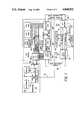
- FIG. 1is a generalized block diagram of a test system in accordance with the present invention
- FIG. 2is a more detailed block diagram of the emulation RAM connection of the interface pod of FIG. 1;
- FIG. 3is a more detailed block diagram of the logic circuit of the interface pod of FIG. 1 and its connection to the UUT microprocessor;
- FIG. 4is a flow chart of a command byte execution program including a standby loop.
- a generalized block diagram of a test system for functionally testing and diagnosing faults in microprocessor-based systems, or units under test (UUTs), in accordance with the present inventionincludes a mainframe 10 electrically connected to an interface pod 12, which in turn is electrically connected to a UUT 14 in a manner to be described in detail later.
- Mainframe 10includes, among other things, a keyboard 20 and a display device 22 electrically connected to a control and measurement circuits block 24.
- the control and measurements circuit blockincludes a microprocessor-based system, and is coupled via a bus 26 to an input/output circuit (I/O) 28 to communicate with the interface pod 12.
- I/Oinput/output circuit
- probe 32Also connected to control and measurement circuits block 24 via a cable 30 is a probe 32, shown physically located for troubleshooting purposes within the UUT 14.
- the mainframecontrols the functional testing and troubleshooting of the UUT in response to actions of an operator, sending instructions and commands to the interface pod, and reporting the results to the operator.
- Examples of commercially-available equipment representative of a mainframe 10are the 9000 Series Micro-System Troubelshooters and 9100 Digital Test Systems manufactured by John Fluke Mfg. Co., Inc.
- Interface pod 12contains a microprocessor-based system which is labeled pod kernel in the drawing.
- the pod kernelis made up of microprocessor 40, ROM 42, RAM 44, and I/O port 46, all of which are interconnected by data, address, and control buses.
- the interface pod 12is connected to the mainframe 10 by a multiple-lead cable 50 coupled between I/O 28 and I/O port 46.
- the pod kernelis connected via its data, address, and control buses to a logic circuit 60, and analyzer RAM 62, and an emulation RAM 64. The purpose of these blocks will be discussed shortly.
- UUT 14is exemplary of any of a wide variety of microprocessor-based systems which may be tested using the system and techniques of the present invention, and only the central or core section will be discussed herein.
- the core sectionincludes a UUT kernel made up of a microprocessor 70 and a memory 72 interconnected by data bus 74 and address bus 76.
- the UUT data and address buses 74 and 76, respectively,are connected to other UUT circuits 78 not germane to this discussion.
- the UUT address busis connected to an address decoder 80 which produces chip select signals on a chip select line 82 connected to the UUT memory 72.
- a multiple-lead cableis connected between logic circuit 60 in the interface pod 12 to the UUT microprocessor 70 to provide communication therebetween.
- UUT memory 72is shown as a dashed line to represent that the UUT memory is either disabled or removed from its socket.
- the cable 92may either plug directly into the UUT memory socket or may be clipped over the pins of a disabled UUT memory.
- the UUT microprocessor 70remains in the circuit and is utilized to execute instructions from the emulation RAM 64.
- UUT microprocessor 70may be a completely different type than the pod microprocessor.
- pod microprocessor 40suitably may be a 68008 while the UUT microprocessor 70 suitably may be a 80386.
- UUt memory 72may be RAM or a ROM, or may be a combination of both.
- a single memoryis provided with a few bytes of ROM space at the higher end of the address space for boot-up purposes while the predominant portion of the memory space is RAM.
- FIG. 1An operator initiates a particular test of interest using the keyboard 20 and display 22, and control measurement circuits 24 generates instructions and commands which are passed through I/O 28, cable 50, and pod I/O 46 to the pod kernel.
- the pod microprocessor 40sets up the circuitry within the interface pod 12 to perform the desired test. Diagnostic instructions are placed in the emulation RAM 64, and reset control is passed through the I/O port 46 and over cable 90 to gain control of microprocessor 70, which resets and then begins executing the instructions in emulation RAM 64.
- Analyzer RAM 62monitors test results coming back over cable 92 and passes these results to the pod kernel which in turn transmits information back to the mainframe 10 via cable 50.
- Cable 90picks timing signals off the microprocessor 70 and returns these to the logic circuit 60, which in turn generates a sync pulse which is returned to the mainframe 10 via cable 50. If faults are detected, the operator may be prompted to place probe 32 on a particular node within the UUT 14, and the sync pulse extracted from the UUT microprocessor 70 ensures that information read by the probe occurs at the appropriate time, i.e., within a bus cycle of interest.
- UUT microprocessor 70is reset, and begins executing instructions presented to memory space 72 by emulation RAM 64.
- UUT address decoder 80decodes the chip selection as a series of ones and zeros.
- the analyzer RAM 62monitors the chip select pin at the memory 72 socket, and indicates faults if a chip select signal during a particular bus cycle is not the logic level expected. In this manner, test results can be passed back to the interface pod from a ROM socket.
- FIG. 2shows in closer detail the interconnection between emulation RAM 64 and UUT memory 72.
- a memory module 100may be provided to condition the signals to ensure proper operation. Of course, if cable 92 is very short, then the memory module 100 is not needed. Included in the memory module 100 are buffers 102 and 104 interposed in the signal paths.
- the end of cable 92may include a connector 110 for connecting directly into a UUT memory socket, and the ROM module 100 may include a socket 112 to plug the UUT memory into.
- an operatorcan select between instructions from the interface pod 12, that is, from emulation RAM 64, or from the UUT memory in socket 112.
- a switch 114may be provided to enable either the data buffer 102 or the memory socket 112 while disabling the other.
- the UUT memory being emulatedis the boot ROM, depending upon the width of the UUT bus, there may be several UUT boot ROMs, requiring several connectors 110 and several memory modules 100.
- the present inventionprovides sufficient flexibility to accommodate almost any UUT memory configuration.
- One important feature of the present inventionis to provide two banks of emulation RAM represented by emulation RAM banks 64A and 64B. To ensure that the UUT remains alive during functional testing, one bank of emulation RAM is always presented to the UUT microprocessor 70 during the test.
- the interface pod 12 pod kernelcan be loading instructions into one of the banks while the other is switched over the UUT memory space and the UUT microprocessor 70 is executing instructions from that other bank.
- the bankscan be switched in such a manner tha UUT microprocessor 70 is unaware that the instructions being executed are coming from another emulation RAM.
- the emulation bank select signalsare produced by logic circuit 60, and will be discussed in connection with FIG. 3.
- Data from the emulation RAM banks 64A and 64Bpasses over a data bus 120 and through buffer 102 to the memory socket.
- Information from the UUT memory socket in the form of UUT memoryinputsis fed back over a bus 122 and through buffer 104 in the memory module 100 to the interface pod 112, and as will be seen later, these UUT memory inputs will be used by the analyzer RAM 62 and by the logic circuit 60.
- a ROM type selection logic circuit 125Also shown in FIG. 2 and connected to the UUT memory inputs bus 122 is a ROM type selection logic circuit 125, which, if UUT memory 72 is a ROM, generates a signal to ensure proper pin information being matched with the interface pod 12. That is, while the physical JEDEC pin configurations may be the same from ROM to ROM, the electrical connections may be different (in other locations) from ROM to ROM.
- the pod kerneltells the logic circuit 126 what type of ROM is to be emulated.
- FIG. 3shows in closer detail logic circuit 60, analyzer RAM 62, and interconnection of logic circuit 60 with the UUT microprocessor 70.
- One important aspect of the present inventionis generating fine-resolution sync pulses at the appropriate time, as mentioned earlier. This is facilitated by picking sync input signals off the UUT microprocessor 70. For example, for the 80386 microprocessor, HOLD, HLDA (Hold Acknowledge), ADS, READY, CLK 2 , and RESET will provide suitable sync input signals. Connections may be made by "flying leads" 140 from a sync module 150, which is connected to cable 90. Sync module 150 contains a suitable sync input buffer 152 to condition the signals to ensure proper operation.
- the cable 90also carries a reset drive control line, which is coupled to the input of a reset drive amplifier 154 in the sync module 150.
- the output of the reset drive amplifier 154is a reset drive signal, which is applied as an override signal to the system reset output of a system reset generator 158 in the UUT 14 to gain control of the UUT mircroprocessor 70.
- Microprocessor signals which might interfere with ability to produce sync signals, such as the HOLD line in the 80386,may be overridden with appropriate control signals.
- the sync module 150is in the circuit because of the long length of cable 92, and may be omitted if the interconnection between logic circuit 60 and UUT microprocessor is sufficiently short.
- Logic circuit 60 in interface pod 12comprises a bus cycle state machine 200, a sync pulse generation state machine 202, an address latch clock state machine 204, an analyzer RAM address generation state machine 206, an emulation RAM bank selection state machine 208, an address comparator 210, and an address latch 212. All of these devices are connected to and receive inputs from the pod kernel control bus. That is, they receive their operational instructions from the pod kernel microprocessor 40 and its associated components.
- Bus cycle state machine 200receives as one of its inputs the sync input signals picked off UUT microprocessor 70, and the other input, as mentioned hereinabove, is a control signal from pod kernel microprocessor 40. Bus cycle state machine 200 monitors the execution of UUT microprocessor 70, and when the bus cycle of interest appears, as determined by the control input from the pod microprocessor 40, it issues control signals to the clock inputs of the other state machines 202-208 in the logic circuit 60.
- Address comparator 210receives as one of its inputs the UUT memory inputs from bus 122 of FIG. 2, and an address or region of addresses supplied by pod microprocessor 40. As the UUT microprocessor executes the instructions supplied by the emulator RAM 64, the address comparator monitors the UUT memory address lines as supplied by bus 122, and when the two inputs match, address comparator 210 "fires" and issues a signal to state machines 205, 206, and 208.
- sync pulse generation for troubleshootingis an important aspect of the present invention, an example of how the sync pulses are generated will be helpful in understanding the basic operation of logic circuit 60.
- An important criterionis that the sync pulse be generated during a bus cycle of interest.
- the interface pod 12is going to command the UUT 14 to perform a Read or a Write operation, and that Read or Write consists of one bus cycle. It is desired for troubleshooting purposes to produce a sync pulse at some selectable time during that Read or Write operation, i.e., address sync pulse, data sync pulse, or some other sync pulse.
- the operatorkeys the bus cycle of interest into the mainframe 10, which in turn commands the interface pod 12 microprocessor 40 to produce a sync pulse at the appropriate time.
- control inputs to bus cycle state machine 200, address latch clock state machine 204, and address comparator 212are loaded with the appropriate control signals.
- the timing of output of sync pulse generation state machine 202is arranged so that an appropriate sync pulse is provided to the mainframe 10 at a time when address information is valid on the UUT microprocessor address bus.
- the appropriate sync pulseis provided to the mainframe when data is valid on the UUT microprocessor data bus.
- Bus cycle state machine 200produces a pulse train in response to the desired sync mode, in response to execution of microprocessor 70 and the control input from microprocessor 40.
- microprocessor 70executes, it continuously fetches instructions of emulator RAM 64, and the addresses of those instructions are monitored by comparator 212.
- address comparator 212"fires,” issuing an output to address latch clock state machine 204, which is simply a synchronizing mechanism to synchronize the comparator output with the UUT microprocessor 70 sync signals.
- the synchronized output of state machine 204is applied to sync pulse generation state machine 202, which starts counting down a preset number of bus cycles, as determined by the control input from the pod kernel, until it issues a sync pulse to the mainframe 10.
- address latch clock state machine 204is also applied to address latch 212, which monitors the UUT memory inputs bus 122 and latches data received therefrom at the appropriate address.
- address latch 212For extracting data over ROM address lines, for example, when the UUT is commanded to perform a Read Bus Cycle, the input to latch 212 may suitably be lower address bits of an address word, while the higher order bits are furnished to the address comparator 210.
- the emulation RAM bank selection state machine 208is simply a flip flop enabled by a control signal from pod microprocessor 40 to select either emulation RAM bank 64A or 64B at the appropriate time as established by address comparator 210 and bus cycle state machine 200.
- the analyzer RAM address generation state machine 206receives inputs from bus cycle state machine 200, address comparator 210, and control inputs from pod microprocessor 40 to produce addresses for analyzer RAM 62 at the appropriate times. Analyzer RAM 62 is utilized to test the integrity of the UUT bus structure.
- Bus testis an important feature use in locating faults on the UUT kernel that cause the UUT microprocessor 70 to behave improperly, or the interface pod 12 to function improperly. For example, if there is short or an open on an address line at the UUT kernel, the UUT microprocessor 70 is not going to be able to fetch instructions properly from the emulator RAM (or from its own memory, for that matter).
- the bus testis perhaps the first step in testing in an unknown UUT, because it ensures that the UUT is at least up and running before going on to the other tests. If fundamental errors exist, then these are noted.
- mainframe 10initializes the bus test, commanding the interface pod 12 to load the bus test program into emulation RAM 64.
- the pod microprocessor 40sets up the analyzer RAM 62 for clocking a sequence of bus cycles into RAM 62, as well as setting up the sync pulse generation state machine 202 to produce sync pulses at appropriate times to troubleshoot a faulty kernel if needed.
- the interface pod microprocessor 40asserts reset of the UUT microprocessor 70, which then begins to execute instructions provided by emulation RAM 64.
- the sequence of UUT bus cyclesis clocked into RAM 62, and when the sequence finishes, the microprocessor 40 evaluates the information stored in RAM 62 to determine if there are any bus faults, and if so, which lines are at fault, and in which step or bus cycle they occurred. The operator can then locate the particular fault using probe 32 in conjunction with sync pulses produced by sync pulse generation state machine 202.
- the operatormay specify the data to be applied to the data bus during first bus cycle after UUT reset.
- the operatormay directly confirm or deny that the data path is valid and operating properly between the memory socket 72 and the UUT microprocessor 70. This measurement technique is necessary to separate data bus direct problems from data bus symptoms indirectly caused other UUT faults.
- the analyzer RAM 62is a dual port device which permits the pod microprocessor 40 to read data out of RAM 62 as well as writing data into it.
- a very flexible troubleshooting mechanismis provided.
- such a systempermits troubleshooting of microprocessors having ⁇ pipeline ⁇ or prefetch features.
- the test system of the present inventioncan determine when pipelining is occurring, and various other factors that occur on the UUT, such as different numbers of "wait" states in a bus cycle which change the sequence that instructions are fetched from the emulation RAM 64. That is, it is desired that the test system understand whether oddities occurring are the result of faults or whether they are simply a function of the pipelining characteristics of the particular microprocessor. And if pipelining is occurring, it is desirable that such pipelining not interfere with the test system's ability to diagnose faults on the UUT kernel.
- the analyzer RAM 62stores addresses and test results.
- a program in the pod kernelanalyzes this information in comparison with expected possibilities, and if a problem exists, the operator is notified via mainframe 10, and appropriate troubleshooting procedures using probe 32 are established. Thus pipelining is recognized and acknowledged by the test system of the present invention, and pass/fail information is passed to the mainframe 10.
- test systemBy way of example in providing a complete understanding of the test system of the present invention, a hypothetical troubleshooting operation will be described. It will be assumed for this example that it is desired to command the UUT microprocessor to execute a "Read" cycle at an address selected by an operator of the test equipment, and to have the results returned to and displayed by the troubleshooting mainframe.
- the test systemis appropriately configured with interface pod 12 connected to mainframe 10, and interface pod 12 connected to the UUT 14.
- Pod microprocessor 40accepts the command and initiates a sequence of events. First, microprocessor 40 examines a status flag in pod RAM 44 to determine if it has control of the UUT, and quickly determines that it does not have control because the emulation RAM 64 does not contain a program. Accordingly, "Read/Write" code written in the machine language for the target UUT microprocessor 70 is loaded from the Pod kernel RAM 44 or ROM 42 into both banks of emulation RAM 64A and 64B.
- pod microprocessorasserts the reset line of UUT microprocessor 70 by applying a reset drive control signal via pod I/O port 46, cable 90, and buffer 154 in sync module 150 to override the output of UUT reset generator 158.
- address comparator 210is set up to monitor a predetermined "communication region" of address space in the emulation RAM 64. Then the reset line of UUT microprocessor 70 is released.
- the communication regionin one proposed commercial embodiment is a 128-byte space, and so seven address lines are used to access this space.
- UUT microprocessor 70begins to fetch instructions ostensibly from its own boot ROM, but actually from the emulation RAM 64 apparently sitting in the UUT memory 72 socket. These first instructions are to initialize the UUT kernel for testing and then to access a predesignated reset-reference address within the communication region of emulsion RAM 64. As soon as this occurs, the address is recognized by address comparator 210, address comparator 210 trips and causes address latch 212 to latch what in this case is the seven lower-order bits of the address in order to determine what is being communicated. This information goes out on the pod kernel data bus to notify the pod microprocessor 40 whether or not the UUT microprocessor 70 has indeed been reset. Thus the interface pod software may use address bits to determine the status of the UUT microprocessor 70 as well as the data that is being returned from a Read operation.
- control of the UUT microprocessor 70is facilitated by the use of two banks of emulation RAM 64.
- address comparator 210may be loaded to monitor the 128-byte communication region of emulation RAM 64 to make sure the UUT microprocessor 70 is not accessing any of those addresses.
- the program loaded into the emulation RAM 64includes instruction which cause the UUT microprocessor 70 to access predesignated addresses within the 128-byte communication region of emulation RAM 64 if an interrupt or other error occurs.
- the address comparator 210trips during this test, an error has occurred.
- control of the UUTis signified by setting a flag in the pod kernel RAM 44.
- the foregoing proceduremay be implemented in a subroutine that can be called either at startup or at any time the interface pod 12 loses control of the UUT 14.
- bus cycle state machine 200sync pulse generation state machine 202, address latch clock state machine 204, and address comparator 210 are set up to generate a sync pulse during the bus cycle of interest as described earlier so that a sync pulse signal will be sent to mainframe 10.
- the emulation RAM banksare switched by ERAM bank selection state machine 208 so that on the very next fetch of the Command Byte, UUT microprocessor 70 sees that the Command Byte has changed and can accordingly begin to execute the Read command by jumping to a routine previously loaded into the appropriate bank of emulation RAM 64.
- address comparator 210trips and activates the sync pulse generation circuitry.
- the UUT microprocessor 70stores the data which was read in registers internal to the UUT 14, and then jumps back into the standby loop while the sync pulse generation circuitry generates a sync pulse and completes its cycle.
- the idle emulation RAM bankis loaded with a "Send" Command Byte at the Command Byte address.
- Address comparator 210is loaded to monitor the communication region of emulation RAM at addresses corresponding to expected Read data.
- the emulation RAM banksare switched again, and the UUT microprocessor 70 sees the "Send" Command Byte and jumps to the Send routine.
- the comparatortrips and causes address latch 212 to latch the lower order bits of the emulation RAM address.
- the pod microprocessor 40reads the information stored in address latch 212, and thereafter, UUT microprocessor 70 is reverted to its standby loop. This procedure may be repeated as many times as necessary to retrieve all of the data. When all of the data is assembled from a particular Read Command, it is returned to mainframe 10.
Landscapes
- Engineering & Computer Science (AREA)
- Computer Hardware Design (AREA)
- General Engineering & Computer Science (AREA)
- Theoretical Computer Science (AREA)
- Quality & Reliability (AREA)
- Physics & Mathematics (AREA)
- General Physics & Mathematics (AREA)
- Test And Diagnosis Of Digital Computers (AREA)
- Debugging And Monitoring (AREA)
Abstract
Description
Claims (30)
Priority Applications (6)
| Application Number | Priority Date | Filing Date | Title |
|---|---|---|---|
| US07/158,223US4868822A (en) | 1988-02-19 | 1988-02-19 | Memory emulation method and system for testing and troubleshooting microprocessor-based electronic systems |
| CN88108496.4ACN1018097B (en) | 1988-02-19 | 1988-12-12 | Memory emulation method and system that test and trouble shooting are used |
| GB8902789AGB2216300B (en) | 1988-02-19 | 1989-02-08 | Method and apparatus for testing a mircoprocessor-based device |
| DE3903835ADE3903835A1 (en) | 1988-02-19 | 1989-02-09 | METHOD AND DEVICE FOR TESTING MICROPROCESSOR SYSTEMS USING MEMORY EMULATION TECHNIQUES |
| JP1035985AJPH01251141A (en) | 1988-02-19 | 1989-02-15 | Testing of apparatus of type having microprocessor and memory mutually connected with data bus and address bus |
| FR898902016AFR2627594B1 (en) | 1988-02-19 | 1989-02-16 | METHOD AND SYSTEM FOR TESTING AND TROUBLESHOOTING ELECTRONIC SYSTEMS BASED ON MICROPROCESSORS |
Applications Claiming Priority (1)
| Application Number | Priority Date | Filing Date | Title |
|---|---|---|---|
| US07/158,223US4868822A (en) | 1988-02-19 | 1988-02-19 | Memory emulation method and system for testing and troubleshooting microprocessor-based electronic systems |
Publications (1)
| Publication Number | Publication Date |
|---|---|
| US4868822Atrue US4868822A (en) | 1989-09-19 |
Family
ID=22567169
Family Applications (1)
| Application Number | Title | Priority Date | Filing Date |
|---|---|---|---|
| US07/158,223Expired - Fee RelatedUS4868822A (en) | 1988-02-19 | 1988-02-19 | Memory emulation method and system for testing and troubleshooting microprocessor-based electronic systems |
Country Status (6)
| Country | Link |
|---|---|
| US (1) | US4868822A (en) |
| JP (1) | JPH01251141A (en) |
| CN (1) | CN1018097B (en) |
| DE (1) | DE3903835A1 (en) |
| FR (1) | FR2627594B1 (en) |
| GB (1) | GB2216300B (en) |
Cited By (43)
| Publication number | Priority date | Publication date | Assignee | Title |
|---|---|---|---|---|
| US4956766A (en)* | 1985-07-25 | 1990-09-11 | International Business Machines Corp. | Systems for inhibiting errors caused by memory cartridge insertion/removal using an idle loop |
| US4989207A (en)* | 1988-11-23 | 1991-01-29 | John Fluke Mfg. Co., Inc. | Automatic verification of kernel circuitry based on analysis of memory accesses |
| US5048019A (en)* | 1988-06-18 | 1991-09-10 | U.S. Philips Corporation | Method of testing a read-only memory and device for performing the method |
| US5062034A (en)* | 1986-11-11 | 1991-10-29 | U.S. Philips Corporation | Device for emulating a microcontroller using a parent bond-out microcontroller and a derivative non-bond-out microcontroller |
| US5062069A (en)* | 1988-09-14 | 1991-10-29 | U.S. Philips Corp. | Id.rom emulator for mca wireless apparatus |
| US5093784A (en)* | 1987-02-27 | 1992-03-03 | Nec Corporation | Data processor with efficient transfer between subroutines and main program |
| US5185882A (en)* | 1990-04-27 | 1993-02-09 | Westinghouse Electric Corp. | Bit-slice microprocessor test system |
| US5210864A (en)* | 1989-06-01 | 1993-05-11 | Mitsubishi Denki Kabushiki Kaisha | Pipelined microprocessor with instruction execution control unit which receives instructions from separate path in test mode for testing instruction execution pipeline |
| EP0504515A3 (en)* | 1991-03-22 | 1993-05-26 | John Fluke Mfg. Co., Inc. | Memory emulation test system in which undesirable microprocessor reset is precluded |
| DE4142161A1 (en)* | 1991-12-20 | 1993-06-24 | Nikolaus Dr Techn Tichawa | Bus emulator for development of microprocessor embedded systems - has emulator coupled between target system and development system with local bus identical with universal bus |
| US5226122A (en)* | 1987-08-21 | 1993-07-06 | Compaq Computer Corp. | Programmable logic system for filtering commands to a microprocessor |
| US5233612A (en)* | 1990-06-18 | 1993-08-03 | Alcatel N.V. | Test device for an electronic chip |
| US5313618A (en)* | 1992-09-03 | 1994-05-17 | Metalink Corp. | Shared bus in-circuit emulator system and method |
| US5325365A (en)* | 1991-10-04 | 1994-06-28 | John Fluke Mfg. Co., Inc. | In a memory emulation test apparatus, a method of and system for fast functional testing of memories in microprocessor-based units |
| GB2293254A (en)* | 1994-07-12 | 1996-03-20 | David Brian Doo | Emulator for debugging embedded software for almost any microprocessor |
| US5551013A (en)* | 1994-06-03 | 1996-08-27 | International Business Machines Corporation | Multiprocessor for hardware emulation |
| US5572665A (en)* | 1994-04-21 | 1996-11-05 | Mitsubishi Denki Kabushiki Kaisha | Semiconductor integrated circuit for developing a system using a microprocessor |
| US5581695A (en)* | 1990-05-09 | 1996-12-03 | Applied Microsystems Corporation | Source-level run-time software code debugging instrument |
| US5594903A (en)* | 1991-02-26 | 1997-01-14 | Lynx Real-Time Systems, Inc. | Operating System architecture with reserved memory space resident program code identified in file system name space |
| US5787270A (en)* | 1995-11-15 | 1998-07-28 | Advanced Micro Devices | Method and apparatus for intrusive testing of the performance-enhancing features of an advanced microprocessor |
| US5819065A (en)* | 1995-06-28 | 1998-10-06 | Quickturn Design Systems, Inc. | System and method for emulating memory |
| US5867644A (en)* | 1996-09-10 | 1999-02-02 | Hewlett Packard Company | System and method for on-chip debug support and performance monitoring in a microprocessor |
| US5881217A (en)* | 1996-11-27 | 1999-03-09 | Hewlett-Packard Company | Input comparison circuitry and method for a programmable state machine |
| US5881224A (en)* | 1996-09-10 | 1999-03-09 | Hewlett-Packard Company | Apparatus and method for tracking events in a microprocessor that can retire more than one instruction during a clock cycle |
| US5887003A (en)* | 1996-09-10 | 1999-03-23 | Hewlett-Packard Company | Apparatus and method for comparing a group of binary fields with an expected pattern to generate match results |
| US5956477A (en)* | 1996-11-25 | 1999-09-21 | Hewlett-Packard Company | Method for processing information in a microprocessor to facilitate debug and performance monitoring |
| US5956476A (en)* | 1996-10-31 | 1999-09-21 | Hewlett Packard Company | Circuitry and method for detecting signal patterns on a bus using dynamically changing expected patterns |
| US5968188A (en)* | 1998-03-10 | 1999-10-19 | Grammar Engine | System for providing real-time code coverage |
| US6003107A (en)* | 1996-09-10 | 1999-12-14 | Hewlett-Packard Company | Circuitry for providing external access to signals that are internal to an integrated circuit chip package |
| US6009539A (en)* | 1996-11-27 | 1999-12-28 | Hewlett-Packard Company | Cross-triggering CPUs for enhanced test operations in a multi-CPU computer system |
| US20010016922A1 (en)* | 1999-12-27 | 2001-08-23 | Kabushiki Kaisha Toshiba | Emulator and method of emulation for testing a system |
| US20020038433A1 (en)* | 2000-06-28 | 2002-03-28 | Z-World, Inc. | System and method for utilizing programmed multi-speed operation with a microprocessor to reduce power consumption |
| US6374370B1 (en) | 1998-10-30 | 2002-04-16 | Hewlett-Packard Company | Method and system for flexible control of BIST registers based upon on-chip events |
| US20020095280A1 (en)* | 2001-01-16 | 2002-07-18 | Industrial Technology Research Institute | Programmable memory emulator capable of emulating unspecified memory devices |
| US20030088396A1 (en)* | 2001-11-06 | 2003-05-08 | Kuan Chou Chen | Apparatus in an ICE system |
| US6629048B1 (en)* | 2000-11-20 | 2003-09-30 | Tektronix, Inc. | Measurement test instrument and associated voltage management system for accessory device |
| US6799157B1 (en)* | 1999-03-23 | 2004-09-28 | Seiko Epson Corporation | Method for improving pin compatibility in microcomputer emulation equipment |
| US20060080473A1 (en)* | 2004-10-08 | 2006-04-13 | Jing-Rung Wang | Apparatus for emulating memory and method thereof |
| US20060080078A1 (en)* | 2004-10-08 | 2006-04-13 | Jing-Rung Wang | Adaptive device for memory simulator |
| US7076711B1 (en) | 2002-06-10 | 2006-07-11 | Cisco Technology, Inc. | Automatic testing of microprocessor bus integrity |
| US7096322B1 (en)* | 2003-10-10 | 2006-08-22 | Unisys Corporation | Instruction processor write buffer emulation using embedded emulation control instructions |
| US20070143638A1 (en)* | 2005-12-20 | 2007-06-21 | Dobyns Kenneth P | Accessory device voltage management system controlled by a host |
| US20120237015A1 (en)* | 1996-06-12 | 2012-09-20 | Estech Systems, Inc | Telephone system |
Families Citing this family (6)
| Publication number | Priority date | Publication date | Assignee | Title |
|---|---|---|---|---|
| CN1043020A (en)* | 1988-11-23 | 1990-06-13 | 约翰弗兰克制造公司 | Improve the enhancement mode hardware of memory emulation method performance |
| CN1045655A (en)* | 1988-11-23 | 1990-09-26 | 约翰弗兰克制造公司 | The kernel test interface and the method for system's automatic diagnosis |
| IE80813B1 (en)* | 1989-05-16 | 1999-03-10 | Formia Limited | Electronic test systems |
| JPH0798692A (en)* | 1993-05-31 | 1995-04-11 | Mitsubishi Electric Corp | Microcomputer |
| US5937154A (en)* | 1997-03-05 | 1999-08-10 | Hewlett-Packard Company | Manufacturing functional testing of computing devices using microprogram based functional tests applied via the devices own emulation debug port |
| CN100384159C (en)* | 2005-04-02 | 2008-04-23 | 华为技术有限公司 | A Simulation Method for Assessing System Processing Capabilities |
Citations (7)
| Publication number | Priority date | Publication date | Assignee | Title |
|---|---|---|---|---|
| US4455654A (en)* | 1981-06-05 | 1984-06-19 | John Fluke Mfg. Co., Inc. | Test apparatus for electronic assemblies employing a microprocessor |
| US4554630A (en)* | 1981-08-24 | 1985-11-19 | Genrad, Inc. | Control apparatus for back-driving computer memory and forcing execution of idle loop program in external memory |
| US4674089A (en)* | 1985-04-16 | 1987-06-16 | Intel Corporation | In-circuit emulator |
| US4691316A (en)* | 1985-02-14 | 1987-09-01 | Support Technologies, Inc. | ROM emulator for diagnostic tester |
| US4740895A (en)* | 1981-08-24 | 1988-04-26 | Genrad, Inc. | Method of and apparatus for external control of computer program flow |
| US4780819A (en)* | 1985-04-03 | 1988-10-25 | Nec Corporation | Emulator system utilizing a program counter and a latch coupled to an emulator memory for reducing fletch line of instructions stored in the emulator memory |
| US4785416A (en)* | 1984-01-06 | 1988-11-15 | Stringer Philip J | Microprocessor timing emulator having a "Wait" state |
Family Cites Families (2)
| Publication number | Priority date | Publication date | Assignee | Title |
|---|---|---|---|---|
| US4192451A (en)* | 1978-05-30 | 1980-03-11 | Tektronix, Inc. | Digital diagnostic system employing signature analysis |
| US4277827A (en)* | 1979-01-02 | 1981-07-07 | Texas Instruments Incorporated | Microprocessor based system for the development and emulation of programmable calculator control read only memory software |
- 1988
- 1988-02-19USUS07/158,223patent/US4868822A/ennot_activeExpired - Fee Related
- 1988-12-12CNCN88108496.4Apatent/CN1018097B/ennot_activeExpired
- 1989
- 1989-02-08GBGB8902789Apatent/GB2216300B/ennot_activeExpired - Fee Related
- 1989-02-09DEDE3903835Apatent/DE3903835A1/enactiveGranted
- 1989-02-15JPJP1035985Apatent/JPH01251141A/enactivePending
- 1989-02-16FRFR898902016Apatent/FR2627594B1/ennot_activeExpired - Fee Related
Patent Citations (8)
| Publication number | Priority date | Publication date | Assignee | Title |
|---|---|---|---|---|
| US4455654A (en)* | 1981-06-05 | 1984-06-19 | John Fluke Mfg. Co., Inc. | Test apparatus for electronic assemblies employing a microprocessor |
| US4455654B1 (en)* | 1981-06-05 | 1991-04-30 | Test apparatus for electronic assemblies employing a microprocessor | |
| US4554630A (en)* | 1981-08-24 | 1985-11-19 | Genrad, Inc. | Control apparatus for back-driving computer memory and forcing execution of idle loop program in external memory |
| US4740895A (en)* | 1981-08-24 | 1988-04-26 | Genrad, Inc. | Method of and apparatus for external control of computer program flow |
| US4785416A (en)* | 1984-01-06 | 1988-11-15 | Stringer Philip J | Microprocessor timing emulator having a "Wait" state |
| US4691316A (en)* | 1985-02-14 | 1987-09-01 | Support Technologies, Inc. | ROM emulator for diagnostic tester |
| US4780819A (en)* | 1985-04-03 | 1988-10-25 | Nec Corporation | Emulator system utilizing a program counter and a latch coupled to an emulator memory for reducing fletch line of instructions stored in the emulator memory |
| US4674089A (en)* | 1985-04-16 | 1987-06-16 | Intel Corporation | In-circuit emulator |
Cited By (51)
| Publication number | Priority date | Publication date | Assignee | Title |
|---|---|---|---|---|
| US4956766A (en)* | 1985-07-25 | 1990-09-11 | International Business Machines Corp. | Systems for inhibiting errors caused by memory cartridge insertion/removal using an idle loop |
| US5062034A (en)* | 1986-11-11 | 1991-10-29 | U.S. Philips Corporation | Device for emulating a microcontroller using a parent bond-out microcontroller and a derivative non-bond-out microcontroller |
| US5093784A (en)* | 1987-02-27 | 1992-03-03 | Nec Corporation | Data processor with efficient transfer between subroutines and main program |
| US5226122A (en)* | 1987-08-21 | 1993-07-06 | Compaq Computer Corp. | Programmable logic system for filtering commands to a microprocessor |
| US5381530A (en)* | 1987-08-21 | 1995-01-10 | Compaq Computer Corporation | Programmable logic system for filtering commands to a microprocessor |
| US5048019A (en)* | 1988-06-18 | 1991-09-10 | U.S. Philips Corporation | Method of testing a read-only memory and device for performing the method |
| US5062069A (en)* | 1988-09-14 | 1991-10-29 | U.S. Philips Corp. | Id.rom emulator for mca wireless apparatus |
| US4989207A (en)* | 1988-11-23 | 1991-01-29 | John Fluke Mfg. Co., Inc. | Automatic verification of kernel circuitry based on analysis of memory accesses |
| US5210864A (en)* | 1989-06-01 | 1993-05-11 | Mitsubishi Denki Kabushiki Kaisha | Pipelined microprocessor with instruction execution control unit which receives instructions from separate path in test mode for testing instruction execution pipeline |
| US5185882A (en)* | 1990-04-27 | 1993-02-09 | Westinghouse Electric Corp. | Bit-slice microprocessor test system |
| US5581695A (en)* | 1990-05-09 | 1996-12-03 | Applied Microsystems Corporation | Source-level run-time software code debugging instrument |
| US5233612A (en)* | 1990-06-18 | 1993-08-03 | Alcatel N.V. | Test device for an electronic chip |
| US5594903A (en)* | 1991-02-26 | 1997-01-14 | Lynx Real-Time Systems, Inc. | Operating System architecture with reserved memory space resident program code identified in file system name space |
| EP0504515A3 (en)* | 1991-03-22 | 1993-05-26 | John Fluke Mfg. Co., Inc. | Memory emulation test system in which undesirable microprocessor reset is precluded |
| US5325365A (en)* | 1991-10-04 | 1994-06-28 | John Fluke Mfg. Co., Inc. | In a memory emulation test apparatus, a method of and system for fast functional testing of memories in microprocessor-based units |
| DE4142161A1 (en)* | 1991-12-20 | 1993-06-24 | Nikolaus Dr Techn Tichawa | Bus emulator for development of microprocessor embedded systems - has emulator coupled between target system and development system with local bus identical with universal bus |
| US5313618A (en)* | 1992-09-03 | 1994-05-17 | Metalink Corp. | Shared bus in-circuit emulator system and method |
| US5572665A (en)* | 1994-04-21 | 1996-11-05 | Mitsubishi Denki Kabushiki Kaisha | Semiconductor integrated circuit for developing a system using a microprocessor |
| US5551013A (en)* | 1994-06-03 | 1996-08-27 | International Business Machines Corporation | Multiprocessor for hardware emulation |
| GB2293254A (en)* | 1994-07-12 | 1996-03-20 | David Brian Doo | Emulator for debugging embedded software for almost any microprocessor |
| GB2293254B (en)* | 1994-07-12 | 1999-05-19 | David Brian Doo | A new, fast method of debugging embedded software for almost any microprocessor |
| US5819065A (en)* | 1995-06-28 | 1998-10-06 | Quickturn Design Systems, Inc. | System and method for emulating memory |
| US5787270A (en)* | 1995-11-15 | 1998-07-28 | Advanced Micro Devices | Method and apparatus for intrusive testing of the performance-enhancing features of an advanced microprocessor |
| US8538002B2 (en)* | 1996-06-12 | 2013-09-17 | Estech Systems, Inc. | Telephone system |
| US20120237015A1 (en)* | 1996-06-12 | 2012-09-20 | Estech Systems, Inc | Telephone system |
| US5887003A (en)* | 1996-09-10 | 1999-03-23 | Hewlett-Packard Company | Apparatus and method for comparing a group of binary fields with an expected pattern to generate match results |
| US5881224A (en)* | 1996-09-10 | 1999-03-09 | Hewlett-Packard Company | Apparatus and method for tracking events in a microprocessor that can retire more than one instruction during a clock cycle |
| US5867644A (en)* | 1996-09-10 | 1999-02-02 | Hewlett Packard Company | System and method for on-chip debug support and performance monitoring in a microprocessor |
| US6003107A (en)* | 1996-09-10 | 1999-12-14 | Hewlett-Packard Company | Circuitry for providing external access to signals that are internal to an integrated circuit chip package |
| US5956476A (en)* | 1996-10-31 | 1999-09-21 | Hewlett Packard Company | Circuitry and method for detecting signal patterns on a bus using dynamically changing expected patterns |
| US5956477A (en)* | 1996-11-25 | 1999-09-21 | Hewlett-Packard Company | Method for processing information in a microprocessor to facilitate debug and performance monitoring |
| US5881217A (en)* | 1996-11-27 | 1999-03-09 | Hewlett-Packard Company | Input comparison circuitry and method for a programmable state machine |
| US6009539A (en)* | 1996-11-27 | 1999-12-28 | Hewlett-Packard Company | Cross-triggering CPUs for enhanced test operations in a multi-CPU computer system |
| US6038686A (en)* | 1998-03-10 | 2000-03-14 | Grammar Engine, Inc. | System for providing real-time code coverage |
| US6314529B1 (en) | 1998-03-10 | 2001-11-06 | Grammer Engine, Inc. | System for providing real-time code coverage |
| US5968188A (en)* | 1998-03-10 | 1999-10-19 | Grammar Engine | System for providing real-time code coverage |
| US6374370B1 (en) | 1998-10-30 | 2002-04-16 | Hewlett-Packard Company | Method and system for flexible control of BIST registers based upon on-chip events |
| US6799157B1 (en)* | 1999-03-23 | 2004-09-28 | Seiko Epson Corporation | Method for improving pin compatibility in microcomputer emulation equipment |
| US20010016922A1 (en)* | 1999-12-27 | 2001-08-23 | Kabushiki Kaisha Toshiba | Emulator and method of emulation for testing a system |
| US6742142B2 (en)* | 1999-12-27 | 2004-05-25 | Kabushiki Kaisha Toshiba | Emulator, a data processing system including an emulator, and method of emulation for testing a system |
| US20020038433A1 (en)* | 2000-06-28 | 2002-03-28 | Z-World, Inc. | System and method for utilizing programmed multi-speed operation with a microprocessor to reduce power consumption |
| US6629048B1 (en)* | 2000-11-20 | 2003-09-30 | Tektronix, Inc. | Measurement test instrument and associated voltage management system for accessory device |
| US20020095280A1 (en)* | 2001-01-16 | 2002-07-18 | Industrial Technology Research Institute | Programmable memory emulator capable of emulating unspecified memory devices |
| US20030088396A1 (en)* | 2001-11-06 | 2003-05-08 | Kuan Chou Chen | Apparatus in an ICE system |
| US7076711B1 (en) | 2002-06-10 | 2006-07-11 | Cisco Technology, Inc. | Automatic testing of microprocessor bus integrity |
| US7472328B1 (en) | 2002-06-10 | 2008-12-30 | Cisco Technology, Inc. | Automatic testing of microprocessor bus integrity |
| US7096322B1 (en)* | 2003-10-10 | 2006-08-22 | Unisys Corporation | Instruction processor write buffer emulation using embedded emulation control instructions |
| US20060080078A1 (en)* | 2004-10-08 | 2006-04-13 | Jing-Rung Wang | Adaptive device for memory simulator |
| US20060080473A1 (en)* | 2004-10-08 | 2006-04-13 | Jing-Rung Wang | Apparatus for emulating memory and method thereof |
| US20070143638A1 (en)* | 2005-12-20 | 2007-06-21 | Dobyns Kenneth P | Accessory device voltage management system controlled by a host |
| US7532492B2 (en) | 2005-12-20 | 2009-05-12 | Tektronix, Inc. | Host controlled voltage input system for an accessory device |
Also Published As
| Publication number | Publication date |
|---|---|
| JPH01251141A (en) | 1989-10-06 |
| FR2627594B1 (en) | 1993-01-15 |
| DE3903835C2 (en) | 1992-11-26 |
| GB2216300B (en) | 1992-07-08 |
| FR2627594A1 (en) | 1989-08-25 |
| CN1035191A (en) | 1989-08-30 |
| CN1018097B (en) | 1992-09-02 |
| GB8902789D0 (en) | 1989-03-30 |
| GB2216300A (en) | 1989-10-04 |
| DE3903835A1 (en) | 1989-08-31 |
Similar Documents
| Publication | Publication Date | Title |
|---|---|---|
| US4868822A (en) | Memory emulation method and system for testing and troubleshooting microprocessor-based electronic systems | |
| EP0370929A2 (en) | Kernel testing interface and method for automating diagnostics of microprocessor-based systems | |
| US6546505B1 (en) | Processor condition sensing circuits, systems and methods | |
| US6704895B1 (en) | Integrated circuit with emulation register in JTAG JAP | |
| US5329471A (en) | Emulation devices, systems and methods utilizing state machines | |
| US6055661A (en) | System configuration and methods for on-the-fly testing of integrated circuits | |
| US5444716A (en) | Boundary-scan-based system and method for test and diagnosis | |
| US6522985B1 (en) | Emulation devices, systems and methods utilizing state machines | |
| US20020062461A1 (en) | Method and system for testing microprocessor based boards in a manufacturing environment | |
| US6564347B1 (en) | Method and apparatus for testing an integrated circuit using an on-chip logic analyzer unit | |
| US5633812A (en) | Fault simulation of testing for board circuit failures | |
| US6760866B2 (en) | Process of operating a processor with domains and clocks | |
| JPH0643218A (en) | Test generation by environmental emulation | |
| US5068852A (en) | Hardware enhancements for improved performance of memory emulation method | |
| US5325365A (en) | In a memory emulation test apparatus, a method of and system for fast functional testing of memories in microprocessor-based units | |
| US4989207A (en) | Automatic verification of kernel circuitry based on analysis of memory accesses | |
| US6349392B1 (en) | Devices, systems and methods for mode driven stops | |
| US4958347A (en) | Apparatus, method and data structure for validation of kernel data bus | |
| JPS6246894B2 (en) | ||
| US7089473B2 (en) | Method and apparatus for testing a circuit using a die frame logic analyzer | |
| EP0370927A2 (en) | Hardware enhancements for improved performance of memory emulation method | |
| Mitchell | Lessons learned using boundary scan and built-in test for integration and diagnostic test of the US Navy joint standoff weapon | |
| EP0504515A2 (en) | Memory emulation test system in which undesirable microprocessor reset is precluded | |
| Humphrey et al. | Signature analysis for board testing | |
| Pataricza | TESTING OF MICROPROCESSORS |
Legal Events
| Date | Code | Title | Description |
|---|---|---|---|
| AS | Assignment | Owner name:JOHN FLUKE MFG. CO., INC., 6920 SEAWAY BOULEVARD, Free format text:ASSIGNMENT OF ASSIGNORS INTEREST.;ASSIGNOR:POLSTRA, JOHN D.;REEL/FRAME:004936/0470 Effective date:19880505 Owner name:JOHN FLUKE MFG. CO., INC., 6920 SEAWAY BOULEVARD, Free format text:ASSIGNMENT OF ASSIGNORS INTEREST.;ASSIGNOR:CUCKLER, ROBERT E.;REEL/FRAME:004936/0472 Effective date:19880408 Owner name:JOHN FLUKE MFG. CO., INC., 6920 SEAWAY BOULEVARD, Free format text:ASSIGNMENT OF ASSIGNORS INTEREST.;ASSIGNOR:VANNELLI, ANTHONY R.;REEL/FRAME:004945/0669 Effective date:19880223 Owner name:JOHN FLUKE MFG. CO., INC., WASHINGTON Free format text:ASSIGNMENT OF ASSIGNORS INTEREST;ASSIGNOR:VANNELLI, ANTHONY R.;REEL/FRAME:004945/0669 Effective date:19880223 | |
| AS | Assignment | Owner name:JOHN FLUKE MFG. CO., INC., WASHINGTON Free format text:ASSIGNMENT OF ASSIGNORS INTEREST.;ASSIGNORS:SCOTT, MARSHALL H.;CUCKLER, ROBERT E.;POLSTRA, JOHN D.;AND OTHERS;REEL/FRAME:005093/0791 Effective date:19890219 Owner name:JOHN FLUKE MFG. CO., INC., WASHINGTON Free format text:ASSIGNMENT OF ASSIGNORS INTEREST.;ASSIGNORS:SCOTT, MARSHALL H.;CUCKLER, ROBERT E.;POLSTRA, JOHN D.;AND OTHERS;REEL/FRAME:005093/0789 Effective date:19890219 | |
| FEPP | Fee payment procedure | Free format text:PAYOR NUMBER ASSIGNED (ORIGINAL EVENT CODE: ASPN); ENTITY STATUS OF PATENT OWNER: LARGE ENTITY | |
| FPAY | Fee payment | Year of fee payment:4 | |
| REMI | Maintenance fee reminder mailed | ||
| LAPS | Lapse for failure to pay maintenance fees | ||
| FP | Lapsed due to failure to pay maintenance fee | Effective date:19970924 | |
| STCH | Information on status: patent discontinuation | Free format text:PATENT EXPIRED DUE TO NONPAYMENT OF MAINTENANCE FEES UNDER 37 CFR 1.362 |