US4866841A - Integrated circuit chip carrier - Google Patents
Integrated circuit chip carrierDownload PDFInfo
- Publication number
- US4866841A US4866841AUS07/244,959US24495988AUS4866841AUS 4866841 AUS4866841 AUS 4866841AUS 24495988 AUS24495988 AUS 24495988AUS 4866841 AUS4866841 AUS 4866841A
- Authority
- US
- United States
- Prior art keywords
- carrier
- openings
- layer
- pins
- metallised
- Prior art date
- Legal status (The legal status is an assumption and is not a legal conclusion. Google has not performed a legal analysis and makes no representation as to the accuracy of the status listed.)
- Expired - Fee Related
Links
- 239000000463materialSubstances0.000claimsabstractdescription26
- 239000004033plasticSubstances0.000claimsabstractdescription18
- 229920003023plasticPolymers0.000claimsabstractdescription18
- 238000003491arrayMethods0.000claimsabstractdescription15
- 238000000034methodMethods0.000claimsabstractdescription10
- 239000000969carrierSubstances0.000claimsdescription10
- 239000011248coating agentSubstances0.000claimsdescription5
- 238000000576coating methodMethods0.000claimsdescription5
- 238000010276constructionMethods0.000abstract1
- 238000001465metallisationMethods0.000description13
- RYGMFSIKBFXOCR-UHFFFAOYSA-NCopperChemical compound[Cu]RYGMFSIKBFXOCR-UHFFFAOYSA-N0.000description5
- 239000000919ceramicSubstances0.000description5
- 229910052802copperInorganic materials0.000description5
- 239000010949copperSubstances0.000description5
- 238000004519manufacturing processMethods0.000description4
- 239000002184metalSubstances0.000description4
- 229910052751metalInorganic materials0.000description4
- 238000007796conventional methodMethods0.000description3
- 230000000712assemblyEffects0.000description2
- 238000000429assemblyMethods0.000description2
- 229910010293ceramic materialInorganic materials0.000description2
- 239000004020conductorSubstances0.000description2
- 239000003822epoxy resinSubstances0.000description2
- 239000011521glassSubstances0.000description2
- 229920000647polyepoxidePolymers0.000description2
- 229910000679solderInorganic materials0.000description2
- 229910001020Au alloyInorganic materials0.000description1
- 239000004593EpoxySubstances0.000description1
- 239000000853adhesiveSubstances0.000description1
- 230000001070adhesive effectEffects0.000description1
- 230000015572biosynthetic processEffects0.000description1
- 229910003460diamondInorganic materials0.000description1
- 239000010432diamondSubstances0.000description1
- 238000005553drillingMethods0.000description1
- 230000009977dual effectEffects0.000description1
- 238000005516engineering processMethods0.000description1
- 229920006332epoxy adhesivePolymers0.000description1
- PCHJSUWPFVWCPO-UHFFFAOYSA-NgoldChemical compound[Au]PCHJSUWPFVWCPO-UHFFFAOYSA-N0.000description1
- 239000010931goldSubstances0.000description1
- 229910052737goldInorganic materials0.000description1
- 239000003353gold alloySubstances0.000description1
- MSNOMDLPLDYDME-UHFFFAOYSA-Ngold nickelChemical compound[Ni].[Au]MSNOMDLPLDYDME-UHFFFAOYSA-N0.000description1
- 238000003780insertionMethods0.000description1
- 230000037431insertionEffects0.000description1
- 239000011159matrix materialSubstances0.000description1
- 238000007747platingMethods0.000description1
- 230000001681protective effectEffects0.000description1
- 238000012216screeningMethods0.000description1
- 238000000926separation methodMethods0.000description1
Images

Classifications
- H—ELECTRICITY
- H01—ELECTRIC ELEMENTS
- H01L—SEMICONDUCTOR DEVICES NOT COVERED BY CLASS H10
- H01L23/00—Details of semiconductor or other solid state devices
- H01L23/48—Arrangements for conducting electric current to or from the solid state body in operation, e.g. leads, terminal arrangements ; Selection of materials therefor
- H01L23/488—Arrangements for conducting electric current to or from the solid state body in operation, e.g. leads, terminal arrangements ; Selection of materials therefor consisting of soldered or bonded constructions
- H01L23/498—Leads, i.e. metallisations or lead-frames on insulating substrates, e.g. chip carriers
- H01L23/49866—Leads, i.e. metallisations or lead-frames on insulating substrates, e.g. chip carriers characterised by the materials
- H—ELECTRICITY
- H01—ELECTRIC ELEMENTS
- H01L—SEMICONDUCTOR DEVICES NOT COVERED BY CLASS H10
- H01L23/00—Details of semiconductor or other solid state devices
- H01L23/48—Arrangements for conducting electric current to or from the solid state body in operation, e.g. leads, terminal arrangements ; Selection of materials therefor
- H01L23/488—Arrangements for conducting electric current to or from the solid state body in operation, e.g. leads, terminal arrangements ; Selection of materials therefor consisting of soldered or bonded constructions
- H01L23/498—Leads, i.e. metallisations or lead-frames on insulating substrates, e.g. chip carriers
- H01L23/49827—Via connections through the substrates, e.g. pins going through the substrate, coaxial cables
- H—ELECTRICITY
- H01—ELECTRIC ELEMENTS
- H01L—SEMICONDUCTOR DEVICES NOT COVERED BY CLASS H10
- H01L2924/00—Indexing scheme for arrangements or methods for connecting or disconnecting semiconductor or solid-state bodies as covered by H01L24/00
- H01L2924/0001—Technical content checked by a classifier
- H01L2924/0002—Not covered by any one of groups H01L24/00, H01L24/00 and H01L2224/00
- H—ELECTRICITY
- H01—ELECTRIC ELEMENTS
- H01L—SEMICONDUCTOR DEVICES NOT COVERED BY CLASS H10
- H01L2924/00—Indexing scheme for arrangements or methods for connecting or disconnecting semiconductor or solid-state bodies as covered by H01L24/00
- H01L2924/15—Details of package parts other than the semiconductor or other solid state devices to be connected
- H01L2924/151—Die mounting substrate
- H01L2924/1517—Multilayer substrate
- H01L2924/15172—Fan-out arrangement of the internal vias
- H01L2924/15173—Fan-out arrangement of the internal vias in a single layer of the multilayer substrate
- H—ELECTRICITY
- H01—ELECTRIC ELEMENTS
- H01L—SEMICONDUCTOR DEVICES NOT COVERED BY CLASS H10
- H01L2924/00—Indexing scheme for arrangements or methods for connecting or disconnecting semiconductor or solid-state bodies as covered by H01L24/00
- H01L2924/15—Details of package parts other than the semiconductor or other solid state devices to be connected
- H01L2924/151—Die mounting substrate
- H01L2924/153—Connection portion
- H01L2924/1531—Connection portion the connection portion being formed only on the surface of the substrate opposite to the die mounting surface
- H01L2924/15312—Connection portion the connection portion being formed only on the surface of the substrate opposite to the die mounting surface being a pin array, e.g. PGA
- Y—GENERAL TAGGING OF NEW TECHNOLOGICAL DEVELOPMENTS; GENERAL TAGGING OF CROSS-SECTIONAL TECHNOLOGIES SPANNING OVER SEVERAL SECTIONS OF THE IPC; TECHNICAL SUBJECTS COVERED BY FORMER USPC CROSS-REFERENCE ART COLLECTIONS [XRACs] AND DIGESTS
- Y10—TECHNICAL SUBJECTS COVERED BY FORMER USPC
- Y10T—TECHNICAL SUBJECTS COVERED BY FORMER US CLASSIFICATION
- Y10T29/00—Metal working
- Y10T29/49—Method of mechanical manufacture
- Y10T29/49002—Electrical device making
- Y10T29/49117—Conductor or circuit manufacturing
- Y10T29/49124—On flat or curved insulated base, e.g., printed circuit, etc.
- Y10T29/4913—Assembling to base an electrical component, e.g., capacitor, etc.
- Y10T29/49146—Assembling to base an electrical component, e.g., capacitor, etc. with encapsulating, e.g., potting, etc.
- Y—GENERAL TAGGING OF NEW TECHNOLOGICAL DEVELOPMENTS; GENERAL TAGGING OF CROSS-SECTIONAL TECHNOLOGIES SPANNING OVER SEVERAL SECTIONS OF THE IPC; TECHNICAL SUBJECTS COVERED BY FORMER USPC CROSS-REFERENCE ART COLLECTIONS [XRACs] AND DIGESTS
- Y10—TECHNICAL SUBJECTS COVERED BY FORMER USPC
- Y10T—TECHNICAL SUBJECTS COVERED BY FORMER US CLASSIFICATION
- Y10T29/00—Metal working
- Y10T29/49—Method of mechanical manufacture
- Y10T29/49002—Electrical device making
- Y10T29/49117—Conductor or circuit manufacturing
- Y10T29/49124—On flat or curved insulated base, e.g., printed circuit, etc.
- Y10T29/49147—Assembling terminal to base
- Y10T29/49151—Assembling terminal to base by deforming or shaping
- Y10T29/49153—Assembling terminal to base by deforming or shaping with shaping or forcing terminal into base aperture
Definitions
- This inventionrelates to the field of integrated circuit chip carriers.
- Integrated circuit chipshave been packaged in various ways. Originally they were packaged in the well-known dual in-line packages in which series of extending terminals on each side of the package were slotted into a circuit board. However, these packages are unsatisfactory in that different lengths of lead were necessary depending on the length of the package and also the terminals are usually soldered which makes them difficult to replace. Chip carriers have been proposed in which ceramic or plastic bases were provided with terminal points around the periphery. Here again permanent attachment to the circuit board was usually necessary.
- Ceramic pin grid arrayshave been proposed but has not proved as flexible as desired.
- chip carrier in the pin grid array systemthere is usually a rectangular base of ceramic material.
- a central area on the baseis provided onto which an integrated circuit chip or die can be secured, for example, using an epoxy resin adhesive.
- Leadsare then connected between the appropriate points on the die to various points at the periphery and therefrom to the underside of the carrier to connect to an array of pins extending downwards from the carrier.
- connectionis by a connection through a hole in the carrier to the pin mounting point vertically beneath the entry into the upper surface of the carrier, for example, by through-hole metallisation.
- the chipcan be mounted on the die and connected to a series of metal bonding pads on the carrier base which lead in turn by preformed metallisation patterns to the points through which vertical connection is made to the pins beneath.
- a metal or ceramic lidcan be secured over the main structure or base so as to enclose and protect the chip or die.
- Such an arraycan readily be applied to a board with the pins inserted into appropriate sockets in the board to connect at various levels in the board.
- PCBprinted circuit board
- a pin grid array mounting for an integrated circuit chipcomprising an upper sheet of plastics material on the upper surface of which there is provided a chip locating area surrounded by a series of pads and connectors each of which connect as leads to a hole extending at least partially through the structure of the carrier to the undersurface said hole being metallised to provide a connection between a pad in the upper surface and a pad in the lower surface of said upper sheet, a series of conductor tracks as an intermediate layer extending from said metallised holes to a series of pads distributed in even pattern across the whole of the area of the chip carrier including beneath the chip area, a second plastics layer adhered to the first provided with a series of openings corresponding to the pattern of the final pads in the intermediate layer and in electrical contact therewith, a series of pins extending downwardly from the lower layer and having heads disposed in said openings in the lower layer and a wall extending around the periphery of the upper layer to create a cavity in the centre of the carrier.
- the inventioncan also be stated as relating to an integrated circuit chip carrier with pin grid array
- an integrated circuit chip carrier with pin grid arraycomprising an upper layer of plastics material with central chip location area, a series of metallised areas electrically connective from points disposed about the location area to a series of metallised holes disposed inwardly of the edges of the carrier, a wall of plastics material disposed round the edges of said upper layer to form a central cavity, a lower layer of plastics material bonded to said upper layer and having a series of openings for a pin grid array, an intermediate metallised layer disposed between said upper and lower layers to provide electrical conductive paths from the metallised holes to regions surrounding or above said openings, pins extending downwardly from said lower layer with heads mounted in said openings said heads being electrically connected with said electrical conductive paths, said array of pins being capable of being across the entire under surface of the carrier.
- a carrierwherein the lower layer has metallised areas on the upper and lower surfaces those on the upper surface including the electrical conductive paths.
- the conductor tracksare formed on the upper surface of the lower layer and electrical contact is provided between the metallisation of the holes in the first or upper layer and the intermediate layer tracks or paths.
- the upper layerhas metallised areas on the upper and lower surfaces to provide the metallised paths from about the chip location area to the holes and from the holes to the areas disposed about the openings.
- the openings in the lower layercan be metallised which metallisation conects with the tracks in the intermediate layer.
- the same manufacturing principlescan be used to add further signal, power and ground planes within the carrier.
- the use of buried plated through holesenable additional interconnections to be made.
- Wire bonding planes at stepped levelsmay be incorporated to interconnect the layers.
- the plastics materialcan be one of a number of plastics materials but preferably is the type of plastics material used in a printed circuit board manufacture, for example, a glass reinforced epoxy resin.
- the holes extending through the upper layercan extend completely through to the lower layer but the holes or openings in which the pins are mounted will only extend to the upper surface of the lower layer.
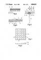
- FIG. 1is a plan view of the upper surface of the first layer of the carrier
- FIG. 2is the pattern of the intermediate layer
- FIG. 3is the pattern of holes in the lower layer
- FIG. 4is a cross-section through a pin array along line X--X of FIG. 1;
- FIG. 5is the detailed cross-section of the two principal layers of the carrier.
- FIG. 6is a detailed cross-section of the pin-head structure
- FIG. 7is a plan view of the grid arrangement of side walls
- FIG. 8is a cross-section along the line Y--Y of FIG. 6.
- Each individual carrierwill have an upper layer 10, an intermediate layer 11 and a lower layer 12.
- On layer 10is a chip pad 1 surrounded by a series of pads 2 with metal surface connections tracks or paths 3 formed to a series of points in zones at which points are formed metallised holes 4 the upper entrances to which are shown in FIG. 1 and shown in cross-section in FIG. 5.
- Each of those holesis formed with plated-through metallisation 5 to connect the connection 3 (which can end in a pad at the point in the zone) to a pad 6 in the intermediate layer 11. From each of fthese pads there extends a metal connector 7 inwardly or outwardly of the line of holes to a further pad 8.
- the lower layer 12consists of a pattern of openings 9 each of these openings has a plated-through metallisation 20 to provide a metallic contact around the periphery of the opening and connect pad 8 on the intermediate layer with a lower pad 21.
- each opening 9there is mounted head 22 of a pin 13 contact being provided between the head of the pin and the metallisation 20 in the opening 9.
- the top of the pinmay rest against the pad 8 in the upper layer.
- the upper surfaceis surrounded by a wall 14 on which may be placed a lid 15.
- the chip carriersare formed in series by initially forming by conventional printed circuit techniques the metallisation pattern of FIGS.
- the upper layera plastics material with copper on the upper side and as the lower a layer with copper on both sides.
- Pads, connectors and plated through metallisationare all formed by conventional techniques used in printed circuit board manufacture preferably from copper plating with gold or nickel-gold alloy.
- the pattern of the intermediate layer 11can be formed on the lower surface of the upper layer 10 by using a double sided copper printed circuit board material.
- the holes at 4can be drilled after the upper and lower layers are bonded together so then as to provide metallisation at least through the upper layer from pad at area 4 to lower pad 8. As shown in FIG. 6 the head 22 of the pin 13 extends into the opening 9.
- the openings in layer 12can be metallised after or preferably before bonding of the layers together. Extension of the holes 4 through the entire array eases metallisation because of the narrow diameter of the holes 4. The diameter of the larger holes 9 provided for the pin heads allows easier access for metallisation. It will be noted that the holes 4 are inwards of the outer limits of the pin array locations and the connections 7 extend outwardly and inwardly from the initial holes 4 so permitting a complete range of pins across the entire undersurface of the carrier.
- a third matrix grid 14preferably formed of the same material as the other two layers is bonded to the upper surface the arms of the grid extending along the peripheries of the proposed chip carriers covering the holes 4.
- Pinscan be loaded into the pin holders having for example, holes on an 2.5 millimeter (0.1 inch) array grid and the heads 9 of the pins can be fused into position using standard solder reflow methods to form solderbond 23.
- the pinscan be mounted into the openings 9 by solder paste applied to the pads 8 by conventional techniques silk screening methods.
- the pinscan be added to the assembly after separation of the individual pin grid assemblies as hereinafter described.
- the assembly of a series of pin grid arraysis cut into individually arrays thus separating to form the individual chip carriers using a diamond saw along the centre lines of the arms 14.
- Individual integrated circuit chipscan be mounted in a cavity or depression formed by the arms 14 of the grid before or after formation of the individual arrays.
- the cavitycan be filled with a layer of coating material made of a plastics material which serves to enclose and protect the chip.
- a cover sheet 15preferably formed of the same material as the base 10 may be secured over the walls 14 to form a protective cover known as a lid for each of the chip carriers.
- a further layer of coating materialcould be applied instead of the lid said coating material being the same or different from the basic coating material to provide additional protection for the chip.
- the resulting assemblycan then be mounted into a printed circuit board by insertion of the pins of the assembly into respective holes on the circuit board.
- the chip carriercan be made of conventional printed circuit board material and a whole series of arrays can be formed simultaneously.
- the coordination of the different layers and interconnection of the different padsis much more simple than handling individual arrays since there is use of the sheet up to the point at which the individual chip carriers are separated.
- a sheet with a series of arraysis much easier to handle than individual chip carriers and can readily be processed by automatic assembly apparatus including the drilling of the various holes, assembly of the pins and assembly, if desired, of the individual integrated circuit chips into the individual arrays.
- manufacture of the different layersby conventional glass/epoxy printed circuit board material and printing techniques allows well tried and tested techniques to be used and greatly reduces the cost of the final item.
- the individual chips mounted in the central chip padscan be connected to the pads 2 for the surrounding connectors by conventional techniques such as wire bonding, the chips or dies being bonded to the base by means of an epoxy adhesive compatible with the material of the base.
- the number and disposition of the pads and underlying pin arrayscan be determined in advance so as to correspond to the desired pin array for the corresponding circuit board.
Landscapes
- Physics & Mathematics (AREA)
- Condensed Matter Physics & Semiconductors (AREA)
- General Physics & Mathematics (AREA)
- Engineering & Computer Science (AREA)
- Computer Hardware Design (AREA)
- Microelectronics & Electronic Packaging (AREA)
- Power Engineering (AREA)
- Lead Frames For Integrated Circuits (AREA)
Abstract
Description
Claims (1)
Applications Claiming Priority (2)
| Application Number | Priority Date | Filing Date | Title |
|---|---|---|---|
| GB8721779AGB2209867B (en) | 1987-09-16 | 1987-09-16 | Method of forming an integrated circuit chip carrier |
| GB8721779 | 1987-09-16 |
Publications (1)
| Publication Number | Publication Date |
|---|---|
| US4866841Atrue US4866841A (en) | 1989-09-19 |
Family
ID=10623876
Family Applications (1)
| Application Number | Title | Priority Date | Filing Date |
|---|---|---|---|
| US07/244,959Expired - Fee RelatedUS4866841A (en) | 1987-09-16 | 1988-09-15 | Integrated circuit chip carrier |
Country Status (2)
| Country | Link |
|---|---|
| US (1) | US4866841A (en) |
| GB (1) | GB2209867B (en) |
Cited By (14)
| Publication number | Priority date | Publication date | Assignee | Title |
|---|---|---|---|---|
| US5379191A (en)* | 1991-02-26 | 1995-01-03 | Microelectronics And Computer Technology Corporation | Compact adapter package providing peripheral to area translation for an integrated circuit chip |
| US5485039A (en)* | 1991-12-27 | 1996-01-16 | Hitachi, Ltd. | Semiconductor substrate having wiring conductors at a first main surface electrically connected to plural pins at a second main surface |
| EP0692823A1 (en)* | 1994-07-11 | 1996-01-17 | Sun Microsystems, Inc. | Ball grid array package for an integated circuit |
| US5621190A (en)* | 1993-12-24 | 1997-04-15 | Ngk Spark Plug Co., Ltd. | Ceramic package main body |
| US5679977A (en)* | 1990-09-24 | 1997-10-21 | Tessera, Inc. | Semiconductor chip assemblies, methods of making same and components for same |
| US5682061A (en)* | 1990-09-24 | 1997-10-28 | Tessera, Inc. | Component for connecting a semiconductor chip to a substrate |
| US5861663A (en)* | 1994-12-27 | 1999-01-19 | International Business Machines Corporation | Column grid array or ball grid array pad on via |
| US6115914A (en)* | 1996-03-18 | 2000-09-12 | Maxtor Corporation | Method for attaching a substrate to an in-line electrical connector |
| US6133627A (en)* | 1990-09-24 | 2000-10-17 | Tessera, Inc. | Semiconductor chip package with center contacts |
| US20020053452A1 (en)* | 1996-09-04 | 2002-05-09 | Quan Son Ky | Semiconductor package and method therefor |
| US20040129452A1 (en)* | 1994-12-05 | 2004-07-08 | Owens Norman Lee | Multi-strand substrate for ball-grid array assemblies and method |
| US7098078B2 (en) | 1990-09-24 | 2006-08-29 | Tessera, Inc. | Microelectronic component and assembly having leads with offset portions |
| US20080101045A1 (en)* | 2006-10-30 | 2008-05-01 | Samsung Electro-Mechanics Co., Ltd. | Circuit board and manufacturing method thereof |
| US20110067899A1 (en)* | 2009-09-22 | 2011-03-24 | Samsung Electro-Mechanics Co., Ltd. | Lead pin for package substrate |
Families Citing this family (2)
| Publication number | Priority date | Publication date | Assignee | Title |
|---|---|---|---|---|
| US4887148A (en)* | 1988-07-15 | 1989-12-12 | Advanced Micro Devices, Inc. | Pin grid array package structure |
| DE3923533A1 (en)* | 1989-07-15 | 1991-01-24 | Diehl Gmbh & Co | ARRANGEMENT OF AN INTEGRATED CIRCUIT ON A CIRCUIT BOARD |
Citations (6)
| Publication number | Priority date | Publication date | Assignee | Title |
|---|---|---|---|---|
| US4393581A (en)* | 1980-01-22 | 1983-07-19 | Amp Incorporated | Method of forming leads on a lead frame |
| US4461529A (en)* | 1982-06-16 | 1984-07-24 | W. L. Gore & Associates, Inc. | Strain relief boot |
| US4513355A (en)* | 1983-06-15 | 1985-04-23 | Motorola, Inc. | Metallization and bonding means and method for VLSI packages |
| US4618739A (en)* | 1985-05-20 | 1986-10-21 | General Electric Company | Plastic chip carrier package |
| US4677526A (en)* | 1984-03-01 | 1987-06-30 | Augat Inc. | Plastic pin grid array chip carrier |
| US4823234A (en)* | 1985-08-16 | 1989-04-18 | Dai-Ichi Seiko Co., Ltd. | Semiconductor device and its manufacture |
Family Cites Families (9)
| Publication number | Priority date | Publication date | Assignee | Title |
|---|---|---|---|---|
| JPS5128829B1 (en)* | 1968-10-21 | 1976-08-21 | ||
| US4074342A (en)* | 1974-12-20 | 1978-02-14 | International Business Machines Corporation | Electrical package for lsi devices and assembly process therefor |
| US4221047A (en)* | 1979-03-23 | 1980-09-09 | International Business Machines Corporation | Multilayered glass-ceramic substrate for mounting of semiconductor device |
| US4322778A (en)* | 1980-01-25 | 1982-03-30 | International Business Machines Corp. | High performance semiconductor package assembly |
| US4338621A (en)* | 1980-02-04 | 1982-07-06 | Burroughs Corporation | Hermetic integrated circuit package for high density high power applications |
| US4302625A (en)* | 1980-06-30 | 1981-11-24 | International Business Machines Corp. | Multi-layer ceramic substrate |
| JPS5816552A (en)* | 1981-07-22 | 1983-01-31 | Fujitsu Ltd | Package for semiconductor devices |
| US4446477A (en)* | 1981-08-21 | 1984-05-01 | Sperry Corporation | Multichip thin film module |
| JPS5987893A (en)* | 1982-11-12 | 1984-05-21 | 株式会社日立製作所 | A wiring board, its manufacturing method, and a semiconductor device using the same |
- 1987
- 1987-09-16GBGB8721779Apatent/GB2209867B/ennot_activeExpired - Lifetime
- 1988
- 1988-09-15USUS07/244,959patent/US4866841A/ennot_activeExpired - Fee Related
Patent Citations (6)
| Publication number | Priority date | Publication date | Assignee | Title |
|---|---|---|---|---|
| US4393581A (en)* | 1980-01-22 | 1983-07-19 | Amp Incorporated | Method of forming leads on a lead frame |
| US4461529A (en)* | 1982-06-16 | 1984-07-24 | W. L. Gore & Associates, Inc. | Strain relief boot |
| US4513355A (en)* | 1983-06-15 | 1985-04-23 | Motorola, Inc. | Metallization and bonding means and method for VLSI packages |
| US4677526A (en)* | 1984-03-01 | 1987-06-30 | Augat Inc. | Plastic pin grid array chip carrier |
| US4618739A (en)* | 1985-05-20 | 1986-10-21 | General Electric Company | Plastic chip carrier package |
| US4823234A (en)* | 1985-08-16 | 1989-04-18 | Dai-Ichi Seiko Co., Ltd. | Semiconductor device and its manufacture |
Cited By (36)
| Publication number | Priority date | Publication date | Assignee | Title |
|---|---|---|---|---|
| US7098078B2 (en) | 1990-09-24 | 2006-08-29 | Tessera, Inc. | Microelectronic component and assembly having leads with offset portions |
| US5848467A (en)* | 1990-09-24 | 1998-12-15 | Tessera, Inc. | Methods of making semiconductor chip assemblies |
| US7291910B2 (en) | 1990-09-24 | 2007-11-06 | Tessera, Inc. | Semiconductor chip assemblies, methods of making same and components for same |
| US7271481B2 (en) | 1990-09-24 | 2007-09-18 | Tessera, Inc. | Microelectronic component and assembly having leads with offset portions |
| US7198969B1 (en) | 1990-09-24 | 2007-04-03 | Tessera, Inc. | Semiconductor chip assemblies, methods of making same and components for same |
| US5679977A (en)* | 1990-09-24 | 1997-10-21 | Tessera, Inc. | Semiconductor chip assemblies, methods of making same and components for same |
| US6372527B1 (en) | 1990-09-24 | 2002-04-16 | Tessera, Inc. | Methods of making semiconductor chip assemblies |
| US6392306B1 (en) | 1990-09-24 | 2002-05-21 | Tessera, Inc. | Semiconductor chip assembly with anisotropic conductive adhesive connections |
| US6133627A (en)* | 1990-09-24 | 2000-10-17 | Tessera, Inc. | Semiconductor chip package with center contacts |
| US5685885A (en)* | 1990-09-24 | 1997-11-11 | Tessera, Inc. | Wafer-scale techniques for fabrication of semiconductor chip assemblies |
| US5682061A (en)* | 1990-09-24 | 1997-10-28 | Tessera, Inc. | Component for connecting a semiconductor chip to a substrate |
| US6465893B1 (en) | 1990-09-24 | 2002-10-15 | Tessera, Inc. | Stacked chip assembly |
| US5950304A (en)* | 1990-09-24 | 1999-09-14 | Tessera, Inc. | Methods of making semiconductor chip assemblies |
| US6433419B2 (en) | 1990-09-24 | 2002-08-13 | Tessera, Inc. | Face-up semiconductor chip assemblies |
| US5379191A (en)* | 1991-02-26 | 1995-01-03 | Microelectronics And Computer Technology Corporation | Compact adapter package providing peripheral to area translation for an integrated circuit chip |
| US5485039A (en)* | 1991-12-27 | 1996-01-16 | Hitachi, Ltd. | Semiconductor substrate having wiring conductors at a first main surface electrically connected to plural pins at a second main surface |
| US5822851A (en)* | 1993-12-24 | 1998-10-20 | Ngk Spark Plug Co., Ltd. | Method of producing a ceramic package main body |
| US5621190A (en)* | 1993-12-24 | 1997-04-15 | Ngk Spark Plug Co., Ltd. | Ceramic package main body |
| US6077728A (en)* | 1993-12-24 | 2000-06-20 | Ngk Spark Plug Co., Ltd. | Method of producing a ceramic package main body |
| EP0692823A1 (en)* | 1994-07-11 | 1996-01-17 | Sun Microsystems, Inc. | Ball grid array package for an integated circuit |
| US5741729A (en)* | 1994-07-11 | 1998-04-21 | Sun Microsystems, Inc. | Ball grid array package for an integrated circuit |
| US5640048A (en)* | 1994-07-11 | 1997-06-17 | Sun Microsystems, Inc. | Ball grid array package for a integrated circuit |
| US20080289867A1 (en)* | 1994-12-05 | 2008-11-27 | Freescale Semiconductor, Inc. | Multi-strand substrate for ball-grid array assemblies and method |
| US7397001B2 (en) | 1994-12-05 | 2008-07-08 | Freescale Semiconductor, Inc. | Multi-strand substrate for ball-grid array assemblies and method |
| US20040129452A1 (en)* | 1994-12-05 | 2004-07-08 | Owens Norman Lee | Multi-strand substrate for ball-grid array assemblies and method |
| US7199306B2 (en) | 1994-12-05 | 2007-04-03 | Freescale Semiconductor, Inc. | Multi-strand substrate for ball-grid array assemblies and method |
| US20070137889A1 (en)* | 1994-12-05 | 2007-06-21 | Owens Norman L | Multi-strand substrate for ball-grid array assemblies and method |
| US5861663A (en)* | 1994-12-27 | 1999-01-19 | International Business Machines Corporation | Column grid array or ball grid array pad on via |
| US6127204A (en)* | 1994-12-27 | 2000-10-03 | International Business Machines Corporation | Column grid array or ball grid array pad on via |
| US6115914A (en)* | 1996-03-18 | 2000-09-12 | Maxtor Corporation | Method for attaching a substrate to an in-line electrical connector |
| US20020053452A1 (en)* | 1996-09-04 | 2002-05-09 | Quan Son Ky | Semiconductor package and method therefor |
| US7927927B2 (en) | 1996-09-04 | 2011-04-19 | Freescale Semiconductor, Inc. | Semiconductor package and method therefor |
| US20080101045A1 (en)* | 2006-10-30 | 2008-05-01 | Samsung Electro-Mechanics Co., Ltd. | Circuit board and manufacturing method thereof |
| US7992291B2 (en)* | 2006-10-30 | 2011-08-09 | Samsung Electro-Mechanics Co., Ltd. | Method of manufacturing a circuit board |
| US20110067899A1 (en)* | 2009-09-22 | 2011-03-24 | Samsung Electro-Mechanics Co., Ltd. | Lead pin for package substrate |
| US8420955B2 (en)* | 2009-09-22 | 2013-04-16 | Samsung Electro-Mechanics Co., Ltd. | Lead pin for package substrate |
Also Published As
| Publication number | Publication date |
|---|---|
| GB2209867B (en) | 1990-12-19 |
| GB2209867A (en) | 1989-05-24 |
| GB8721779D0 (en) | 1987-10-21 |
Similar Documents
| Publication | Publication Date | Title |
|---|---|---|
| US4866841A (en) | Integrated circuit chip carrier | |
| US4448306A (en) | Integrated circuit chip carrier | |
| US5172303A (en) | Electronic component assembly | |
| US5677515A (en) | Shielded multilayer printed wiring board, high frequency, high isolation | |
| US5886876A (en) | Surface-mounted semiconductor package and its manufacturing method | |
| US4700276A (en) | Ultra high density pad array chip carrier | |
| CA1214537A (en) | Integrated circuit module and method of making same | |
| US5006673A (en) | Fabrication of pad array carriers from a universal interconnect structure | |
| US5264729A (en) | Semiconductor package having programmable interconnect | |
| US20020125042A1 (en) | Method for transforming a substrate with edge contacts into a ball grid array, ball grid array manufactured according to this method, and flexible wiring for the transformation of a substrate with edge contacts into a ball grid array | |
| EP0524761A1 (en) | Plastic pin grid array package | |
| EP1168447A2 (en) | Multi-layered semiconductor device and method | |
| WO1987004316A1 (en) | Ultra high density pad array chip carrier | |
| US7399661B2 (en) | Method for making an integrated circuit substrate having embedded back-side access conductors and vias | |
| JP2002524857A (en) | Via plug adapter | |
| US5124783A (en) | Semiconductor device having insulating substrate adhered to conductive substrate | |
| US5245135A (en) | Stackable high density interconnection mechanism (SHIM) | |
| EP0139431B1 (en) | Method of mounting a carrier for a microelectronic silicon chip | |
| US4933810A (en) | Integrated circuit interconnector | |
| US6784376B1 (en) | Solderable injection-molded integrated circuit substrate and method therefor | |
| US6609915B2 (en) | Interconnect for electrically connecting a multichip module to a circuit substrate and processes for making and using same | |
| WO2003005782A2 (en) | Stackable microcircuit and method of making the same | |
| AU611127B2 (en) | Method for connecting leadless chip packages and articles | |
| US4829405A (en) | Tape automated bonding package | |
| US4860443A (en) | Method for connecting leadless chip package |
Legal Events
| Date | Code | Title | Description |
|---|---|---|---|
| AS | Assignment | Owner name:TECTONIC PRODUCTS LIMITED, OXFORD ROAD, WOKINGHAM, Free format text:ASSIGNMENT OF ASSIGNORS INTEREST.;ASSIGNOR:HUBBARD, JOHN B.;REEL/FRAME:004987/0537 Effective date:19880930 Owner name:ADVANCED SEMICONDUCTOR PACKAGES LTD, C/O HYCOMP LT Free format text:ASSIGNMENT OF ASSIGNORS INTEREST.;ASSIGNOR:TECTONIC PRODUCTS LIMITED;REEL/FRAME:004987/0539 Effective date:19880930 Owner name:TECTONIC PRODUCTS LIMITED, ENGLAND Free format text:ASSIGNMENT OF ASSIGNORS INTEREST;ASSIGNOR:HUBBARD, JOHN B.;REEL/FRAME:004987/0537 Effective date:19880930 Owner name:ADVANCED SEMICONDUCTOR PACKAGES LTD, C/O HYCOMP LT Free format text:ASSIGNMENT OF ASSIGNORS INTEREST;ASSIGNOR:TECTONIC PRODUCTS LIMITED;REEL/FRAME:004987/0539 Effective date:19880930 | |
| REMI | Maintenance fee reminder mailed | ||
| LAPS | Lapse for failure to pay maintenance fees | ||
| FP | Lapsed due to failure to pay maintenance fee | Effective date:19930919 | |
| STCH | Information on status: patent discontinuation | Free format text:PATENT EXPIRED DUE TO NONPAYMENT OF MAINTENANCE FEES UNDER 37 CFR 1.362 |