US4864126A - Solid state relay with optically controlled shunt and series enhancement circuit - Google Patents
Solid state relay with optically controlled shunt and series enhancement circuitDownload PDFInfo
- Publication number
- US4864126A US4864126AUS07/207,809US20780988AUS4864126AUS 4864126 AUS4864126 AUS 4864126AUS 20780988 AUS20780988 AUS 20780988AUS 4864126 AUS4864126 AUS 4864126A
- Authority
- US
- United States
- Prior art keywords
- solid state
- switch means
- output device
- state relay
- emitting diode
- Prior art date
- Legal status (The legal status is an assumption and is not a legal conclusion. Google has not performed a legal analysis and makes no representation as to the accuracy of the status listed.)
- Expired - Lifetime
Links
Images


Classifications
- H—ELECTRICITY
- H01—ELECTRIC ELEMENTS
- H01H—ELECTRIC SWITCHES; RELAYS; SELECTORS; EMERGENCY PROTECTIVE DEVICES
- H01H51/00—Electromagnetic relays
- H—ELECTRICITY
- H03—ELECTRONIC CIRCUITRY
- H03K—PULSE TECHNIQUE
- H03K17/00—Electronic switching or gating, i.e. not by contact-making and –breaking
- H03K17/51—Electronic switching or gating, i.e. not by contact-making and –breaking characterised by the components used
- H03K17/56—Electronic switching or gating, i.e. not by contact-making and –breaking characterised by the components used by the use, as active elements, of semiconductor devices
- H03K17/687—Electronic switching or gating, i.e. not by contact-making and –breaking characterised by the components used by the use, as active elements, of semiconductor devices the devices being field-effect transistors
- H03K17/6871—Electronic switching or gating, i.e. not by contact-making and –breaking characterised by the components used by the use, as active elements, of semiconductor devices the devices being field-effect transistors the output circuit comprising more than one controlled field-effect transistor
- H03K17/6874—Electronic switching or gating, i.e. not by contact-making and –breaking characterised by the components used by the use, as active elements, of semiconductor devices the devices being field-effect transistors the output circuit comprising more than one controlled field-effect transistor in a symmetrical configuration
- H—ELECTRICITY
- H03—ELECTRONIC CIRCUITRY
- H03K—PULSE TECHNIQUE
- H03K17/00—Electronic switching or gating, i.e. not by contact-making and –breaking
- H03K17/04—Modifications for accelerating switching
- H03K17/042—Modifications for accelerating switching by feedback from the output circuit to the control circuit
- H03K17/04206—Modifications for accelerating switching by feedback from the output circuit to the control circuit in field-effect transistor switches
- H—ELECTRICITY
- H03—ELECTRONIC CIRCUITRY
- H03K—PULSE TECHNIQUE
- H03K17/00—Electronic switching or gating, i.e. not by contact-making and –breaking
- H03K17/16—Modifications for eliminating interference voltages or currents
- H03K17/161—Modifications for eliminating interference voltages or currents in field-effect transistor switches
- H03K17/162—Modifications for eliminating interference voltages or currents in field-effect transistor switches without feedback from the output circuit to the control circuit
- H—ELECTRICITY
- H03—ELECTRONIC CIRCUITRY
- H03K—PULSE TECHNIQUE
- H03K17/00—Electronic switching or gating, i.e. not by contact-making and –breaking
- H03K17/16—Modifications for eliminating interference voltages or currents
- H03K17/161—Modifications for eliminating interference voltages or currents in field-effect transistor switches
- H03K17/165—Modifications for eliminating interference voltages or currents in field-effect transistor switches by feedback from the output circuit to the control circuit
- H—ELECTRICITY
- H03—ELECTRONIC CIRCUITRY
- H03K—PULSE TECHNIQUE
- H03K17/00—Electronic switching or gating, i.e. not by contact-making and –breaking
- H03K17/51—Electronic switching or gating, i.e. not by contact-making and –breaking characterised by the components used
- H03K17/78—Electronic switching or gating, i.e. not by contact-making and –breaking characterised by the components used using opto-electronic devices, i.e. light-emitting and photoelectric devices electrically- or optically-coupled
- H03K17/785—Electronic switching or gating, i.e. not by contact-making and –breaking characterised by the components used using opto-electronic devices, i.e. light-emitting and photoelectric devices electrically- or optically-coupled controlling field-effect transistor switches
Definitions
- a solid state relayprovides isolation between a control circuit and a switched circuit and may replace an electromechanical device such as a reed relay.
- a typical solid state relayconsists of a light emitting diode (LED) optically coupled across an electrically isolating gap to a photodiode array.
- the photodiode arrayis electrically connected to a output device such as a field effect transistor (FET).
- FETfield effect transistor
- the relay disclosed in U.S. Pat. No. 4,390,790 to Rodriguezincludes a photodiode array directly connected to an output FET.
- Rodriguez's use of a turnoff transistor to discharge the output FET gate to source capacitanceprovides some improvement in turn-off speed but provides no transient protection to the relay.
- Relays such as thisare vulnerable not only to transient propagation between the control and switched circuits but also to transient induced false turn-on and turn-off.
- a solid state relayhas improved turn-off characteristics and a high degree of transient immunity.
- the relayincludes an optically controlled active series and shunt enhancement circuit located between the photodiode array and a pair of output FETs.
- Series phototransistors in the enhancement circuitactively couple and decouple the array from the output FETs at turn-on and turn-off.
- a shunt FET and a shunt silicon controlled rectifier (SCR)create rapid discharge paths for the output FET gate to source capacitances at turn-off.
- a shunt transistoris capacitively coupled to the relay output to protect against transient induced false turn-ons.
- the solid state relayincludes a shield over the photodiode array.
- Use of the shieldallows direct and close optical coupling between the LED and the photodiode array so that high speed can be achieved at low required LED currents.
- the shieldis both optically transmissive and electrically conductive and is connected to ground or to another neutral part of the relay circuit. The shield is positioned to intercept control circuit transients so that false turn-on caused by electrical activation of the photodiode array or other components can be avoided.
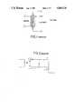
- FIG. 1shows a prior art mechanical relay.
- FIGS. 2 and 3show prior art solid state relays.
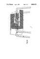
- FIG. 4is a cut away view of the package of a solid state relay constructed in accordance with the preferred embodiment of the present invention.
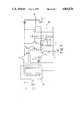
- FIG. 5is a schematic diagram of the solid state relay shown in FIG. 4.
- FIG. 6shows a block diagram representation of the enhancement circuit shown in FIG. 5.
- FIG. 7is a schematic diagram of an alternate preferred embodiment of the present invention in which a shield is used.
- FIG. 8is a cut away view of a portion of the physical circuit depicted in FIG. 7.
- FIG. 1shows a well known reed relay that may be used to provide isolation between a control circuit and a switched circuit.
- Electromechanical devicessuch as reed relays have inherent disadvantages due to the use of mechanical moving parts.
- FIG. 2is a schematic diagram of a prior art solid state relay disclosed by Rodriguez in U.S. Pat. No. 4,390,790. Activation of the LED by the control circuit creates a voltage across the photodiode array which turns on the output FETs. The shunt resistor accelerates the discharge of the FET capacitances at turn-off but slows turn-on of the relay.
- FIG. 3is a schematic diagram of another prior art solid state relay disclosed by the Rodriguez patent. The shunt resistor is replaced by a shunt FET which is activated by a second photodiode array.
- FIG. 4is a cut-away view of a packaged solid state relay 1 constructed in accordance with a preferred embodiment of the present invention.
- the relay 1may be constructed using known lead frame technology of the type disclosed in U.S. Pat. No. 4,694,183 issued on Sept. 15, 1987 to Merrick, et. al.
- An LED 3is separated from an integrated circuit (IC) 5 containing the remainder of the relay circuitry by a gap 9 including an optically transmissive light guide 11 and an insulating film 7.
- Total relay 1 input to output resistanceis approximately 50 gigaohms.
- LED 3could be located in the same plane as IC 5 and gap 9 would then be a curved path rather than the straight path shown in FIG. 4 for face-to-face positioning.
- FIG. 5is a schematic diagram of the relay 1 shown in FIG. 4.
- the entire circuit, except for LED 3,is fabricated as one IC 5 on a single silicon chip.
- Known dielectric isolation techniquesdescribed in U.S. Pat. No. 4,390,790 are used to provide necessary electrical isolation between various components of the circuit.
- a photodiode array 13has ten individual photodiodes and generates an on-voltage of approximately 5 volts in response to a 5 mA current through LED 3. This on-voltage is coupled, through phototransistors 33 and 35, across the gates-to-sources of output FETs 15 and 17.
- These output FETs 15, 17are vertical double diffused MOS (DMOS) devices constructed in dielectric isolation tubs.
- DMOSvertical double diffused MOS
- the sources of the two FETs 13, 15are connected together to achieve the desired high, 230 volt, bilateral breakdown voltage despite the existence of parasitic diodes between the sources and drains.
- Output on-resistanceis approximately 200 ohms.
- Output terminals 19, 21provide a low impedance path when the relay 1 is on and allow connection to the circuit to be switched.
- Source terminal 23may be a ground or neutral connection of the switched circuit. The voltage at terminal 23 will remain one diode drop voltage (about 0.7 volts) above the lower of the voltages at terminal 19 or 21. Alternatively, in D.C. switching (between terminal 23 and either of terminals 19 or 21) terminal 23 will remain at the most negative voltage of any of the three terminals.
- FIG. 6is a block diagram representation of an enhancement circuit 31 located between the array 13 and the output FETs 15, 17 shown in FIG. 5.
- the enhancement circuit 31provides enhanced turn-on less (less than 250 microseconds), turn-off (less than 100 microseconds) and transient immunity characteristics to the relay 1.
- circuit 31may be. modelled as a series and shunt combination of optically controlled active switches including series switches 41, 43 and shunt switches 45, 47 and 49.
- Switches 41 and 43are two series phototransistors 33, 35 which couple and decouple the gates and sources of the output FETs 15, 17 from the photodiode array 13.
- Switch 45is a silicon controlled rectifier 51 made up of transistors 53, 55. SCR 51 is connected from gates to sources of the output FETs 15, 17 and is controlled by the phototransistors 33, 35 and a FET 61.
- the base-emitter junction of pnp transistor 57is connected across phototransistor 33 and the collector is connected to the gate of FET 61.
- Switch 47is a transistor 63 connected across the gate to source path of the output FETs 15, 17.
- the base of transistor 63is capacitively coupled through capacitors 65, 67 to the output terminals 19, 21, and is also connected to the drain of a FET 69.
- Photodiodes 71, 73are activated by light from LED 3 and are connected from the gate to the source of FET 69.
- Switch 49is a FET 75 shunting the gate to source of the output FETs 15, 17 and controlled by photodiodes 71, 73.
- a currentis passed through LED 3 causing it to emit light.
- This lightis coupled across gap 9 to array 13 which presents a nominal 5 volts at the input to enhancement circuit 31.
- the lightalso activates phototransistors 33, 35 which couple the array 13 voltage to output FETs 15, 17.
- This voltagesignificantly exceeds the 1.1 volt threshhold of the FETs 15, 17 and ensures turn-on.
- the light from LED 3illuminates photodiodes 71, 73 and causes them to generate a voltage of approximately 1 volt.
- This voltageturns off FET 75 (shunt switch 49) and FET 61 and turns on FET 69 which shunts the base-emitter junction of transistor 63 (switch 47) and turns it off.
- transistor 63When this occurs, the drain of one of the output FETs begins to move towards a positive voltage and this voltage change, through capacitor 65 or 67, causes transistor 63 to turn on. Conduction of transistor 63 further shunts the gates to sources of output FETs 15, 17. Current stops flowing in transistor 63 when the voltage change at terminals 19, 21 ceases.
- Enhancement circuit 31also provides significant transient protection to relay 1. In the off-state, a transient at either output terminal 19, 21 is capacitively coupled to the base of transistor 63 (shunt switch 49). This ensures that transistor 63 is turned on and precludes unintentional turn-on of either output FET 15, 17.
- Phototransistors 33, 35provide on-state protection against unintentional turn-off due to a transient in the control circuit. The pnp phototransistors 33, 35 are symmetric and conduct equally well in the forward and reverse modes so that they continue to hold the SCR 51 off even in the presence of input transients.
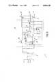
- FIG. 7shows an alternate preferred embodiment of the present invention in which shields 91, 93 provide additional transient protection for relay 1.
- Shield 91overlays photodiode array 13 and lies between array 13 and LED 3.
- Shield 93overlays photodiodes 71, 73 and lies between photodiodes 71, 73 and LED 3.
- Both shields 91, 93are physically connected to source terminal 21 or may be connected to a ground or neutral terminal of the circuit.
- Shields 91, .93are most advantageous if LED 3 and array 13 are positioned across a gap 9 instead of being coplanar. This face-to-face alignment allows maximum optical coupling and minimum required LED 3 drive current. It also increases undesired LED 3 to IC 5 capacitive coupling which increases transient susceptibility.
- Shields 91 and 93are optically transmissive and electrically conductive and may be viewed as Faraday shields in that they are conductive plates or ground planes that act to terminate electrical field lines emanating from the control circuit. Without shields 91, 93 an electrical transient entering relay 1 from the control circuit through the LED 3 connections could be capacitively coupled into the circuitry of relay 1 beyond array 11. The transient, positive or negative, could cause an unwanted false turn-on or turn-off of relay 1. With shields 91, 93 in place a positive or negative input transient is terminated on shield 91 or 93 and is shunted away from enhancement circuit 31 and the output FETs 15, 17.
- FIG. 7also shows a shadow mask 95 which overlays all of the active elements in IC 5 except for the areas covered by shields 91, 93 and phototransistors 33, 35.
- Shadow mask 95is an optically absorbing layer that protects optically sensitive components such as SCR 51 from inadvertent turn on due to illumination by LED 3.
- Shadow mask 95may be fabricated in accordance with the techniques disclosed in copending U.S. patent application Ser. No. 149,766 filed on Jan. 29, 1988.
- FIG. 8is a cut-away view of IC 5 showing three of the photodiodes of array 13 in cross section.
- the individual photodiodes of array 13are fabricated in a 500 micron thick polysilicon substrate 101 using dielectric isolation techniques similar to those used in fabrication of the Dionics Corporation model DIG-12-08-010 MOSFET Driver.
- Oxide liners 103provide 25 micron deep tubs that allow dielectric isolation between each of the individual photodiodes.
- Overlaying the entire IC 5are conventional passivation layers, which are optically transmissive, used in integrated circuit processing.
- An initial oxide layer 105is followed by a nitride layer 111.
- a polysilicon layer 107overlays the oxide layer 105 over the array 13 and the photodiodes 71, 73 to form shields 91, 93.
- a second oxide layer 109is used in these areas to separate the polysilicon layer 107 from the nitride layer 111
- the polysilicon layer 107is approximately one-half micron thick. A thinner layer might have conformance difficulties over surface irregularities and would have increased electrical resistance. A thicker layer would cause increased optical attenuation. The half micron thickness provides a good operational compromise between the electrical and optical conditions.
- the polysilicon layer 107transmits light best at wavelengths above 750 nanometers and has low optical attenuation at the 880 nanometer emission wavelength of LED 3. For lower emission wavelengths, other optically and electrically conductive materials such as indium tin oxide might be possible.
- the polysilicon layer 107may be deposited to form shields 91, 93 during the same processing step as the formation of the polysilicon gate regions of output FETs 15, 17 which may be similar to the IR Corporation IRF610 n-channel FET. If desired, the processing steps could be modified to allow deposition of another polysilicon shield layer over other optically active components such as phototransistors 33, 35. Contacts may be etched into shields 91, 93 to allow deposition of metal traces to connect shields 91, 93 to source terminal 23 as shown in FIG. 7. Metal conductors 113, 115 through layers 105-111 allow electrical connection to the individual photodiodes of array 13.
Landscapes
- Physics & Mathematics (AREA)
- Electromagnetism (AREA)
- Electronic Switches (AREA)
- Optical Modulation, Optical Deflection, Nonlinear Optics, Optical Demodulation, Optical Logic Elements (AREA)
Abstract
Description
Claims (16)
Priority Applications (6)
| Application Number | Priority Date | Filing Date | Title |
|---|---|---|---|
| US07/207,809US4864126A (en) | 1988-06-17 | 1988-06-17 | Solid state relay with optically controlled shunt and series enhancement circuit |
| EP19890104238EP0346571A3 (en) | 1988-06-17 | 1989-03-10 | Solid state relay |
| CA000593627ACA1298358C (en) | 1988-06-17 | 1989-03-14 | Solid state relay |
| US07/366,090US4939375A (en) | 1988-06-17 | 1989-06-13 | Solid state relay with shield means |
| JP1154407AJPH0239723A (en) | 1988-06-17 | 1989-06-16 | Solid relay |
| KR1019890008316AKR900000945A (en) | 1988-06-17 | 1989-06-16 | Solid state relay |
Applications Claiming Priority (1)
| Application Number | Priority Date | Filing Date | Title |
|---|---|---|---|
| US07/207,809US4864126A (en) | 1988-06-17 | 1988-06-17 | Solid state relay with optically controlled shunt and series enhancement circuit |
Related Child Applications (1)
| Application Number | Title | Priority Date | Filing Date |
|---|---|---|---|
| US07/366,090DivisionUS4939375A (en) | 1988-06-17 | 1989-06-13 | Solid state relay with shield means |
Publications (1)
| Publication Number | Publication Date |
|---|---|
| US4864126Atrue US4864126A (en) | 1989-09-05 |
Family
ID=22772084
Family Applications (1)
| Application Number | Title | Priority Date | Filing Date |
|---|---|---|---|
| US07/207,809Expired - LifetimeUS4864126A (en) | 1988-06-17 | 1988-06-17 | Solid state relay with optically controlled shunt and series enhancement circuit |
Country Status (5)
| Country | Link |
|---|---|
| US (1) | US4864126A (en) |
| EP (1) | EP0346571A3 (en) |
| JP (1) | JPH0239723A (en) |
| KR (1) | KR900000945A (en) |
| CA (1) | CA1298358C (en) |
Cited By (18)
| Publication number | Priority date | Publication date | Assignee | Title |
|---|---|---|---|---|
| US5061859A (en)* | 1989-09-13 | 1991-10-29 | Hewlett-Packard Company | Circuits for realizing an optical isolator |
| US5146100A (en)* | 1991-05-21 | 1992-09-08 | Keithley Instruments, Inc. | High voltage solid-state switch with current limit |
| US5278422A (en)* | 1991-09-02 | 1994-01-11 | Matsushita Electric Works, Ltd. | Normally open solid state relay with minimized response time of relay action upon being turned off |
| US5298817A (en)* | 1993-02-09 | 1994-03-29 | At&T Bell Laboratories | High-frequency solid-state relay |
| FR2702608A1 (en)* | 1993-03-09 | 1994-09-16 | Motorola Semiconducteurs | Circuit layout with switching transistor |
| US5360979A (en)* | 1993-08-05 | 1994-11-01 | At&T Bell Laboratories | Fast turn-off circuit for solid-state relays or the like |
| US5532498A (en)* | 1994-12-06 | 1996-07-02 | At&T Corp. | High sensitivity control circuit for optical solid-state relays |
| US5549762A (en)* | 1995-01-13 | 1996-08-27 | International Rectifier Corporation | Photovoltaic generator with dielectric isolation and bonded, insulated wafer layers |
| US5559466A (en)* | 1993-07-29 | 1996-09-24 | Kabushiki Kaisha Toshiba | Semiconductor relay for transmitting high frequency signals |
| US5592033A (en)* | 1993-12-16 | 1997-01-07 | Cooper Industries, Inc. | Photocell switching circuit |
| US5693952A (en)* | 1995-12-18 | 1997-12-02 | Sulzer Intermedics Inc. | Optically controlled high-voltage switch for an implantable defibrillator |
| EP0892438A3 (en)* | 1997-06-30 | 2000-09-13 | Matsushita Electric Works, Ltd. | Solid-state relay |
| US6153980A (en)* | 1999-11-04 | 2000-11-28 | Philips Electronics North America Corporation | LED array having an active shunt arrangement |
| US6184521B1 (en) | 1998-01-06 | 2001-02-06 | Masimo Corporation | Photodiode detector with integrated noise shielding |
| US20050052806A1 (en)* | 2003-09-05 | 2005-03-10 | Biotronik Gmbh & Co. Kg | Voltage-resistant MOS switch |
| US20060158042A1 (en)* | 2004-12-13 | 2006-07-20 | Ghildyal Subodh K | Photo controller for switching a load in a hazardous environment |
| US20150236057A1 (en)* | 2014-02-17 | 2015-08-20 | Renesas Electronics Corporation | Semiconductor device |
| US9374076B2 (en) | 2012-03-06 | 2016-06-21 | Mcq Inc. | Solid state relay circuit |
Families Citing this family (3)
| Publication number | Priority date | Publication date | Assignee | Title |
|---|---|---|---|---|
| US5198656A (en)* | 1991-06-06 | 1993-03-30 | At&T Bell Laboratories | Dynamic optical logic using voltage pull up |
| DE10227310A1 (en)* | 2002-06-19 | 2004-01-15 | Siemens Ag | Semiconductor switching device |
| EP2165912B1 (en)* | 2008-09-19 | 2012-04-25 | Bombardier Transportation GmbH | Instability monitoring device and system, in particular for a rail vehicle |
Citations (8)
| Publication number | Priority date | Publication date | Assignee | Title |
|---|---|---|---|---|
| US4390790A (en)* | 1979-08-09 | 1983-06-28 | Theta-J Corporation | Solid state optically coupled electrical power switch |
| GB2154820A (en)* | 1984-01-23 | 1985-09-11 | Int Rectifier Corp | Photovoltaic relay |
| US4564770A (en)* | 1983-03-29 | 1986-01-14 | Rca Corporation | Solid state relay with fast turnoff |
| JPS6215924A (en)* | 1985-07-12 | 1987-01-24 | Matsushita Electric Works Ltd | Semiconductor relay circuit |
| JPS6225511A (en)* | 1985-07-25 | 1987-02-03 | Matsushita Electric Works Ltd | Semiconductor relay |
| US4754175A (en)* | 1985-12-04 | 1988-06-28 | Nec Corporation | Solid state relay having a thyristor discharge circuit |
| US4777387A (en)* | 1984-02-21 | 1988-10-11 | International Rectifier Corporation | Fast turn-off circuit for photovoltaic driven MOSFET |
| US4804866A (en)* | 1986-03-24 | 1989-02-14 | Matsushita Electric Works, Ltd. | Solid state relay |
Family Cites Families (3)
| Publication number | Priority date | Publication date | Assignee | Title |
|---|---|---|---|---|
| FR2463543A1 (en)* | 1979-05-25 | 1981-02-20 | Dassault Electronique | MOSFET relay for telephone line switching - uses integrated capacitor and alternately illuminated photodiodes for gate control |
| US4665316A (en)* | 1984-11-21 | 1987-05-12 | Telmos Incorporated | Photovoltaic relay switch |
| US4746813A (en)* | 1987-06-04 | 1988-05-24 | General Motors Corporation | Switching circuit for inductive load with RFI suppression |
- 1988
- 1988-06-17USUS07/207,809patent/US4864126A/ennot_activeExpired - Lifetime
- 1989
- 1989-03-10EPEP19890104238patent/EP0346571A3/ennot_activeWithdrawn
- 1989-03-14CACA000593627Apatent/CA1298358C/ennot_activeExpired - Lifetime
- 1989-06-16JPJP1154407Apatent/JPH0239723A/enactivePending
- 1989-06-16KRKR1019890008316Apatent/KR900000945A/ennot_activeCeased
Patent Citations (8)
| Publication number | Priority date | Publication date | Assignee | Title |
|---|---|---|---|---|
| US4390790A (en)* | 1979-08-09 | 1983-06-28 | Theta-J Corporation | Solid state optically coupled electrical power switch |
| US4564770A (en)* | 1983-03-29 | 1986-01-14 | Rca Corporation | Solid state relay with fast turnoff |
| GB2154820A (en)* | 1984-01-23 | 1985-09-11 | Int Rectifier Corp | Photovoltaic relay |
| US4777387A (en)* | 1984-02-21 | 1988-10-11 | International Rectifier Corporation | Fast turn-off circuit for photovoltaic driven MOSFET |
| JPS6215924A (en)* | 1985-07-12 | 1987-01-24 | Matsushita Electric Works Ltd | Semiconductor relay circuit |
| JPS6225511A (en)* | 1985-07-25 | 1987-02-03 | Matsushita Electric Works Ltd | Semiconductor relay |
| US4754175A (en)* | 1985-12-04 | 1988-06-28 | Nec Corporation | Solid state relay having a thyristor discharge circuit |
| US4804866A (en)* | 1986-03-24 | 1989-02-14 | Matsushita Electric Works, Ltd. | Solid state relay |
Non-Patent Citations (2)
| Title |
|---|
| HEWLETT PACKARD COMPANY, Optoelectronics/Fiber Optics Applications Manual, Second Ed., 1981, pp. 3.5 3.9.* |
| HEWLETT-PACKARD COMPANY, Optoelectronics/Fiber Optics Applications Manual, Second Ed., 1981, pp. 3.5-3.9. |
Cited By (26)
| Publication number | Priority date | Publication date | Assignee | Title |
|---|---|---|---|---|
| US5061859A (en)* | 1989-09-13 | 1991-10-29 | Hewlett-Packard Company | Circuits for realizing an optical isolator |
| US5146100A (en)* | 1991-05-21 | 1992-09-08 | Keithley Instruments, Inc. | High voltage solid-state switch with current limit |
| US5278422A (en)* | 1991-09-02 | 1994-01-11 | Matsushita Electric Works, Ltd. | Normally open solid state relay with minimized response time of relay action upon being turned off |
| US5298817A (en)* | 1993-02-09 | 1994-03-29 | At&T Bell Laboratories | High-frequency solid-state relay |
| FR2702608A1 (en)* | 1993-03-09 | 1994-09-16 | Motorola Semiconducteurs | Circuit layout with switching transistor |
| US5559466A (en)* | 1993-07-29 | 1996-09-24 | Kabushiki Kaisha Toshiba | Semiconductor relay for transmitting high frequency signals |
| US5360979A (en)* | 1993-08-05 | 1994-11-01 | At&T Bell Laboratories | Fast turn-off circuit for solid-state relays or the like |
| US5592033A (en)* | 1993-12-16 | 1997-01-07 | Cooper Industries, Inc. | Photocell switching circuit |
| US5532498A (en)* | 1994-12-06 | 1996-07-02 | At&T Corp. | High sensitivity control circuit for optical solid-state relays |
| US5549762A (en)* | 1995-01-13 | 1996-08-27 | International Rectifier Corporation | Photovoltaic generator with dielectric isolation and bonded, insulated wafer layers |
| US5693952A (en)* | 1995-12-18 | 1997-12-02 | Sulzer Intermedics Inc. | Optically controlled high-voltage switch for an implantable defibrillator |
| EP0892438A3 (en)* | 1997-06-30 | 2000-09-13 | Matsushita Electric Works, Ltd. | Solid-state relay |
| US6580126B1 (en) | 1997-06-30 | 2003-06-17 | Matsushita Electric Works, Ltd. | Solid-state relay |
| US6211551B1 (en) | 1997-06-30 | 2001-04-03 | Matsushita Electric Works, Ltd. | Solid-state relay |
| KR100310479B1 (en)* | 1997-06-30 | 2001-11-30 | 이마이 기요스케 | Solid-state relay |
| US6373101B1 (en) | 1997-06-30 | 2002-04-16 | Matsushita Electric Works | Solid-state relay |
| US6184521B1 (en) | 1998-01-06 | 2001-02-06 | Masimo Corporation | Photodiode detector with integrated noise shielding |
| US6153980A (en)* | 1999-11-04 | 2000-11-28 | Philips Electronics North America Corporation | LED array having an active shunt arrangement |
| US20050052806A1 (en)* | 2003-09-05 | 2005-03-10 | Biotronik Gmbh & Co. Kg | Voltage-resistant MOS switch |
| EP1515441A1 (en)* | 2003-09-05 | 2005-03-16 | Biotronik GmbH & Co. KG | Voltage resistant MOS switch |
| US7599159B2 (en) | 2003-09-05 | 2009-10-06 | Biotronik Gmbh & Co. Kg | Voltage-resistant MOS switch |
| US20060158042A1 (en)* | 2004-12-13 | 2006-07-20 | Ghildyal Subodh K | Photo controller for switching a load in a hazardous environment |
| US7791054B2 (en)* | 2004-12-13 | 2010-09-07 | Hubbell Incorporated | Photo controller for switching a load in a hazardous environment |
| US9374076B2 (en) | 2012-03-06 | 2016-06-21 | Mcq Inc. | Solid state relay circuit |
| US20150236057A1 (en)* | 2014-02-17 | 2015-08-20 | Renesas Electronics Corporation | Semiconductor device |
| US9245911B2 (en)* | 2014-02-17 | 2016-01-26 | Renesas Electronics Corporation | Semiconductor device |
Also Published As
| Publication number | Publication date |
|---|---|
| JPH0239723A (en) | 1990-02-08 |
| EP0346571A2 (en) | 1989-12-20 |
| EP0346571A3 (en) | 1991-05-29 |
| KR900000945A (en) | 1990-01-31 |
| CA1298358C (en) | 1992-03-31 |
Similar Documents
| Publication | Publication Date | Title |
|---|---|---|
| US4864126A (en) | Solid state relay with optically controlled shunt and series enhancement circuit | |
| CA1175115A (en) | Solid state optically coupled electrical power switch | |
| US4742380A (en) | Switch utilizing solid-state relay | |
| US5272586A (en) | Technique for improving ESD immunity | |
| JP3068985B2 (en) | Semiconductor relay | |
| US4939375A (en) | Solid state relay with shield means | |
| JP3121338B2 (en) | Solid state relay | |
| US4888504A (en) | Bidirectional MOSFET switching circuit with single gate bias | |
| US4647794A (en) | Solid state relay having non overlapping switch closures | |
| EP0573213A1 (en) | ESD protection of output buffers | |
| WO1981000493A1 (en) | Optically triggered linear bilateral switch | |
| KR100218587B1 (en) | Semiconductor Integrated Circuits with Thyristors | |
| WO1990005383A1 (en) | Optical semiconductor device having a zero-crossing function | |
| USRE35836E (en) | Solid state optically coupled electrical power switch | |
| US6864555B2 (en) | Photo detector methods to reduce the disabling effects of displacement current in opto-couplers | |
| US4250409A (en) | Control circuitry using a pull-down transistor for high voltage field terminated diode solid-state switches | |
| US5391997A (en) | Optically isolated N-channel MOSFET driver | |
| GB2229335A (en) | Solid state relay circuits | |
| EP0099926B1 (en) | Field-effect controlled bi-directional lateral thyristor | |
| US4516037A (en) | Control circuitry for high voltage solid-state switches | |
| US5815358A (en) | Circuit configuration and semiconductor body with a power switch | |
| JPH05167412A (en) | Semiconductor relay circuit | |
| JPH07112150B2 (en) | Optical trigger switching circuit | |
| JPS6123666B2 (en) | ||
| JP3403123B2 (en) | Photothyristor element and bidirectional photothyristor element |
Legal Events
| Date | Code | Title | Description |
|---|---|---|---|
| AS | Assignment | Owner name:HEWLETT-PACKARD COMPANY, A CORP. OF CA, CALIFORNIA Free format text:ASSIGNMENT OF ASSIGNORS INTEREST.;ASSIGNORS:WALTERS, MICHAEL D.;PERNYESZI, JOSEPH;PETRILLA, JOHN F.;REEL/FRAME:005126/0785 Effective date:19890208 | |
| STCF | Information on status: patent grant | Free format text:PATENTED CASE | |
| FEPP | Fee payment procedure | Free format text:PAYOR NUMBER ASSIGNED (ORIGINAL EVENT CODE: ASPN); ENTITY STATUS OF PATENT OWNER: LARGE ENTITY | |
| FPAY | Fee payment | Year of fee payment:4 | |
| FPAY | Fee payment | Year of fee payment:8 | |
| AS | Assignment | Owner name:HEWLETT-PACKARD COMPANY, A DELAWARE CORPORATION, C Free format text:MERGER;ASSIGNOR:HEWLETT-PACKARD COMPANY, A CALIFORNIA CORPORATION;REEL/FRAME:010841/0649 Effective date:19980520 | |
| AS | Assignment | Owner name:AGILENT TECHNOLOGIES INC., CALIFORNIA Free format text:ASSIGNMENT OF ASSIGNORS INTEREST;ASSIGNOR:HEWLETT-PACKARD COMPANY, A DELAWARE CORPORATION;REEL/FRAME:010901/0336 Effective date:20000520 | |
| FPAY | Fee payment | Year of fee payment:12 | |
| AS | Assignment | Owner name:AVAGO TECHNOLOGIES GENERAL IP PTE. LTD., SINGAPORE Free format text:ASSIGNMENT OF ASSIGNORS INTEREST;ASSIGNOR:AGILENT TECHNOLOGIES, INC.;REEL/FRAME:017207/0020 Effective date:20051201 | |
| AS | Assignment | Owner name:AVAGO TECHNOLOGIES ECBU IP (SINGAPORE) PTE. LTD., SINGAPORE Free format text:ASSIGNMENT OF ASSIGNORS INTEREST;ASSIGNOR:AVAGO TECHNOLOGIES GENERAL IP (SINGAPORE) PTE. LTD.;REEL/FRAME:017675/0518 Effective date:20060127 Owner name:AVAGO TECHNOLOGIES ECBU IP (SINGAPORE) PTE. LTD.,S Free format text:ASSIGNMENT OF ASSIGNORS INTEREST;ASSIGNOR:AVAGO TECHNOLOGIES GENERAL IP (SINGAPORE) PTE. LTD.;REEL/FRAME:017675/0518 Effective date:20060127 Owner name:AVAGO TECHNOLOGIES ECBU IP (SINGAPORE) PTE. LTD., Free format text:ASSIGNMENT OF ASSIGNORS INTEREST;ASSIGNOR:AVAGO TECHNOLOGIES GENERAL IP (SINGAPORE) PTE. LTD.;REEL/FRAME:017675/0518 Effective date:20060127 | |
| AS | Assignment | Owner name:AVAGO TECHNOLOGIES GENERAL IP (SINGAPORE) PTE. LTD Free format text:CORRECTIVE ASSIGNMENT TO CORRECT THE NAME OF THE ASSIGNEE PREVIOUSLY RECORDED ON REEL 017207 FRAME 0020. ASSIGNOR(S) HEREBY CONFIRMS THE ASSIGNMENT;ASSIGNOR:AGILENT TECHNOLOGIES, INC.;REEL/FRAME:038633/0001 Effective date:20051201 |