US4861992A - Testing of thermal imagers - Google Patents
Testing of thermal imagersDownload PDFInfo
- Publication number
- US4861992A US4861992AUS07/124,993US12499387AUS4861992AUS 4861992 AUS4861992 AUS 4861992AUS 12499387 AUS12499387 AUS 12499387AUS 4861992 AUS4861992 AUS 4861992A
- Authority
- US
- United States
- Prior art keywords
- thermal
- liquid crystal
- radiation
- state
- testing
- Prior art date
- Legal status (The legal status is an assumption and is not a legal conclusion. Google has not performed a legal analysis and makes no representation as to the accuracy of the status listed.)
- Expired - Fee Related
Links
Images
Classifications
- G—PHYSICS
- G02—OPTICS
- G02F—OPTICAL DEVICES OR ARRANGEMENTS FOR THE CONTROL OF LIGHT BY MODIFICATION OF THE OPTICAL PROPERTIES OF THE MEDIA OF THE ELEMENTS INVOLVED THEREIN; NON-LINEAR OPTICS; FREQUENCY-CHANGING OF LIGHT; OPTICAL LOGIC ELEMENTS; OPTICAL ANALOGUE/DIGITAL CONVERTERS
- G02F1/00—Devices or arrangements for the control of the intensity, colour, phase, polarisation or direction of light arriving from an independent light source, e.g. switching, gating or modulating; Non-linear optics
- G02F1/01—Devices or arrangements for the control of the intensity, colour, phase, polarisation or direction of light arriving from an independent light source, e.g. switching, gating or modulating; Non-linear optics for the control of the intensity, phase, polarisation or colour
- G02F1/13—Devices or arrangements for the control of the intensity, colour, phase, polarisation or direction of light arriving from an independent light source, e.g. switching, gating or modulating; Non-linear optics for the control of the intensity, phase, polarisation or colour based on liquid crystals, e.g. single liquid crystal display cells
- G02F1/132—Thermal activation of liquid crystals exhibiting a thermo-optic effect
- G—PHYSICS
- G02—OPTICS
- G02F—OPTICAL DEVICES OR ARRANGEMENTS FOR THE CONTROL OF LIGHT BY MODIFICATION OF THE OPTICAL PROPERTIES OF THE MEDIA OF THE ELEMENTS INVOLVED THEREIN; NON-LINEAR OPTICS; FREQUENCY-CHANGING OF LIGHT; OPTICAL LOGIC ELEMENTS; OPTICAL ANALOGUE/DIGITAL CONVERTERS
- G02F1/00—Devices or arrangements for the control of the intensity, colour, phase, polarisation or direction of light arriving from an independent light source, e.g. switching, gating or modulating; Non-linear optics
- G02F1/01—Devices or arrangements for the control of the intensity, colour, phase, polarisation or direction of light arriving from an independent light source, e.g. switching, gating or modulating; Non-linear optics for the control of the intensity, phase, polarisation or colour
- G02F1/13—Devices or arrangements for the control of the intensity, colour, phase, polarisation or direction of light arriving from an independent light source, e.g. switching, gating or modulating; Non-linear optics for the control of the intensity, phase, polarisation or colour based on liquid crystals, e.g. single liquid crystal display cells
- G02F1/1313—Devices or arrangements for the control of the intensity, colour, phase, polarisation or direction of light arriving from an independent light source, e.g. switching, gating or modulating; Non-linear optics for the control of the intensity, phase, polarisation or colour based on liquid crystals, e.g. single liquid crystal display cells specially adapted for a particular application
Definitions
- This inventionrelates to thermal imager testing devices.
- Thermal imager testing devicesare used in the testing of thermal imagers so as to avoid the necessity of field trials for the imagers. This application requires that the device present to the thermal imager pictures sufficiently similar to those actually seen in the field for the test to be realistic.
- thermodynamic phase transitionat a predetermined temperature which causes the film to switch from having high infrared transmission to low infrared transmission.
- thermodynamic phase transitionenables the film to be used as an optical storage medium, such that by heating portions of the film above the transition temperature, and placing the film in an optical projector operating in the infrared, scene information written on the film may be projected into the field of view of a thermal imager to be tested.
- Such a devicesuffers the disadvantages however of lack of accuracy and the inability to incorporate a grey scale.
- thermal imager testing devicecomprises a nematic liquid crystal cell incorporating a photoconductive layer.
- An image shone on the photoconductive layercauses the molecules within selected areas of the liquid crystal to change their orientation within the cell, thus changing the transmission characteristics of incident infrared light through the cell.
- a thermal imager testing devicecomprises: a quantity of a smectic liquid crystal material; means for heating selected portions of the quantity such that the material in the selected portions changes from a state in which it is transparent to incident infrared radiation to a state in which it scatters incident infrared radiation; and means for directing infrared radiation onto the quantity so as to produce an indication of the pattern of selected portions across the quantity.
- the materialsuitably has a homeotropic texture in said state in which it is transparent, and a focal conic texture in said state in which it scatters.
- the devicesuitably includes means for applying a voltage across the quantity effective to cause at least some of the material to adopt said state in which it is transparent.
- the deviceincludes a plurality of said quantities, and means for sequentially exposing said quantities to said means for heating and to said means for directing infrared radiation.
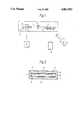
- FIG. 1is a schematic plan view of the device
- FIG. 2is a schematic diagram of a section along the line II--II of one of the liquid crystal cells incorporated in the device of FIG. 1.
- the deviceincludes a number of liquid crystal cells only two such cells 2, 3 being shown in the drawing for the sake of simplicity.
- the cells 2, 3are attached to a framework, indicated as 4, the framework being rotatable about a pivot 5.
- the framework 4 together with the cells 2, 3are located in a temperature controlled enclosure, indicated as 7, each cell 2, 3 being provided with a backing plate 8 held at a required temperature corresponding to the lowest temperature of a thermal image to be synthesized by the device.
- each cell 2, 3comprises a quantity of the smectic A phase liquid crystal 9 known as S2 produced by BDH Chemicals Limited, the crystal 9 being doped to a level of 1% with the dye D16 produced by BDH Chemicals Limited, this dye having an absorption band at a wavelength so as to absorb light in the visible or near infrared wavelength bands.
- the liquid crystal 9is contained between two parallel plates 11, 13 of a material transmissive to light both in the visible or near infrared and the 8-14 ⁇ m wavebands, for example ZnS or ZnSe, the plates having a spacing of between 5 and 50 ⁇ m, separated by spacers 15.
- the inner surfaces of the platesare coated with respective layers 17, 19 of indium tin oxide constituting electrodes for the cell, connections (not shown) and drive circuitry (also not shown) being provided to the electrodes to enable AC voltages to be applied across the liquid crystal 9 as described hereafter.
- a surfactantsuch as lecithin, which causes the liquid crystal at the surfactant liquid crystal interface to adopt a homeotropic alignment.
- the devicefurther includes a laser 25 producing light in the visible or near infrared, and an infrared source 27 producing radiation within the 8-14 ⁇ m wavelength band.
- an RMS voltage greater than a "bulk erase" threshold voltage V be for the particular liquid crystal 9is applied across the liquid crystal within one 2 of the cells, a voltage of this magnitude being effective to cause the crystal 9 to adopt a homeotropic texture in which the optic axes of the molecules of the crystal are normal to the plane of the plates 11, 13 throughout the cell.
- the laser 25is then used to produce a light beam which is scanned across the cell 2, the beam pausing for a short time at desired points within the cell. At these points local heating of the liquid crystal above the isotropic transition temperature takes place, this causing the liquid crystal at these points to adopt a "focal conic" texture in which the optic axes of the molecules of the liquid crystal show rapid spatial variations.
- the laser beammay be moved on to heat another point immediately after the required amount of heat has been absorbed at one point within the liquid crystal, an energy of typically 1nJ ⁇ m 2 being sufficient.
- the laser beammay be used to "write" the cell 2 to produce a pattern of homeotropic and focal conic textures within the liquid crystal across the cell 2, each point within the pattern corresponding to a pixel of the thermal image of the scene which it is required to synthesize.
- the cell 2is rotated on the framework 4 about the pivot 5 to a position away from the laser 25, to a position where the infrared source 27 is able to direct radiation onto the cell as shown in the FIG. 1.
- the crystalIn the areas of the liquid crystal having a homeotropic texture, the crystal is transparent to the infrared radiation. In the areas of the liquid crystal having a focal conic texture however because of the non-zero birefringence of the crystal in these areas the radiation is scattered.
- the thermal imager 29will view a background corresponding to the low temperature of the backing plate 8, while the areas of the liquid crystal having a focal conic texture will scatter photons from the infrared source into the acceptance cone of the detector thus providing an indication of the pattern across the cell 2.
- the output signal of the thermal imager 29may then be inspected to determine the functioning of the imager.
- the thermal imager 29viewing a background held at the lowest temperature of the scene being synthesized, in some circumstances it may be more useful to use a diffuse infrared source representing the highest temperature in the scene, the focal conic texture points within the liquid crystal scattering the photons from the infrared source out of the acceptance cone of the thermal imager 29 to represent pixels of the scene being synthesized which are at lower temperatures.
- the cellsmay be "read" by the infrared beam either by reflection of the beam as shown in FIG. 1, or by transmission of the beam through the cell.
- the form of the infrared "read" beami.e. diffuse or narrow, will generally be determined by the characteristics of the scattering process within the liquid crystal, and also the characteristics of the thermal imaging device being tested.
- the "writing" beammay also take several forms other than the scanned laser beam described herebefore.
- the whole cellmay, for example, be addressed in parallel by projecting the required image onto the cell with an intense optical beam.
- a cinematographic apparatusmay be used, or in the case where the scenes are recorded on a video apparatus, a projection television apparatus may be used.
- each point of the liquid crystal representing a pixel of the scene being synthesizedmay comprise a number of smaller points representing subpixels of the scene, whose size, shape and spacing are designed to achieve the required grey level.
- the distribution of the small points for a given grey levelmay be varied according to a dither algorithm.
- liquid crystalsother than the S2 crystal described herebefore by way of example may be incorporated in a thermal picture synthesizer in accordance with the invention.
- the liquid crystalswill however generally be of the smectic A phase, and usually should have a short nematic or cholesteric phase between the smectic and isotropic phases, although this may be not always be necessary.
- the liquid crystalmay be either a monomeric liquid crystal, or a side-chain polymeric material in which mesogenic groups are attached as side chains to a polymer chain.
- the liquid crystalshould contain cyclohexyl rather than phenyl rings, since cyclohexyl rings have a smaller absorption of infrared radiation in the 8-14 ⁇ m waveband in which most thermal imagers are used.
- the dye used to absorb the light used to "write" the cellmay in some cases be omitted.
- the dyemay also be omitted if the cell incorporates a visible or near infrared absorbing layer between one of the plates and the adjacent surfactant layer.
- each cellcomprises a liquid crystal material confined between two plates which are each transmissive to radiation both in the visible or near infrared and the 8-14 ⁇ m wavebands
- each cellmay alternatively include plates of different materials, one plate being of a material transparent in the visible or near infrared, for example glass, and the other plate being of a material transparent to 8-14 ⁇ m radiation, for example germanium. It will be appreciated that where a germanium plate is used in the cell a conductive electrode layer will be unnecessary on this particular plate. Where the cells do include plates of different materials in this way the visible or near infrared "write" beam and the 8-14 ⁇ m "read” beam will of course be directed onto different sides of the cell.
- the rotating framework 4 described in the above exampleis a particularly simple way of moving the cells relative to the infrared source
- the synthesizermay include a single "cell” in the form of an endless loop which revolves around the "reading" and "writing” beams.
- rotating framework of the device described herebefore by way of examplemay be replaced by one or more moving optical components such as mirrors or mechanical or electronic shutters which enable the cells to be sequentially written and read.
Landscapes
- Physics & Mathematics (AREA)
- Nonlinear Science (AREA)
- Chemical & Material Sciences (AREA)
- Crystallography & Structural Chemistry (AREA)
- General Physics & Mathematics (AREA)
- Optics & Photonics (AREA)
- Liquid Crystal (AREA)
Abstract
Description
Claims (9)
Applications Claiming Priority (2)
| Application Number | Priority Date | Filing Date | Title |
|---|---|---|---|
| GB868606783AGB8606783D0 (en) | 1986-03-19 | 1986-03-19 | Picture synthesizers |
| GB8606783 | 1986-03-19 |
Publications (1)
| Publication Number | Publication Date |
|---|---|
| US4861992Atrue US4861992A (en) | 1989-08-29 |
Family
ID=10594873
Family Applications (1)
| Application Number | Title | Priority Date | Filing Date |
|---|---|---|---|
| US07/124,993Expired - Fee RelatedUS4861992A (en) | 1986-03-19 | 1987-02-27 | Testing of thermal imagers |
Country Status (4)
| Country | Link |
|---|---|
| US (1) | US4861992A (en) |
| EP (1) | EP0261163A1 (en) |
| GB (2) | GB8606783D0 (en) |
| WO (1) | WO1987005713A1 (en) |
Cited By (2)
| Publication number | Priority date | Publication date | Assignee | Title |
|---|---|---|---|---|
| CN100409093C (en)* | 2005-11-25 | 2008-08-06 | 北京科技大学 | Preparation method of intelligent light-shielding film material |
| US20150049941A1 (en)* | 2013-08-19 | 2015-02-19 | Manufacturing Techniques, Inc. (MTEQ) | Electro-Optical System and Method for Analyzing Images of a Scene to Identify the Presence of a Target Color |
Citations (13)
| Publication number | Priority date | Publication date | Assignee | Title |
|---|---|---|---|---|
| US3796999A (en)* | 1972-10-19 | 1974-03-12 | Bell Telephone Labor Inc | Locally erasable thermo-optic smectic liquid crystal storage displays |
| US4040047A (en)* | 1974-06-14 | 1977-08-02 | Thomson-Csf | Erasable thermo-optic storage display of a transmitted image |
| US4059340A (en)* | 1974-11-18 | 1977-11-22 | Bell Telephone Laboratories, Incorporated | Doped liquid crystal display device |
| GB1536568A (en)* | 1974-12-24 | 1978-12-20 | Thomson Csf | Thermo-optic smectic liquid-crystal storage display |
| US4263515A (en)* | 1978-07-20 | 1981-04-21 | Barr & Stroud Limited | Variable temperature test target |
| EP0087477A1 (en)* | 1981-09-07 | 1983-09-07 | Sony Corporation | Liquid crystal display device |
| GB2140023A (en)* | 1983-04-26 | 1984-11-21 | Sony Corp | Liquid crystal display devices |
| GB2161951A (en)* | 1984-07-17 | 1986-01-22 | Stc Plc | Laser addressed smectic displays |
| GB2162333A (en)* | 1984-07-20 | 1986-01-29 | Stc Plc | Recording spatially modulated light patterns |
| GB2162715A (en)* | 1984-08-02 | 1986-02-05 | Stc Plc | Thermal imaging system |
| US4639722A (en)* | 1981-11-20 | 1987-01-27 | Sony Corporation | Liquid crystal display apparatus |
| US4659502A (en)* | 1984-01-17 | 1987-04-21 | Merck Patent Gesellschaft Mit Beschrankter Haftung | Ethane derivatives |
| US4693557A (en)* | 1984-03-02 | 1987-09-15 | Manchester R & D Partnership | Liquid crystal motion picture projector |
- 1986
- 1986-03-19GBGB868606783Apatent/GB8606783D0/enactivePending
- 1987
- 1987-02-27GBGB8704675Apatent/GB2188743B/ennot_activeExpired
- 1987-02-27WOPCT/GB1987/000140patent/WO1987005713A1/ennot_activeApplication Discontinuation
- 1987-02-27USUS07/124,993patent/US4861992A/ennot_activeExpired - Fee Related
- 1987-02-27EPEP87901559Apatent/EP0261163A1/ennot_activeWithdrawn
Patent Citations (13)
| Publication number | Priority date | Publication date | Assignee | Title |
|---|---|---|---|---|
| US3796999A (en)* | 1972-10-19 | 1974-03-12 | Bell Telephone Labor Inc | Locally erasable thermo-optic smectic liquid crystal storage displays |
| US4040047A (en)* | 1974-06-14 | 1977-08-02 | Thomson-Csf | Erasable thermo-optic storage display of a transmitted image |
| US4059340A (en)* | 1974-11-18 | 1977-11-22 | Bell Telephone Laboratories, Incorporated | Doped liquid crystal display device |
| GB1536568A (en)* | 1974-12-24 | 1978-12-20 | Thomson Csf | Thermo-optic smectic liquid-crystal storage display |
| US4263515A (en)* | 1978-07-20 | 1981-04-21 | Barr & Stroud Limited | Variable temperature test target |
| EP0087477A1 (en)* | 1981-09-07 | 1983-09-07 | Sony Corporation | Liquid crystal display device |
| US4639722A (en)* | 1981-11-20 | 1987-01-27 | Sony Corporation | Liquid crystal display apparatus |
| GB2140023A (en)* | 1983-04-26 | 1984-11-21 | Sony Corp | Liquid crystal display devices |
| US4659502A (en)* | 1984-01-17 | 1987-04-21 | Merck Patent Gesellschaft Mit Beschrankter Haftung | Ethane derivatives |
| US4693557A (en)* | 1984-03-02 | 1987-09-15 | Manchester R & D Partnership | Liquid crystal motion picture projector |
| GB2161951A (en)* | 1984-07-17 | 1986-01-22 | Stc Plc | Laser addressed smectic displays |
| GB2162333A (en)* | 1984-07-20 | 1986-01-29 | Stc Plc | Recording spatially modulated light patterns |
| GB2162715A (en)* | 1984-08-02 | 1986-02-05 | Stc Plc | Thermal imaging system |
Non-Patent Citations (4)
| Title |
|---|
| APIE vol. 98, Assessment of Imaging Systems (Sira Nov. 1976 London), "The Laboratory Evaluation of Thermal Imaging Systems", by A. R. Newbery & R. Worswick, pp. 96-104. |
| APIE vol. 98, Assessment of Imaging Systems (Sira Nov. 1976 London), The Laboratory Evaluation of Thermal Imaging Systems , by A. R. Newbery & R. Worswick, pp. 96 104.* |
| Appl. Phys. Lett., vol. 22, No. 3, 1 Feb. 1973, "Ir-Laser-Addressed Thermo-Optic Smectic Liquid-Crystal Storage Displays", by Frederick J. Kahn, pp. 111-113. |
| Appl. Phys. Lett., vol. 22, No. 3, 1 Feb. 1973, Ir Laser Addressed Thermo Optic Smectic Liquid Crystal Storage Displays , by Frederick J. Kahn, pp. 111 113.* |
Cited By (3)
| Publication number | Priority date | Publication date | Assignee | Title |
|---|---|---|---|---|
| CN100409093C (en)* | 2005-11-25 | 2008-08-06 | 北京科技大学 | Preparation method of intelligent light-shielding film material |
| US20150049941A1 (en)* | 2013-08-19 | 2015-02-19 | Manufacturing Techniques, Inc. (MTEQ) | Electro-Optical System and Method for Analyzing Images of a Scene to Identify the Presence of a Target Color |
| US9196056B2 (en)* | 2013-08-19 | 2015-11-24 | Manufacturing Techniques, Inc. | Electro-optical system and method for analyzing images of a scene to identify the presence of a target color |
Also Published As
| Publication number | Publication date |
|---|---|
| EP0261163A1 (en) | 1988-03-30 |
| WO1987005713A1 (en) | 1987-09-24 |
| GB2188743A (en) | 1987-10-07 |
| GB8704675D0 (en) | 1987-04-01 |
| GB2188743B (en) | 1989-11-29 |
| GB8606783D0 (en) | 1986-04-23 |
Similar Documents
| Publication | Publication Date | Title |
|---|---|---|
| KR970001733B1 (en) | LCD Video Projector with Memory Function | |
| US3592527A (en) | Image display device | |
| US4679910A (en) | Dual liquid-crystal cell-based visible-to-infrared dynamic image converter | |
| US4751509A (en) | Light valve for use in a color display unit with a diffraction grating assembly included in the valve | |
| US4040047A (en) | Erasable thermo-optic storage display of a transmitted image | |
| US4196974A (en) | Smectic liquid crystal display cell | |
| US4699498A (en) | Image projector with liquid crystal light shutter | |
| US4288822A (en) | System for the analysis and the recording of monochromic images | |
| US4368386A (en) | Liquid-crystal image converter device | |
| US5140448A (en) | Apparatus for and method of operation of smectic liquid crystal light valve having scattering centers | |
| US4861992A (en) | Testing of thermal imagers | |
| US4530010A (en) | Dynamic infrared scene projector | |
| US5016984A (en) | Liquid crystal motion picture projector with memory | |
| Pritchard | Dynamic IR scene generation: basic requirements and comparative display device design | |
| US5159456A (en) | Photo-to-photo transducer and method of operation using a photo-moldulation member affected by a change distribution in a photoconductive member and a voltage applied across electrodes | |
| US5061041A (en) | Liquid crystal motion picture projector with memory | |
| US4828366A (en) | Laser-addressable liquid crystal cell having mark positioning layer | |
| JPH0548883B2 (en) | ||
| EP0425321A2 (en) | Liquid crystal cells and their use for recording information or for projecting an image | |
| JPS60165626A (en) | Thermal writing type liquid crystal display device | |
| Jutamulia et al. | Infrared signal processing using a liquid crystal television | |
| JP2877884B2 (en) | Photothermal writing type spatial light modulator | |
| EP0657764B1 (en) | Photo-to-photo transducer | |
| JPS60107618A (en) | Positive display device of liquid crystal light valve | |
| JPH02125767A (en) | Digital image output apparatus |
Legal Events
| Date | Code | Title | Description |
|---|---|---|---|
| AS | Assignment | Owner name:GENERAL ELECTRIC COMPANY, P.L.C., THE, 1 STANHOPE Free format text:ASSIGNMENT OF ASSIGNORS INTEREST.;ASSIGNOR:CLARK, MICHAEL G.;REEL/FRAME:004855/0316 Effective date:19880204 Owner name:GENERAL ELECTRIC COMPANY, P.L.C., THE, A BRITISH C Free format text:ASSIGNMENT OF ASSIGNORS INTEREST;ASSIGNOR:CLARK, MICHAEL G.;REEL/FRAME:004855/0316 Effective date:19880204 | |
| AS | Assignment | Owner name:GENERAL ELECTRIC COMPANY, P.L.C., THE, 1 STANHOPE Free format text:ASSIGNMENT OF ASSIGNORS INTEREST.;ASSIGNOR:WILTSHIRE, MICHAEL C.;REEL/FRAME:004855/0320 Effective date:19880217 Owner name:GENERAL ELECTRIC COMPANY, P.L.C., THE, A BRITISH C Free format text:ASSIGNMENT OF ASSIGNORS INTEREST;ASSIGNOR:WILTSHIRE, MICHAEL C.;REEL/FRAME:004855/0320 Effective date:19880217 | |
| FEPP | Fee payment procedure | Free format text:PAYOR NUMBER ASSIGNED (ORIGINAL EVENT CODE: ASPN); ENTITY STATUS OF PATENT OWNER: LARGE ENTITY | |
| REMI | Maintenance fee reminder mailed | ||
| LAPS | Lapse for failure to pay maintenance fees | ||
| FP | Lapsed due to failure to pay maintenance fee | Effective date:19930829 | |
| STCH | Information on status: patent discontinuation | Free format text:PATENT EXPIRED DUE TO NONPAYMENT OF MAINTENANCE FEES UNDER 37 CFR 1.362 |