US4859989A - Security system and signal carrying member thereof - Google Patents
Security system and signal carrying member thereofDownload PDFInfo
- Publication number
- US4859989A US4859989AUS07/126,670US12667087AUS4859989AUS 4859989 AUS4859989 AUS 4859989AUS 12667087 AUS12667087 AUS 12667087AUS 4859989 AUS4859989 AUS 4859989A
- Authority
- US
- United States
- Prior art keywords
- semi
- conductive
- signal
- layer
- tape
- Prior art date
- Legal status (The legal status is an assumption and is not a legal conclusion. Google has not performed a legal analysis and makes no representation as to the accuracy of the status listed.)
- Expired - Fee Related
Links
- 238000004804windingMethods0.000claims5
- 229920001343polytetrafluoroethylenePolymers0.000abstractdescription6
- 239000004810polytetrafluoroethyleneSubstances0.000abstractdescription6
- 239000002657fibrous materialSubstances0.000abstractdescription2
- 239000000835fiberSubstances0.000abstract1
- 239000010410layerSubstances0.000description95
- 238000001514detection methodMethods0.000description14
- 238000010276constructionMethods0.000description6
- 238000013461designMethods0.000description5
- 239000000853adhesiveSubstances0.000description4
- 230000001070adhesive effectEffects0.000description4
- 238000010586diagramMethods0.000description4
- 239000000463materialSubstances0.000description4
- 239000004020conductorSubstances0.000description3
- 238000001125extrusionMethods0.000description3
- 238000009413insulationMethods0.000description3
- 238000000034methodMethods0.000description3
- 238000012986modificationMethods0.000description3
- 230000004048modificationEffects0.000description3
- 230000035515penetrationEffects0.000description3
- RYGMFSIKBFXOCR-UHFFFAOYSA-NCopperChemical compound[Cu]RYGMFSIKBFXOCR-UHFFFAOYSA-N0.000description2
- 239000004831Hot glueSubstances0.000description2
- 239000011248coating agentSubstances0.000description2
- 238000000576coating methodMethods0.000description2
- 238000005520cutting processMethods0.000description2
- 229920000728polyesterPolymers0.000description2
- 229920006267polyester filmPolymers0.000description2
- 230000001681protective effectEffects0.000description2
- 229920001169thermoplasticPolymers0.000description2
- 239000004416thermosoftening plasticSubstances0.000description2
- OKTJSMMVPCPJKN-UHFFFAOYSA-NCarbonChemical compound[C]OKTJSMMVPCPJKN-UHFFFAOYSA-N0.000description1
- 229910052799carbonInorganic materials0.000description1
- 229910052802copperInorganic materials0.000description1
- 239000010949copperSubstances0.000description1
- 239000012530fluidSubstances0.000description1
- 239000012634fragmentSubstances0.000description1
- 238000010348incorporationMethods0.000description1
- 239000011810insulating materialSubstances0.000description1
- 238000004519manufacturing processMethods0.000description1
- 238000005259measurementMethods0.000description1
- 239000002184metalSubstances0.000description1
- 229910052751metalInorganic materials0.000description1
- 230000003287optical effectEffects0.000description1
- 239000004033plasticSubstances0.000description1
- 229920003023plasticPolymers0.000description1
- -1polytetrafluoroethylenePolymers0.000description1
- 229920002635polyurethanePolymers0.000description1
- 239000004814polyurethaneSubstances0.000description1
- 230000000717retained effectEffects0.000description1
- 238000005096rolling processMethods0.000description1
- 238000010079rubber tappingMethods0.000description1
- 239000000523sampleSubstances0.000description1
- 239000002356single layerSubstances0.000description1
- 239000012815thermoplastic materialSubstances0.000description1
- 238000012546transferMethods0.000description1
Images


Classifications
- G—PHYSICS
- G08—SIGNALLING
- G08B—SIGNALLING OR CALLING SYSTEMS; ORDER TELEGRAPHS; ALARM SYSTEMS
- G08B13/00—Burglar, theft or intruder alarms
- G08B13/02—Mechanical actuation
- G08B13/12—Mechanical actuation by the breaking or disturbance of stretched cords or wires
- G08B13/126—Mechanical actuation by the breaking or disturbance of stretched cords or wires for a housing, e.g. a box, a safe, or a room
- G08B13/128—Mechanical actuation by the breaking or disturbance of stretched cords or wires for a housing, e.g. a box, a safe, or a room the housing being an electronic circuit unit, e.g. memory or CPU chip
- G—PHYSICS
- G01—MEASURING; TESTING
- G01R—MEASURING ELECTRIC VARIABLES; MEASURING MAGNETIC VARIABLES
- G01R31/00—Arrangements for testing electric properties; Arrangements for locating electric faults; Arrangements for electrical testing characterised by what is being tested not provided for elsewhere
- G01R31/50—Testing of electric apparatus, lines, cables or components for short-circuits, continuity, leakage current or incorrect line connections
- G01R31/58—Testing of lines, cables or conductors
- H—ELECTRICITY
- H01—ELECTRIC ELEMENTS
- H01B—CABLES; CONDUCTORS; INSULATORS; SELECTION OF MATERIALS FOR THEIR CONDUCTIVE, INSULATING OR DIELECTRIC PROPERTIES
- H01B7/00—Insulated conductors or cables characterised by their form
- H01B7/32—Insulated conductors or cables characterised by their form with arrangements for indicating defects, e.g. breaks or leaks
- H01B7/328—Insulated conductors or cables characterised by their form with arrangements for indicating defects, e.g. breaks or leaks comprising violation sensing means
Definitions
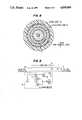
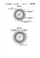
- the semi-conductive layer and the insulation layerare both formed to tape which is wrapped helically around the core to 0.95 wraps, i.e. with a gap of 5% or thereabouts between turns to prevent overlap.
- wrappingis the preferred method.
- the protective sheathis conveniently a 0.5 mm PVC coating applied by extrusion.
Landscapes
- Physics & Mathematics (AREA)
- General Physics & Mathematics (AREA)
- Engineering & Computer Science (AREA)
- Computer Hardware Design (AREA)
- General Engineering & Computer Science (AREA)
- Burglar Alarm Systems (AREA)
Abstract
Description
Claims (11)
Priority Applications (1)
| Application Number | Priority Date | Filing Date | Title |
|---|---|---|---|
| US07/126,670US4859989A (en) | 1987-12-01 | 1987-12-01 | Security system and signal carrying member thereof |
Applications Claiming Priority (1)
| Application Number | Priority Date | Filing Date | Title |
|---|---|---|---|
| US07/126,670US4859989A (en) | 1987-12-01 | 1987-12-01 | Security system and signal carrying member thereof |
Publications (1)
| Publication Number | Publication Date |
|---|---|
| US4859989Atrue US4859989A (en) | 1989-08-22 |
Family
ID=22426115
Family Applications (1)
| Application Number | Title | Priority Date | Filing Date |
|---|---|---|---|
| US07/126,670Expired - Fee RelatedUS4859989A (en) | 1987-12-01 | 1987-12-01 | Security system and signal carrying member thereof |
Country Status (1)
| Country | Link |
|---|---|
| US (1) | US4859989A (en) |
Cited By (91)
| Publication number | Priority date | Publication date | Assignee | Title |
|---|---|---|---|---|
| US4972175A (en)* | 1988-06-17 | 1990-11-20 | Macpherson Hugh | Security enclosures |
| US4988949A (en)* | 1989-05-15 | 1991-01-29 | Westinghouse Electric Corp. | Apparatus for detecting excessive chafing of a cable arrangement against an electrically grounded structure |
| US5017908A (en)* | 1989-04-04 | 1991-05-21 | Macpherson Hugh | Solvent responsive signal-carrying device |
| EP0459838A3 (en)* | 1990-06-01 | 1992-08-12 | W.L. Gore & Associates (Uk) Ltd | Flexible sheeting |
| EP0524003A1 (en)* | 1991-07-19 | 1993-01-20 | W.L. GORE & ASSOCIATES (UK) LTD | Protective sheath |
| US5334971A (en)* | 1992-09-08 | 1994-08-02 | Modsec Systems (Proprietary) Limited | Security device kit, a security device and a security installation |
| US5339038A (en)* | 1992-07-06 | 1994-08-16 | Westinghouse Electric Corporation | Assembly for detecting and locating cable pinching |
| WO1997021085A3 (en)* | 1995-11-10 | 1997-09-12 | Dietz Kabeltechnik | Electric monitoring of cables and the like for detecting damages thereof |
| US6020811A (en)* | 1995-02-21 | 2000-02-01 | Hitachi, Ltd. | Apparatus for multiplexing between on-board units in a vehicle |
| US6261437B1 (en) | 1996-11-04 | 2001-07-17 | Asea Brown Boveri Ab | Anode, process for anodizing, anodized wire and electric device comprising such anodized wire |
| US6279850B1 (en) | 1996-11-04 | 2001-08-28 | Abb Ab | Cable forerunner |
| US6357688B1 (en) | 1997-02-03 | 2002-03-19 | Abb Ab | Coiling device |
| WO2002027734A1 (en)* | 2000-09-27 | 2002-04-04 | Donald Graeme Chalmers | Electrical cabling system for high voltage networks |
| US6369470B1 (en) | 1996-11-04 | 2002-04-09 | Abb Ab | Axial cooling of a rotor |
| US6376775B1 (en) | 1996-05-29 | 2002-04-23 | Abb Ab | Conductor for high-voltage windings and a rotating electric machine comprising a winding including the conductor |
| US20020047439A1 (en)* | 1996-05-29 | 2002-04-25 | Mats Leijon | High voltage ac machine winding with grounded neutral circuit |
| US6396187B1 (en) | 1996-11-04 | 2002-05-28 | Asea Brown Boveri Ab | Laminated magnetic core for electric machines |
| US6417456B1 (en)* | 1996-05-29 | 2002-07-09 | Abb Ab | Insulated conductor for high-voltage windings and a method of manufacturing the same |
| JP3308542B2 (en) | 1995-02-21 | 2002-07-29 | 株式会社 日立製作所 | Vehicle power supply device, vehicle power control method, power supply relay circuit used in vehicle power control device, vehicle integrated wiring device, control unit used in vehicle integrated wiring device |
| US6429563B1 (en) | 1997-02-03 | 2002-08-06 | Abb Ab | Mounting device for rotating electric machines |
| US6439497B1 (en) | 1997-02-03 | 2002-08-27 | Abb Ab | Method and device for mounting a winding |
| US6465979B1 (en) | 1997-02-03 | 2002-10-15 | Abb Ab | Series compensation of electric alternating current machines |
| US6525504B1 (en) | 1997-11-28 | 2003-02-25 | Abb Ab | Method and device for controlling the magnetic flux in a rotating high voltage electric alternating current machine |
| US6646363B2 (en) | 1997-02-03 | 2003-11-11 | Abb Ab | Rotating electric machine with coil supports |
| US6801421B1 (en) | 1998-09-29 | 2004-10-05 | Abb Ab | Switchable flux control for high power static electromagnetic devices |
| US6822363B2 (en) | 1996-05-29 | 2004-11-23 | Abb Ab | Electromagnetic device |
| US6825585B1 (en) | 1997-02-03 | 2004-11-30 | Abb Ab | End plate |
| US6831388B1 (en) | 1996-05-29 | 2004-12-14 | Abb Ab | Synchronous compensator plant |
| US6873080B1 (en) | 1997-09-30 | 2005-03-29 | Abb Ab | Synchronous compensator plant |
| US6885273B2 (en) | 2000-03-30 | 2005-04-26 | Abb Ab | Induction devices with distributed air gaps |
| US20050099258A1 (en)* | 1997-02-03 | 2005-05-12 | Asea Brown Boveri Ab | Power transformer/inductor |
| US20050104610A1 (en)* | 2002-11-08 | 2005-05-19 | Timothy Lesher | Probe station with low noise characteristics |
| US6970063B1 (en) | 1997-02-03 | 2005-11-29 | Abb Ab | Power transformer/inductor |
| US6972505B1 (en) | 1996-05-29 | 2005-12-06 | Abb | Rotating electrical machine having high-voltage stator winding and elongated support devices supporting the winding and method for manufacturing the same |
| US6995646B1 (en) | 1997-02-03 | 2006-02-07 | Abb Ab | Transformer with voltage regulating means |
| US7019429B1 (en) | 1997-11-27 | 2006-03-28 | Asea Brown Boveri Ab | Method of applying a tube member in a stator slot in a rotating electrical machine |
| US7045704B2 (en) | 2000-04-28 | 2006-05-16 | Abb Ab | Stationary induction machine and a cable therefor |
| US7061133B1 (en) | 1997-11-28 | 2006-06-13 | Abb Ab | Wind power plant |
| US7138813B2 (en) | 1999-06-30 | 2006-11-21 | Cascade Microtech, Inc. | Probe station thermal chuck with shielding for capacitive current |
| US7141908B2 (en) | 2000-03-01 | 2006-11-28 | Abb Ab | Rotating electrical machine |
| US7164279B2 (en) | 1995-04-14 | 2007-01-16 | Cascade Microtech, Inc. | System for evaluating probing networks |
| US7176705B2 (en) | 2004-06-07 | 2007-02-13 | Cascade Microtech, Inc. | Thermal optical chuck |
| US7187188B2 (en) | 2003-12-24 | 2007-03-06 | Cascade Microtech, Inc. | Chuck with integrated wafer support |
| US7190181B2 (en) | 1997-06-06 | 2007-03-13 | Cascade Microtech, Inc. | Probe station having multiple enclosures |
| US7221172B2 (en) | 2003-05-06 | 2007-05-22 | Cascade Microtech, Inc. | Switched suspended conductor and connection |
| US7221146B2 (en) | 2002-12-13 | 2007-05-22 | Cascade Microtech, Inc. | Guarded tub enclosure |
| US7250626B2 (en) | 2003-10-22 | 2007-07-31 | Cascade Microtech, Inc. | Probe testing structure |
| US7250779B2 (en) | 2002-11-25 | 2007-07-31 | Cascade Microtech, Inc. | Probe station with low inductance path |
| US7268533B2 (en) | 2001-08-31 | 2007-09-11 | Cascade Microtech, Inc. | Optical testing device |
| US7304488B2 (en) | 2002-05-23 | 2007-12-04 | Cascade Microtech, Inc. | Shielded probe for high-frequency testing of a device under test |
| US7330023B2 (en) | 1992-06-11 | 2008-02-12 | Cascade Microtech, Inc. | Wafer probe station having a skirting component |
| US7330041B2 (en) | 2004-06-14 | 2008-02-12 | Cascade Microtech, Inc. | Localizing a temperature of a device for testing |
| US7348787B2 (en) | 1992-06-11 | 2008-03-25 | Cascade Microtech, Inc. | Wafer probe station having environment control enclosure |
| US7352168B2 (en) | 2000-09-05 | 2008-04-01 | Cascade Microtech, Inc. | Chuck for holding a device under test |
| US7355420B2 (en) | 2001-08-21 | 2008-04-08 | Cascade Microtech, Inc. | Membrane probing system |
| US20080084268A1 (en)* | 2006-10-09 | 2008-04-10 | Weishe Zhang | Unrecoverable line-type temperature sensitive detector having short-circuit fault alarm function |
| US7368927B2 (en) | 2004-07-07 | 2008-05-06 | Cascade Microtech, Inc. | Probe head having a membrane suspended probe |
| US7368925B2 (en) | 2002-01-25 | 2008-05-06 | Cascade Microtech, Inc. | Probe station with two platens |
| US7403028B2 (en) | 2006-06-12 | 2008-07-22 | Cascade Microtech, Inc. | Test structure and probe for differential signals |
| US7403025B2 (en) | 2000-02-25 | 2008-07-22 | Cascade Microtech, Inc. | Membrane probing system |
| US7417446B2 (en) | 2002-11-13 | 2008-08-26 | Cascade Microtech, Inc. | Probe for combined signals |
| US7420381B2 (en) | 2004-09-13 | 2008-09-02 | Cascade Microtech, Inc. | Double sided probing structures |
| US7443186B2 (en) | 2006-06-12 | 2008-10-28 | Cascade Microtech, Inc. | On-wafer test structures for differential signals |
| US7449899B2 (en) | 2005-06-08 | 2008-11-11 | Cascade Microtech, Inc. | Probe for high frequency signals |
| US7456646B2 (en) | 2000-12-04 | 2008-11-25 | Cascade Microtech, Inc. | Wafer probe |
| US7492172B2 (en) | 2003-05-23 | 2009-02-17 | Cascade Microtech, Inc. | Chuck for holding a device under test |
| US7498829B2 (en) | 2003-05-23 | 2009-03-03 | Cascade Microtech, Inc. | Shielded probe for testing a device under test |
| US7504842B2 (en) | 1997-05-28 | 2009-03-17 | Cascade Microtech, Inc. | Probe holder for testing of a test device |
| US7535247B2 (en) | 2005-01-31 | 2009-05-19 | Cascade Microtech, Inc. | Interface for testing semiconductors |
| US7533462B2 (en) | 1999-06-04 | 2009-05-19 | Cascade Microtech, Inc. | Method of constructing a membrane probe |
| US7541821B2 (en) | 1996-08-08 | 2009-06-02 | Cascade Microtech, Inc. | Membrane probing system with local contact scrub |
| US7554322B2 (en) | 2000-09-05 | 2009-06-30 | Cascade Microtech, Inc. | Probe station |
| US7609077B2 (en) | 2006-06-09 | 2009-10-27 | Cascade Microtech, Inc. | Differential signal probe with integral balun |
| US7619419B2 (en) | 2005-06-13 | 2009-11-17 | Cascade Microtech, Inc. | Wideband active-passive differential signal probe |
| US7656172B2 (en) | 2005-01-31 | 2010-02-02 | Cascade Microtech, Inc. | System for testing semiconductors |
| US7681312B2 (en) | 1998-07-14 | 2010-03-23 | Cascade Microtech, Inc. | Membrane probing system |
| US7723999B2 (en) | 2006-06-12 | 2010-05-25 | Cascade Microtech, Inc. | Calibration structures for differential signal probing |
| US7759953B2 (en) | 2003-12-24 | 2010-07-20 | Cascade Microtech, Inc. | Active wafer probe |
| US7764072B2 (en) | 2006-06-12 | 2010-07-27 | Cascade Microtech, Inc. | Differential signal probing system |
| US7876114B2 (en) | 2007-08-08 | 2011-01-25 | Cascade Microtech, Inc. | Differential waveguide probe |
| US7888957B2 (en) | 2008-10-06 | 2011-02-15 | Cascade Microtech, Inc. | Probing apparatus with impedance optimized interface |
| US8319503B2 (en) | 2008-11-24 | 2012-11-27 | Cascade Microtech, Inc. | Test apparatus for measuring a characteristic of a device under test |
| US8410806B2 (en) | 2008-11-21 | 2013-04-02 | Cascade Microtech, Inc. | Replaceable coupon for a probing apparatus |
| US20130335102A1 (en)* | 2012-06-15 | 2013-12-19 | Tyco Electronics Uk Ltd. | Secure jacket |
| US20140303470A1 (en)* | 2011-11-17 | 2014-10-09 | Nippon Telegraph And Telegraph And Telephone Corporation | Conductive polymer fibers, method and device for producing conductive polymer fibers, biological electrode, device for measuring biological signals, implantable electrode, and device for measuring biological signals |
| JP2015025733A (en)* | 2013-07-26 | 2015-02-05 | 矢崎エナジーシステム株式会社 | Cable |
| US20160282216A1 (en)* | 2015-03-26 | 2016-09-29 | Flownix Co., Ltd. | Leak sensor for side detection |
| CN109154705A (en)* | 2016-03-03 | 2019-01-04 | 北德海底电缆有限公司 | Submarine communication cable and method and apparatus for manufacturing submarine communication cable |
| US20190250357A1 (en)* | 2017-07-12 | 2019-08-15 | Zhongtian Power Optical Cable Co., Ltd. | Hybrid cable and manufacturing method |
| EP3564690A1 (en)* | 2018-05-03 | 2019-11-06 | ETH Zurich | A cable assembly |
| CN111863334A (en)* | 2020-08-01 | 2020-10-30 | 江苏江扬特种电缆有限公司 | High-safety communication cable and using method thereof |
Citations (9)
| Publication number | Priority date | Publication date | Assignee | Title |
|---|---|---|---|---|
| US2581213A (en)* | 1949-12-15 | 1952-01-01 | Gen Electric | Temperature responsive signaling and locating system |
| US2691698A (en)* | 1950-10-26 | 1954-10-12 | Res Products Inc | Security telephone cable with jammer and alarm |
| US3633194A (en)* | 1962-09-26 | 1972-01-04 | Anoconda Wire And Cable Co | Tamperproof barrier |
| US3748369A (en)* | 1971-03-08 | 1973-07-24 | Gen Cable Corp | Method of shielding high voltage solid dielectric power cables |
| US3750127A (en)* | 1971-10-28 | 1973-07-31 | Gen Dynamics Corp | Method and means for sensing strain with a piezoelectric strain sensing element |
| US3763482A (en)* | 1971-02-01 | 1973-10-02 | Gte Sylvania Inc | Coaxial cable transducer |
| US4155083A (en)* | 1976-02-19 | 1979-05-15 | N. V. Bekaert S. A. | Composite wire and fence made therefrom useful for security purposes |
| US4450434A (en)* | 1981-05-19 | 1984-05-22 | The United States Of America As Represented By The Secretary Of The Army | Apparatus for determining break locations in fencing |
| US4453159A (en)* | 1981-09-28 | 1984-06-05 | Thermon Manufacturing Company | Self-monitoring heat tracing system |
- 1987
- 1987-12-01USUS07/126,670patent/US4859989A/ennot_activeExpired - Fee Related
Patent Citations (9)
| Publication number | Priority date | Publication date | Assignee | Title |
|---|---|---|---|---|
| US2581213A (en)* | 1949-12-15 | 1952-01-01 | Gen Electric | Temperature responsive signaling and locating system |
| US2691698A (en)* | 1950-10-26 | 1954-10-12 | Res Products Inc | Security telephone cable with jammer and alarm |
| US3633194A (en)* | 1962-09-26 | 1972-01-04 | Anoconda Wire And Cable Co | Tamperproof barrier |
| US3763482A (en)* | 1971-02-01 | 1973-10-02 | Gte Sylvania Inc | Coaxial cable transducer |
| US3748369A (en)* | 1971-03-08 | 1973-07-24 | Gen Cable Corp | Method of shielding high voltage solid dielectric power cables |
| US3750127A (en)* | 1971-10-28 | 1973-07-31 | Gen Dynamics Corp | Method and means for sensing strain with a piezoelectric strain sensing element |
| US4155083A (en)* | 1976-02-19 | 1979-05-15 | N. V. Bekaert S. A. | Composite wire and fence made therefrom useful for security purposes |
| US4450434A (en)* | 1981-05-19 | 1984-05-22 | The United States Of America As Represented By The Secretary Of The Army | Apparatus for determining break locations in fencing |
| US4453159A (en)* | 1981-09-28 | 1984-06-05 | Thermon Manufacturing Company | Self-monitoring heat tracing system |
Cited By (156)
| Publication number | Priority date | Publication date | Assignee | Title |
|---|---|---|---|---|
| US4972175A (en)* | 1988-06-17 | 1990-11-20 | Macpherson Hugh | Security enclosures |
| US5017908A (en)* | 1989-04-04 | 1991-05-21 | Macpherson Hugh | Solvent responsive signal-carrying device |
| US4988949A (en)* | 1989-05-15 | 1991-01-29 | Westinghouse Electric Corp. | Apparatus for detecting excessive chafing of a cable arrangement against an electrically grounded structure |
| EP0459838A3 (en)* | 1990-06-01 | 1992-08-12 | W.L. Gore & Associates (Uk) Ltd | Flexible sheeting |
| US5438474A (en)* | 1991-07-19 | 1995-08-01 | W. L. Gore & Associates (Uk) Ltd. | Protective sheath |
| EP0524003A1 (en)* | 1991-07-19 | 1993-01-20 | W.L. GORE & ASSOCIATES (UK) LTD | Protective sheath |
| US7595632B2 (en) | 1992-06-11 | 2009-09-29 | Cascade Microtech, Inc. | Wafer probe station having environment control enclosure |
| US7348787B2 (en) | 1992-06-11 | 2008-03-25 | Cascade Microtech, Inc. | Wafer probe station having environment control enclosure |
| US7589518B2 (en) | 1992-06-11 | 2009-09-15 | Cascade Microtech, Inc. | Wafer probe station having a skirting component |
| US7492147B2 (en) | 1992-06-11 | 2009-02-17 | Cascade Microtech, Inc. | Wafer probe station having a skirting component |
| US7330023B2 (en) | 1992-06-11 | 2008-02-12 | Cascade Microtech, Inc. | Wafer probe station having a skirting component |
| US5339038A (en)* | 1992-07-06 | 1994-08-16 | Westinghouse Electric Corporation | Assembly for detecting and locating cable pinching |
| US5334971A (en)* | 1992-09-08 | 1994-08-02 | Modsec Systems (Proprietary) Limited | Security device kit, a security device and a security installation |
| US6020811A (en)* | 1995-02-21 | 2000-02-01 | Hitachi, Ltd. | Apparatus for multiplexing between on-board units in a vehicle |
| US6243018B1 (en)* | 1995-02-21 | 2001-06-05 | Hitachi, Ltd. | Apparatus for multiplexing between on-board units in a vehicle |
| JP3308542B2 (en) | 1995-02-21 | 2002-07-29 | 株式会社 日立製作所 | Vehicle power supply device, vehicle power control method, power supply relay circuit used in vehicle power control device, vehicle integrated wiring device, control unit used in vehicle integrated wiring device |
| US7164279B2 (en) | 1995-04-14 | 2007-01-16 | Cascade Microtech, Inc. | System for evaluating probing networks |
| US7321233B2 (en) | 1995-04-14 | 2008-01-22 | Cascade Microtech, Inc. | System for evaluating probing networks |
| WO1997021085A3 (en)* | 1995-11-10 | 1997-09-12 | Dietz Kabeltechnik | Electric monitoring of cables and the like for detecting damages thereof |
| US6822363B2 (en) | 1996-05-29 | 2004-11-23 | Abb Ab | Electromagnetic device |
| US6940380B1 (en) | 1996-05-29 | 2005-09-06 | Abb Ab | Transformer/reactor |
| US6906447B2 (en) | 1996-05-29 | 2005-06-14 | Abb Ab | Rotating asynchronous converter and a generator device |
| US20020047439A1 (en)* | 1996-05-29 | 2002-04-25 | Mats Leijon | High voltage ac machine winding with grounded neutral circuit |
| US6376775B1 (en) | 1996-05-29 | 2002-04-23 | Abb Ab | Conductor for high-voltage windings and a rotating electric machine comprising a winding including the conductor |
| US6417456B1 (en)* | 1996-05-29 | 2002-07-09 | Abb Ab | Insulated conductor for high-voltage windings and a method of manufacturing the same |
| US6894416B1 (en) | 1996-05-29 | 2005-05-17 | Abb Ab | Hydro-generator plant |
| US6936947B1 (en) | 1996-05-29 | 2005-08-30 | Abb Ab | Turbo generator plant with a high voltage electric generator |
| US6919664B2 (en) | 1996-05-29 | 2005-07-19 | Abb Ab | High voltage plants with electric motors |
| US6891303B2 (en) | 1996-05-29 | 2005-05-10 | Abb Ab | High voltage AC machine winding with grounded neutral circuit |
| US6831388B1 (en) | 1996-05-29 | 2004-12-14 | Abb Ab | Synchronous compensator plant |
| US6972505B1 (en) | 1996-05-29 | 2005-12-06 | Abb | Rotating electrical machine having high-voltage stator winding and elongated support devices supporting the winding and method for manufacturing the same |
| US7541821B2 (en) | 1996-08-08 | 2009-06-02 | Cascade Microtech, Inc. | Membrane probing system with local contact scrub |
| US7893704B2 (en) | 1996-08-08 | 2011-02-22 | Cascade Microtech, Inc. | Membrane probing structure with laterally scrubbing contacts |
| US6261437B1 (en) | 1996-11-04 | 2001-07-17 | Asea Brown Boveri Ab | Anode, process for anodizing, anodized wire and electric device comprising such anodized wire |
| US6279850B1 (en) | 1996-11-04 | 2001-08-28 | Abb Ab | Cable forerunner |
| US6369470B1 (en) | 1996-11-04 | 2002-04-09 | Abb Ab | Axial cooling of a rotor |
| US6396187B1 (en) | 1996-11-04 | 2002-05-28 | Asea Brown Boveri Ab | Laminated magnetic core for electric machines |
| US20050099258A1 (en)* | 1997-02-03 | 2005-05-12 | Asea Brown Boveri Ab | Power transformer/inductor |
| US6825585B1 (en) | 1997-02-03 | 2004-11-30 | Abb Ab | End plate |
| US6357688B1 (en) | 1997-02-03 | 2002-03-19 | Abb Ab | Coiling device |
| US6429563B1 (en) | 1997-02-03 | 2002-08-06 | Abb Ab | Mounting device for rotating electric machines |
| US6970063B1 (en) | 1997-02-03 | 2005-11-29 | Abb Ab | Power transformer/inductor |
| US6439497B1 (en) | 1997-02-03 | 2002-08-27 | Abb Ab | Method and device for mounting a winding |
| US6995646B1 (en) | 1997-02-03 | 2006-02-07 | Abb Ab | Transformer with voltage regulating means |
| US6465979B1 (en) | 1997-02-03 | 2002-10-15 | Abb Ab | Series compensation of electric alternating current machines |
| US7046492B2 (en) | 1997-02-03 | 2006-05-16 | Abb Ab | Power transformer/inductor |
| US6646363B2 (en) | 1997-02-03 | 2003-11-11 | Abb Ab | Rotating electric machine with coil supports |
| US7504842B2 (en) | 1997-05-28 | 2009-03-17 | Cascade Microtech, Inc. | Probe holder for testing of a test device |
| US7626379B2 (en) | 1997-06-06 | 2009-12-01 | Cascade Microtech, Inc. | Probe station having multiple enclosures |
| US7190181B2 (en) | 1997-06-06 | 2007-03-13 | Cascade Microtech, Inc. | Probe station having multiple enclosures |
| US7436170B2 (en) | 1997-06-06 | 2008-10-14 | Cascade Microtech, Inc. | Probe station having multiple enclosures |
| US6873080B1 (en) | 1997-09-30 | 2005-03-29 | Abb Ab | Synchronous compensator plant |
| US7019429B1 (en) | 1997-11-27 | 2006-03-28 | Asea Brown Boveri Ab | Method of applying a tube member in a stator slot in a rotating electrical machine |
| US7061133B1 (en) | 1997-11-28 | 2006-06-13 | Abb Ab | Wind power plant |
| US6525504B1 (en) | 1997-11-28 | 2003-02-25 | Abb Ab | Method and device for controlling the magnetic flux in a rotating high voltage electric alternating current machine |
| US7681312B2 (en) | 1998-07-14 | 2010-03-23 | Cascade Microtech, Inc. | Membrane probing system |
| US8451017B2 (en) | 1998-07-14 | 2013-05-28 | Cascade Microtech, Inc. | Membrane probing method using improved contact |
| US7761986B2 (en) | 1998-07-14 | 2010-07-27 | Cascade Microtech, Inc. | Membrane probing method using improved contact |
| US6801421B1 (en) | 1998-09-29 | 2004-10-05 | Abb Ab | Switchable flux control for high power static electromagnetic devices |
| US7533462B2 (en) | 1999-06-04 | 2009-05-19 | Cascade Microtech, Inc. | Method of constructing a membrane probe |
| US7292057B2 (en) | 1999-06-30 | 2007-11-06 | Cascade Microtech, Inc. | Probe station thermal chuck with shielding for capacitive current |
| US7138813B2 (en) | 1999-06-30 | 2006-11-21 | Cascade Microtech, Inc. | Probe station thermal chuck with shielding for capacitive current |
| US7616017B2 (en) | 1999-06-30 | 2009-11-10 | Cascade Microtech, Inc. | Probe station thermal chuck with shielding for capacitive current |
| US7403025B2 (en) | 2000-02-25 | 2008-07-22 | Cascade Microtech, Inc. | Membrane probing system |
| US7141908B2 (en) | 2000-03-01 | 2006-11-28 | Abb Ab | Rotating electrical machine |
| US6885273B2 (en) | 2000-03-30 | 2005-04-26 | Abb Ab | Induction devices with distributed air gaps |
| US7045704B2 (en) | 2000-04-28 | 2006-05-16 | Abb Ab | Stationary induction machine and a cable therefor |
| US7423419B2 (en) | 2000-09-05 | 2008-09-09 | Cascade Microtech, Inc. | Chuck for holding a device under test |
| US7501810B2 (en) | 2000-09-05 | 2009-03-10 | Cascade Microtech, Inc. | Chuck for holding a device under test |
| US7554322B2 (en) | 2000-09-05 | 2009-06-30 | Cascade Microtech, Inc. | Probe station |
| US7688062B2 (en) | 2000-09-05 | 2010-03-30 | Cascade Microtech, Inc. | Probe station |
| US7518358B2 (en) | 2000-09-05 | 2009-04-14 | Cascade Microtech, Inc. | Chuck for holding a device under test |
| US7969173B2 (en) | 2000-09-05 | 2011-06-28 | Cascade Microtech, Inc. | Chuck for holding a device under test |
| US7352168B2 (en) | 2000-09-05 | 2008-04-01 | Cascade Microtech, Inc. | Chuck for holding a device under test |
| US7514915B2 (en) | 2000-09-05 | 2009-04-07 | Cascade Microtech, Inc. | Chuck for holding a device under test |
| WO2002027734A1 (en)* | 2000-09-27 | 2002-04-04 | Donald Graeme Chalmers | Electrical cabling system for high voltage networks |
| AU2001290383B2 (en)* | 2000-09-27 | 2005-08-11 | Donald Graeme Chalmers | Electrical cabling system for high voltage networks |
| US7495461B2 (en) | 2000-12-04 | 2009-02-24 | Cascade Microtech, Inc. | Wafer probe |
| US7761983B2 (en) | 2000-12-04 | 2010-07-27 | Cascade Microtech, Inc. | Method of assembling a wafer probe |
| US7688097B2 (en) | 2000-12-04 | 2010-03-30 | Cascade Microtech, Inc. | Wafer probe |
| US7456646B2 (en) | 2000-12-04 | 2008-11-25 | Cascade Microtech, Inc. | Wafer probe |
| US7355420B2 (en) | 2001-08-21 | 2008-04-08 | Cascade Microtech, Inc. | Membrane probing system |
| US7492175B2 (en) | 2001-08-21 | 2009-02-17 | Cascade Microtech, Inc. | Membrane probing system |
| US7268533B2 (en) | 2001-08-31 | 2007-09-11 | Cascade Microtech, Inc. | Optical testing device |
| US7368925B2 (en) | 2002-01-25 | 2008-05-06 | Cascade Microtech, Inc. | Probe station with two platens |
| US7304488B2 (en) | 2002-05-23 | 2007-12-04 | Cascade Microtech, Inc. | Shielded probe for high-frequency testing of a device under test |
| US7436194B2 (en) | 2002-05-23 | 2008-10-14 | Cascade Microtech, Inc. | Shielded probe with low contact resistance for testing a device under test |
| US7518387B2 (en) | 2002-05-23 | 2009-04-14 | Cascade Microtech, Inc. | Shielded probe for testing a device under test |
| US7482823B2 (en) | 2002-05-23 | 2009-01-27 | Cascade Microtech, Inc. | Shielded probe for testing a device under test |
| US7489149B2 (en) | 2002-05-23 | 2009-02-10 | Cascade Microtech, Inc. | Shielded probe for testing a device under test |
| US20050104610A1 (en)* | 2002-11-08 | 2005-05-19 | Timothy Lesher | Probe station with low noise characteristics |
| US7138810B2 (en) | 2002-11-08 | 2006-11-21 | Cascade Microtech, Inc. | Probe station with low noise characteristics |
| US7295025B2 (en) | 2002-11-08 | 2007-11-13 | Cascade Microtech, Inc. | Probe station with low noise characteristics |
| US7550984B2 (en) | 2002-11-08 | 2009-06-23 | Cascade Microtech, Inc. | Probe station with low noise characteristics |
| US7453276B2 (en) | 2002-11-13 | 2008-11-18 | Cascade Microtech, Inc. | Probe for combined signals |
| US7417446B2 (en) | 2002-11-13 | 2008-08-26 | Cascade Microtech, Inc. | Probe for combined signals |
| US7250779B2 (en) | 2002-11-25 | 2007-07-31 | Cascade Microtech, Inc. | Probe station with low inductance path |
| US7498828B2 (en) | 2002-11-25 | 2009-03-03 | Cascade Microtech, Inc. | Probe station with low inductance path |
| US7639003B2 (en) | 2002-12-13 | 2009-12-29 | Cascade Microtech, Inc. | Guarded tub enclosure |
| US7221146B2 (en) | 2002-12-13 | 2007-05-22 | Cascade Microtech, Inc. | Guarded tub enclosure |
| US7221172B2 (en) | 2003-05-06 | 2007-05-22 | Cascade Microtech, Inc. | Switched suspended conductor and connection |
| US7468609B2 (en) | 2003-05-06 | 2008-12-23 | Cascade Microtech, Inc. | Switched suspended conductor and connection |
| US7898273B2 (en) | 2003-05-23 | 2011-03-01 | Cascade Microtech, Inc. | Probe for testing a device under test |
| US7492172B2 (en) | 2003-05-23 | 2009-02-17 | Cascade Microtech, Inc. | Chuck for holding a device under test |
| US7501842B2 (en) | 2003-05-23 | 2009-03-10 | Cascade Microtech, Inc. | Shielded probe for testing a device under test |
| US7876115B2 (en) | 2003-05-23 | 2011-01-25 | Cascade Microtech, Inc. | Chuck for holding a device under test |
| US7498829B2 (en) | 2003-05-23 | 2009-03-03 | Cascade Microtech, Inc. | Shielded probe for testing a device under test |
| US7250626B2 (en) | 2003-10-22 | 2007-07-31 | Cascade Microtech, Inc. | Probe testing structure |
| US8069491B2 (en) | 2003-10-22 | 2011-11-29 | Cascade Microtech, Inc. | Probe testing structure |
| US7362115B2 (en) | 2003-12-24 | 2008-04-22 | Cascade Microtech, Inc. | Chuck with integrated wafer support |
| US7759953B2 (en) | 2003-12-24 | 2010-07-20 | Cascade Microtech, Inc. | Active wafer probe |
| US7187188B2 (en) | 2003-12-24 | 2007-03-06 | Cascade Microtech, Inc. | Chuck with integrated wafer support |
| US7688091B2 (en) | 2003-12-24 | 2010-03-30 | Cascade Microtech, Inc. | Chuck with integrated wafer support |
| US7176705B2 (en) | 2004-06-07 | 2007-02-13 | Cascade Microtech, Inc. | Thermal optical chuck |
| US7504823B2 (en) | 2004-06-07 | 2009-03-17 | Cascade Microtech, Inc. | Thermal optical chuck |
| US7330041B2 (en) | 2004-06-14 | 2008-02-12 | Cascade Microtech, Inc. | Localizing a temperature of a device for testing |
| US7368927B2 (en) | 2004-07-07 | 2008-05-06 | Cascade Microtech, Inc. | Probe head having a membrane suspended probe |
| US7514944B2 (en) | 2004-07-07 | 2009-04-07 | Cascade Microtech, Inc. | Probe head having a membrane suspended probe |
| US8013623B2 (en) | 2004-09-13 | 2011-09-06 | Cascade Microtech, Inc. | Double sided probing structures |
| US7420381B2 (en) | 2004-09-13 | 2008-09-02 | Cascade Microtech, Inc. | Double sided probing structures |
| US7656172B2 (en) | 2005-01-31 | 2010-02-02 | Cascade Microtech, Inc. | System for testing semiconductors |
| US7535247B2 (en) | 2005-01-31 | 2009-05-19 | Cascade Microtech, Inc. | Interface for testing semiconductors |
| US7940069B2 (en) | 2005-01-31 | 2011-05-10 | Cascade Microtech, Inc. | System for testing semiconductors |
| US7898281B2 (en) | 2005-01-31 | 2011-03-01 | Cascade Mircotech, Inc. | Interface for testing semiconductors |
| US7449899B2 (en) | 2005-06-08 | 2008-11-11 | Cascade Microtech, Inc. | Probe for high frequency signals |
| US7619419B2 (en) | 2005-06-13 | 2009-11-17 | Cascade Microtech, Inc. | Wideband active-passive differential signal probe |
| US7609077B2 (en) | 2006-06-09 | 2009-10-27 | Cascade Microtech, Inc. | Differential signal probe with integral balun |
| US7723999B2 (en) | 2006-06-12 | 2010-05-25 | Cascade Microtech, Inc. | Calibration structures for differential signal probing |
| US7764072B2 (en) | 2006-06-12 | 2010-07-27 | Cascade Microtech, Inc. | Differential signal probing system |
| US7750652B2 (en) | 2006-06-12 | 2010-07-06 | Cascade Microtech, Inc. | Test structure and probe for differential signals |
| US7403028B2 (en) | 2006-06-12 | 2008-07-22 | Cascade Microtech, Inc. | Test structure and probe for differential signals |
| US7443186B2 (en) | 2006-06-12 | 2008-10-28 | Cascade Microtech, Inc. | On-wafer test structures for differential signals |
| US20080084268A1 (en)* | 2006-10-09 | 2008-04-10 | Weishe Zhang | Unrecoverable line-type temperature sensitive detector having short-circuit fault alarm function |
| US7671717B2 (en)* | 2006-10-19 | 2010-03-02 | Sureland Industrial Fire Safety Limited | Unrecoverable line-type temperature sensitive detector having short-circuit fault alarm function |
| US7876114B2 (en) | 2007-08-08 | 2011-01-25 | Cascade Microtech, Inc. | Differential waveguide probe |
| US7888957B2 (en) | 2008-10-06 | 2011-02-15 | Cascade Microtech, Inc. | Probing apparatus with impedance optimized interface |
| US9429638B2 (en) | 2008-11-21 | 2016-08-30 | Cascade Microtech, Inc. | Method of replacing an existing contact of a wafer probing assembly |
| US8410806B2 (en) | 2008-11-21 | 2013-04-02 | Cascade Microtech, Inc. | Replaceable coupon for a probing apparatus |
| US10267848B2 (en) | 2008-11-21 | 2019-04-23 | Formfactor Beaverton, Inc. | Method of electrically contacting a bond pad of a device under test with a probe |
| US8319503B2 (en) | 2008-11-24 | 2012-11-27 | Cascade Microtech, Inc. | Test apparatus for measuring a characteristic of a device under test |
| US20140303470A1 (en)* | 2011-11-17 | 2014-10-09 | Nippon Telegraph And Telegraph And Telephone Corporation | Conductive polymer fibers, method and device for producing conductive polymer fibers, biological electrode, device for measuring biological signals, implantable electrode, and device for measuring biological signals |
| US11862359B2 (en) | 2011-11-17 | 2024-01-02 | Nippon Telegraph And Telephone Corporation | Conductive polymer fibers, method and device for producing conductive polymer fibers, biological electrode, device for measuring biological signals, implantable electrode, and device for measuring biological signals |
| US10153065B2 (en)* | 2011-11-17 | 2018-12-11 | Nippon Telegraph And Telephone Corporation | Conductive polymer fibers, method and device for producing conductive polymer fibers, biological electrode, device for measuring biological signals, implantable electrode, and device for measuring biological signals |
| US20130335102A1 (en)* | 2012-06-15 | 2013-12-19 | Tyco Electronics Uk Ltd. | Secure jacket |
| US9632275B2 (en)* | 2012-06-15 | 2017-04-25 | Commscope Technologies Llc | Secure jacket |
| JP2015025733A (en)* | 2013-07-26 | 2015-02-05 | 矢崎エナジーシステム株式会社 | Cable |
| US9863833B2 (en)* | 2015-03-26 | 2018-01-09 | Flownix Co., Ltd. | Leak sensor for side detection |
| US20160282216A1 (en)* | 2015-03-26 | 2016-09-29 | Flownix Co., Ltd. | Leak sensor for side detection |
| CN109154705A (en)* | 2016-03-03 | 2019-01-04 | 北德海底电缆有限公司 | Submarine communication cable and method and apparatus for manufacturing submarine communication cable |
| US20190250357A1 (en)* | 2017-07-12 | 2019-08-15 | Zhongtian Power Optical Cable Co., Ltd. | Hybrid cable and manufacturing method |
| US10712520B2 (en)* | 2017-07-12 | 2020-07-14 | Zhongtian Power Optical Cable Co., Ltd. | Photoelectric composite cable |
| US11054603B2 (en)* | 2017-07-12 | 2021-07-06 | Zhongtian Power Optical Cable Co., Ltd. | Method for manufacturing hybrid cable |
| EP3564690A1 (en)* | 2018-05-03 | 2019-11-06 | ETH Zurich | A cable assembly |
| WO2019211754A1 (en)* | 2018-05-03 | 2019-11-07 | Eth Zurich | A cable assembly |
| CN111863334A (en)* | 2020-08-01 | 2020-10-30 | 江苏江扬特种电缆有限公司 | High-safety communication cable and using method thereof |
| CN111863334B (en)* | 2020-08-01 | 2021-08-27 | 江苏江扬特种电缆有限公司 | High-safety communication cable and using method thereof |
Similar Documents
| Publication | Publication Date | Title |
|---|---|---|
| US4859989A (en) | Security system and signal carrying member thereof | |
| EP0317101B1 (en) | A security system and a signal-carrying member therefor | |
| CN102037338B (en) | Site-resolved temperature measurement within the spatial detection range | |
| EP0322128B1 (en) | Leaky cables | |
| US3588776A (en) | Safety cable | |
| WO1995016251A1 (en) | Differential multi-cell intrusion locating cable | |
| WO2012061323A1 (en) | Thermal interlock for battery pack, device, system and method | |
| Hassen et al. | OMTDR-based embedded cable diagnosis for mutliple fire zones detection and location in aircraft engines | |
| US4610552A (en) | Temperature sensor for cables | |
| EP0144211B1 (en) | Sensor cable | |
| CN101290703B (en) | Multi-loop sectional monitoring temperature-sensing electrical signal cable type linear temperature-sensitive detector | |
| US5101190A (en) | Non-metal high resistance electric cable | |
| DE2805249A1 (en) | HEAT SENSOR MULTIPLE CABLES AND EMERGENCY CALL TRANSMISSION SYSTEM | |
| US20240060830A1 (en) | Method and system for detecting heating at a connector between electrical cables and connectors suitable for such a method | |
| CN201262774Y (en) | Linetype heat detector for multi-loop sectional monitoring temperature-sensing electrical signal | |
| US2922835A (en) | Electrical security cable | |
| US3044050A (en) | Fire detection system | |
| CN115311804A (en) | Temperature sensing cable and fire alarm system | |
| US3956726A (en) | Heat detecting conductor and circuit | |
| US2979575A (en) | Communication system | |
| CN111370168A (en) | Unrecoverable three-core temperature sensing cable | |
| EP0524003B1 (en) | Protective sheath | |
| CN215265008U (en) | Multicore temperature measurement cable | |
| CN222337971U (en) | Temperature sensing cable and temperature sensing alarm device | |
| CN101183481B (en) | Thermal partial discharge breakthrough type cable linear temperature-sensitive detector and alarm method thereof |
Legal Events
| Date | Code | Title | Description |
|---|---|---|---|
| AS | Assignment | Owner name:W. L. GORE & ASSOCIATES, INC., 555 PAPER MILL ROAD Free format text:ASSIGNMENT OF ASSIGNORS INTEREST.;ASSIGNOR:MCPHERSON, HUGH;REEL/FRAME:004831/0552 Effective date:19880203 Owner name:W. L. GORE & ASSOCIATES, INC., A CORP. OF DE.,DEL Free format text:ASSIGNMENT OF ASSIGNORS INTEREST;ASSIGNOR:MCPHERSON, HUGH;REEL/FRAME:004831/0552 Effective date:19880203 | |
| AS | Assignment | Owner name:GORE ENTERPRISE HOLDINGS, INC., DELAWARE Free format text:ASSIGNMENT OF ASSIGNORS INTEREST.;ASSIGNOR:W.L. GORE & ASSOCIATES, INC., A CORP. OF DE;REEL/FRAME:005244/0091 Effective date:19900301 | |
| FEPP | Fee payment procedure | Free format text:PAYOR NUMBER ASSIGNED (ORIGINAL EVENT CODE: ASPN); ENTITY STATUS OF PATENT OWNER: LARGE ENTITY | |
| FPAY | Fee payment | Year of fee payment:4 | |
| FPAY | Fee payment | Year of fee payment:8 | |
| REMI | Maintenance fee reminder mailed | ||
| LAPS | Lapse for failure to pay maintenance fees | ||
| FP | Lapsed due to failure to pay maintenance fee | Effective date:20010822 | |
| AS | Assignment | Owner name:W. L. GORE & ASSOCIATES, INC., DELAWARE Free format text:ASSIGNMENT OF ASSIGNORS INTEREST;ASSIGNOR:GORE ENTERPRISE HOLDINGS, INC.;REEL/FRAME:027906/0508 Effective date:20120130 | |
| STCH | Information on status: patent discontinuation | Free format text:PATENT EXPIRED DUE TO NONPAYMENT OF MAINTENANCE FEES UNDER 37 CFR 1.362 |