US4859625A - Method for epitaxial growth of compound semiconductor using MOCVD with molecular layer epitaxy - Google Patents
Method for epitaxial growth of compound semiconductor using MOCVD with molecular layer epitaxyDownload PDFInfo
- Publication number
- US4859625A US4859625AUS07/123,497US12349787AUS4859625AUS 4859625 AUS4859625 AUS 4859625AUS 12349787 AUS12349787 AUS 12349787AUS 4859625 AUS4859625 AUS 4859625A
- Authority
- US
- United States
- Prior art keywords
- gaseous
- elements
- group
- iii
- crystal
- Prior art date
- Legal status (The legal status is an assumption and is not a legal conclusion. Google has not performed a legal analysis and makes no representation as to the accuracy of the status listed.)
- Expired - Lifetime
Links
Images


Classifications
- C—CHEMISTRY; METALLURGY
- C30—CRYSTAL GROWTH
- C30B—SINGLE-CRYSTAL GROWTH; UNIDIRECTIONAL SOLIDIFICATION OF EUTECTIC MATERIAL OR UNIDIRECTIONAL DEMIXING OF EUTECTOID MATERIAL; REFINING BY ZONE-MELTING OF MATERIAL; PRODUCTION OF A HOMOGENEOUS POLYCRYSTALLINE MATERIAL WITH DEFINED STRUCTURE; SINGLE CRYSTALS OR HOMOGENEOUS POLYCRYSTALLINE MATERIAL WITH DEFINED STRUCTURE; AFTER-TREATMENT OF SINGLE CRYSTALS OR A HOMOGENEOUS POLYCRYSTALLINE MATERIAL WITH DEFINED STRUCTURE; APPARATUS THEREFOR
- C30B25/00—Single-crystal growth by chemical reaction of reactive gases, e.g. chemical vapour-deposition growth
- C30B25/02—Epitaxial-layer growth
- C—CHEMISTRY; METALLURGY
- C30—CRYSTAL GROWTH
- C30B—SINGLE-CRYSTAL GROWTH; UNIDIRECTIONAL SOLIDIFICATION OF EUTECTIC MATERIAL OR UNIDIRECTIONAL DEMIXING OF EUTECTOID MATERIAL; REFINING BY ZONE-MELTING OF MATERIAL; PRODUCTION OF A HOMOGENEOUS POLYCRYSTALLINE MATERIAL WITH DEFINED STRUCTURE; SINGLE CRYSTALS OR HOMOGENEOUS POLYCRYSTALLINE MATERIAL WITH DEFINED STRUCTURE; AFTER-TREATMENT OF SINGLE CRYSTALS OR A HOMOGENEOUS POLYCRYSTALLINE MATERIAL WITH DEFINED STRUCTURE; APPARATUS THEREFOR
- C30B29/00—Single crystals or homogeneous polycrystalline material with defined structure characterised by the material or by their shape
- C30B29/10—Inorganic compounds or compositions
- C30B29/40—AIIIBV compounds wherein A is B, Al, Ga, In or Tl and B is N, P, As, Sb or Bi
- C—CHEMISTRY; METALLURGY
- C30—CRYSTAL GROWTH
- C30B—SINGLE-CRYSTAL GROWTH; UNIDIRECTIONAL SOLIDIFICATION OF EUTECTIC MATERIAL OR UNIDIRECTIONAL DEMIXING OF EUTECTOID MATERIAL; REFINING BY ZONE-MELTING OF MATERIAL; PRODUCTION OF A HOMOGENEOUS POLYCRYSTALLINE MATERIAL WITH DEFINED STRUCTURE; SINGLE CRYSTALS OR HOMOGENEOUS POLYCRYSTALLINE MATERIAL WITH DEFINED STRUCTURE; AFTER-TREATMENT OF SINGLE CRYSTALS OR A HOMOGENEOUS POLYCRYSTALLINE MATERIAL WITH DEFINED STRUCTURE; APPARATUS THEREFOR
- C30B29/00—Single crystals or homogeneous polycrystalline material with defined structure characterised by the material or by their shape
- C30B29/60—Single crystals or homogeneous polycrystalline material with defined structure characterised by the material or by their shape characterised by shape
- C30B29/68—Crystals with laminate structure, e.g. "superlattices"
- H—ELECTRICITY
- H01—ELECTRIC ELEMENTS
- H01L—SEMICONDUCTOR DEVICES NOT COVERED BY CLASS H10
- H01L21/00—Processes or apparatus adapted for the manufacture or treatment of semiconductor or solid state devices or of parts thereof
- H01L21/02—Manufacture or treatment of semiconductor devices or of parts thereof
- H01L21/02104—Forming layers
- H01L21/02365—Forming inorganic semiconducting materials on a substrate
- H01L21/02367—Substrates
- H01L21/0237—Materials
- H01L21/02387—Group 13/15 materials
- H01L21/02395—Arsenides
- H—ELECTRICITY
- H01—ELECTRIC ELEMENTS
- H01L—SEMICONDUCTOR DEVICES NOT COVERED BY CLASS H10
- H01L21/00—Processes or apparatus adapted for the manufacture or treatment of semiconductor or solid state devices or of parts thereof
- H01L21/02—Manufacture or treatment of semiconductor devices or of parts thereof
- H01L21/02104—Forming layers
- H01L21/02365—Forming inorganic semiconducting materials on a substrate
- H01L21/02436—Intermediate layers between substrates and deposited layers
- H01L21/02439—Materials
- H01L21/02455—Group 13/15 materials
- H01L21/02463—Arsenides
- H—ELECTRICITY
- H01—ELECTRIC ELEMENTS
- H01L—SEMICONDUCTOR DEVICES NOT COVERED BY CLASS H10
- H01L21/00—Processes or apparatus adapted for the manufacture or treatment of semiconductor or solid state devices or of parts thereof
- H01L21/02—Manufacture or treatment of semiconductor devices or of parts thereof
- H01L21/02104—Forming layers
- H01L21/02365—Forming inorganic semiconducting materials on a substrate
- H01L21/02436—Intermediate layers between substrates and deposited layers
- H01L21/02494—Structure
- H01L21/02496—Layer structure
- H01L21/02505—Layer structure consisting of more than two layers
- H—ELECTRICITY
- H01—ELECTRIC ELEMENTS
- H01L—SEMICONDUCTOR DEVICES NOT COVERED BY CLASS H10
- H01L21/00—Processes or apparatus adapted for the manufacture or treatment of semiconductor or solid state devices or of parts thereof
- H01L21/02—Manufacture or treatment of semiconductor devices or of parts thereof
- H01L21/02104—Forming layers
- H01L21/02365—Forming inorganic semiconducting materials on a substrate
- H01L21/02518—Deposited layers
- H01L21/02521—Materials
- H01L21/02538—Group 13/15 materials
- H01L21/02546—Arsenides
- H—ELECTRICITY
- H01—ELECTRIC ELEMENTS
- H01L—SEMICONDUCTOR DEVICES NOT COVERED BY CLASS H10
- H01L21/00—Processes or apparatus adapted for the manufacture or treatment of semiconductor or solid state devices or of parts thereof
- H01L21/02—Manufacture or treatment of semiconductor devices or of parts thereof
- H01L21/02104—Forming layers
- H01L21/02365—Forming inorganic semiconducting materials on a substrate
- H01L21/02518—Deposited layers
- H01L21/0257—Doping during depositing
- H01L21/02573—Conductivity type
- H01L21/02576—N-type
- H—ELECTRICITY
- H01—ELECTRIC ELEMENTS
- H01L—SEMICONDUCTOR DEVICES NOT COVERED BY CLASS H10
- H01L21/00—Processes or apparatus adapted for the manufacture or treatment of semiconductor or solid state devices or of parts thereof
- H01L21/02—Manufacture or treatment of semiconductor devices or of parts thereof
- H01L21/02104—Forming layers
- H01L21/02365—Forming inorganic semiconducting materials on a substrate
- H01L21/02518—Deposited layers
- H01L21/0257—Doping during depositing
- H01L21/02573—Conductivity type
- H01L21/02579—P-type
- H—ELECTRICITY
- H01—ELECTRIC ELEMENTS
- H01L—SEMICONDUCTOR DEVICES NOT COVERED BY CLASS H10
- H01L21/00—Processes or apparatus adapted for the manufacture or treatment of semiconductor or solid state devices or of parts thereof
- H01L21/02—Manufacture or treatment of semiconductor devices or of parts thereof
- H01L21/02104—Forming layers
- H01L21/02365—Forming inorganic semiconducting materials on a substrate
- H01L21/02612—Formation types
- H01L21/02617—Deposition types
- H01L21/0262—Reduction or decomposition of gaseous compounds, e.g. CVD
- Y—GENERAL TAGGING OF NEW TECHNOLOGICAL DEVELOPMENTS; GENERAL TAGGING OF CROSS-SECTIONAL TECHNOLOGIES SPANNING OVER SEVERAL SECTIONS OF THE IPC; TECHNICAL SUBJECTS COVERED BY FORMER USPC CROSS-REFERENCE ART COLLECTIONS [XRACs] AND DIGESTS
- Y10—TECHNICAL SUBJECTS COVERED BY FORMER USPC
- Y10S—TECHNICAL SUBJECTS COVERED BY FORMER USPC CROSS-REFERENCE ART COLLECTIONS [XRACs] AND DIGESTS
- Y10S148/00—Metal treatment
- Y10S148/025—Deposition multi-step
- Y—GENERAL TAGGING OF NEW TECHNOLOGICAL DEVELOPMENTS; GENERAL TAGGING OF CROSS-SECTIONAL TECHNOLOGIES SPANNING OVER SEVERAL SECTIONS OF THE IPC; TECHNICAL SUBJECTS COVERED BY FORMER USPC CROSS-REFERENCE ART COLLECTIONS [XRACs] AND DIGESTS
- Y10—TECHNICAL SUBJECTS COVERED BY FORMER USPC
- Y10S—TECHNICAL SUBJECTS COVERED BY FORMER USPC CROSS-REFERENCE ART COLLECTIONS [XRACs] AND DIGESTS
- Y10S148/00—Metal treatment
- Y10S148/041—Doping control in crystal growth
- Y—GENERAL TAGGING OF NEW TECHNOLOGICAL DEVELOPMENTS; GENERAL TAGGING OF CROSS-SECTIONAL TECHNOLOGIES SPANNING OVER SEVERAL SECTIONS OF THE IPC; TECHNICAL SUBJECTS COVERED BY FORMER USPC CROSS-REFERENCE ART COLLECTIONS [XRACs] AND DIGESTS
- Y10—TECHNICAL SUBJECTS COVERED BY FORMER USPC
- Y10S—TECHNICAL SUBJECTS COVERED BY FORMER USPC CROSS-REFERENCE ART COLLECTIONS [XRACs] AND DIGESTS
- Y10S148/00—Metal treatment
- Y10S148/048—Energy beam assisted EPI growth
- Y—GENERAL TAGGING OF NEW TECHNOLOGICAL DEVELOPMENTS; GENERAL TAGGING OF CROSS-SECTIONAL TECHNOLOGIES SPANNING OVER SEVERAL SECTIONS OF THE IPC; TECHNICAL SUBJECTS COVERED BY FORMER USPC CROSS-REFERENCE ART COLLECTIONS [XRACs] AND DIGESTS
- Y10—TECHNICAL SUBJECTS COVERED BY FORMER USPC
- Y10S—TECHNICAL SUBJECTS COVERED BY FORMER USPC CROSS-REFERENCE ART COLLECTIONS [XRACs] AND DIGESTS
- Y10S148/00—Metal treatment
- Y10S148/057—Gas flow control
- Y—GENERAL TAGGING OF NEW TECHNOLOGICAL DEVELOPMENTS; GENERAL TAGGING OF CROSS-SECTIONAL TECHNOLOGIES SPANNING OVER SEVERAL SECTIONS OF THE IPC; TECHNICAL SUBJECTS COVERED BY FORMER USPC CROSS-REFERENCE ART COLLECTIONS [XRACs] AND DIGESTS
- Y10—TECHNICAL SUBJECTS COVERED BY FORMER USPC
- Y10S—TECHNICAL SUBJECTS COVERED BY FORMER USPC CROSS-REFERENCE ART COLLECTIONS [XRACs] AND DIGESTS
- Y10S148/00—Metal treatment
- Y10S148/072—Heterojunctions
- Y—GENERAL TAGGING OF NEW TECHNOLOGICAL DEVELOPMENTS; GENERAL TAGGING OF CROSS-SECTIONAL TECHNOLOGIES SPANNING OVER SEVERAL SECTIONS OF THE IPC; TECHNICAL SUBJECTS COVERED BY FORMER USPC CROSS-REFERENCE ART COLLECTIONS [XRACs] AND DIGESTS
- Y10—TECHNICAL SUBJECTS COVERED BY FORMER USPC
- Y10S—TECHNICAL SUBJECTS COVERED BY FORMER USPC CROSS-REFERENCE ART COLLECTIONS [XRACs] AND DIGESTS
- Y10S148/00—Metal treatment
- Y10S148/094—Laser beam treatment of compound devices
- Y—GENERAL TAGGING OF NEW TECHNOLOGICAL DEVELOPMENTS; GENERAL TAGGING OF CROSS-SECTIONAL TECHNOLOGIES SPANNING OVER SEVERAL SECTIONS OF THE IPC; TECHNICAL SUBJECTS COVERED BY FORMER USPC CROSS-REFERENCE ART COLLECTIONS [XRACs] AND DIGESTS
- Y10—TECHNICAL SUBJECTS COVERED BY FORMER USPC
- Y10S—TECHNICAL SUBJECTS COVERED BY FORMER USPC CROSS-REFERENCE ART COLLECTIONS [XRACs] AND DIGESTS
- Y10S148/00—Metal treatment
- Y10S148/11—Metal-organic CVD, ruehrwein type
- Y—GENERAL TAGGING OF NEW TECHNOLOGICAL DEVELOPMENTS; GENERAL TAGGING OF CROSS-SECTIONAL TECHNOLOGIES SPANNING OVER SEVERAL SECTIONS OF THE IPC; TECHNICAL SUBJECTS COVERED BY FORMER USPC CROSS-REFERENCE ART COLLECTIONS [XRACs] AND DIGESTS
- Y10—TECHNICAL SUBJECTS COVERED BY FORMER USPC
- Y10S—TECHNICAL SUBJECTS COVERED BY FORMER USPC CROSS-REFERENCE ART COLLECTIONS [XRACs] AND DIGESTS
- Y10S438/00—Semiconductor device manufacturing: process
- Y10S438/935—Gas flow control
Definitions
- This inventionrelates to an epitaxial growth technique of a compound semiconductor and, more particularly, to a method for the epitaxial growth of a mixed crystal semiconductor of more than ternary alloys in which the thickness of the semiconductor is controllable in monolayer accuracy
- III and V group elementssuch as, for example, a semiconductor having a hetero junction between thin films of GaAs and Al x Ga 1-x As, and semiconductors having hetero junctions such as HEMT structures or superlattice structures utilizing the two-dimensional electron gas have hitherto been proposed.
- MBEmolecular beam epitaxy
- MO-CVDmetal organic vapor phase epitaxy
- MLEmolecular layer epitaxy
- the MO-CVD methodis widely used since the apparatus carrying out this method is simple and suitable for the mass production. In the MO-CVD method, however, the thickness of the semiconductor thin film to be formed can not be controlled in monolayer accuracy. Thus, the MO-CVD method is not necessarily suitable for manufacturing the HEMT structure and the superlattice structure.
- the growing rate of the crystalline thin filmcan be kept very small so that the controllability of the thickness of the crystalline thin film is superior to that of the MO-CVD method.
- the problemis to overcome by using a monitoring according to the RHEED (reflection high energy electron diffraction) method.
- RHEEDreflection high energy electron diffraction
- the molecular layer epitaxyis well known as a crystal growth process.
- a compound gas containing a III group element and another compound gas containing a V group elementare alternately introduced onto a substrate so that the crystal of the compound containing III and V group elements is grown monolayer by monolayer (see, for example J. Nishizawa, H. Abe and T. Kurabayashi; J. Electrochem. Soc. 132 (1985) 1197-1200).
- This methodutilizes the adsorption and the surface reaction of compound gases.
- the growth of a single monolayer of the crystalis attained by introducing a compound gas containing the III group element and another compound gas containing the V group element for one period of time, respectively. Since the method utilizes the monolayer adsorption of the compound gases, the monolayer by monolayer growth of the crystal is always attainable even though there is a fluctuation of the pressure of the introduced compound gases.
- TMGtrimethyl gallium
- AsH 3arsine
- a high purity GaAscan be grown at a lower temperature by the substitution of triethyl gallium (hereinafter referred to as TEG) for TMG as alkylgallium (see, for example J. Nishizawa, H. Abe, T. Kurabayashi and N. Sakurai; J. Vac. Sci. Technol. A4(3), (1986) 706-710).
- an object of the present inventionis to provide a method for the epitaxial growth of a mixed crystal thin film containing three elements and more, wherein the mixed crystal thin film may epitaxially be grown at a relatively low growth temperature by suitably selecting raw materials so that compound semiconductor devices of high quality may be manufactured.
- FIG. 1Ais a schematic view showing a crystal growth device for carrying out the epitaxial growth of Al x Ga 1-x As layer according to the present invention.
- FIG. 1Bis a timing chart showing various gas introduction modes for epitaxial growth processes.
- FIG. 2is a graph showing a measured example of Al component in a multilayer structure of Al x Ga 1-x As and GaAs.
- FIG. 3Ais a sectional view showing the structure of a metal-insulator-semiconductor (MIS) capacitor manufactured as a trial according to the present invention.
- MISmetal-insulator-semiconductor
- FIG. 3Bis a characteristic diagram showing the relation between the capacitance and the applied voltage of the MIS capacitor.
- FIG. 4Ais a schematic view showing a crystal growth device for carrying out the epitaxial growth of Al x Ga 1-x As doped with impurities.
- FIG. 4Bis a timing chart showing gas introduction modes for epitaxial growth processes accompanied with impurity dopings.
- FIG. 5is a schematic view showing a crystal growth device for carrying out the epitaxial growth of Al x Ga 1-x As accompanied with light irradiation.
- FIG. 6is a schematic view showing a crystal growth device for carrying out the epitaxial growth of III-V and II-VI mixed crystal compound semiconductors containing three and four elements.
- FIGS. 7 to 11are schematic sectional views illustrating the structures of ultrathin films obtained by the epitaxial growth according to the present invention.
- FIG. 12Ais a schematic view showing the construction of a crystal growth device automatically carrying out the epitaxial growth processes according to the present invention.
- FIG. 12Bis a schematic diagram showing the internal construction of a controlling unit of FIG. 12A for controlling the introduction mode of a compound gas.
- FIG. 12Cis a timing chart showing a process carried out by the crystal growth device shown in FIG. 12A.
- FIG. 13Ais a schematic view showing the construction of another crystal growth device automatically carrying out the epitaxial growth processes accompanied with light irradiation.
- FIG. 13Bis a timing chart showing a process carried out by the crystal growth device of FIG. 13A.
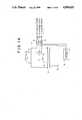
- a preferred embodiment of the invention for the epitaxial growth of Al x Ga 1-x As single crystal thin filmwill now be described with reference to the schematic view in FIG. 1.
- a substrate crystal 7 of GaAsis mounted on a quartz susceptor 8 disposed in a crystal growth vessel 11.
- the vessel 11is coupled to an evacuating system 13 via a gate valve 12 for evacuating its interior to an ultrahigh vacuum.
- the vessel 11is also provided with an infrared ray lamp 10 enclosed in a casing 9 for irradiating the GaAs substrate crystal 7.
- the vessel 11is further provided with three nozzle means 1, 2 and 3 for introducing alkyl aluminum as a gaseous compound containing aluminum (Al), alkyl gallium as a gaseous compound containing gallium (Ga) and arsine (AsH 3 ) as a gaseous compound containing arsenic (As), respectively.
- the nozzle means 1, 2 and 3are connected via respective controlling units (CTL's) 4, 5 and 6 for controlling the introduced amount (per unit time) of respective gaseous compounds to their external sources, respectively.
- the controlling units 4, 5 and 6are coupled to a controlling system 14 for controlling the introduction mode of the various gaseous compounds.
- a single Crystal thin film of Al x Ga 1-x Asis grown in a manner as described below.
- the vessel 11is evacuated to get a vacuum of about 10 -9 to 10 -10 Torr by opening the gate valve 12 and operating the evacuating system 13.
- the evacuating system 13may be constituted with a vacuum pump system comprising a combination of pump units such as cryopumps and molecular turbo pumps.
- the GaAs substrate 7is heated to a crystal growth temperature of 300° to 500° C. by the infrared ray lamp 10 and the growth temperature is kept constant.
- alkyl aluminum as a gaseous compound containing aluminum, alkyl gallium as a gaseous compound containing gallium and arsine )AsH 3 ) as a gaseous compound containing arsenicare introduced in the vessel II according to a manner that will be described, in more detail, below to carrying out the epitaxial growth of Al x Ga 1-x As single crystal while keeping the controllability of the thickness of Al x Ga 1-x As thin films within several angstroms.
- FIG. 1BExamples of the mode for introducing the three kinds of gaseous compounds will now be described with reference to FIG. 1B in which three examples of the mode are shown.
- on-off timings for the introduction of each gaseous compoundare controlled by the controlling system 14 while the introduced amount per unit time of each gaseous compound is controlled by the controlling units 4, 5 and 6, respectively.
- gaseous alkyl gallium as a gas containing Gais first introduced for a period of t 1 after an evacuation period of t 0 . Then, the vessel 11 is evacuated again by operating the gate valve 12. After a period of t 2 , gaseous alkyl aluminum is introduced as a gas containing Al for a period of t 3 . Then, the vessel 11 is evacuated again for a period of t 4 . Thereafter, gaseous arsine (AsH 3 ) is introduced as a gas containing As for a period of t 5 . As a result of this one cycle of the operation which requires a total period of t 6 , a single crystalline thin film which has a thickness of several angstroms is grown.
- AsH 3gaseous arsine
- t 00 to 5 sec
- t 11 to 6 sec
- t 20 to 5 sec
- t 31 to 6 sec
- t 40 to 5 sec
- t 55 to 20 sec
- t 67 to 47 sec.
- mode IIIn another mode shown in FIG. 1B as mode II, the same operation is carried out except that the order of the introduction between a gas containing Ga and a gas containing Al is interchanged.
- t 100 to 5 sec
- t 111 to 6 sec
- t 120 to 5 sec
- t 131 to 6 sec
- t 140 to 5 sec
- t 155 to 20 sec
- t 167 to 47 sec.
- a gas containing Asis introduced after the introduction and the evacuation period of a gas containing Al and, thereafter, the gas containing As is introduced again following the introduction and evacuation periods of a gas containing Ga.
- t 200 to 5 sec
- t 211 to 6 sec
- t 220 to 5 sec
- t 235 to 20 sec
- t 240 to 5 sec
- t 251 to 6 sec
- t 260 to 5 sec
- t 275 to 20 sec
- t 2812 to 72 sec.
- the internal pressure of the vessel 11is kept at 10 -6 to 10 -4 Torr during the introducing period of gaseous alkyl aluminum, 10 -6 to 10 -4 Torr during the introducing period of gaseous alkyl gallium and 10 -5 to 10 -3 Torr during the introducing period of gaseous arsine.
- TMAtrimethyl aluminum
- TEAtriethyl aluminum
- TIBAtriisobutyl aluminum
- TMAtrimethyl aluminum
- TAGtrimethyl gallium
- TAGtriethyl gallium
- AsH 3arsine
- the carrier density in an epitaxial layer of Al x Ga 1-x As which is formed by using TMA as alkyl aluminum and TMG as alkyl galliumis 10 18 to 10 20 cm -3 (p type) at room temperature.
- TEGis used as alkyl gallium
- the carrier density of 10 15 to 10 18 cm -3 (p-type)is obtained by the use of TEA as alkyl aluminum
- the carrier density of 10 13 to 10 15 cm -3 (p-type)is obtained by the use of TIBA as alkyl aluminum so that an Al x Ga 1-x As layer of higher purity may be obtained.
- an epitaxial Al x Ga 1-x As layer having the lowest carrier densitymay be obtained by the mode II.
- TEGalkyl gallium
- TIBAalkyl aluminum and AsH 3
- an epitaxial layer having the carrier density of 10 13 to 10 15 cm -3 (p-type)is grown in the mode II while a layer having the carrier density of 10 15 to 10 16 cm -3 (p-type) is grown in the mode I.
- the thickness of a thin film of Al x Ga 1-x As which is grown in a single cycle of the introduction of gasesis about 1 to 10 ⁇ .
- an epitaxial growth of Al x Ga 1-x As thin film having the thickness corresponding to a single monolayermay easily be obtained in the single cycle of the introduction of gases.
- the thickness of one single monolayeris about 2.8 ⁇ at (100) plane and about 3.3 ⁇ at (111) plane.
- any value within 0 to 1 for x the composition of Al in Al x Ga 1-x Asmay also be obtained by suitably selecting the internal pressure of the vessel 11 during the introducing period of each compound gas and the introducing period thereof.
- the temperature of the crystal growthis kept at a value of 300° to 500° C. Since the redistribution of the impurity profile is suppressed due to such a rather lower growth temperature and, in addition, since the controllability for the thickness of the thin film being grown is excellent, a steep impurity profile may be attained in a multilayer thin film comprising GaAs and Al x Ga 1-x As.
- FIG. 2shows a depthwise profile of the composition x in Al x Ga 1-x As included in a multilayer structure GaAs/Al x Ga 1-x As/GaAs/Al x Ga 1-x As . . . which is manufactured by using a group of materials (TEG-AsH 3 ) and another group of materials (TEG-TEA-AsH 3 ).
- the composition xis measured by the Auger electron spectroscopy.
- the thickness of a GaAs layer in this multilayer structureis attained in a similar manner to such as described above by using the group of materials (TEG-AsH 3 ) and repeating 100 cycles of the serial introduction of such compound gases.
- the thickness of an Al x Ga 1-x As in this multilayer structureis attained by using the group of materials (TEG-TEA-AsH 3 ) and repeating 250 cycles of the serial introduction of such compound gases. Conditions for such introduction of gases are set so as to obtain an x value of 0.36 to 0.37. As will be seen from the graph shown in FIG. 2, a hetero junction between GaAs and Al x Ga 1-x As which has a steep impurity profile may be obtained.
- FIG. 3Ashows a sectional view of a MIS (metal-insulator-semicondctor) capacitor manufactured as a trial by using a group of materials (TEG-TIBA-AsH 3 ).
- a layer 16 of Al x Ga 1-x Asis epitaxially grown at a temperature of 350° to 550° C. on a Si doped (3 ⁇ 10 6 cm -3 ) n-type GaAs substrate crystal 15.
- an electrode 18 of Alis formed and a terminal 19 is attached thereto.
- an electrode 17 of AuGeis formed and a terminal 20 is attached thereto.
- the thickness of the Al x Ga 1-x As layer 16is about 700 ⁇ and the diameter of the Al electrode 18 is 500 ⁇ m.
- C-Vcapacitance to voltage
- FIG. 3BThe capacitance to voltage (C-V) characteristic curve of the MIS capacitor is shown in FIG. 3B. It will be seen that a high purity epitaxial layer of Al x Ga 1-x As may be obtained. It will also be noted that, according to the present invention, crystals of good quality may be grown at a lower growth temperature in comparison with prior methods such as MO-CVD or MBE.
- FIG. 4Ashows a schematic view of a device for manufacturing Al x Ga 1-x As epitaxial layers of p-type and n-type by means of doping.
- One of gaseous compounds containing IV or VI group elementssuch as disilane (Si 2 H 6 ), selenium hydride (H 2 Se), dimethyl selenium (DMSe) and diethyl tellurium (DETe) is introduced from an external source thereof via a controlling unit 33 for controlling the introduced amount of the gaseous compound and a nozzle 31 into a crystal growth vessel 11.
- a controlling unit 33for controlling the introduced amount of the gaseous compound and a nozzle 31 into a crystal growth vessel 11.
- one of gaseous compoundssuch as dimethyl zinc (DMZn) and dimethyl cadmium (DMCd) is introduced from an external source thereof via a controlling unit 34 for controlling the introduced amount of the gaseous compound and a nozzle 32 into the vessel 11.
- the introduction timing of gases introduced through the nozzles 31 and 32is controlled by a controlling system 14 in a similar manner to that described with reference to FIG. 1A.
- Other parts and functions thereofare same as or correspond to that of FIG. 1A and the description will not be repeated here.
- An epitaxial layer of Si doped n-type Al x Ga 1-x Asmay, for example, be formed by introducing Si 2 H 6 and that of Zn doped p-type Al x Ga 1-x As may be formed by introducing DMZn
- the gas introduction modes for these casesare shown in FIG. 4B. These modes for the above described cases in which TEG as a gaseous compound containing Ga and TIBA as a gaseous compound containing Al are used by way of example will now be described.
- a mode IV of FIG. 4Bwhich is the case that Si 2 H 6 is introduced, various gaseous compounds are introduced in the order of TIBA, TEG, Si 2 H 6 and AsH 3 .
- any gaseous compound containing any III group element and a gaseous compound containing an impurity element which will occupy the sites of III group atoms in a crystalare alternately introduced.
- Such modeis most effective in the doping with the use of Si 2 H 6 and an n-type Al x Ga 1-x As (10 16 to 10 19 cm -3 ) layer may be manufactured.
- Another mode V in FIG. 4Bis the case in which DMZn is introduced.
- the most effective dopingis attained when various gases are introduced in the order of DMZn, TIBA, TEG and AsH3 as shown in the mode V and a p-type Al x Ga 1-x As (10 16 to 10 20 cm -3 ) layer may be manufactured.
- a gaseous compound containing an impuritymay be introduced before and after each introduction, in the order, of a gaseous compound containing III A group element, that containing III B group element and that containing V group element or, in the order, of V, III A and III B .
- main impuritiesare II, IV and VI group elements. These impurities may be introduced in the order, II, III a , III B , IV, V and VI.
- FIG. 5shows a further form of the crystal growth device, which is designed to irradiate the substrate crystal during the crystal growth.
- the substrate 7is irradiated with ultraviolet rays 23 and 24 which are emitted from external sources such as excimer lasers, argon ion lasers, xenon lamps or mercury lamps and transmitted through synthetic quartz windows 21 and 22.
- the crystal growth temperaturemay be reduced to ensure growth of a single crystal having a still higher quality.
- a high purity Al x Ga 1-x As epitaxial layer having a carrier density of about 10 14 cm -3may be obtained at a low growth temperature of 300° to 400° C. by using a group of materials (TEG-TIBA-AsH 3 )
- the doping efficiencymay be controlled by synchronizing an irradiation of light having a specific wave length with the doping periods such as the introduction periods of Si 2 H 6 or DMZn.
- two kinds of light 23 and 24 having different wave lengthsmay be available through the windows 21 and 22, respectively, to irradiate the substrate 7.
- FIG. 6shows a further embodiment of the crystal growth device for manufacturing quaternary alloys of III-V compound mixed crystals.
- gaseous alkyl indiumis introduced from an external source via a controlling unit (CTL) 44 for controlling the introduced amount of gaseous alkyl indium and a nozzle 41 into a crystal growth vessel 11.
- CTLcontrolling unit
- gaseous alkyl gallium via a controlling unit (CTL) 45 and a nozzle 42, and gaseous AsH 3 via a controlling unit (CTL) 46 and a nozzle 43are introduced, respectively, into the vessel 11.
- gaseous phosphine (PH 3 ) as an impurity gasis introduced from an external source thereof via a controlling unit 48 and a nozzle 47 into the vessel 11.
- an In x Ga 1-x As y P 1-y single crystalline thin filmmay be grown at a low temperature of 300° to 500° C. while keeping the controllability of the growing film thickness within several angstroms.
- a single crystalline thin film of Zn x Se 1-x Temay also be grown at a low temperature of 300° to 500° C. in a similar manner as described above by substituting dimethyl zinc (DMZn), selenium hydride (H 2 Se) and dimethyl tellurium (DMTe) for alkyl indium, alkyl gallium and AsH 3
- DMZndimethyl zinc
- H 2 Seselenium hydride
- DMTedimethyl tellurium
- a single crystalline thin film of Hg x Cd 1-x Temay also be grown by using gases of dimethyl mercury (DMHg), dimethyl cadmium (DMCd) and dimethyl tellurium (DMTe).
- DHgdimethyl mercury
- DMCddimethyl cadmium
- DMTedimethyl tellurium
- FIG. 7Ais an embodiment according to the present invention in which a manufacturing process for a superlattice structure is schematically shown.
- a GaAs layer 70 having the thickness d 1 and an Al x Ga 1-x As layer having the thickness d 2are alternately and successively grown.
- the thickness d 1 and d 2may be controlled dimensionally as precise as a monolayer.
- the minimum thickness in the superlattice structureis that of a monolayer.
- the thickness d 1 and d 2may easily be controlled so as to an arbitrary number of times of a single monolayer thickness may be attained as required.
- superlattice structuressuch as an n-GaAs/n-Al x Ga 1-x As superlattice structure and an n-GaAs/p-Al x Ga 1-x As superlattice structure may also be manufactured.
- FIG. 7Bshows the band structure of the n-GaAs/n-Al x Ga 1-x As superlattice structure comprising a band structure 72 of n-GaAs and a band structure 73 of n-Al x Ga 1-x As.
- FIG. 7Cshows the band structure of the n-GaAs/p-Al x Ga 1-x As superlattice structure comprising a band structure 72 of n-GaAs and a band structure 75 of p-Al x Ga 1-x As.
- each growth layermay be controlled in accordance with a predetermined design in like manner as the embodiment of FIG. 7A. Further, the doping may be carried out in the same manner such as shown in FIGS. 4A and 4B for Al x Ga 1-x As, and in like manner of FIG. 4B without Al for GaAs.
- an n-Al x Ga 1-x As/p-Al x Ga 1-x As superlattice structuremay also be manufactured according to the method shown in FIGS. 4A and 4B. Alternate doping of n-type and p-type impurities with or without changing the composition of Al in monolayer by monolayer manner may also be carried out. Of course, the thickness of n-Al x Ga 1-x As and p-Al x Ga 1-x As may be changed, respectively.
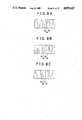
- FIGS. 8A to 8CEmbodiments of poly-type superlattice structures are shown in FIGS. 8A to 8C.
- FIGS. 8A to 8CThere are shown, by way of example, three those superlattice structures each comprising a combination of three kind of semiconductors such as, for example, InAs 80, AlSb 81 and GaSb 82.
- FIG. 8Ashows a superlattice structure comprising a unit periodic structure 80, 81 and 82
- FIG. 8Bshows a superlattice structure comprising a unit periodic structure 80, 81, 80 and 82
- FIG. 8Cshows a superlattice structure comprising a unit periodic structure 80, 82, 81 and 82.
- the combinations, conduction types of layers, the impurity density in each layer and the thickness of layersmay be changed as required.
- the superlattice structureis grown in monolayer by monolayer manner according to the method of the invention, ununiformity of microscopic atom configuration is eliminated from the manufactured mixed crystals so that the superlattice structure having a periodic structure produced by a combination of ideal mixed crystals regularly arranged in atomic accuracy may be manufactured. Furthermore, since the crystal growth may be carried out at a low temperature of about 300° C., a superlattice structure having a steep impurity profile may also be manufactured with the use of impurity doping.
- Undoped GaAs layer 91 having a thickness of about 200 monolayersis, first, grown on a semi-insulating GaAs substrate 90. Then, a Si doped Al x Ga 1-x As (x ⁇ 0.3) layer 93 having a thickness of 30 to 40 monolayers is grown. Thereafter, source, gate and drain electrodes are formed.
- the source electrode 94is an ohmic electrode of AuGe/Au and the gate electrode 95 is a Ti/Pt/Au electrode.
- the scatteringwhich may be occurred at the interface between the n-Al x Ga 1-x As layer 93 and the undoped GaAs layer 91, of electrons in a two-dimensional electron gas layer 92 is minimized so that a highly efficient transistor may be manufactured.
- any designed values of thickness of layers, composition x and impurity densitiesmay be attained.
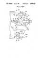
- FIG. 10Another process of the invention for manufacturing a diode utilizing the resonance tunneling effect will now be described with reference to FIG. 10 in which a schematic sectional view of such diode is shown.
- An n + -GaAs layer 101 having 100 monolayer thickness and an impurity density of about 10 8 cm -3is, first, grown on an n + -GaAs substrate 100.
- an Al x Ga 1-x As high resistance layer 102 having 15 to 20 monolayer thickness, an n-GaAs layer 103 having 15 to 20 monolayer thickness and an impurity density of 10 17 cm -3 , an Al x Ga 1-x As high resistance layer 104 having 15 to 20 monolayer thickness and an n + -GaAs layer 105 having 100 monolayer thickness and an impurity density of cm -3are successively grown.
- an ohmic contact 106 of such as, for example, AuGe/Niis formed on the top surface of the layer 105 and the bottom surface of the substrate 100, respectively.
- Such a devicewill exhibit a negative resistance when a DC voltage is applied in normal or reversed direction at 4K to the room temperature so that the device is available as an oscillator, a mixer or a detector in millimeter wave and submillimeter wave bands.
- FIG. 11Still another process of the invention for manufacturing a transistor in which the resonant tunneling structure such as described above is disposed in the channel of a field effect transistor will now be described with reference to FIG. 11 in which a schematic sectional view of such transistor is shown.
- the impurity densitymay be designed to have a value less than about 10 16 cm -3 so that the velocity of electrons may not be affected due to the lattice scattering in these regions.
- a source electrode 112 and a drain electrode 113are formed by Au-Ge/Ni/Au while a gate electrode 114 is formed with a Schottky gate of such as Al, Pt, Mo and Cr or an ohmic electrode of such as well known Au-Ge/Ni/Au.
- the thickness of the drain regionmay be designed so as to result the transit angle ⁇ of 3 ⁇ /2 if the time constant between gate and source is negligible and the maximum injection at a phase of ⁇ /4 is intended while that of the drain region may be designed so as to result the transit angle of ⁇ /2 to ⁇ if the time constant between gate and source is no longer negligible and the maximum injection at a phase of ⁇ /2 to ⁇ is intended.
- f osc maxV s /2W where V s and W are the carrier velocity and the thickness of the drain region, respectively.
- the thickness of the resonance tunneling parts 102 to 104is reduced corresponding to the increasing f c 's
- the impurity density in n + -GaAs layers 101 and 105may be designed as more than 10 18 cm -3 while that in the resonance tunneling junction may be designed as same as that in FIG. 10 or a predetermined value.
- the crystal growth method of the inventionmay equally well be embodied for manufacturing ultra thin film structures other than the embodiments such as described above with reference to FIGS. 7 to 11. Also, the embodiments has been described above referring to GaAs and Al x Ga 1-x As as growth layers. The process of the invention, however, may also be applied to such as other III-V compounds and mixed crystals thereof, II-VI compounds and mixed crystals thereof, and hetero-junctions between III-V and II-VI compounds.
- FIGS. 12Ais a schematic block diagram of an epitaxial growth device including controlling parts thereof for carrying out the process according to the invention.
- the devicecomprises a crystal growth vessel 150, a gate valve 151, an evacuating system 152, a driving means 153 for driving the gate valve 151, a vacuum gauge 154, a quartz susceptor 155 for mounting a semiconductor substrate 156, a lamp 158 for heating the semiconductor substrate 156 and a lamp housing 157. Most of these parts correspond to those parts shown in FIGS. 1A, 4A, 5 and 6.
- the heating temperature of the lamp 158is controlled by a lamp temperature controlling unit 159 comprising such a power supply and a thermostat.
- the temperature of the substrate 156is observed by a radiation thermometer or pyrometer 161 through a window 160.
- An output 162 from the thermometeris transmitted with an output 163 for monitoring the lamp heating temperature to a temperature controlling unit 165 for controlling the temperature of the substrate from which a signal 164 is transmitted to the unit 159.
- the internal pressure of the vessel 150is measured by the vacuum gauge 154 and an output signal 168 of the vacuum gauge 154 is transmitted to a controlling unit 166 for controlling the evacuating system 152.
- a controlling signal 167 from the unit 166is transmitted to the evacuating system 152 and the driving means 153.
- Gaseous compounds 170, 171, 172, 173 and 174 containing one of component elements or impurity elements, respectively,are introduced via respective stop valve 180, 181, 182, 183 and 184, respective controlling unit 190, 191, 192, 193 and 194, and respective nozzle 200, 201, 202, 203 and 204 into the vessel 150.
- Manually operated valves or electromagnetic valvesmay be available for the valves 180, 181, 182, 183 and 184.
- the controlling units 190, 191, 192, 193 and 194control the pressure and the introducing periods of each gaseous compound, respectively. The manner to control the pressure and the introduction periods of each gaseous compound will, hereinafter, be described more specifically with reference to FIG. 12B.
- Input signals to control the units 190, 191, 192, 193 and 194, respectively, and output monitoring signals thereofare transmitted via signal lines 210, 211, 212, 213 and 214, respectively.
- a controlling systemcomprising a computer CPU 220, an input terminal 221, a memory 222, an image output terminal 23 and an output printer operating system not shown is connected through an interface circuit 215 to the group of units 190, 191, 192, 193 and 194.
- the computertransmits a controlling signal 232.
- the computertransmits a controlling signal 230.
- FIG. 12Bshows a schematic block diagram illustrating a part of the gas controlling unit. Since the manner of the operation of various units 190 to 194 is the same, the description will be limited only to the introduction of one gaseous compound. Thus, the operation, for example, of the unit 190 will be described.
- the introduction of the gaseous compound 170is controlled by a stop valve 251 controlling introducing and non-introducing periods in response to a control signal transmitted from the computer through the line 210.
- the pressure of the gaseous compound 170is controlled by a mass flow controller 252 in response to an output controlling signal 257 from a pressure controlling circuit 255.
- the pressure controlling circuit 255is an electronic circuit comprising a feedback control using such as well known transistors, diodes and IC's.
- the circuit 255generates the output controlling signal 257 in response to an output signal 254 from a manometer 253 and a controlling signal 256 generated from the computer in response to the output signal 254 of the manometer 253.
- FIG. 12Cthere is shown a mode for the introduction of various gases together with a temperature controlling diagram which may be used for carrying out a crystal growth process in which n-GaAs layers and p-Al x Ga 1-x As layers are alternately grown on an n-GaAs substrate in monolayer by monolayer manner by means of the controlling system described above.
- a single monolayer of n-GaAsmay be grown at a temperature T 50 and, subsequently, a single monolayer of p-Al x Ga 1-x As may be grown in a period of t 51 temperature T 51 .
- an epitaxial layer of such as 100 or 1000 monolayer thicknessmay also be grown.
- a program, in an appropriate language, instructing 100 or 1000 monolayer thicknessmay be input to the computer.
- any desired ultrathin film structuremay be grown. Since a crystal growth of a layer, for example, of two monolayer thickness may be carried out by adjusting the condition, such manner may be available for the save of growth time.
- a visual monitoringmay be carried out.
- memory devicessuch as a floppy disk, a cassette tape recorder and a hard disk may be used as the memory 222 for recording and reproducing the program of the process for manufacturing the ultrathin film structure.
- consecutive crystal growthmay be carried out by using an automatic transport device for the insertion and take out operations of the substrate into and out of the crystal growth vessel.
- the mass production of an ultrathin film comprising layers of different structuresmay be carried out by using a controlling program such as described above in combination with a program for controlling the automatic transport device.
- the monolayer growthmay be carried out in a simple manner by using a simple manometer and a controlling system for controlling the gas introduction and the substrate temperature, high quality wafers comprising ultrathin epitaxial layers may easily be manufactured in contrast to the MBE method.
- FIG. 12Athere is shown only one input terminal.
- an operating system of multitask or multijob typecomprising a plurality of input terminals to the computer may also be used for carrying out the crystal growth control while programming other new programs for the crystal growth.
- Still another embodiment of the inventionin which the irradiation of the substrate with light during the crystal growth such as shown in FIG. 5 is automated, will now be described.
- Ultraviolet rays 280 and 281 emitted from ultraviolet ray sources 273 and 276 such as mercury lamps, excimer lasers and argon ion lasers, respectively,are introduced via shutters 271 and 275, and windows 270 and 274, respectively, to a substrate 156.
- the shutters 271 and 275are operated by controlling signals 293 and 294 through an interface circuit 292.
- FIG. 13BA manner of the irradiation with light 1 and light 2 which is accompanied with the crystal growth process shown in FIG. 12C is shown in FIG. 13B.
- the irradiation with light 1is continued before the introduction of compound gas containing As is started and the irradiation with light 2 follows.
- the irradiation with light 2is continued before the introduction of DMZn gas.
- Wave lengths of light 1 and light 2may be selected so as to activate the surface reaction during the irradiation. Such a case may also be possible that light 1 and light 2 have the same wave length but different intensities. Also, light having a range of wave lengths may be used for light 280 and 281, respectively.
- two or more kinds of light having different wave lengthsmay be substituted for light 280 and 281, respectively, so as to irradiate the substrate with different kinds of light corresponding to the introduction or non-introduction periods of different kind of gases thereby more effective crystal growth may be carried out.
- the irradiation of semiconductor substrate with one light source but two kinds of light having two different range of wave lengthsmay be carried out by using a shutter with a filter.
- III-V mixed crystalshave been referred to by way of example, the invention is of course also applicable to II-VI mixed crystal, compound semiconductors containing four elements or heter-junctions between III-V mixed crystals and II-VI mixed crystals merely by additionally installing more gas introduction units to the embodiments shown in FIGS. 12 and 13 as desired.
- the crystal growth of mixed crystals having ultrathin film structure with impurity dopingwhich has been difficult in the prior art, may be carried out in monolayer accuracy.
- the prior artsuch as the MBE method
- the process of the inventionsuch as described above may be automated in a simple manner by an inexpensive controlling device for controlling the pressure of gases, the introduction of gases, the temperature of the substrate and the irradiation with light.
- the crystal growth method of the inventionis suitable for the mass production of ultrathin film structures in high accuracy and effective in the industrial utilization.
- various devicessuch as hetero-junction devices, HEMT structure devices, superlattice structure devices, two or three terminal devices, negative resistance devices utilizing the transit time effect, tunnel injection devices, optical detector or light emitting devices, and semiconductor lasers may be manufactured.
Landscapes
- Engineering & Computer Science (AREA)
- Chemical & Material Sciences (AREA)
- Manufacturing & Machinery (AREA)
- General Physics & Mathematics (AREA)
- Physics & Mathematics (AREA)
- Computer Hardware Design (AREA)
- Microelectronics & Electronic Packaging (AREA)
- Power Engineering (AREA)
- Condensed Matter Physics & Semiconductors (AREA)
- Materials Engineering (AREA)
- Crystallography & Structural Chemistry (AREA)
- Metallurgy (AREA)
- Organic Chemistry (AREA)
- Inorganic Chemistry (AREA)
- Chemical Kinetics & Catalysis (AREA)
- General Chemical & Material Sciences (AREA)
- Junction Field-Effect Transistors (AREA)
- Crystals, And After-Treatments Of Crystals (AREA)
Abstract
Description
Claims (22)
Applications Claiming Priority (2)
| Application Number | Priority Date | Filing Date | Title |
|---|---|---|---|
| JP61-277829 | 1986-11-22 | ||
| JP61277829AJP2587623B2 (en) | 1986-11-22 | 1986-11-22 | Epitaxial crystal growth method for compound semiconductor |
Publications (1)
| Publication Number | Publication Date |
|---|---|
| US4859625Atrue US4859625A (en) | 1989-08-22 |
Family
ID=17588846
Family Applications (1)
| Application Number | Title | Priority Date | Filing Date |
|---|---|---|---|
| US07/123,497Expired - LifetimeUS4859625A (en) | 1986-11-22 | 1987-11-20 | Method for epitaxial growth of compound semiconductor using MOCVD with molecular layer epitaxy |
Country Status (5)
| Country | Link |
|---|---|
| US (1) | US4859625A (en) |
| JP (1) | JP2587623B2 (en) |
| DE (1) | DE3739639A1 (en) |
| FR (1) | FR2607322B1 (en) |
| GB (1) | GB2198454B (en) |
Cited By (47)
| Publication number | Priority date | Publication date | Assignee | Title |
|---|---|---|---|---|
| US5123995A (en)* | 1990-10-04 | 1992-06-23 | Aerodyne Research, Inc. | Low-temperature, photo-induced epitaxy |
| US5204284A (en)* | 1989-01-19 | 1993-04-20 | Hewlett-Packard Company | Method of making a high band-gap opto-electronic device |
| US5213654A (en)* | 1990-05-18 | 1993-05-25 | Kabushiki Kaisha Toshiba | Vapor-phase epitaxial growth method for semiconductor crystal layers |
| US5225366A (en)* | 1990-06-22 | 1993-07-06 | The United States Of America As Represented By The Secretary Of The Navy | Apparatus for and a method of growing thin films of elemental semiconductors |
| US5229319A (en)* | 1989-11-30 | 1993-07-20 | Kabushiki Kaisha Toshiba | Method for producing compound semiconductors and apparatus therefor |
| US5270247A (en)* | 1991-07-12 | 1993-12-14 | Fujitsu Limited | Atomic layer epitaxy of compound semiconductor |
| US5322808A (en)* | 1991-08-21 | 1994-06-21 | Hughes Aircraft Company | Method of fabricating inverted modulation-doped heterostructure |
| US5755886A (en)* | 1986-12-19 | 1998-05-26 | Applied Materials, Inc. | Apparatus for preventing deposition gases from contacting a selected region of a substrate during deposition processing |
| US5997589A (en)* | 1998-07-09 | 1999-12-07 | Winbond Electronics Corp. | Adjustment pumping plate design for the chamber of semiconductor equipment |
| US6010937A (en)* | 1995-09-05 | 2000-01-04 | Spire Corporation | Reduction of dislocations in a heteroepitaxial semiconductor structure |
| US6316098B1 (en) | 1998-03-27 | 2001-11-13 | Yissum Research Development Company Of The Hebrew University Of Jerusalem | Molecular layer epitaxy method and compositions |
| US6334901B1 (en)* | 1984-07-26 | 2002-01-01 | Japan Science And Technology Corporation | Apparatus for forming semiconductor crystal |
| US20020083897A1 (en)* | 2000-12-29 | 2002-07-04 | Applied Materials, Inc. | Full glass substrate deposition in plasma enhanced chemical vapor deposition |
| US6551929B1 (en) | 2000-06-28 | 2003-04-22 | Applied Materials, Inc. | Bifurcated deposition process for depositing refractory metal layers employing atomic layer deposition and chemical vapor deposition techniques |
| KR100384558B1 (en)* | 2001-02-22 | 2003-05-22 | 삼성전자주식회사 | Method for forming dielectric layer and capacitor using thereof |
| US20030132213A1 (en)* | 2000-12-29 | 2003-07-17 | Kim Sam H. | Apparatus and method for uniform substrate heating and contaminate collection |
| US6620723B1 (en) | 2000-06-27 | 2003-09-16 | Applied Materials, Inc. | Formation of boride barrier layers using chemisorption techniques |
| US6620670B2 (en) | 2002-01-18 | 2003-09-16 | Applied Materials, Inc. | Process conditions and precursors for atomic layer deposition (ALD) of AL2O3 |
| US20030189232A1 (en)* | 2002-04-09 | 2003-10-09 | Applied Materials, Inc. | Deposition of passivation layers for active matrix liquid crystal display (AMLCD) applications |
| US20030194825A1 (en)* | 2002-04-10 | 2003-10-16 | Kam Law | Deposition of gate metallization for active matrix liquid crystal display (AMLCD) applications |
| US6660126B2 (en) | 2001-03-02 | 2003-12-09 | Applied Materials, Inc. | Lid assembly for a processing system to facilitate sequential deposition techniques |
| US6720027B2 (en) | 2002-04-08 | 2004-04-13 | Applied Materials, Inc. | Cyclical deposition of a variable content titanium silicon nitride layer |
| US6729824B2 (en) | 2001-12-14 | 2004-05-04 | Applied Materials, Inc. | Dual robot processing system |
| US6734020B2 (en) | 2001-03-07 | 2004-05-11 | Applied Materials, Inc. | Valve control system for atomic layer deposition chamber |
| US20040142558A1 (en)* | 2002-12-05 | 2004-07-22 | Granneman Ernst H. A. | Apparatus and method for atomic layer deposition on substrates |
| US6783849B2 (en) | 1998-03-27 | 2004-08-31 | Yissum Research Development Company Of The Hebrew University Of Jerusalem | Molecular layer epitaxy method and compositions |
| US6827978B2 (en) | 2002-02-11 | 2004-12-07 | Applied Materials, Inc. | Deposition of tungsten films |
| US20040255861A1 (en)* | 2000-12-29 | 2004-12-23 | Quanyuan Shang | Chamber for uniform substrate heating |
| US20050000937A1 (en)* | 2000-12-06 | 2005-01-06 | Chiang Tony P. | Temperature control system in an ALD chamber |
| US6846516B2 (en) | 2002-04-08 | 2005-01-25 | Applied Materials, Inc. | Multiple precursor cyclical deposition system |
| US6875271B2 (en) | 2002-04-09 | 2005-04-05 | Applied Materials, Inc. | Simultaneous cyclical deposition in different processing regions |
| US6878206B2 (en) | 2001-07-16 | 2005-04-12 | Applied Materials, Inc. | Lid assembly for a processing system to facilitate sequential deposition techniques |
| US6911391B2 (en) | 2002-01-26 | 2005-06-28 | Applied Materials, Inc. | Integration of titanium and titanium nitride layers |
| US6916398B2 (en) | 2001-10-26 | 2005-07-12 | Applied Materials, Inc. | Gas delivery apparatus and method for atomic layer deposition |
| US20050164487A1 (en)* | 2001-02-02 | 2005-07-28 | Applied Materials, Inc. | Formation of a tantalum-nitride layer |
| US6936906B2 (en) | 2001-09-26 | 2005-08-30 | Applied Materials, Inc. | Integration of barrier layer and seed layer |
| US6998579B2 (en) | 2000-12-29 | 2006-02-14 | Applied Materials, Inc. | Chamber for uniform substrate heating |
| US7049226B2 (en) | 2001-09-26 | 2006-05-23 | Applied Materials, Inc. | Integration of ALD tantalum nitride for copper metallization |
| US20060172534A1 (en)* | 2002-11-12 | 2006-08-03 | Doan Trung T | Atomic layer deposition methods |
| US7101795B1 (en) | 2000-06-28 | 2006-09-05 | Applied Materials, Inc. | Method and apparatus for depositing refractory metal layers employing sequential deposition techniques to form a nucleation layer |
| US7115499B2 (en)* | 2002-02-26 | 2006-10-03 | Applied Materials, Inc. | Cyclical deposition of tungsten nitride for metal oxide gate electrode |
| US20060229528A1 (en)* | 2003-03-29 | 2006-10-12 | C. R. Brad, Inc. | Coaxial cannula provided with a sealing element |
| US7405158B2 (en) | 2000-06-28 | 2008-07-29 | Applied Materials, Inc. | Methods for depositing tungsten layers employing atomic layer deposition techniques |
| US7439191B2 (en) | 2002-04-05 | 2008-10-21 | Applied Materials, Inc. | Deposition of silicon layers for active matrix liquid crystal display (AMLCD) applications |
| US7732327B2 (en) | 2000-06-28 | 2010-06-08 | Applied Materials, Inc. | Vapor deposition of tungsten materials |
| US7964505B2 (en) | 2005-01-19 | 2011-06-21 | Applied Materials, Inc. | Atomic layer deposition of tungsten materials |
| US20150225846A1 (en)* | 2012-07-27 | 2015-08-13 | Tokyo Electron Limited | ZnO FILM PRODUCTION DEVICE, AND PRODUCTION METHOD |
Families Citing this family (7)
| Publication number | Priority date | Publication date | Assignee | Title |
|---|---|---|---|---|
| JPH02260417A (en)* | 1989-03-30 | 1990-10-23 | Mitsubishi Electric Corp | Crystal growth method and device for semiconductor thin film |
| JPH06295862A (en)* | 1992-11-20 | 1994-10-21 | Mitsubishi Electric Corp | Compound semiconductor fabrication system and organic metal material vessel |
| DE10049257B4 (en)* | 1999-10-06 | 2015-05-13 | Samsung Electronics Co., Ltd. | Process for thin film production by means of atomic layer deposition |
| US6576053B1 (en) | 1999-10-06 | 2003-06-10 | Samsung Electronics Co., Ltd. | Method of forming thin film using atomic layer deposition method |
| JP4972995B2 (en)* | 2006-05-17 | 2012-07-11 | 富士通株式会社 | Quantum dot semiconductor device |
| JP2008306176A (en)* | 2007-05-08 | 2008-12-18 | Tokyo Electron Ltd | Method and apparatus for heat treatment of compound semiconductor |
| JP5668602B2 (en)* | 2011-05-30 | 2015-02-12 | 日立金属株式会社 | Method and apparatus for growing semi-insulating nitride semiconductor layer |
Citations (6)
| Publication number | Priority date | Publication date | Assignee | Title |
|---|---|---|---|---|
| US3626257A (en)* | 1969-04-01 | 1971-12-07 | Ibm | Semiconductor device with superlattice region |
| US3867202A (en)* | 1973-03-15 | 1975-02-18 | Sumitomo Chemical Co | Chemical vapor deposition for epitaxial growth |
| US3979235A (en)* | 1974-01-10 | 1976-09-07 | U.S. Philips Corporation | Depositing doped material on a substrate |
| US4058430A (en)* | 1974-11-29 | 1977-11-15 | Tuomo Suntola | Method for producing compound thin films |
| US4504331A (en)* | 1983-12-08 | 1985-03-12 | International Business Machines Corporation | Silicon dopant source in intermetallic semiconductor growth operations |
| GB2162206A (en)* | 1984-07-26 | 1986-01-29 | Japan Res Dev Corp | Process for forming monocrystalline thin film of element semiconductor |
Family Cites Families (6)
| Publication number | Priority date | Publication date | Assignee | Title |
|---|---|---|---|---|
| US3721583A (en)* | 1970-12-08 | 1973-03-20 | Ibm | Vapor phase epitaxial deposition process for forming superlattice structure |
| FI57975C (en)* | 1979-02-28 | 1980-11-10 | Lohja Ab Oy | OVER ANCHORING VIDEO UPDATE FOR AVAILABILITY |
| JPH0766910B2 (en)* | 1984-07-26 | 1995-07-19 | 新技術事業団 | Semiconductor single crystal growth equipment |
| JPH0782991B2 (en)* | 1984-07-26 | 1995-09-06 | 新技術事業団 | Method of growing compound semiconductor single crystal thin film |
| GB2162862B (en)* | 1984-07-26 | 1988-10-19 | Japan Res Dev Corp | A method of growing a thin film single crystalline semiconductor |
| US4767494A (en)* | 1986-07-04 | 1988-08-30 | Nippon Telegraph & Telephone Corporation | Preparation process of compound semiconductor |
- 1986
- 1986-11-22JPJP61277829Apatent/JP2587623B2/ennot_activeExpired - Lifetime
- 1987
- 1987-11-20USUS07/123,497patent/US4859625A/ennot_activeExpired - Lifetime
- 1987-11-20GBGB8727278Apatent/GB2198454B/ennot_activeExpired
- 1987-11-23DEDE19873739639patent/DE3739639A1/enactiveGranted
- 1987-11-23FRFR878716212Apatent/FR2607322B1/ennot_activeExpired - Lifetime
Patent Citations (6)
| Publication number | Priority date | Publication date | Assignee | Title |
|---|---|---|---|---|
| US3626257A (en)* | 1969-04-01 | 1971-12-07 | Ibm | Semiconductor device with superlattice region |
| US3867202A (en)* | 1973-03-15 | 1975-02-18 | Sumitomo Chemical Co | Chemical vapor deposition for epitaxial growth |
| US3979235A (en)* | 1974-01-10 | 1976-09-07 | U.S. Philips Corporation | Depositing doped material on a substrate |
| US4058430A (en)* | 1974-11-29 | 1977-11-15 | Tuomo Suntola | Method for producing compound thin films |
| US4504331A (en)* | 1983-12-08 | 1985-03-12 | International Business Machines Corporation | Silicon dopant source in intermetallic semiconductor growth operations |
| GB2162206A (en)* | 1984-07-26 | 1986-01-29 | Japan Res Dev Corp | Process for forming monocrystalline thin film of element semiconductor |
Non-Patent Citations (24)
| Title |
|---|
| Aoyagi et al., "Atomic-Layer Growth of GaAs by Modulated . . .", J. Vac. Sci. Technol. B5(5), Sep./Oct. 1987, pp. 1460-1464. |
| Aoyagi et al., Atomic Layer Growth of GaAs by Modulated . . . , J. Vac. Sci. Technol. B5(5), Sep./Oct. 1987, pp. 1460 1464.* |
| Balk et al., "Ultraviolet Induced Metal-Organic Chemical Vapor Deposition Growth of GaAs", J. Vac. Sci. Technol. A4(3), May/Jun. 1986, pp. 711-715. |
| Balk et al., Ultraviolet Induced Metal Organic Chemical Vapor Deposition Growth of GaAs , J. Vac. Sci. Technol. A4(3), May/Jun. 1986, pp. 711 715.* |
| Bedair et al., Appl. Phys. Lett. 48(2), 13 Jan. 1986, pp. 174 176.* |
| Bedair et al., Appl. Phys. Lett. 48(2), 13 Jan. 1986, pp. 174-176. |
| Doi et al., "Growth of GaAs by Switched Laser Metalorganic Vapor Phase Epitaxy", Appl. Phys. Lett. 48(26), 30 Jun. 1986, pp. 1787-1789. |
| Doi et al., "Stepwise Monolayer Growth of GaAs by Switched Laser Metalorganic Vapor Phase Epitaxy", Appl. Phys. Lett. 49(13), 29 Sep. 1986, pp. 785-787. |
| Doi et al., Growth of GaAs by Switched Laser Metalorganic Vapor Phase Epitaxy , Appl. Phys. Lett. 48(26), 30 Jun. 1986, pp. 1787 1789.* |
| Doi et al., Stepwise Monolayer Growth of GaAs by Switched Laser Metalorganic Vapor Phase Epitaxy , Appl. Phys. Lett. 49(13), 29 Sep. 1986, pp. 785 787.* |
| Kobayashi et al., "Flow-Rate Modulation Epitaxy of GaAs", Inst. Phys. Conf. Ser. No. 79, Chapter 13, 1985, pp. 737-738. |
| Kobayashi et al., Flow Rate Modulation Epitaxy of GaAs , Inst. Phys. Conf. Ser. No. 79, Chapter 13, 1985, pp. 737 738.* |
| Nishizawa et al., "Molecular Layer Epitaxy", J. Electrochem. Soc. May 1985, pp. 1197-1200. |
| Nishizawa et al., "Photostimulated Molecular Layer Epitaxy", J. Vac. Sci. Technol. A4(3), May/Jun. 1986, pp. 706-710. |
| Nishizawa et al., Molecular Layer Epitaxy , J. Electrochem. Soc. May 1985, pp. 1197 1200.* |
| Nishizawa et al., Photostimulated Molecular Layer Epitaxy , J. Vac. Sci. Technol. A4(3), May/Jun. 1986, pp. 706 710.* |
| Pessa et al., "Atomic Layer Epitaxy . . . of cdte Films . . .", J. Appl. Phys. 54(10), Oct. 1983, pp. 6047-6050. |
| Pessa et al., Atomic Layer Epitaxy . . . of cdte Films . . . , J. Appl. Phys. 54(10), Oct. 1983, pp. 6047 6050.* |
| Razeghi et al., "Monolayer Epitaxy of III-V Compounds . . .", Appl. Phys. Lett. 51(26), 28 Dec. 1987, pp. 2216-2218. |
| Razeghi et al., Monolayer Epitaxy of III V Compounds . . . , Appl. Phys. Lett. 51(26), 28 Dec. 1987, pp. 2216 2218.* |
| Sakaki et al., "One Atomic Layer Heterointerface Fluctuations in GaAs--AlAs . . .", Jan. 5 Appl. Phys., vol. 24, No. 6, Jun. 1985, pp. L417-L420. |
| Sakaki et al., One Atomic Layer Heterointerface Fluctuations in GaAs AlAs . . . , Jan. 5 Appl. Phys., vol. 24, No. 6, Jun. 1985, pp. L417 L420.* |
| Usui et al., "GaAs Atomic Layer Epitaxy by Hydride VPE", Jpn. J. Appl. Phys., vol. 25, No. 3, Mar. 1986, pp. L212-L214. |
| Usui et al., GaAs Atomic Layer Epitaxy by Hydride VPE , Jpn. J. Appl. Phys., vol. 25, No. 3, Mar. 1986, pp. L212 L214.* |
Cited By (86)
| Publication number | Priority date | Publication date | Assignee | Title |
|---|---|---|---|---|
| US6334901B1 (en)* | 1984-07-26 | 2002-01-01 | Japan Science And Technology Corporation | Apparatus for forming semiconductor crystal |
| US5871811A (en)* | 1986-12-19 | 1999-02-16 | Applied Materials, Inc. | Method for protecting against deposition on a selected region of a substrate |
| US5755886A (en)* | 1986-12-19 | 1998-05-26 | Applied Materials, Inc. | Apparatus for preventing deposition gases from contacting a selected region of a substrate during deposition processing |
| US5204284A (en)* | 1989-01-19 | 1993-04-20 | Hewlett-Packard Company | Method of making a high band-gap opto-electronic device |
| US5229319A (en)* | 1989-11-30 | 1993-07-20 | Kabushiki Kaisha Toshiba | Method for producing compound semiconductors and apparatus therefor |
| US5213654A (en)* | 1990-05-18 | 1993-05-25 | Kabushiki Kaisha Toshiba | Vapor-phase epitaxial growth method for semiconductor crystal layers |
| US5225366A (en)* | 1990-06-22 | 1993-07-06 | The United States Of America As Represented By The Secretary Of The Navy | Apparatus for and a method of growing thin films of elemental semiconductors |
| US5123995A (en)* | 1990-10-04 | 1992-06-23 | Aerodyne Research, Inc. | Low-temperature, photo-induced epitaxy |
| US5270247A (en)* | 1991-07-12 | 1993-12-14 | Fujitsu Limited | Atomic layer epitaxy of compound semiconductor |
| US5322808A (en)* | 1991-08-21 | 1994-06-21 | Hughes Aircraft Company | Method of fabricating inverted modulation-doped heterostructure |
| US6010937A (en)* | 1995-09-05 | 2000-01-04 | Spire Corporation | Reduction of dislocations in a heteroepitaxial semiconductor structure |
| US6316098B1 (en) | 1998-03-27 | 2001-11-13 | Yissum Research Development Company Of The Hebrew University Of Jerusalem | Molecular layer epitaxy method and compositions |
| US6783849B2 (en) | 1998-03-27 | 2004-08-31 | Yissum Research Development Company Of The Hebrew University Of Jerusalem | Molecular layer epitaxy method and compositions |
| US6808803B1 (en) | 1998-03-27 | 2004-10-26 | Yissum Research Development Company Of The Hebrew University Of Jerusalem | Molecular epitaxy method and compositions |
| US20040202875A1 (en)* | 1998-03-27 | 2004-10-14 | Yissum Res & Dev Co Of Hebrew Univ Of Jerusalem | Molecular epitaxy method and compositions |
| US5997589A (en)* | 1998-07-09 | 1999-12-07 | Winbond Electronics Corp. | Adjustment pumping plate design for the chamber of semiconductor equipment |
| US7501344B2 (en) | 2000-06-27 | 2009-03-10 | Applied Materials, Inc. | Formation of boride barrier layers using chemisorption techniques |
| US6620723B1 (en) | 2000-06-27 | 2003-09-16 | Applied Materials, Inc. | Formation of boride barrier layers using chemisorption techniques |
| US6551929B1 (en) | 2000-06-28 | 2003-04-22 | Applied Materials, Inc. | Bifurcated deposition process for depositing refractory metal layers employing atomic layer deposition and chemical vapor deposition techniques |
| US7846840B2 (en) | 2000-06-28 | 2010-12-07 | Applied Materials, Inc. | Method for forming tungsten materials during vapor deposition processes |
| US7115494B2 (en) | 2000-06-28 | 2006-10-03 | Applied Materials, Inc. | Method and system for controlling the presence of fluorine in refractory metal layers |
| US7235486B2 (en) | 2000-06-28 | 2007-06-26 | Applied Materials, Inc. | Method for forming tungsten materials during vapor deposition processes |
| US7101795B1 (en) | 2000-06-28 | 2006-09-05 | Applied Materials, Inc. | Method and apparatus for depositing refractory metal layers employing sequential deposition techniques to form a nucleation layer |
| US7745333B2 (en) | 2000-06-28 | 2010-06-29 | Applied Materials, Inc. | Methods for depositing tungsten layers employing atomic layer deposition techniques |
| US7405158B2 (en) | 2000-06-28 | 2008-07-29 | Applied Materials, Inc. | Methods for depositing tungsten layers employing atomic layer deposition techniques |
| US7732327B2 (en) | 2000-06-28 | 2010-06-08 | Applied Materials, Inc. | Vapor deposition of tungsten materials |
| US7465666B2 (en) | 2000-06-28 | 2008-12-16 | Applied Materials, Inc. | Method for forming tungsten materials during vapor deposition processes |
| US7033922B2 (en) | 2000-06-28 | 2006-04-25 | Applied Materials. Inc. | Method and system for controlling the presence of fluorine in refractory metal layers |
| US7674715B2 (en) | 2000-06-28 | 2010-03-09 | Applied Materials, Inc. | Method for forming tungsten materials during vapor deposition processes |
| US7601393B2 (en) | 2000-12-06 | 2009-10-13 | Novellus Systems, Inc. | Controlling the temperature of a substrate in a film deposition apparatus |
| US20050011457A1 (en)* | 2000-12-06 | 2005-01-20 | Chiang Tony P. | Controlling the temperature of a substrate in a film deposition apparatus |
| US20070184189A1 (en)* | 2000-12-06 | 2007-08-09 | Novellus Systems, Inc. | Controlling the Temperature of a Substrate in a Film Deposition Apparatus |
| US20050000937A1 (en)* | 2000-12-06 | 2005-01-06 | Chiang Tony P. | Temperature control system in an ALD chamber |
| US20030132213A1 (en)* | 2000-12-29 | 2003-07-17 | Kim Sam H. | Apparatus and method for uniform substrate heating and contaminate collection |
| US6825447B2 (en) | 2000-12-29 | 2004-11-30 | Applied Materials, Inc. | Apparatus and method for uniform substrate heating and contaminate collection |
| US20040255861A1 (en)* | 2000-12-29 | 2004-12-23 | Quanyuan Shang | Chamber for uniform substrate heating |
| US20020083897A1 (en)* | 2000-12-29 | 2002-07-04 | Applied Materials, Inc. | Full glass substrate deposition in plasma enhanced chemical vapor deposition |
| US6998579B2 (en) | 2000-12-29 | 2006-02-14 | Applied Materials, Inc. | Chamber for uniform substrate heating |
| US7022948B2 (en) | 2000-12-29 | 2006-04-04 | Applied Materials, Inc. | Chamber for uniform substrate heating |
| US7094680B2 (en) | 2001-02-02 | 2006-08-22 | Applied Materials, Inc. | Formation of a tantalum-nitride layer |
| US7781326B2 (en) | 2001-02-02 | 2010-08-24 | Applied Materials, Inc. | Formation of a tantalum-nitride layer |
| US9012334B2 (en) | 2001-02-02 | 2015-04-21 | Applied Materials, Inc. | Formation of a tantalum-nitride layer |
| US8114789B2 (en) | 2001-02-02 | 2012-02-14 | Applied Materials, Inc. | Formation of a tantalum-nitride layer |
| US20050164487A1 (en)* | 2001-02-02 | 2005-07-28 | Applied Materials, Inc. | Formation of a tantalum-nitride layer |
| US6951804B2 (en) | 2001-02-02 | 2005-10-04 | Applied Materials, Inc. | Formation of a tantalum-nitride layer |
| KR100384558B1 (en)* | 2001-02-22 | 2003-05-22 | 삼성전자주식회사 | Method for forming dielectric layer and capacitor using thereof |
| US9587310B2 (en) | 2001-03-02 | 2017-03-07 | Applied Materials, Inc. | Lid assembly for a processing system to facilitate sequential deposition techniques |
| US6660126B2 (en) | 2001-03-02 | 2003-12-09 | Applied Materials, Inc. | Lid assembly for a processing system to facilitate sequential deposition techniques |
| US6734020B2 (en) | 2001-03-07 | 2004-05-11 | Applied Materials, Inc. | Valve control system for atomic layer deposition chamber |
| US7201803B2 (en) | 2001-03-07 | 2007-04-10 | Applied Materials, Inc. | Valve control system for atomic layer deposition chamber |
| US10280509B2 (en) | 2001-07-16 | 2019-05-07 | Applied Materials, Inc. | Lid assembly for a processing system to facilitate sequential deposition techniques |
| US7905959B2 (en) | 2001-07-16 | 2011-03-15 | Applied Materials, Inc. | Lid assembly for a processing system to facilitate sequential deposition techniques |
| US6878206B2 (en) | 2001-07-16 | 2005-04-12 | Applied Materials, Inc. | Lid assembly for a processing system to facilitate sequential deposition techniques |
| US7494908B2 (en) | 2001-09-26 | 2009-02-24 | Applied Materials, Inc. | Apparatus for integration of barrier layer and seed layer |
| US7049226B2 (en) | 2001-09-26 | 2006-05-23 | Applied Materials, Inc. | Integration of ALD tantalum nitride for copper metallization |
| US7352048B2 (en) | 2001-09-26 | 2008-04-01 | Applied Materials, Inc. | Integration of barrier layer and seed layer |
| US6936906B2 (en) | 2001-09-26 | 2005-08-30 | Applied Materials, Inc. | Integration of barrier layer and seed layer |
| US8668776B2 (en) | 2001-10-26 | 2014-03-11 | Applied Materials, Inc. | Gas delivery apparatus and method for atomic layer deposition |
| US7780788B2 (en) | 2001-10-26 | 2010-08-24 | Applied Materials, Inc. | Gas delivery apparatus for atomic layer deposition |
| US6916398B2 (en) | 2001-10-26 | 2005-07-12 | Applied Materials, Inc. | Gas delivery apparatus and method for atomic layer deposition |
| US6729824B2 (en) | 2001-12-14 | 2004-05-04 | Applied Materials, Inc. | Dual robot processing system |
| US6620670B2 (en) | 2002-01-18 | 2003-09-16 | Applied Materials, Inc. | Process conditions and precursors for atomic layer deposition (ALD) of AL2O3 |
| US7732325B2 (en) | 2002-01-26 | 2010-06-08 | Applied Materials, Inc. | Plasma-enhanced cyclic layer deposition process for barrier layers |
| US6911391B2 (en) | 2002-01-26 | 2005-06-28 | Applied Materials, Inc. | Integration of titanium and titanium nitride layers |
| US7094685B2 (en) | 2002-01-26 | 2006-08-22 | Applied Materials, Inc. | Integration of titanium and titanium nitride layers |
| US7473638B2 (en) | 2002-01-26 | 2009-01-06 | Applied Materials, Inc. | Plasma-enhanced cyclic layer deposition process for barrier layers |
| US6827978B2 (en) | 2002-02-11 | 2004-12-07 | Applied Materials, Inc. | Deposition of tungsten films |
| US7745329B2 (en) | 2002-02-26 | 2010-06-29 | Applied Materials, Inc. | Tungsten nitride atomic layer deposition processes |
| US7429516B2 (en) | 2002-02-26 | 2008-09-30 | Applied Materials, Inc. | Tungsten nitride atomic layer deposition processes |
| US7115499B2 (en)* | 2002-02-26 | 2006-10-03 | Applied Materials, Inc. | Cyclical deposition of tungsten nitride for metal oxide gate electrode |
| US7439191B2 (en) | 2002-04-05 | 2008-10-21 | Applied Materials, Inc. | Deposition of silicon layers for active matrix liquid crystal display (AMLCD) applications |
| US6846516B2 (en) | 2002-04-08 | 2005-01-25 | Applied Materials, Inc. | Multiple precursor cyclical deposition system |
| US6720027B2 (en) | 2002-04-08 | 2004-04-13 | Applied Materials, Inc. | Cyclical deposition of a variable content titanium silicon nitride layer |
| US6875271B2 (en) | 2002-04-09 | 2005-04-05 | Applied Materials, Inc. | Simultaneous cyclical deposition in different processing regions |
| US6869838B2 (en) | 2002-04-09 | 2005-03-22 | Applied Materials, Inc. | Deposition of passivation layers for active matrix liquid crystal display (AMLCD) applications |
| US20030189232A1 (en)* | 2002-04-09 | 2003-10-09 | Applied Materials, Inc. | Deposition of passivation layers for active matrix liquid crystal display (AMLCD) applications |
| US20030194825A1 (en)* | 2002-04-10 | 2003-10-16 | Kam Law | Deposition of gate metallization for active matrix liquid crystal display (AMLCD) applications |
| US7576012B2 (en)* | 2002-11-12 | 2009-08-18 | Micron Technology, Inc. | Atomic layer deposition methods |
| US20060172534A1 (en)* | 2002-11-12 | 2006-08-03 | Doan Trung T | Atomic layer deposition methods |
| US7754013B2 (en)* | 2002-12-05 | 2010-07-13 | Asm International N.V. | Apparatus and method for atomic layer deposition on substrates |
| US20040142558A1 (en)* | 2002-12-05 | 2004-07-22 | Granneman Ernst H. A. | Apparatus and method for atomic layer deposition on substrates |
| US20070015374A1 (en)* | 2002-12-05 | 2007-01-18 | Granneman Ernst H A | Apparatus and method for atomic layer deposition on substrates |
| US20060229528A1 (en)* | 2003-03-29 | 2006-10-12 | C. R. Brad, Inc. | Coaxial cannula provided with a sealing element |
| US7964505B2 (en) | 2005-01-19 | 2011-06-21 | Applied Materials, Inc. | Atomic layer deposition of tungsten materials |
| US20150225846A1 (en)* | 2012-07-27 | 2015-08-13 | Tokyo Electron Limited | ZnO FILM PRODUCTION DEVICE, AND PRODUCTION METHOD |
| US9611545B2 (en)* | 2012-07-27 | 2017-04-04 | Tokyo Electron Limited | ZnO film production system and production method using ZnO film production system having heating units and control device |
Also Published As
| Publication number | Publication date |
|---|---|
| DE3739639C2 (en) | 1990-08-16 |
| JPS63132421A (en) | 1988-06-04 |
| FR2607322A1 (en) | 1988-05-27 |
| GB2198454B (en) | 1991-06-26 |
| DE3739639A1 (en) | 1988-06-01 |
| GB2198454A (en) | 1988-06-15 |
| GB8727278D0 (en) | 1987-12-23 |
| FR2607322B1 (en) | 1991-10-11 |
| JP2587623B2 (en) | 1997-03-05 |
Similar Documents
| Publication | Publication Date | Title |
|---|---|---|
| US4859625A (en) | Method for epitaxial growth of compound semiconductor using MOCVD with molecular layer epitaxy | |
| US5693139A (en) | Growth of doped semiconductor monolayers | |
| Stringfellow | Materials issues in high-brightness light-emitting diodes | |
| Henini et al. | Optoelectronic devices: III nitrides | |
| US8482104B2 (en) | Method for growth of indium-containing nitride films | |
| US4767494A (en) | Preparation process of compound semiconductor | |
| Tsang | Chemical beam epitaxy of Ga0. 47In0. 53As/InP quantum wells and heterostructure devices | |
| JP3629292B2 (en) | Molecular beam epitaxy layer growth method | |
| US6323053B1 (en) | Growth of GaN on Si substrate using GaSe buffer layer | |
| DenBaars et al. | Atomic layer epitaxy of compound semiconductors with metalorganic precursors | |
| GB2162862A (en) | Process for forming monocrystalline thin film of compound semiconductor | |
| KR960004591B1 (en) | Doped Crystal Growth Method | |
| JP2577550B2 (en) | Impurity doping of III-V compound semiconductor single crystal thin films | |
| JPH0745538A (en) | Manufacturing method of compound semiconductor device and manufacturing apparatus thereof | |
| Irvine et al. | Introduction to Metalorganic Vapor Phase Epitaxy | |
| JP2000068497A (en) | GaN-based compound semiconductor device | |
| US5182229A (en) | Method for diffusing an n type impurity from a solid phase source into a iii-v compound semiconductor | |
| Niigaki et al. | MOCVD growth of GaAs, AlGaAs and its application to transmission photocathodes | |
| WO2003034510A1 (en) | P-type zinc oxide thin film, compound semiconductor using the same and method for producing the same | |
| JPH0713966B2 (en) | Method for manufacturing GaAs semiconductor diode | |
| JPH0590160A (en) | Crystal growth method | |
| DenBaars | Light emitting diodes: materials growth and properties | |
| JPH0992930A (en) | Semiconductor device | |
| JP3338911B2 (en) | Semiconductor device and manufacturing method thereof | |
| Rossnagel et al. | Frontiers of Thin Film Technology |
Legal Events
| Date | Code | Title | Description |
|---|---|---|---|
| AS | Assignment | Owner name:RESEARCH DEVELOPMENT CORPORATION OF JAPAN, 5-2, NA Free format text:ASSIGNMENT OF A PART OF ASSIGNORS INTEREST;ASSIGNORS:KURABAYASHI, TORU;MATSUMOTO, FUMIO;ABE, HITOSHI;AND OTHERS;REEL/FRAME:004850/0704;SIGNING DATES FROM 19880308 TO 19880325 Owner name:JUNICHI NISHIZAWA, 6-16, KOMEGAFUKURO 1-CHOME SEND Free format text:ASSIGNMENT OF A PART OF ASSIGNORS INTEREST;ASSIGNORS:KURABAYASHI, TORU;MATSUMOTO, FUMIO;ABE, HITOSHI;AND OTHERS;REEL/FRAME:004850/0704;SIGNING DATES FROM 19880308 TO 19880325 Owner name:OKI ELECTRIC INDUSTRY CO., LTD., 7-12, TORANOMON 1 Free format text:ASSIGNMENT OF A PART OF ASSIGNORS INTEREST;ASSIGNORS:KURABAYASHI, TORU;MATSUMOTO, FUMIO;ABE, HITOSHI;AND OTHERS;REEL/FRAME:004850/0704;SIGNING DATES FROM 19880308 TO 19880325 Owner name:SANYO ELECTRIC CO., LTD., 18 KEIHAN-HONDORI 2-CHOM Free format text:ASSIGNMENT OF A PART OF ASSIGNORS INTEREST;ASSIGNORS:KURABAYASHI, TORU;MATSUMOTO, FUMIO;ABE, HITOSHI;AND OTHERS;REEL/FRAME:004850/0704;SIGNING DATES FROM 19880308 TO 19880325 Owner name:RESEARCH DEVELOPMENT CORPORATION OF JAPAN, JAPAN Free format text:ASSIGNMENT OF A PART OF ASSIGNORS INTEREST;ASSIGNORS:KURABAYASHI, TORU;MATSUMOTO, FUMIO;ABE, HITOSHI;AND OTHERS;SIGNING DATES FROM 19880308 TO 19880325;REEL/FRAME:004850/0704 Owner name:JUNICHI NISHIZAWA, JAPAN Free format text:ASSIGNMENT OF A PART OF ASSIGNORS INTEREST;ASSIGNORS:KURABAYASHI, TORU;MATSUMOTO, FUMIO;ABE, HITOSHI;AND OTHERS;SIGNING DATES FROM 19880308 TO 19880325;REEL/FRAME:004850/0704 Owner name:OKI ELECTRIC INDUSTRY CO., LTD., JAPAN Free format text:ASSIGNMENT OF A PART OF ASSIGNORS INTEREST;ASSIGNORS:KURABAYASHI, TORU;MATSUMOTO, FUMIO;ABE, HITOSHI;AND OTHERS;SIGNING DATES FROM 19880308 TO 19880325;REEL/FRAME:004850/0704 Owner name:SANYO ELECTRIC CO., LTD., JAPAN Free format text:ASSIGNMENT OF A PART OF ASSIGNORS INTEREST;ASSIGNORS:KURABAYASHI, TORU;MATSUMOTO, FUMIO;ABE, HITOSHI;AND OTHERS;SIGNING DATES FROM 19880308 TO 19880325;REEL/FRAME:004850/0704 | |
| STCF | Information on status: patent grant | Free format text:PATENTED CASE | |
| CC | Certificate of correction | ||
| CC | Certificate of correction | ||
| FPAY | Fee payment | Year of fee payment:4 | |
| REMI | Maintenance fee reminder mailed | ||
| FPAY | Fee payment | Year of fee payment:8 | |
| SULP | Surcharge for late payment | ||
| FEPP | Fee payment procedure | Free format text:PAYOR NUMBER ASSIGNED (ORIGINAL EVENT CODE: ASPN); ENTITY STATUS OF PATENT OWNER: LARGE ENTITY | |
| FPAY | Fee payment | Year of fee payment:12 |