US4858107A - Computer device display system using conditionally asynchronous memory accessing by video display controller - Google Patents
Computer device display system using conditionally asynchronous memory accessing by video display controllerDownload PDFInfo
- Publication number
- US4858107A US4858107AUS07/007,536US753687AUS4858107AUS 4858107 AUS4858107 AUS 4858107AUS 753687 AUS753687 AUS 753687AUS 4858107 AUS4858107 AUS 4858107A
- Authority
- US
- United States
- Prior art keywords
- cycle
- digital memory
- memory
- bank
- processor unit
- Prior art date
- Legal status (The legal status is an assumption and is not a legal conclusion. Google has not performed a legal analysis and makes no representation as to the accuracy of the status listed.)
- Expired - Lifetime
Links
Images


Classifications
- G—PHYSICS
- G09—EDUCATION; CRYPTOGRAPHY; DISPLAY; ADVERTISING; SEALS
- G09G—ARRANGEMENTS OR CIRCUITS FOR CONTROL OF INDICATING DEVICES USING STATIC MEANS TO PRESENT VARIABLE INFORMATION
- G09G5/00—Control arrangements or circuits for visual indicators common to cathode-ray tube indicators and other visual indicators
- G09G5/001—Arbitration of resources in a display system, e.g. control of access to frame buffer by video controller and/or main processor
- G—PHYSICS
- G06—COMPUTING OR CALCULATING; COUNTING
- G06F—ELECTRIC DIGITAL DATA PROCESSING
- G06F13/00—Interconnection of, or transfer of information or other signals between, memories, input/output devices or central processing units
- G06F13/14—Handling requests for interconnection or transfer
- G06F13/16—Handling requests for interconnection or transfer for access to memory bus
- G06F13/18—Handling requests for interconnection or transfer for access to memory bus based on priority control
- G—PHYSICS
- G09—EDUCATION; CRYPTOGRAPHY; DISPLAY; ADVERTISING; SEALS
- G09G—ARRANGEMENTS OR CIRCUITS FOR CONTROL OF INDICATING DEVICES USING STATIC MEANS TO PRESENT VARIABLE INFORMATION
- G09G5/00—Control arrangements or circuits for visual indicators common to cathode-ray tube indicators and other visual indicators
- G09G5/003—Details of a display terminal, the details relating to the control arrangement of the display terminal and to the interfaces thereto
- G09G5/005—Adapting incoming signals to the display format of the display terminal
- G—PHYSICS
- G09—EDUCATION; CRYPTOGRAPHY; DISPLAY; ADVERTISING; SEALS
- G09G—ARRANGEMENTS OR CIRCUITS FOR CONTROL OF INDICATING DEVICES USING STATIC MEANS TO PRESENT VARIABLE INFORMATION
- G09G5/00—Control arrangements or circuits for visual indicators common to cathode-ray tube indicators and other visual indicators
- G09G5/36—Control arrangements or circuits for visual indicators common to cathode-ray tube indicators and other visual indicators characterised by the display of a graphic pattern, e.g. using an all-points-addressable [APA] memory
- G09G5/363—Graphics controllers
Definitions
- the present inventionrelates to computer devices and display systems having random-access memory accessed both by a central processing unit (CPU) and by a video display processor (VDP) for generating the video signals used for display.
- CPUcentral processing unit
- VDPvideo display processor
- VDPvideo display processor
- RAMrandom access memory
- VDCvideo display controller
- the video codes supplied to the VDP from the RAMmay be ones that can be converted directly to analog video signals in a digital-to-analog conversion.
- the video codesmay be addresses for color map memory, read-outs from which are converted to analog video signals in a digital-to-analog conversion.
- the VDChas had priority for accessing the RAM; and the CPU, which attempts to access the RAM on a generally irregular basis has had to wait for access when the VDP is accessing the RAM. This has the undesired effect of slowing the operation of the CPU, particularly when the VDP must frequently as well as regularly access the RAM.
- McCallister et al. in their U.S. Pat. No. 4,595,917 issued June 17, 1986 and entitled "DATA PROCESSING FOR COMPUTER COLOR GRAPHIC SYSTEM”describe a RAM architecture wherein the memory is divided into n banks, each descriptive of a particular bit plane in the digital codes descriptive of display video.
- Each bank of memoryhas an m-bit-wide output port.
- m and nare each positive integers greater than one--e.g., sixteen and four, respectively.
- n banks of memoryeach except one of them reads to a respective parallel-input m-bit-wide latch, thereafter to side-load a respective m-stage shift register.
- the m-bit-wide outputs of the n banksare serially polled on a regularly recurring basis to side-load all n of the m-stage shift registers.
- the n shift registersare then simultaneously serially read out at normal pixel scan rate, to generate m successive n-bit-wide codes descriptive of display video.
- McCallister et al.only have to access the RAM n times, rather than m times--e.g., four times, rather than sixteen. They perform these n accesses per m-pixel display cycle on a regular basis. There is, then, m/n times as good a probability that the CPU will not be called upon to wait because of the accessing of the RAM by the VDP. This speeds up the data processing by the CPU. Supposing the VDP accesses the RAM at a full available access rate, the CPU will be free (m-n)/m of the time to access RAM without waiting.
- RAM architecture described in applications Ser. Nos. 710,292 and 710,295can be modified to permit the banks to load their m-bit-wide output data parallelly or partially parallelly, as well as serially, to respective latches, thereafter to side-load respective m-stage shift registers.
- Thispermits a RAM access protocol where the CPU has access without wait to the RAM (m-1)/m of the time if the VDP regularly accesses the RAM.
- RAM access protocols where the CPU has even less restricted asses to the RAMare made possible by subjecting VDP access to limited waits, as described above.
- the present inventionis embodied in a computer system having a random access memory (RAM) accessible to both a central processing unit (CPU) and a video display processor (VDP), the RAM being structurally modified to permit an improved protocol for its accessing by the CPU and VDP.
- the RAMis divided into a plurality, n in number, of banks, each describing a respective bit plane of the digital codes descriptive of display video that are to be supplied to the VDP.
- a plurality, m in number, of bits descriptive of m successive pixels in a raster scanare down-loaded in parallel from each RAM bank to a respective m-bit-wide latch at a respective selected time, thereafter to be transferred at a later respective time to the m successive stages of a respective shift register.
- the n shift registersare loaded simultaneously every m th pixel and are serially read from in parallel to supply digital codes descriptive of display video to the VDP.
- the accessing of the banks of RAMis done with the CPU having priority to access the RAM banks and the VDP having to wait for access when conflict for access occurs, until access by the VDP is essential. At this time the VDC assumes priority to access the RAM banks, and the CPU has to wait for access when conflict for access occurs.
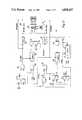
- FIG. 1is a block diagram of a computer system incorporating the present invention.
- FIG. 2is a schematic circuit diagram of a portion of the memory control circuit shown in FIG. 1.
- FIGS. 3 and 4are timing diagrams showing the signal levels at various points in the circuits of FIGS. 1 and 2 under two different memory access conditions.
- FIG. 5is a block diagram showing more particularly the type of parallel-in serial-out shift register employed in the invention.
- FIG. 6is a block diagram of another computer system incorporating the present invention.
- FIG. 7is a block diagram of still another computer system incorporating the present invention.
- a computer systemcomprises a central processing unit (CPU) 10, which may be a microprocessor, and a video display controller (VDC) 12, both of which are connected to a bi-directional data bus 15 for transmitting and receiving data to and from other components of the computer system.
- the data busis able to carry 32 digital bits in parallel and incorporates a data buffer 24.
- Both the CPU 10 and the VDC 12have address bus outputs 14 and 16, respectively, which are connected as inputs to a switch 18.
- the switch 18, when properly enabled,connects one of the two address bus outputs 14 or 16 to a main address bus 20 for the computer system.
- Both the system address bus 20 and data bus 15may be connected to other devices such as a keyboard, additional memory, mass storage devices and communication interfaces.
- the CPU 10 and VDC 12receive separate clocking signals from a system clock 26.
- the computer systemalso contains a random access memory 22 which is shown in FIG. 1 comprising separate memory banks 50-53 respectively labeled bank 0 through bank 3.
- the memory 22is connected to the system address and data buses, 20 and 15, respectively.
- the memory 22may comprise static or dynamic memory integrated circuits. Each bank is arranged so that each addressed location within the memory bank contains 32 bits of digital information. Each 32 bit memory location may be read from or written into in parallel.
- the output from each of the banks of RAM 22is fed into a separate parallel-in serial-out shift register 30-33 via connection to the system data bus 15.
- each registercomprises a respective 32-bit-wide input data latch 34 in which input data may be temporarily stored responsive to a VDC data latch signal, from which latch 34 the thirty-two consecutive stages of a respective shift register 35 may be parallelly loaded in response to a shift register load signal. The contents of respective shift register 35 may then be read out serially responsive to a serial clocking signal applied thereto.
- the combined serial outputs from the shift registers 30-33form four data bits which represent the video output (e.g. a color) for a given picture element (pixel).
- the four-bit-wide stream of data from the shift register outputsare fed to a conventional video display processor 36 the output of which is coupled to a display monitor 37.
- Display processor 36receives display synchronization signals from VDC 12 via bus 38 and relays them to monitor 37, as shown, or display synchronization signals are supplied to monitor 37 directly from VDC 12.
- the memory 22 and the shift registers 30-33are controlled by a memory controller 40 comprising both of a conventional random access memory controller 42 and a novel priority controller 44, which selects either the VDC 12 or the CPU 10 to be able to access the memory 22.
- the RAM controller 42also receives a read-write signal R/W from the CPU 10. Depending on the specific type of memory used, the controller 42 may have additional control lines running between it and the CPU 10, as is readily appreciated by one skilled in the art.
- the RAM controller 42produces RAM control signals which are fed to each of the banks of memory 22 on a RAM control bus and also produces shift register control signals on a register address bus connected to the shift registers 30-33.
- FIGS. 2, 3 and 4depict an operation of the present invention which involves a specific timing sequence.
- a video access period of 32 pixel clock pulseshas been chosen as the period during which VDP 36 under control of VDC 12 must be allowed access memory 22 in order to have data in time for display purposes.
- data for 32 pixelsare read from memory 22.
- the memory access times for both CPU 10 and VDP 36are eight clock pulses long.
- FIG. 2depicts the detailed circuitry for the priority controller 44 of FIG. 1.
- the priority controller 44receives access requests from both the CPU and the VDC on the CPU REQ and the VDC REQ lines respectively.
- the VDC REQ signallatches a first flip-flop 100 which has its output connected through node 1 to a non-inverting input of a first AND gate 102.
- the other input of the first AND gate 102is an inverting input (i.e. has an inverter connected to it) which receives a CPU enable signal, the source of which will be described subsequently.
- the output of the first AND gate 102is a VDC enable signal which is fed as one output of the priority controller 44 to the address bus switch 18 for coupling the VDC address bus 16 to the system address bus 20.
- the VDC enable signalis also connected as an input to a first delay circuit 104 which delays the VDC enable signal and provides a latched output on output line 106 to the RAM controller 42 (FIG. 1).
- the VDC data latch output on line 106indicates that the RAM 22 has now been addressed and that sufficient time has elapsed for the data to be read out of the RAM.
- the VDC enable signalis also fed as one input to a second AND gate 108 the other input of which is the clock signal at the pixel frequency from the system clock 26 (FIG. 1).
- the output of the second AND gate 108is fed as the input to a counter 110 which provides an output for every eighth input pulse.
- the counter 110is reset by the falling edge of the VDC enable pulse.
- the output of the counter 110is connected to the set input of a second flip-flop 114 which generates a VDC acknowledge signal (VDC ACK) on line 116.
- VDC ACK signal on line 116is coupled to the reset input of the first flip-flop 100.
- the pixel clock signal from clock 26is fed to the input of a second counter 124 having a latched output indicating that 18 pixel clock pulses have occurred.
- the counter 124has an unlatched second output indicating the count of 32 pixel clock pulses. This 32 count output is coupled to the reset inputs of the second flip-flop 114 and the counter 124.
- the 18 count output of the second counter 124is coupled to a non-inverting input of a fourth AND gate 126 which has an inverting input to which the VDC ACK signal from the second flip-flop 114 is coupled.
- the output of the fourth AND gate 126is coupled to an inverting input of a third AND gate 122.
- the CPU memory access request(CPU REQ) is connected as the set input of a third flip-flop 120 whose output is connected through node 2 to the non-inverting input of the third AND gate 122.
- the output of the third AND gate 122represents the CPU enable signal which, as noted above, is connected to the inverting input of the first AND gate 102.
- the CPU enable signalis also coupled to one input of a fifth AND gate 134 having another input to which the pixel clock signal is applied.
- the output of the fifth AND gate 134is connected to the input of a third counter 136 and the CPU enable signal is applied to the reset terminal of counter 136.
- the output of the third counter 136which indicates a count of eight input pulses, is coupled to the reset input of third flip-flop 120 and the set input of a fourth flip-flop 138.
- the CPU request signalis connected to the reset input of the fourth flip-flop 138.
- the output signal of the fourth flip-flopis fed back to the CPU as a CPU acknowledge signal (CPU ACK) to indicate the completion of a CPU memory access.
- CPU ACKCPU acknowledge signal
- the CPU enable signal from the third AND gate 122is supplied as an output of the priority controller 44 to the switch 18 for connecting the CPU address bus 14 to the system address bus 20.
- a second delay circuit 130has the CPU enable signal coupled to its input and provides a latched output (labeled CPU Data Latch) which is fed on line 132 to the RAM controller 42 (FIG. 1) for indicating that the address from the CPU has been fed to the RAM 22 and the data from the RAM is now ready to be read out.
- Both the CPU and the VDC data latch signalsare fed to a RAM bank enable circuit 140 which also receives at least two bits from the address bus 20.
- the RAM enable circuit 140generates an enable signal on at least one of four output lines which are connected to the enable inputs of the four RAM banks 51-53.
- FIGS. 3 and 4show a 32 pixel clock pulse time frame during which period the video display controller must access RAM 22 in order to transfer data from RAM 22 to the various shift registers 30-33 for generating a video output signal.
- the memory access by the VDC 12may occur at any period within that 32 pixel period, but must be completed by the start of the next period, in order that the shift registers 30-33 have video data to output to the video signal generator (not shown).
- the video display controller 12initiates a memory access (M VDC on timing line B) at the beginning of the first pixel clock pulse.
- M VDCmemory access
- the VDC controller 12sends a VDC request at the beginning of the first clock pulse which triggers the first flip-flop 100, FIG. 2.
- the flip-flopproduces a high input to the first AND gate 102 which, because the CPU enable signal is a low at this time, (FIG. 3, line H) causes the first AND gate 102 to produce a high VDC enable signal commencing the VDC access of video data from the RAM 22.
- the VDC enable signalis fed to the switch 18 (FIG. 1) which causes the switch to connect the VDC address bus 16 to the system address bus 20 so that the memory address is supplied from the VDC to the RAM 22.
- the VDC data latch signalis supplied on line 106 to the RAM bank enable circuit 140, which sequentially supplies a RAM enable signal on each of the four output lines connected to separate RAM banks 50-53.
- the VDC latch signal on line 106is also supplied to the RAM controller 42 which provides conventional RAM control signals to the memory 22.
- the RAM controller 42in response to the VDC data latch signal also sequentially addresses the shift registers 30-33 via the register address bus so that the various registers are enabled in a sequence corresponding to the enabling of the various RAM banks 50-53 by the priority controller 44.
- each RAM bank 50-53stores 32 bits of data at each address.
- Each of the four bits which define a given digital video pixel wordis stored in a different one of the banks. Therefore, the 32 bits stored in a given address in each RAM bank represent 32 pixels. That is, the first bit of the 32 bits stored at a given address in each RAM bank represents one of the bits in the first pixel word, the second bit at that address in each bank represents a second pixel word and so on for the 32 bits.
- the VDC memory access M VDClasts for eight pixel clock cycles, although, depending on the RAM access time, this period could vary.
- This period of eight cyclesis counted by a first counter 110, which then supplies a set signal to the second flip-flop 114.
- This set signalcauses the output of the second flip-flop 114 to go high, generating the VDC acknowledge (VDC ACK) signal on line 116 that indicates that the VDC has completed an access of the memory within the 32 pixel clock pulse frame.
- VDC ACKalso resets the first flip-flop 100, terminating the VDC enable signal.
- the CPU 10initiates a memory access (M CPU ) by generating a CPU REQ signal (line E), which is fed to the priority controller 44.
- the CPU REQsets the third flip-flop 120, producing at node 2 a high signal indicating that the CPU desires data (FIG. 3, line F).
- This request signalis supplied to one input of the second AND gate 122.
- the other input of the AND gate 122receives the output from the third AND gate 126.
- the inputs to the AND gate 126are the VDC acknowledge signal supplied to the inverting input (which signal is now high) and a low level from the 18 count output of the second counter 124. Therefore, the third AND gate 126 will at this time produce a low level output signal.
- This signal applied to the inverting input of the second AND gate 122will produce a high CPU enable signal (FIG. 3, line H).
- the high CPU enable signalcauses the switch 18 to connect the CPU address bus 14 to the system address bus 20 and generates a CPU data latch signal on line 132, after an appropriate delay in circuit 130.
- This delayed CPU data latch signalenables the CPU writing or reading of the data to or from the RAM 22.
- the CPU memory access time period M CPUis eight clock pulses wide at the end of which the third counter 136 has counted eight pixel clock pulses and emits a reset signal to the third flip-flop 120 which terminates the CPU enable signal.
- the output of the third counter 136also sets the fourth flip-flop 138 to send a memory access acknowledge signal to the CPU 10.
- a similar CPU memory accessoccurs at clock pulse 24.
- the operation of the computer system and the priority controller 44 in particularis identical to the previous CPU access.
- VDC 12initiates a request at the beginning of access period, as evidenced by the VDC REQ signal going high for the first pixel clock cycle.
- CPU 10at that instant also is requesting access to the memory, as indicated by the CPU REQ signal going high for that same clock cycle.
- the CPU request signal applied to the third flip-flop 120initiates a CPU enable signal at the output of the third AND gate 122, as was described in detail above with respect to the FIG. 3 accessing.
- This CPU enable signal going high and being applied to the first AND gate 102inhibits the VDC request from generating a high VDC enable signal, as shown on line G of FIG. 4. This inhibits the VDC 12 access to RAM 22 and enables only the CPU 10 to gain access.
- CPU 10has memory access priority.
- the output from the third counter 136resets the third flip-flop 120, terminating the CPU enable signal.
- the high level still at node 1indicates that the VDC 12 is requesting access to the memory 22 (or there is a previously requested access which is yet to be fulfilled).
- the CPU enable signalis at a low level (FIG. 4, line H)
- the first AND gate 102initiates a VDC enable signal, commencing a VDC memory access, M VDC .
- the VDCcontinues to access the memory until the beginning of clock cycle 12, at which time the CPU sends a memory request to the priority control 44.
- This CPU memory requestgenerates a high CPU enable signal, which when applied to the input of the first AND gate 102 terminates the VDC enable signal and the VDC memory access.
- the high CPU enable signalthen begins a new CPU memory access at pixel clock pulse 12, which lasts for eight clock pulses until the beginning of clock pulse 20.
- the latched high count 18 signal from counter 124 and low VDC ACK signal applied to the fourth AND gate 126generate a high output, which when fed to the inverting input of the second AND gate 122 inhibits the generation of a CPU enable signal.
- Thispermits the VDC memory access to continue for its normal duration of eight clock cycles, terminating at the completion of the twenty-seventh clock cycle. Therefore, after pixel clock cycle 18 the VDC exercises priority over memory access.
- the acknowledge signal VDC ACKgoes high, which when applied to the third AND gate 126, generates a low output.
- the low output from the third AND gate 126 applied to the inverting input of the second AND gate 122 along with the high request signal from node 2 being applied to the other inputgenerates a CPU enable signal, which commences another CPU access.
- the second counter 124At the end of clock pulse 32, the second counter 124 generates a reset signal for the second flip-flop 114, terminating the VDC acknowledge signal.
- the last CPU accessis not completed, it continues into the next 32 pixel clock pulse time frame.
- This priority schemeprovides for less restricted access to RAM 22 by CPU 10, avoiding delaying the CPU access as often for a VDC access, thus permitting improved efficiency of the CPU processing. Furthermore, this priority scheme provides for CPU 10 not having to be synchronized with the video display processor. This allows CPU 10 to run at a much higher clock frequency, to improve the speed of the CPU processing.
- FIG. 6shows a somewhat different computer system than that shown in FIG. 1, which allows CPU 10 even more freedom of access to RAM 22 than the FIG. 1 computer system. This is achieved by providing for the banks 50-53 of RAM 22 not being accessed to or from a common data bus, except as mediated by a multiplexer/buffer 25, which replaces buffer 24 of FIG. 1. Multiplexer/buffer 25 responds to the RAM enable signal, and to those bits of the address on the main address bus 20 which indicate which of banks 50-53 is selected to be written to or read from during a CPU access, to selectively connect the access port of the selected bank to data bus 15, conditioned upon CPU enable signal being provided from priority controller 44.
- This modificationallows registers 30-33 to be loaded from banks 50-53 simultaneously, rather than sequentially, during a VDC access.
- the VDC enable signalis used to select all banks 50-53 of RAM 22 for parallel read-out to their respective parallel-in/serial-out shift registers 30-33. This is done by ORing the VDC enable signal with the memory bank enable signals from priority control 44. This is done in OR gates 60-63, respectively, the output signals from OR gates 60-63 controlling the enabling of banks 50-53 of RAM 22 for read out during VDC access. So total VDC access time is reduced.
- FIG. 7shows a computer system that allows even greater freedom of access by CPU 10.
- Banks 50-53 of RAM 22have separate respective priority controllers 45-48 (shown in one box), each resembling priority controller 44.
- Banks 50-53receive their addresses from CPU 10 or from VDC 12 as separately determined by respective address switches 180-183, respectively controlled by priority controllers 45-48, rather than as determined by priority address switch 18.
- VDC enable and CPU enable signalsare shown being supplied on a single line from each of priority controllers 45-48. Responsive to the signals on these four single lines, a modified multiplexer/buffer 25' selects CPU 10 to no more one of the banks 50-53 of RAM 22.
- RAM 22is shown as having four banks 50-53 for supplying four-bit video codes to registers 30-33 for transmittal to video display processor 36.
- Video display processor 36is then presumably of a type using a color look-up table responsive to the four-bit video codes to place one of sixteen colors at each pixel location on the display screen of display monitor 37.
- This type of video display processor 36may be used with video codes having a greater number of bits, with the number of banks in RAM 22 and the number of associated parallel-in/serial-out registers being increased correspondingly.
- Increasing the number of banks in RAM 22 and the number of associated parallel-in/serial-out registers to similar higher numberwill also allow a video display processor 36 of a different type to be used. For example, twelve banks of memory may be used in RAM 22, with four bits from four associated parallel-in/serial-out registers being used to describe the red component portions of display picture elements, with five bits from four associated parallel-in/serial-out registers being used to describe the green component portions of display picture elements, and with three bits from three associated parallel-in/serial-out registers being used to describe the blue component portions of display picture elements.
Landscapes
- Engineering & Computer Science (AREA)
- Theoretical Computer Science (AREA)
- Physics & Mathematics (AREA)
- General Physics & Mathematics (AREA)
- Computer Hardware Design (AREA)
- Multimedia (AREA)
- General Engineering & Computer Science (AREA)
- Computer Graphics (AREA)
- Controls And Circuits For Display Device (AREA)
Abstract
Description
Claims (15)
Priority Applications (1)
| Application Number | Priority Date | Filing Date | Title |
|---|---|---|---|
| US07/007,536US4858107A (en) | 1985-03-11 | 1987-01-28 | Computer device display system using conditionally asynchronous memory accessing by video display controller |
Applications Claiming Priority (2)
| Application Number | Priority Date | Filing Date | Title |
|---|---|---|---|
| US71029285A | 1985-03-11 | 1985-03-11 | |
| US07/007,536US4858107A (en) | 1985-03-11 | 1987-01-28 | Computer device display system using conditionally asynchronous memory accessing by video display controller |
Related Parent Applications (2)
| Application Number | Title | Priority Date | Filing Date |
|---|---|---|---|
| US06710295Continuation-In-Part | 1985-03-11 | ||
| US71029285AContinuation-In-Part | 1985-03-11 | 1985-03-11 |
Publications (1)
| Publication Number | Publication Date |
|---|---|
| US4858107Atrue US4858107A (en) | 1989-08-15 |
Family
ID=26677114
Family Applications (1)
| Application Number | Title | Priority Date | Filing Date |
|---|---|---|---|
| US07/007,536Expired - LifetimeUS4858107A (en) | 1985-03-11 | 1987-01-28 | Computer device display system using conditionally asynchronous memory accessing by video display controller |
Country Status (1)
| Country | Link |
|---|---|
| US (1) | US4858107A (en) |
Cited By (36)
| Publication number | Priority date | Publication date | Assignee | Title |
|---|---|---|---|---|
| US5161221A (en)* | 1988-12-12 | 1992-11-03 | Eastman Kodak Company | Multi-memory bank system for receiving continuous serial data stream and monitoring same to control bank switching without interrupting continuous data flow rate |
| US5167028A (en)* | 1989-11-13 | 1992-11-24 | Lucid Corporation | System for controlling task operation of slave processor by switching access to shared memory banks by master processor |
| US5276798A (en)* | 1990-09-14 | 1994-01-04 | Hughes Aircraft Company | Multifunction high performance graphics rendering processor |
| US5299315A (en)* | 1992-09-17 | 1994-03-29 | International Business Machines Corp. | Personal computer with programmable threshold FIFO registers for data transfer |
| US5317708A (en)* | 1990-06-29 | 1994-05-31 | Digital Equipment Corporation | Apparatus and method for an improved content addressable memory |
| US5327530A (en)* | 1989-07-21 | 1994-07-05 | Samsung Electronics Co., Ltd. | Video board for serving both 1-bit plane operation and 2-bit plane operation |
| US5329615A (en)* | 1990-09-14 | 1994-07-12 | Hughes Aircraft Company | Concurrent general purpose and DMA processing in a graphics rendering processor |
| US5371849A (en)* | 1990-09-14 | 1994-12-06 | Hughes Aircraft Company | Dual hardware channels and hardware context switching in a graphics rendering processor |
| US5392391A (en)* | 1991-10-18 | 1995-02-21 | Lsi Logic Corporation | High performance graphics applications controller |
| US5440713A (en)* | 1992-05-29 | 1995-08-08 | Industrial Technology Research Institute | M-way N-port paged-interleaved memory system |
| US5459834A (en)* | 1992-08-06 | 1995-10-17 | Nec Corporation | Graphic pattern storage device using FIFO with feedback between storage stages |
| US5579458A (en)* | 1990-11-13 | 1996-11-26 | Hitachi, Ltd. | Display control system for a scan type display apparatus |
| WO1996041324A1 (en)* | 1995-06-07 | 1996-12-19 | International Business Machines Corporation | Computer system with optimized display control |
| WO1996042055A1 (en)* | 1995-06-09 | 1996-12-27 | Saab Dynamics | Memory structure |
| US5598552A (en)* | 1991-04-17 | 1997-01-28 | Sierra Semiconductor Corporation | Error free data transfers |
| US5680178A (en)* | 1988-07-13 | 1997-10-21 | Seiko Epson Corporation | Video multiplexing system for superimposition of scalable video data streams upon a background video data stream |
| US5799202A (en)* | 1990-11-19 | 1998-08-25 | Rongione; Eric | Video terminal architecture without dedicated memory |
| US5889949A (en)* | 1996-10-11 | 1999-03-30 | C-Cube Microsystems | Processing system with memory arbitrating between memory access requests in a set top box |
| GB2329985A (en)* | 1997-10-02 | 1999-04-07 | Motorola Ltd | Shared memory control method |
| US5929933A (en)* | 1988-07-13 | 1999-07-27 | Seiko Epson Corporation | Video multiplexing system for superimposition of scalable video data streams upon a background video data stream |
| US5959640A (en)* | 1996-01-23 | 1999-09-28 | Hewlett-Packard Company | Display controllers |
| FR2778258A1 (en)* | 1998-04-29 | 1999-11-05 | Texas Instruments France | Memory traffic access controller |
| WO2000041083A3 (en)* | 1999-01-08 | 2002-05-16 | Intel Corp | Method and apparatus for arbitration in a unified memory architecture |
| US20040186956A1 (en)* | 2000-01-05 | 2004-09-23 | Richard Perego | Configurable width buffered module |
| US20040256638A1 (en)* | 2000-01-05 | 2004-12-23 | Richard Perego | Configurable width buffered module having a bypass circuit |
| US20050010737A1 (en)* | 2000-01-05 | 2005-01-13 | Fred Ware | Configurable width buffered module having splitter elements |
| US20050044303A1 (en)* | 2000-01-05 | 2005-02-24 | Perego Richard E. | Memory system including an integrated circuit buffer device |
| US20050166026A1 (en)* | 2000-01-05 | 2005-07-28 | Fred Ware | Configurable width buffered module having switch elements |
| US7051151B2 (en) | 2000-01-05 | 2006-05-23 | Rambus Inc. | Integrated circuit buffer device |
| US7089620B2 (en)* | 2000-08-16 | 2006-08-15 | Senkingwerk Gmbh | Method for washing laundry in a tank-free wash path as well as wash path for carrying out the method |
| US20070088995A1 (en)* | 2005-09-26 | 2007-04-19 | Rambus Inc. | System including a buffered memory module |
| US7266634B2 (en) | 2000-01-05 | 2007-09-04 | Rambus Inc. | Configurable width buffered module having flyby elements |
| US20080080261A1 (en)* | 2005-09-26 | 2008-04-03 | Rambus Inc. | Memory system topologies including a buffer device and an integrated circuit memory device |
| US7589736B1 (en) | 2001-05-18 | 2009-09-15 | Pixelworks, Inc. | System and method for converting a pixel rate of an incoming digital image frame |
| USRE41522E1 (en) | 1995-10-20 | 2010-08-17 | Seiko Epson Corporation | Method and apparatus for scaling up and down a video image |
| US11328764B2 (en) | 2005-09-26 | 2022-05-10 | Rambus Inc. | Memory system topologies including a memory die stack |
Citations (4)
| Publication number | Priority date | Publication date | Assignee | Title |
|---|---|---|---|---|
| US4415985A (en)* | 1980-08-28 | 1983-11-15 | The Bendix Corporation | Driving circuit for cathode ray tube |
| US4595917A (en)* | 1983-06-13 | 1986-06-17 | Vectrix Corporation | Data processing technique for computer color graphic system |
| US4620186A (en)* | 1983-08-30 | 1986-10-28 | Zenith Electronics Corporation | Multi-bit write feature for video RAM |
| US4811109A (en)* | 1980-10-17 | 1989-03-07 | Canon Kabushiki Kaisha | Image processing system |
- 1987
- 1987-01-28USUS07/007,536patent/US4858107A/ennot_activeExpired - Lifetime
Patent Citations (4)
| Publication number | Priority date | Publication date | Assignee | Title |
|---|---|---|---|---|
| US4415985A (en)* | 1980-08-28 | 1983-11-15 | The Bendix Corporation | Driving circuit for cathode ray tube |
| US4811109A (en)* | 1980-10-17 | 1989-03-07 | Canon Kabushiki Kaisha | Image processing system |
| US4595917A (en)* | 1983-06-13 | 1986-06-17 | Vectrix Corporation | Data processing technique for computer color graphic system |
| US4620186A (en)* | 1983-08-30 | 1986-10-28 | Zenith Electronics Corporation | Multi-bit write feature for video RAM |
Cited By (86)
| Publication number | Priority date | Publication date | Assignee | Title |
|---|---|---|---|---|
| USRE37879E1 (en) | 1988-07-13 | 2002-10-15 | Seiko Epson Corporation | Image control device for use in a video multiplexing system for superimposition of scalable video data streams upon a background video data stream |
| US5680178A (en)* | 1988-07-13 | 1997-10-21 | Seiko Epson Corporation | Video multiplexing system for superimposition of scalable video data streams upon a background video data stream |
| US5793439A (en)* | 1988-07-13 | 1998-08-11 | Seiko Epson Corporation | Image control device for use in a video multiplexing system for superimposition of scalable video data streams upon a background video data stream |
| US5929933A (en)* | 1988-07-13 | 1999-07-27 | Seiko Epson Corporation | Video multiplexing system for superimposition of scalable video data streams upon a background video data stream |
| US5929870A (en)* | 1988-07-13 | 1999-07-27 | Seiko Epson Corporation | Video multiplexing system for superimposition of scalable video data streams upon a background video data stream |
| US5161221A (en)* | 1988-12-12 | 1992-11-03 | Eastman Kodak Company | Multi-memory bank system for receiving continuous serial data stream and monitoring same to control bank switching without interrupting continuous data flow rate |
| US5327530A (en)* | 1989-07-21 | 1994-07-05 | Samsung Electronics Co., Ltd. | Video board for serving both 1-bit plane operation and 2-bit plane operation |
| US5167028A (en)* | 1989-11-13 | 1992-11-24 | Lucid Corporation | System for controlling task operation of slave processor by switching access to shared memory banks by master processor |
| US5317708A (en)* | 1990-06-29 | 1994-05-31 | Digital Equipment Corporation | Apparatus and method for an improved content addressable memory |
| US5806083A (en)* | 1990-06-29 | 1998-09-08 | Digital Equipment Corporation | Apparatus and method for an improved content addressable memory using a random access memory to generate match information |
| US5371849A (en)* | 1990-09-14 | 1994-12-06 | Hughes Aircraft Company | Dual hardware channels and hardware context switching in a graphics rendering processor |
| US5329615A (en)* | 1990-09-14 | 1994-07-12 | Hughes Aircraft Company | Concurrent general purpose and DMA processing in a graphics rendering processor |
| US5276798A (en)* | 1990-09-14 | 1994-01-04 | Hughes Aircraft Company | Multifunction high performance graphics rendering processor |
| US5579458A (en)* | 1990-11-13 | 1996-11-26 | Hitachi, Ltd. | Display control system for a scan type display apparatus |
| US5799202A (en)* | 1990-11-19 | 1998-08-25 | Rongione; Eric | Video terminal architecture without dedicated memory |
| US5598552A (en)* | 1991-04-17 | 1997-01-28 | Sierra Semiconductor Corporation | Error free data transfers |
| US5392391A (en)* | 1991-10-18 | 1995-02-21 | Lsi Logic Corporation | High performance graphics applications controller |
| US5440713A (en)* | 1992-05-29 | 1995-08-08 | Industrial Technology Research Institute | M-way N-port paged-interleaved memory system |
| US5459834A (en)* | 1992-08-06 | 1995-10-17 | Nec Corporation | Graphic pattern storage device using FIFO with feedback between storage stages |
| US5299315A (en)* | 1992-09-17 | 1994-03-29 | International Business Machines Corp. | Personal computer with programmable threshold FIFO registers for data transfer |
| WO1996041324A1 (en)* | 1995-06-07 | 1996-12-19 | International Business Machines Corporation | Computer system with optimized display control |
| DE19616346C2 (en)* | 1995-06-07 | 2002-10-24 | Ibm | Computer system with optimized display control |
| WO1996042055A1 (en)* | 1995-06-09 | 1996-12-27 | Saab Dynamics | Memory structure |
| US6425064B2 (en) | 1995-06-09 | 2002-07-23 | Saab Dynamics | Memory structure for storage of memory vectors |
| USRE42656E1 (en) | 1995-10-20 | 2011-08-30 | Seiko Epson Corporation | Method and apparatus for scaling up and down a video image |
| USRE43641E1 (en) | 1995-10-20 | 2012-09-11 | Seiko Epson Corporation | Method and apparatus for scaling up and down a video image |
| USRE41522E1 (en) | 1995-10-20 | 2010-08-17 | Seiko Epson Corporation | Method and apparatus for scaling up and down a video image |
| US5959640A (en)* | 1996-01-23 | 1999-09-28 | Hewlett-Packard Company | Display controllers |
| US5889949A (en)* | 1996-10-11 | 1999-03-30 | C-Cube Microsystems | Processing system with memory arbitrating between memory access requests in a set top box |
| GB2329985A (en)* | 1997-10-02 | 1999-04-07 | Motorola Ltd | Shared memory control method |
| US20020194441A1 (en)* | 1998-04-29 | 2002-12-19 | Gerard Chauvel | Traffic controller using priority and burst control for reducing access latency |
| US6934820B2 (en) | 1998-04-29 | 2005-08-23 | Texas Instruments Incorporated | Traffic controller using priority and burst control for reducing access latency |
| FR2778258A1 (en)* | 1998-04-29 | 1999-11-05 | Texas Instruments France | Memory traffic access controller |
| WO2000041083A3 (en)* | 1999-01-08 | 2002-05-16 | Intel Corp | Method and apparatus for arbitration in a unified memory architecture |
| US20050223179A1 (en)* | 2000-01-05 | 2005-10-06 | Perego Richard E | Buffer device and method of operation in a buffer device |
| US7363422B2 (en) | 2000-01-05 | 2008-04-22 | Rambus Inc. | Configurable width buffered module |
| US20050156934A1 (en)* | 2000-01-05 | 2005-07-21 | Perego Richard E. | System featuring memory modules that include an integrated circuit buffer devices |
| US20050166026A1 (en)* | 2000-01-05 | 2005-07-28 | Fred Ware | Configurable width buffered module having switch elements |
| US20050041504A1 (en)* | 2000-01-05 | 2005-02-24 | Perego Richard E. | Method of operating a memory system including an integrated circuit buffer device |
| US20050193163A1 (en)* | 2000-01-05 | 2005-09-01 | Perego Richard E. | Integrated circuit buffer device |
| US20050207255A1 (en)* | 2000-01-05 | 2005-09-22 | Perego Richard E | System having a controller device, a buffer device and a plurality of memory devices |
| US20050210196A1 (en)* | 2000-01-05 | 2005-09-22 | Perego Richard E | Memory module having an integrated circuit buffer device |
| US20050044303A1 (en)* | 2000-01-05 | 2005-02-24 | Perego Richard E. | Memory system including an integrated circuit buffer device |
| US7000062B2 (en) | 2000-01-05 | 2006-02-14 | Rambus Inc. | System and method featuring a controller device and a memory module that includes an integrated circuit buffer device and a plurality of integrated circuit memory devices |
| US7003618B2 (en) | 2000-01-05 | 2006-02-21 | Rambus Inc. | System featuring memory modules that include an integrated circuit buffer devices |
| US7010642B2 (en) | 2000-01-05 | 2006-03-07 | Rambus Inc. | System featuring a controller device and a memory module that includes an integrated circuit buffer device and a plurality of integrated circuit memory devices |
| US7017002B2 (en) | 2000-01-05 | 2006-03-21 | Rambus, Inc. | System featuring a master device, a buffer device and a plurality of integrated circuit memory devices |
| US7051151B2 (en) | 2000-01-05 | 2006-05-23 | Rambus Inc. | Integrated circuit buffer device |
| US7062597B2 (en) | 2000-01-05 | 2006-06-13 | Rambus Inc. | Integrated circuit buffer device |
| US20040186956A1 (en)* | 2000-01-05 | 2004-09-23 | Richard Perego | Configurable width buffered module |
| US7200710B2 (en) | 2000-01-05 | 2007-04-03 | Rambus Inc. | Buffer device and method of operation in a buffer device |
| US7206896B2 (en) | 2000-01-05 | 2007-04-17 | Rambus Inc. | Integrated circuit buffer device |
| US7206897B2 (en) | 2000-01-05 | 2007-04-17 | Rambus Inc. | Memory module having an integrated circuit buffer device |
| US20040256638A1 (en)* | 2000-01-05 | 2004-12-23 | Richard Perego | Configurable width buffered module having a bypass circuit |
| US7266634B2 (en) | 2000-01-05 | 2007-09-04 | Rambus Inc. | Configurable width buffered module having flyby elements |
| US7320047B2 (en) | 2000-01-05 | 2008-01-15 | Rambus Inc. | System having a controller device, a buffer device and a plurality of memory devices |
| US20080034130A1 (en)* | 2000-01-05 | 2008-02-07 | Rambus Inc. | Buffered Memory Having A Control Bus And Dedicated Data Lines |
| US20050010737A1 (en)* | 2000-01-05 | 2005-01-13 | Fred Ware | Configurable width buffered module having splitter elements |
| US7356639B2 (en) | 2000-01-05 | 2008-04-08 | Rambus Inc. | Configurable width buffered module having a bypass circuit |
| US20050149662A1 (en)* | 2000-01-05 | 2005-07-07 | Perego Richard E. | System having a plurality of integrated circuit buffer devices |
| US20080109596A1 (en)* | 2000-01-05 | 2008-05-08 | Rambus Inc. | System Having A Controller Device, A Buffer Device And A Plurality Of Memory Devices |
| US7526597B2 (en) | 2000-01-05 | 2009-04-28 | Rambus Inc. | Buffered memory having a control bus and dedicated data lines |
| US7404032B2 (en) | 2000-01-05 | 2008-07-22 | Rambus Inc. | Configurable width buffered module having switch elements |
| US7523248B2 (en) | 2000-01-05 | 2009-04-21 | Rambus Inc. | System having a controller device, a buffer device and a plurality of memory devices |
| US7089620B2 (en)* | 2000-08-16 | 2006-08-15 | Senkingwerk Gmbh | Method for washing laundry in a tank-free wash path as well as wash path for carrying out the method |
| US7589736B1 (en) | 2001-05-18 | 2009-09-15 | Pixelworks, Inc. | System and method for converting a pixel rate of an incoming digital image frame |
| US7893943B1 (en) | 2001-05-18 | 2011-02-22 | Pixelworks, Inc. | Systems and methods for converting a pixel rate of an incoming digital image frame |
| US7729151B2 (en) | 2005-09-26 | 2010-06-01 | Rambus Inc. | System including a buffered memory module |
| US9117035B2 (en) | 2005-09-26 | 2015-08-25 | Rambus Inc. | Memory system topologies including a buffer device and an integrated circuit memory device |
| US7464225B2 (en) | 2005-09-26 | 2008-12-09 | Rambus Inc. | Memory module including a plurality of integrated circuit memory devices and a plurality of buffer devices in a matrix topology |
| US20080080261A1 (en)* | 2005-09-26 | 2008-04-03 | Rambus Inc. | Memory system topologies including a buffer device and an integrated circuit memory device |
| US7562271B2 (en) | 2005-09-26 | 2009-07-14 | Rambus Inc. | Memory system topologies including a buffer device and an integrated circuit memory device |
| US20070088995A1 (en)* | 2005-09-26 | 2007-04-19 | Rambus Inc. | System including a buffered memory module |
| US8108607B2 (en) | 2005-09-26 | 2012-01-31 | Rambus Inc. | Memory system topologies including a buffer device and an integrated circuit memory device |
| US20080144411A1 (en)* | 2005-09-26 | 2008-06-19 | Rambus Inc. | Memory Module Including A Plurality Of Integrated Circuit Memory Devices And A Plurality Of Buffer Devices In A Matrix Topology |
| US8539152B2 (en) | 2005-09-26 | 2013-09-17 | Rambus Inc. | Memory system topologies including a buffer device and an integrated circuit memory device |
| US7685364B2 (en) | 2005-09-26 | 2010-03-23 | Rambus Inc. | Memory system topologies including a buffer device and an integrated circuit memory device |
| US9563583B2 (en) | 2005-09-26 | 2017-02-07 | Rambus Inc. | Memory system topologies including a buffer device and an integrated circuit memory device |
| US9865329B2 (en) | 2005-09-26 | 2018-01-09 | Rambus Inc. | Memory system topologies including a buffer device and an integrated circuit memory device |
| US10381067B2 (en) | 2005-09-26 | 2019-08-13 | Rambus Inc. | Memory system topologies including a buffer device and an integrated circuit memory device |
| US10535398B2 (en) | 2005-09-26 | 2020-01-14 | Rambus Inc. | Memory system topologies including a buffer device and an integrated circuit memory device |
| US10672458B1 (en) | 2005-09-26 | 2020-06-02 | Rambus Inc. | Memory system topologies including a buffer device and an integrated circuit memory device |
| US11043258B2 (en) | 2005-09-26 | 2021-06-22 | Rambus Inc. | Memory system topologies including a memory die stack |
| US11328764B2 (en) | 2005-09-26 | 2022-05-10 | Rambus Inc. | Memory system topologies including a memory die stack |
| US11727982B2 (en) | 2005-09-26 | 2023-08-15 | Rambus Inc. | Memory system topologies including a memory die stack |
| US12394471B2 (en) | 2005-09-26 | 2025-08-19 | Rambus Inc. | Memory system topologies including a memory die stack |
Similar Documents
| Publication | Publication Date | Title |
|---|---|---|
| US4858107A (en) | Computer device display system using conditionally asynchronous memory accessing by video display controller | |
| RU2134447C1 (en) | Data transfer device and video game using it | |
| US4511965A (en) | Video ram accessing system | |
| US5793996A (en) | Bridge for interconnecting a computer system bus, an expansion bus and a video frame buffer | |
| US4818932A (en) | Concurrent memory access system | |
| US7019751B2 (en) | Graphic processing apparatus and method | |
| EP0082683A2 (en) | Computer memory system | |
| EP0188828A2 (en) | Image processing apparatus and intercommunication bus therefor | |
| AU602062B2 (en) | Video apparatus employing vrams | |
| JP2878022B2 (en) | Display system | |
| JPH011027A (en) | a video device that provides video data to a display device | |
| GB2137857A (en) | Computer Graphics System | |
| US5634013A (en) | Bus bridge address translator | |
| JPH0622008B2 (en) | Synchronization circuit | |
| US4591845A (en) | Character and graphic signal generating apparatus | |
| US4581611A (en) | Character display system | |
| JPH0792779B2 (en) | Data transfer controller | |
| EP0264603A2 (en) | Raster scan digital display system | |
| US4901062A (en) | Raster scan digital display system | |
| JPH02150976A (en) | Easy to upgrade video memory system and method therefor | |
| JPS58169390A (en) | Writing for buffer memory | |
| JPS6048828B2 (en) | Memory addressing method | |
| JPS61208553A (en) | Computer access control method and apparatus | |
| JPS58184188A (en) | Reading and writting system of display data | |
| JP2780857B2 (en) | Image display device |
Legal Events
| Date | Code | Title | Description |
|---|---|---|---|
| AS | Assignment | Owner name:RCA CORPORATION, A CORP. OF DE Free format text:ASSIGNMENT OF ASSIGNORS INTEREST.;ASSIGNOR:FEDELE, NICOLA J.;REEL/FRAME:004665/0053 Effective date:19870122 | |
| AS | Assignment | Owner name:GENERAL ELECTRIC COMPANY Free format text:MERGER;ASSIGNOR:R C A CORPORATION, A CORP. OF DE.;REEL/FRAME:004837/0618 Effective date:19880129 Owner name:GENERAL ELECTRIC COMPANY,STATELESS Free format text:MERGER;ASSIGNOR:R C A CORPORATION, A CORP. OF DE.;REEL/FRAME:004837/0618 Effective date:19880129 | |
| FEPP | Fee payment procedure | Free format text:PAYOR NUMBER ASSIGNED (ORIGINAL EVENT CODE: ASPN); ENTITY STATUS OF PATENT OWNER: LARGE ENTITY | |
| STCF | Information on status: patent grant | Free format text:PATENTED CASE | |
| FEPP | Fee payment procedure | Free format text:PAYER NUMBER DE-ASSIGNED (ORIGINAL EVENT CODE: RMPN); ENTITY STATUS OF PATENT OWNER: LARGE ENTITY Free format text:PAYOR NUMBER ASSIGNED (ORIGINAL EVENT CODE: ASPN); ENTITY STATUS OF PATENT OWNER: LARGE ENTITY | |
| FPAY | Fee payment | Year of fee payment:4 | |
| FPAY | Fee payment | Year of fee payment:8 | |
| FPAY | Fee payment | Year of fee payment:12 |