US4856544A - Vessel and system for treating wafers with fluids - Google Patents
Vessel and system for treating wafers with fluidsDownload PDFInfo
- Publication number
- US4856544A US4856544AUS07/125,245US12524587AUS4856544AUS 4856544 AUS4856544 AUS 4856544AUS 12524587 AUS12524587 AUS 12524587AUS 4856544 AUS4856544 AUS 4856544A
- Authority
- US
- United States
- Prior art keywords
- wafers
- vessels
- fluid
- vessel
- treatment
- Prior art date
- Legal status (The legal status is an assumption and is not a legal conclusion. Google has not performed a legal analysis and makes no representation as to the accuracy of the status listed.)
- Expired - Lifetime
Links
- 235000012431wafersNutrition0.000titleclaimsabstractdescription119
- 239000012530fluidSubstances0.000titleclaimsabstractdescription78
- 239000004065semiconductorSubstances0.000claimsabstractdescription21
- 239000007788liquidSubstances0.000claimsdescription20
- 238000007789sealingMethods0.000claimsdescription12
- 239000000463materialSubstances0.000abstractdescription9
- 238000004140cleaningMethods0.000abstractdescription8
- 238000000034methodMethods0.000description12
- 239000000969carrierSubstances0.000description11
- 239000000243solutionSubstances0.000description11
- KRHYYFGTRYWZRS-UHFFFAOYSA-NFluoraneChemical compoundFKRHYYFGTRYWZRS-UHFFFAOYSA-N0.000description10
- QAOWNCQODCNURD-UHFFFAOYSA-NSulfuric acidChemical compoundOS(O)(=O)=OQAOWNCQODCNURD-UHFFFAOYSA-N0.000description10
- 238000013461designMethods0.000description10
- XLYOFNOQVPJJNP-UHFFFAOYSA-NwaterSubstancesOXLYOFNOQVPJJNP-UHFFFAOYSA-N0.000description9
- IJGRMHOSHXDMSA-UHFFFAOYSA-NAtomic nitrogenChemical compoundN#NIJGRMHOSHXDMSA-UHFFFAOYSA-N0.000description8
- 239000003153chemical reaction reagentSubstances0.000description8
- 238000011109contaminationMethods0.000description7
- 238000012545processingMethods0.000description7
- 229910021642ultra pure waterInorganic materials0.000description7
- 239000012498ultrapure waterSubstances0.000description7
- 238000009792diffusion processMethods0.000description6
- 230000013011matingEffects0.000description6
- 230000008569processEffects0.000description6
- 239000002253acidSubstances0.000description5
- 230000000694effectsEffects0.000description4
- 239000012535impuritySubstances0.000description4
- 229910052757nitrogenInorganic materials0.000description4
- OKKJLVBELUTLKV-UHFFFAOYSA-NMethanolChemical compoundOCOKKJLVBELUTLKV-UHFFFAOYSA-N0.000description3
- 230000009471actionEffects0.000description3
- 239000000356contaminantSubstances0.000description3
- 238000001035dryingMethods0.000description3
- 238000005530etchingMethods0.000description3
- 229920002313fluoropolymerPolymers0.000description3
- 238000004519manufacturing processMethods0.000description3
- 239000007800oxidant agentSubstances0.000description3
- 239000002245particleSubstances0.000description3
- 239000011295pitchSubstances0.000description3
- 230000003068static effectEffects0.000description3
- 239000000126substanceSubstances0.000description3
- 238000011144upstream manufacturingMethods0.000description3
- CURLTUGMZLYLDI-UHFFFAOYSA-NCarbon dioxideChemical compoundO=C=OCURLTUGMZLYLDI-UHFFFAOYSA-N0.000description2
- 230000001154acute effectEffects0.000description2
- 230000008901benefitEffects0.000description2
- 230000006835compressionEffects0.000description2
- 238000007906compressionMethods0.000description2
- 239000003517fumeSubstances0.000description2
- 238000011068loading methodMethods0.000description2
- 239000002184metalSubstances0.000description2
- 229910052751metalInorganic materials0.000description2
- 150000002739metalsChemical class0.000description2
- 238000002156mixingMethods0.000description2
- 238000012986modificationMethods0.000description2
- 230000004048modificationEffects0.000description2
- 229920002120photoresistant polymerPolymers0.000description2
- LFQSCWFLJHTTHZ-UHFFFAOYSA-NEthanolChemical compoundCCOLFQSCWFLJHTTHZ-UHFFFAOYSA-N0.000description1
- 229920002449FKMPolymers0.000description1
- CBENFWSGALASAD-UHFFFAOYSA-NOzoneChemical compound[O-][O+]=OCBENFWSGALASAD-UHFFFAOYSA-N0.000description1
- 239000004809TeflonSubstances0.000description1
- 229920006362Teflon®Polymers0.000description1
- 239000012042active reagentSubstances0.000description1
- 230000006978adaptationEffects0.000description1
- 239000000853adhesiveSubstances0.000description1
- 230000001070adhesive effectEffects0.000description1
- 229910002092carbon dioxideInorganic materials0.000description1
- 239000001569carbon dioxideSubstances0.000description1
- 238000005266castingMethods0.000description1
- 239000000919ceramicSubstances0.000description1
- 239000003795chemical substances by applicationSubstances0.000description1
- 239000012141concentrateSubstances0.000description1
- 238000010276constructionMethods0.000description1
- 239000012050conventional carrierSubstances0.000description1
- 230000007423decreaseEffects0.000description1
- 238000006073displacement reactionMethods0.000description1
- 239000002019doping agentSubstances0.000description1
- 239000000428dustSubstances0.000description1
- 229920001971elastomerPolymers0.000description1
- 239000000806elastomerSubstances0.000description1
- 239000004811fluoropolymerSubstances0.000description1
- 239000007789gasSubstances0.000description1
- 239000012456homogeneous solutionSubstances0.000description1
- -1i.e.Substances0.000description1
- 238000007654immersionMethods0.000description1
- 230000006872improvementEffects0.000description1
- 238000002347injectionMethods0.000description1
- 239000007924injectionSubstances0.000description1
- 238000003754machiningMethods0.000description1
- 238000012423maintenanceMethods0.000description1
- 238000003913materials processingMethods0.000description1
- 230000007246mechanismEffects0.000description1
- 239000000203mixtureSubstances0.000description1
- 238000000465mouldingMethods0.000description1
- 239000003921oilSubstances0.000description1
- 230000003647oxidationEffects0.000description1
- 238000007254oxidation reactionMethods0.000description1
- 239000004033plasticSubstances0.000description1
- 229920003023plasticPolymers0.000description1
- 239000004810polytetrafluoroethyleneSubstances0.000description1
- 229940058401polytetrafluoroethyleneDrugs0.000description1
- 238000002360preparation methodMethods0.000description1
- 230000009467reductionEffects0.000description1
- 238000006722reduction reactionMethods0.000description1
- 230000000717retained effectEffects0.000description1
- 230000002441reversible effectEffects0.000description1
- 239000007787solidSubstances0.000description1
- 239000002904solventSubstances0.000description1
- 238000004544sputter depositionMethods0.000description1
- 230000007704transitionEffects0.000description1
- 238000005406washingMethods0.000description1
- 239000002699waste materialSubstances0.000description1
- 238000001039wet etchingMethods0.000description1
- 238000009736wettingMethods0.000description1
Images


Classifications
- H—ELECTRICITY
- H01—ELECTRIC ELEMENTS
- H01L—SEMICONDUCTOR DEVICES NOT COVERED BY CLASS H10
- H01L21/00—Processes or apparatus adapted for the manufacture or treatment of semiconductor or solid state devices or of parts thereof
- H01L21/67—Apparatus specially adapted for handling semiconductor or electric solid state devices during manufacture or treatment thereof; Apparatus specially adapted for handling wafers during manufacture or treatment of semiconductor or electric solid state devices or components ; Apparatus not specifically provided for elsewhere
- H01L21/67005—Apparatus not specifically provided for elsewhere
- H01L21/67011—Apparatus for manufacture or treatment
- H01L21/67017—Apparatus for fluid treatment
- H01L21/67028—Apparatus for fluid treatment for cleaning followed by drying, rinsing, stripping, blasting or the like
- H01L21/6704—Apparatus for fluid treatment for cleaning followed by drying, rinsing, stripping, blasting or the like for wet cleaning or washing
- H01L21/67051—Apparatus for fluid treatment for cleaning followed by drying, rinsing, stripping, blasting or the like for wet cleaning or washing using mainly spraying means, e.g. nozzles
- B—PERFORMING OPERATIONS; TRANSPORTING
- B05—SPRAYING OR ATOMISING IN GENERAL; APPLYING FLUENT MATERIALS TO SURFACES, IN GENERAL
- B05C—APPARATUS FOR APPLYING FLUENT MATERIALS TO SURFACES, IN GENERAL
- B05C3/00—Apparatus in which the work is brought into contact with a bulk quantity of liquid or other fluent material
- B05C3/02—Apparatus in which the work is brought into contact with a bulk quantity of liquid or other fluent material the work being immersed in the liquid or other fluent material
- B05C3/09—Apparatus in which the work is brought into contact with a bulk quantity of liquid or other fluent material the work being immersed in the liquid or other fluent material for treating separate articles
- B05C3/109—Passing liquids or other fluent materials into or through chambers containing stationary articles
- B—PERFORMING OPERATIONS; TRANSPORTING
- B08—CLEANING
- B08B—CLEANING IN GENERAL; PREVENTION OF FOULING IN GENERAL
- B08B7/00—Cleaning by methods not provided for in a single other subclass or a single group in this subclass
- B08B7/0064—Cleaning by methods not provided for in a single other subclass or a single group in this subclass by temperature changes
- B08B7/0092—Cleaning by methods not provided for in a single other subclass or a single group in this subclass by temperature changes by cooling
- C—CHEMISTRY; METALLURGY
- C23—COATING METALLIC MATERIAL; COATING MATERIAL WITH METALLIC MATERIAL; CHEMICAL SURFACE TREATMENT; DIFFUSION TREATMENT OF METALLIC MATERIAL; COATING BY VACUUM EVAPORATION, BY SPUTTERING, BY ION IMPLANTATION OR BY CHEMICAL VAPOUR DEPOSITION, IN GENERAL; INHIBITING CORROSION OF METALLIC MATERIAL OR INCRUSTATION IN GENERAL
- C23C—COATING METALLIC MATERIAL; COATING MATERIAL WITH METALLIC MATERIAL; SURFACE TREATMENT OF METALLIC MATERIAL BY DIFFUSION INTO THE SURFACE, BY CHEMICAL CONVERSION OR SUBSTITUTION; COATING BY VACUUM EVAPORATION, BY SPUTTERING, BY ION IMPLANTATION OR BY CHEMICAL VAPOUR DEPOSITION, IN GENERAL
- C23C16/00—Chemical coating by decomposition of gaseous compounds, without leaving reaction products of surface material in the coating, i.e. chemical vapour deposition [CVD] processes
- C23C16/44—Chemical coating by decomposition of gaseous compounds, without leaving reaction products of surface material in the coating, i.e. chemical vapour deposition [CVD] processes characterised by the method of coating
- C23C16/54—Apparatus specially adapted for continuous coating
- C—CHEMISTRY; METALLURGY
- C30—CRYSTAL GROWTH
- C30B—SINGLE-CRYSTAL GROWTH; UNIDIRECTIONAL SOLIDIFICATION OF EUTECTIC MATERIAL OR UNIDIRECTIONAL DEMIXING OF EUTECTOID MATERIAL; REFINING BY ZONE-MELTING OF MATERIAL; PRODUCTION OF A HOMOGENEOUS POLYCRYSTALLINE MATERIAL WITH DEFINED STRUCTURE; SINGLE CRYSTALS OR HOMOGENEOUS POLYCRYSTALLINE MATERIAL WITH DEFINED STRUCTURE; AFTER-TREATMENT OF SINGLE CRYSTALS OR A HOMOGENEOUS POLYCRYSTALLINE MATERIAL WITH DEFINED STRUCTURE; APPARATUS THEREFOR
- C30B33/00—After-treatment of single crystals or homogeneous polycrystalline material with defined structure
- H—ELECTRICITY
- H01—ELECTRIC ELEMENTS
- H01L—SEMICONDUCTOR DEVICES NOT COVERED BY CLASS H10
- H01L21/00—Processes or apparatus adapted for the manufacture or treatment of semiconductor or solid state devices or of parts thereof
- H01L21/67—Apparatus specially adapted for handling semiconductor or electric solid state devices during manufacture or treatment thereof; Apparatus specially adapted for handling wafers during manufacture or treatment of semiconductor or electric solid state devices or components ; Apparatus not specifically provided for elsewhere
- H01L21/67005—Apparatus not specifically provided for elsewhere
- H01L21/67011—Apparatus for manufacture or treatment
- H01L21/67017—Apparatus for fluid treatment
- H01L21/67028—Apparatus for fluid treatment for cleaning followed by drying, rinsing, stripping, blasting or the like
- H01L21/6704—Apparatus for fluid treatment for cleaning followed by drying, rinsing, stripping, blasting or the like for wet cleaning or washing
- H01L21/67057—Apparatus for fluid treatment for cleaning followed by drying, rinsing, stripping, blasting or the like for wet cleaning or washing with the semiconductor substrates being dipped in baths or vessels
- H—ELECTRICITY
- H01—ELECTRIC ELEMENTS
- H01L—SEMICONDUCTOR DEVICES NOT COVERED BY CLASS H10
- H01L21/00—Processes or apparatus adapted for the manufacture or treatment of semiconductor or solid state devices or of parts thereof
- H01L21/67—Apparatus specially adapted for handling semiconductor or electric solid state devices during manufacture or treatment thereof; Apparatus specially adapted for handling wafers during manufacture or treatment of semiconductor or electric solid state devices or components ; Apparatus not specifically provided for elsewhere
- H01L21/677—Apparatus specially adapted for handling semiconductor or electric solid state devices during manufacture or treatment thereof; Apparatus specially adapted for handling wafers during manufacture or treatment of semiconductor or electric solid state devices or components ; Apparatus not specifically provided for elsewhere for conveying, e.g. between different workstations
- H01L21/67739—Apparatus specially adapted for handling semiconductor or electric solid state devices during manufacture or treatment thereof; Apparatus specially adapted for handling wafers during manufacture or treatment of semiconductor or electric solid state devices or components ; Apparatus not specifically provided for elsewhere for conveying, e.g. between different workstations into and out of processing chamber
- H01L21/67754—Apparatus specially adapted for handling semiconductor or electric solid state devices during manufacture or treatment thereof; Apparatus specially adapted for handling wafers during manufacture or treatment of semiconductor or electric solid state devices or components ; Apparatus not specifically provided for elsewhere for conveying, e.g. between different workstations into and out of processing chamber horizontal transfer of a batch of workpieces
- H—ELECTRICITY
- H01—ELECTRIC ELEMENTS
- H01L—SEMICONDUCTOR DEVICES NOT COVERED BY CLASS H10
- H01L21/00—Processes or apparatus adapted for the manufacture or treatment of semiconductor or solid state devices or of parts thereof
- H01L21/67—Apparatus specially adapted for handling semiconductor or electric solid state devices during manufacture or treatment thereof; Apparatus specially adapted for handling wafers during manufacture or treatment of semiconductor or electric solid state devices or components ; Apparatus not specifically provided for elsewhere
- H01L21/677—Apparatus specially adapted for handling semiconductor or electric solid state devices during manufacture or treatment thereof; Apparatus specially adapted for handling wafers during manufacture or treatment of semiconductor or electric solid state devices or components ; Apparatus not specifically provided for elsewhere for conveying, e.g. between different workstations
- H01L21/67763—Apparatus specially adapted for handling semiconductor or electric solid state devices during manufacture or treatment thereof; Apparatus specially adapted for handling wafers during manufacture or treatment of semiconductor or electric solid state devices or components ; Apparatus not specifically provided for elsewhere for conveying, e.g. between different workstations the wafers being stored in a carrier, involving loading and unloading
- H01L21/67778—Apparatus specially adapted for handling semiconductor or electric solid state devices during manufacture or treatment thereof; Apparatus specially adapted for handling wafers during manufacture or treatment of semiconductor or electric solid state devices or components ; Apparatus not specifically provided for elsewhere for conveying, e.g. between different workstations the wafers being stored in a carrier, involving loading and unloading involving loading and unloading of wafers
- H01L21/67781—Batch transfer of wafers
- Y—GENERAL TAGGING OF NEW TECHNOLOGICAL DEVELOPMENTS; GENERAL TAGGING OF CROSS-SECTIONAL TECHNOLOGIES SPANNING OVER SEVERAL SECTIONS OF THE IPC; TECHNICAL SUBJECTS COVERED BY FORMER USPC CROSS-REFERENCE ART COLLECTIONS [XRACs] AND DIGESTS
- Y10—TECHNICAL SUBJECTS COVERED BY FORMER USPC
- Y10S—TECHNICAL SUBJECTS COVERED BY FORMER USPC CROSS-REFERENCE ART COLLECTIONS [XRACs] AND DIGESTS
- Y10S134/00—Cleaning and liquid contact with solids
- Y10S134/902—Semiconductor wafer
Definitions
- This inventionrelates to materials processing. More particularly, it relates to teatment of wafers such as semiconductor wafers with liquid or gaseous fluids.
- Pre-diffusion cleaningis a good example of a step in the process of fabricating semiconductor wafers which must be carefully controlled to avoid contamination. Since the diffusion step in semiconductor processing is intended to "drive-in" desired dopant atoms through high temperature exposure, any contaminants left on the wafer surface after cleaning may also be driven into the wafer and can result in faulty electrical properties.
- Pre-diffusion cleaningconventionally is accomplished by loading the wafers into a basket, such as the baskets described in U.S. Pat. Nos. 3,923,156 and 3,926,305, and then immersing the wafers and basket in a series of open sinks or tank baths.
- a strong oxidizing agentsuch as sulfuric acid
- rinsingwith water
- an etchantsuch as hydrofluoric acid
- Open baths mounted in countertopspose significant safety problems to technicians who may be exposed to the active reagents or their fumes.
- airborne impuritiescan and do contaminate the reagents and rinse water, leading to reduced semiconductor yields.
- a simple, efficient system for treating semiconductor wafers with fluidsresides in a vessel which serves to store a plurality of the wafers while at the same time serving as the walls of a treatment fluid flow line.
- a vesselpermits the fluid treatment processes to be carried out in a totally enclosed manner, thereby avoiding safety and contamination problems.
- the vesselmay be designed to ensure that all of the wafers are properly exposed to the fluid, turbulence or eddy currents are minimized, and pockets where residual contaminates may collect are eliminated.
- the concept of the inventionis to provide a semiconductor wafer treatment vessel which may be used singly, or in series with other similar or identical vessels, to form an integral part of a wafer treatment fluid flow line.
- the vessels and fluid lines gaskets, connectors and other parts of the systemare preferably fabricated from materials which are inert to the treatment fluid, e.g., fluorinated polymers.
- the vesselsare designed to avoid any pockets or recesses where spent fluid solutes or particulates removed from one batch of the wafers may collect or be temporarily retained only to contaminate the next batch, and to avoid creation of fluid flow peculiarities which might serve to concentrate solutes.
- microcrackswhere parts join, interior acute angles and other sharp corners, and recesses are avoided so that all treatment fluid flows through the vessel and is transported away to be discarded or repurified.
- the inventioncontemplates an automated system wherein plural vessels incorporated within a fluid flow line are loaded with wafers, or with a conventional carrier containing a plurality of wafers, e.g., through a sealable opening disposed in a lateral wall of each vessel. A series of fluid processing steps may then be carried out in sequence without the need to move the wafers from one bath to another.
- the inventionprovides a semiconductor treatment station disposed in a fluid flow line.
- the stationcomprises a single wafer vessel, or plural wafer vessels arranged serially, which consist of opposed lateral walls disposed about an axis parallel to the direction of fluid flow defining a fluid-tight compartment having opposed open ends.
- Each vesselincludes internal structure for supporting a plurality of planar wafers, oriented with the plane of the wafers parallel to the flow axis.
- the wafersare contained in a wafer carrier.
- Each vesselhas a sealable opening, defined by at least a portion of at least one of the lateral walls, which permits the introduction and withdrawal of the wafers, and may be sealed by means of a panel, door or the like.
- a fluid inletis disposed at one open end of the vessel or series of vessels, and a fluid outlet is disposed at the opposite end.
- the inlet and outletare connected to fluid conduits, which in turn are connected to one or more sources of treatment fluid, one or more spent fluid drains, or means for reclaiming fluids for reuse.
- sequential treatment stepsmay involve reversing the direction of fluid flow, in which case the inlet and outlet reverse rolls.
- the vesselsinclude internally disposed structure for nesting a wafer carrier in a selected position therewithin.
- the inletincludes an expander which expands the cross-section fluid flow from the narrow flow lines to the larger dimensions of the vessels.
- the dimensions of the inlet and outletare substantially coextensive with the dimensions of the open ends of the vessels.
- a means for imparting plug flow to a liquid introduced into the vessels through the expander to displace another liquid contained in the vesselsis preferably included upstream of the expander.
- the plug flow imparting meanspreferably takes the form of a 360° helix disposed immediately upstream of the expander.
- each vesseldefines an enclosure having lateral walls defining opposed open ends.
- One or more horizontal bars or other protrusions from the interior side walls of the vesselsupport a wafer carrier within the vessel.
- the vesselincludes structure for locating the wafer carrier in a selected position within the vessel.
- Sealing meanse.g., elastomeric gaskets, are disposed about one or both open ends of each of the vessels so that each vessel may be sealingly engaged with another, with a fluid inlet, or with a fluid outlet.
- the vesselsmay be sealed together by pneumatically compressing the elastomeric gaskets.
- an expanderfits onto a terminal vessel and serves to expand the cross-sectional flow area of treatment fluid as it is introduced into the vessels so that each of the wafers is fully exposed.
- a flow diverting surfacesuch as a 360° helix disposed upstream of the expander is employed to aid in expansion of the cross-sectional fluid flow as it passes through the expander. This results in "plug flow" of a liquid introduced into the vessels to displace another.
- the opposite terminal vesselmay be sealed to an extractor which serves to reduce the fluid flow from the cross-sectional dimensions of the vessels to those of the fluid flow line so that the treatment fluid can be removed while minimizing turbulent flow and eddy currents.
- the apparatusis designed such that the direction of fluid flow can be reversed. In that case the expander and extractor exchange roles.
- the system described abovepermits hydraulically full, high flow circulation, assures uniform, full contact wetting, reduces reagent consumption, prevents back eddy currents of impurities and filming effects during etching, leads to more consistent localized acid concentrations, and generally results in more consistent, uniform treatment and improved semiconductor yields. Furthermore, because the operation is totally enclosed, the intrusion of airborne contaminants and carbon dioxide is eliminated, and there is no danger of operator exposure to dangerous chemicals. Such treatment stations may be used to conduct pre-diffusion cleaning, rinsing, etching and other batch operations including drying. Furthermore, use of the invention decreases handling and permits tighter control of treatment time, temperature, and endpoint conductivity.
- FIG. 1Bis a top plan view of the vessel of FIG. 1A;
- FIG. 1Cis a cross-sectional view of two vessels of the type shown in FIG. 1A shown in serial, sealing engagement;
- FIG. 2Ais a perspective view of a second embodiment of the vessel of the invention showing a lift for gently nesting a wafer carrier therewithin;
- FIG. 2Bis a top plan view of the vessel of FIG. 2A;
- FIG. 3is a perspective view of a third embodiment of the invention illustrating an expander and extractor connected to a fluid flow line and to a two-compartment vessel having a panel fitted with wafer carrier supports;
- FIG. 4is a perspective view of a fourth embodiment of the vessel of the invention showing two wafer carriers disposed therein;
- FIG. 5is a perspective, partly broken-away view of a fifth embodiment of the invention similar to that of FIG. 4, but adapted to receive plural individual wafers instead of a wafer carrier;
- FIG. 6is a schematic cross-sectional illustration of an embodiment of a system of the invention including an exemplary treatment station comprising a two-compartment vessel constructed in accordance with the invention.
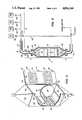
- vessels 10comprising two side walls 12 and two end walls 14.
- the wallsdefine an enclosure disposed about axis 19 having a top opening 13a opposing a bottom opening 13b.
- Each vessel 10also includes, for supporting and positioning a wafer carrier schematically illustrated at 16, structure comprising corner mounted positioning bars 17 and support bars 18 extending between walls 12. The surfaces of positioning bars 17 and supports bars 18 cooperate to hold the wafer carrier 16 in position.
- Wafer carrier 16supports a plurality of semiconductor wafers (not shown) in aligned, parallel, spaced-apart relation to one another. the vessel and the wafer carrier for use therein will typically be designed to hold 25 wafers.
- the top of the vessel 10includes a chamfered or beveled edge 22 and an elastomeric gasket 24.
- the beveled edge 22 and gasket 24 on the top of vessel 10are designed to interconnect with interfitting beveled edge 26 and surface 27 on the bottom of a vessel of similar, preferably identical design, as shown in FIG. 1C.
- FIG. 1CThe interconnection of the vessels are illustrated in FIG. 1C, wherein two vessels 10a and 10b are shown in cross section nested together.
- the chamfered top edge 22 of vessel 10b and beveled bottom 26 of vessel 10aare shown in engagement.
- Gasket 24is held in position by slots formed in the top of lateral walls 12 and 14.
- beveled edges 22 and 26interfit, and gasket 24 is urged against surface 27 to form a fluid-tight seal between the vessels.
- the sealsbulge slightly inwardly toward the wafers so that pockets where fluid might collect are eliminated.
- Beveled edge 22 and gasket 24 of vessel 10acan interfit with another vessel (not shown), of the same or a different design, having an interfitting bevel and sealing surface like those illustrated at 26 and 27. Also, one or more additional vessels may be nested below vessel 10b and will have appropriate interfitting sealing means for mating with surfaces 26 and 27.
- the terminal vessels in a series of nested vesselssuch as is depicted in FIG. 1C comprise sealing means for sealing interconnection with a wafer treatment fluid inlet and a wafer treatment fluid outlet, or structure communicating with the inlet and outlet.
- the sealsmay comprise and preferably do comprise the same structure of interfitting chamfered edges, gasket, and surfaces as are employed in interconnecting the vessels.
- the fluid inlet and outlet used to urge a hydraulically full flow of fluid in a direction parallel to flow axis 19will have mating parts for sealingly engaging the assembled vessels.
- an expander 40illustrated in FIG. 6 will have a lower mating edge comprising a beveled surface and a sealing surface identical to the surfaces 26 and 27 on vessel 10b of FIG. 1C.
- An extractor 48(illustrated in FIG. 6) will have a upper mating edge comprising a beveled edge and gasket identical to surface 22 and gasket 24 on vessel 10b of FIG. 1C.
- gasket 24is shown fixed to the top edge of the vessels 10, it should be clear that the gasket may also be carried by the bottom edge and that various other interconnecting edge arrangements can be designed by those skilled in the art.
- the object in any such designshould be to assure sealing engagement between the mating parts and to facilitate automated loading, interfitting, and other manipulation of the vessels.
- FIGS. 2A and 2Bshow an alternative embodiment 11 of a vessel constructed in accordance with the invention. Like the vessel of FIGS. 1A, 1B, and 1C, it comprises lateral sidewalls 12 and endwalls 14 defining an enclosure for a wafer carrier, and includes internally disposed wafer carrier positioning bars 17. However, in place of the wafer support bars extending across the internal diameter of the vessel are hanging supports 15 protruding from sidewalls 12 below the upper open end 13a of the vessel 11. These serve to support a wafer carrier containing wafers (not shown) which rests on the top surface of supports 15 and is suspended within the vessel 11.
- FIGS. 2A and 2Balso illustrate an exemplary device for placing a loaded wafer carrier within a vessel of the invention. It comprises a hydraulic cylinder 30, serviced by hydraulic fluid lines 31, which imparts linear motion to a hydraulic piston 32 and its associated wafer-supporting platform 34. With the piston extended as shown in FIG. 2A a wafer carrier is rested on platform 34, then cylinder 30 is actuated to lower the platform and the carrier into the vessel 11, thereby positioning the carrier between positioning bars 17 and suspending it on supports 15. After the vessel has been placed in line as disclosed hereinafter and the wafers have been treated, the carrier loaded with wafers may be removed by the hydraulic piston 32 by reversing the procedure just described.
- FIGS. 1 and 2After being loaded with wafer carriers containing wafers, are used singly or engage with other vessels as shown in FIG. 1C, and then connected to an expander and extractor as illustrated in FIG. 6 to form fluid-tight seals between the various mating parts.
- This stepmay conveniently be accomplished by means of a hydralic or pneumatic press (not shown) which holds the vessels in compression during processing of the wafers. After processing, the press serves to gently separate the vessel or vessels from their connection with the expander, extractor, and fluid flow lines to permit removal of the vessel and unloading of the wafer carriers.
- FIG. 3schematically illustrates still another alternative design for the wafer vessels.
- the design of FIG. 3comprises an enclosure 60 defining a compartment for holding wafer carriers.
- the enclosureis made integral with an expander 40 and an extractor 48.
- One side of the enclosuredefines an opening 62 having a sealing surface 64 which interfits with a seal 66 on a panel 68.
- the panelis fitted with two pairs of wafer carrier support bars 70 and 72 extending perpendicular to its interior face.
- Conventional wafer carriers, illustrated schematically at 76, 78are nested on the support bars when loaded with wafers to be treated, and the panel is then sealed to opening 62 of enclosure 60 by means of hydraulic cylinder 79 and piston 80.
- the interior of enclosure 60 or the panelincludes structure (not shown) for nesting the wafer carriers 76 and 78 in a selected location and orientation within the enclosure 60.
- FIG. 4depicts another embodiment of a suitable wafer vessel for use in the method and apparatus of the invention. It comprises an enclosure 82, again integrally connected to an expander 40 and extractor 48, having a sealable door 84 and internal structure, e.g., support bars 86, 88, for supporting and locating wafer carriers 87, 89 within structure 82. Hinges 90 join door 84 to enclosure 82. Fasteners 92, 92' serve to seal door 84 shut and to press seal 66 on door 84 into interfitting, fluid-tight engagement with sealing surface 64.
- FIG. 5illustrates another embodiment of the invention, similar to the embodiment of FIG. 4, except that the vessel 83 of FIG. 5 is adapted to receive plural individual wafers instead of a loaded wafer carrier.
- the vessel 83includes single wafer support bars 94 and 95, two series of wafer-receiving grooves 96, 97 formed integrally with wall 98 of vessel 83, and two series of matching grooves 96', 97' disposed on the interior surface of door 84. Typically, 25 grooves will be provided. These structures cooperate to hold a plurality, e.g., 50 wafers (one illustrated at 98) in parallel array within vessel 83.
- Wafers to be processedare loaded into vessel 83 manually or robotically, and when door 84 is sealed, the wafers are supported by bars 94 and 95 and held in position with their face planes parallel to the axis of flow from expander 40 to extractor 48 (or vice versa).
- the vessels of the inventionshould in any case be constructed from a material which is as impervious and inert as possible to the reagents used in the treatment process and as insensitive as possible to any temperature changes during treatment.
- the sealing gasketslikewise are designed to be able to withstand temperatures up to 150° C. or higher and to be insensitive to the chemicals used in the treatment process.
- Suitable gasket materialsinclude fluorinated elastomers such as "Kalrez” and “Viton”, both of which are manufactured by E. I. duPont de Nemours and Company of Wilmington, Del.
- the gasketsare arranged so that they form a slightly convex surface inside the vessel upon compression. It is also preferred that no adhesives be used to fix the gaskets in position.
- lateral wallsare shown as flat in the illustrated embodiments, rounded walls or non-planar walls, e.g., cylinders, may be preferred in particular applications to achieve more even flow paths around the end wafers or for other purposes.
- the groove designs or structure for supporting and/or positioning wafer carriersmay be varied to optimize the flow characteristics, and the actual dimensions of the grooves will vary with the size of the wafers treated.
- Other support structurescan be also designed by those skilled in the art. In most instances, all dimensions, the number of wafers per vessel, etc., will conform to standards set by the Semiconductor Equipment and Materials Institute as set forth in its annual Book of SEMI Standards.
- beveled or chamfered edges shown in the illustrated embodimentmay be replaced by various other interlocking or interfitting geometries.
- the beveled edgesare preferred because of the ease of handling in automated operations and protection from dirt or particulates which may be encountered when the vessels are placed on work surfaces.
- various seal arrangements and fastening meansmay be used to seal a panel or door to the vessels.
- the materials of construction as well as the fabrication techniquescan also be varied by those skilled in the art. Although fluorinated polymers are preferred for at least interior surfaces of the vessels, various other inert plastics, metals or ceramics may be substituted depending upon the intended use.
- the vesselsmay be fabricated by machining, molding, or casting.
- FIG. 6illustrates in cross-section an embodiment of the invention which can treat plural batches of wafers so as to obtain the effects disclosed above.
- the system 3comprises a treatment liquid supply section 5, a liquid input element 7, a pair of wafer vessels 6, and a treatment fluid outlet section 2.
- the schematically illustrated, exemplary treatment fluid supply section 5comprises elements permitting relative introduction of homogeneous treatment fluids to the wafer vessels 6.
- the supply section 5includes a treatment fluid supply line 112 containing a conventional static mixer 114 which is fed by a plurality of alternately useable reservoirs of fluid.
- the fluid reservoirscan include, for example, a reservoir 116 of hot sulfuric acid and an associated valve 118, a reservoir 120 of pressurized nitrogen and associated valve 122, a reservoir 124 of an etchent, e.g., hydrofluoric acid, and its associated valve 126, and a reservoir 128 of ultrapure water and an associated valve 130.
- Sulfuric acidmay be passed through valve 117 and line 119 for purposes hereinafter disclosed.
- HF and ultrapure watermay be mixed in line, and that a homogeneous solution of controlled HF concentration be supplied to the wafer vessels 6 through the action of static mixer 114. It should be understood that the arrangement and design of the illustrated fluid supply section are not per se a part of the invention.
- the fluid input element 7comprises a section of tubing 132 mated with supply line 112 by means of connector 134. Disposed within tubing 132 is a fixed, helical, flow-diverting surface 136 disposed 360° about an axis 19 extending in the direction of fluid flow.
- a flow expander 40serves to increase the area of fluid flow transverse to the direction of axis 19.
- the flow diverting surface 136in combination with the expander 40, serves to impart plug flow to liquids introduced into wafer vessels 6 which are to displace a liquid the vessels already contain.
- helical surface 136imparts to liquids passing therealong a flow vector transverse to axis 19. This has the effect of widening the front surface of liquid flow as the expander is filled.
- Liquid contained in the vesselis accordingly displaced as a wave or front defined by the interface zone of the newly introduced and the displaced liquid. If the two liquids are miscible, as the front advances mixing occurs within a disc-shaped volume which gets thicker as displacement continues. However, for a given flow rate and a given pair of liquids, the transition is reproducible from batch to batch and results in all radial surfaces of all wafers being exposed to substantially the same amount of active solute or the same rinsing action for the same amount of time.
- the helical flow-diverting surface 136is disposed within tubing 132 such that its longitudinal axis is aligned with the fluid flow axis 19.
- the descending pitch and surface pitchwill vary for each set of flow conditions (i.e., flow rate, viscosity and vessel geometry), however, one skilled in the relevant art can empirically determine the optimal pitches for any given system.
- the helical surface of element 136is preferably rotated at least 360° about the longitudinal axis.
- the length of the element 136may be 3.5 inches; and the radius may be 1.25 inches.
- the tubing 132 in which element 136 residesmay have an inside diameter of 1.375 inches.
- the illustrated vessels 6, which correspond to the structure of FIG. 1,may be replaced by any one of the various vessel embodiments shown in FIGS. 2, 3, 4, or 5 or other vessels embodying the invention.
- wafer carriers 16, 16'may be omitted, and wafers may be placed individually in the vessels as shown, for example, in FIG. 5.
- the illustrated treatment fluid outlet section 2includes extractor 48 and tubing 50 which directs fluid to waste or to apparatus (not shown) for reclamation and subsequent reuse of the treatment fluid. Under certain conditions, tubing 50 and extractor 48 may be used to fill vessels 6 with fluid.
- wafersmay be cleaned and etched thoroughly and reproducibly in preparation for diffusion by sequential contact with hot sulfuric acid, ultrapure water, a hydrofluoric acid etch solution, an ultrapure water rinse, and a drying reagent.
- These reagentsare introduced into the vessels 6 through suitable piping and valving which, per se, form no part of this invention.
- sulfuric acid from reservoir 116is introduced into the vessels through the extractor 48 and thereafter circulated through the vessels in contact with the wafers.
- Ozone or another oxidizing agentmay be injected into the acid effluent to oxidize impurities.
- the acidmay be removed by introducing from reservoir 120 pressurized nitrogen through the input element 7.
- ultrapure water from reservoir 128is circulated through the vessels to remove acid residues from the wafer surfaces and the insides of the wafer vessels and associated piping.
- hydrofluoric acid from reservoir 124is injected into the flow of ultrapure water to produce an HF solution of precisely defined concentration.
- the water and hydrofluoric acidare thoroughly mixed as they pass through pipe 112 by static mixer 114.
- static mixer 114As the leading edge of the HF solution exiting mixer 114 displaces water, a certain amount of mixing occurs.
- the acid solutionpasses through helical flow diverting surface 136, it receives a flow vector transverse to the direction of liquid flow indicated by axis 19. In fluid mechanics terminology, the flow diverting surface 136 imparts angular momentum to the HF solution.
- the angular momentum of the liquidis converted by centrifugal force into lateral momentum.
- the liquid fronttends to expand to fill the increasing cross-sectional area of the expander 40 resulting in an increase in the area of the HF solution-water interface zone.
- a front defined by the wafer-HF solution interface zonepasses through the vessels with a minimum of turbulent flow.
- the vesselsare filled with a flow of HF solution which uniformly contacts all radial wafer surfaces and the interior walls of the vessels.
- the etching stageis terminated at a selected time by abruptly ending HF injection while continuing to circulate ultrapure water.
- the front defined by the trailing edge of the HF solution and the leading edge of the pure waterpasses through the vessels, again as a plug flow, because of the combined action of the flow diverting surface 136 and the expander 40.
- the wafersmay then be removed from the vessels for further processing. This may be done by disassembling the apparatus and removing the wafers individually or the wafer carrier from the vessel if the embodiment of FIGS. 1 or 2 is employed. If a vessel such as shown in FIGS. 3, 4, or 5 is used, the wafers or wafer carriers may be removed by opening the access panel or door.
- the systemmay be used in various other treatment steps besides prediffusion cleaning.
- the inventioncan be used in wet processes generally, such as photoresist developing, wet etching and photoresist stripping. Other applications might include diffusion, oxidation, reduction, and sputtering.
- the apparatusmay also be used to dry wafers, e.g., by alcohol treatment.
Landscapes
- Engineering & Computer Science (AREA)
- Chemical & Material Sciences (AREA)
- Physics & Mathematics (AREA)
- Power Engineering (AREA)
- Microelectronics & Electronic Packaging (AREA)
- Computer Hardware Design (AREA)
- Manufacturing & Machinery (AREA)
- General Physics & Mathematics (AREA)
- Condensed Matter Physics & Semiconductors (AREA)
- Metallurgy (AREA)
- Organic Chemistry (AREA)
- Materials Engineering (AREA)
- Mechanical Engineering (AREA)
- Chemical Kinetics & Catalysis (AREA)
- General Chemical & Material Sciences (AREA)
- Crystallography & Structural Chemistry (AREA)
- Cleaning Or Drying Semiconductors (AREA)
Abstract
Description
Claims (5)
Priority Applications (1)
| Application Number | Priority Date | Filing Date | Title |
|---|---|---|---|
| US07/125,245US4856544A (en) | 1984-05-21 | 1987-11-25 | Vessel and system for treating wafers with fluids |
Applications Claiming Priority (3)
| Application Number | Priority Date | Filing Date | Title |
|---|---|---|---|
| US06/612,355US4577650A (en) | 1984-05-21 | 1984-05-21 | Vessel and system for treating wafers with fluids |
| US06/747,895US4738272A (en) | 1984-05-21 | 1985-06-24 | Vessel and system for treating wafers with fluids |
| US07/125,245US4856544A (en) | 1984-05-21 | 1987-11-25 | Vessel and system for treating wafers with fluids |
Related Parent Applications (2)
| Application Number | Title | Priority Date | Filing Date |
|---|---|---|---|
| US06/612,355Continuation-In-PartUS4577650A (en) | 1984-05-21 | 1984-05-21 | Vessel and system for treating wafers with fluids |
| US06/747,895ContinuationUS4738272A (en) | 1984-05-21 | 1985-06-24 | Vessel and system for treating wafers with fluids |
Publications (1)
| Publication Number | Publication Date |
|---|---|
| US4856544Atrue US4856544A (en) | 1989-08-15 |
Family
ID=27383219
Family Applications (1)
| Application Number | Title | Priority Date | Filing Date |
|---|---|---|---|
| US07/125,245Expired - LifetimeUS4856544A (en) | 1984-05-21 | 1987-11-25 | Vessel and system for treating wafers with fluids |
Country Status (1)
| Country | Link |
|---|---|
| US (1) | US4856544A (en) |
Cited By (43)
| Publication number | Priority date | Publication date | Assignee | Title |
|---|---|---|---|---|
| US5286657A (en)* | 1990-10-16 | 1994-02-15 | Verteq, Inc. | Single wafer megasonic semiconductor wafer processing system |
| US5332311A (en)* | 1991-10-09 | 1994-07-26 | Beta Raven Inc. | Liquid scale and method for liquid ingredient flush thereof |
| US5464480A (en)* | 1993-07-16 | 1995-11-07 | Legacy Systems, Inc. | Process and apparatus for the treatment of semiconductor wafers in a fluid |
| US5656097A (en)* | 1993-10-20 | 1997-08-12 | Verteq, Inc. | Semiconductor wafer cleaning system |
| US5762804A (en)* | 1996-07-12 | 1998-06-09 | Striefler; Martin J. | Filter prewetting and decontamination method and apparatus |
| US5784662A (en)* | 1995-06-30 | 1998-07-21 | Eastman Kodak Company | Carrier for Photographic material |
| US5911837A (en)* | 1993-07-16 | 1999-06-15 | Legacy Systems, Inc. | Process for treatment of semiconductor wafers in a fluid |
| US5950645A (en)* | 1993-10-20 | 1999-09-14 | Verteq, Inc. | Semiconductor wafer cleaning system |
| US5964958A (en)* | 1995-06-07 | 1999-10-12 | Gary W. Ferrell | Methods for drying and cleaning objects using aerosols |
| US5968285A (en)* | 1995-06-07 | 1999-10-19 | Gary W. Ferrell | Methods for drying and cleaning of objects using aerosols and inert gases |
| US5972123A (en)* | 1997-06-13 | 1999-10-26 | Cfmt, Inc. | Methods for treating semiconductor wafers |
| WO1999062837A1 (en)* | 1998-06-02 | 1999-12-09 | Cfmt, Inc. | Wet processing methods for the manufacture of electronic components using liquids of varying temperature |
| US6132522A (en)* | 1996-07-19 | 2000-10-17 | Cfmt, Inc. | Wet processing methods for the manufacture of electronic components using sequential chemical processing |
| US6143087A (en) | 1991-10-04 | 2000-11-07 | Cfmt, Inc. | Methods for treating objects |
| WO2000074111A3 (en)* | 1999-05-27 | 2001-04-26 | Lam Res Corp | Apparatus and methods for drying batches of wafers |
| US6261845B1 (en) | 1999-02-25 | 2001-07-17 | Cfmt, Inc. | Methods and systems for determining chemical concentrations and controlling the processing of semiconductor substrates |
| US20010013355A1 (en)* | 1998-10-14 | 2001-08-16 | Busnaina Ahmed A. | Fast single-article megasonic cleaning process for single-sided or dual-sided cleaning |
| US6378544B1 (en) | 1999-04-22 | 2002-04-30 | Cfmt, Inc. | Pressure relief device and method of using the same |
| CN1084048C (en)* | 1995-01-05 | 2002-05-01 | 施蒂格微技术有限公司 | Wet chemical treatment installation |
| US6491763B2 (en) | 2000-03-13 | 2002-12-10 | Mattson Technology Ip | Processes for treating electronic components |
| US6495099B1 (en)* | 1997-12-10 | 2002-12-17 | Cfmt, Inc. | Wet processing methods for the manufacture of electronic components |
| US20030011774A1 (en)* | 2001-06-05 | 2003-01-16 | Dibello Gerald N. | Methods and systems for monitoring process fluids |
| US6517636B1 (en) | 1999-01-05 | 2003-02-11 | Cfmt, Inc. | Method for reducing particle contamination during the wet processing of semiconductor substrates |
| US6620743B2 (en) | 2001-03-26 | 2003-09-16 | Asm America, Inc. | Stable, oxide-free silicon surface preparation |
| US20030188765A1 (en)* | 2002-04-03 | 2003-10-09 | Christenson Kurt Karl | Transition flow treatment process and apparatus |
| US20060011214A1 (en)* | 2004-07-09 | 2006-01-19 | Zhi Liu | System and method for pre-gate cleaning of substrates |
| US20060021634A1 (en)* | 2004-07-08 | 2006-02-02 | Liu Zhi Lewis | Method and apparatus for creating ozonated process solutions having high ozone concentration |
| US20070049056A1 (en)* | 2005-08-23 | 2007-03-01 | Pagliaro Robert H Jr | Silicon surface preparation |
| US20080096393A1 (en)* | 2006-10-18 | 2008-04-24 | Samsung Electronics Co., Ltd. | Apparatus and method of etching a semiconductor substrate |
| US7518288B2 (en) | 1996-09-30 | 2009-04-14 | Akrion Technologies, Inc. | System for megasonic processing of an article |
| US20100068404A1 (en)* | 2008-09-18 | 2010-03-18 | Guardian Industries Corp. | Draw-off coating apparatus for making coating articles, and/or methods of making coated articles using the same |
| EP2720258A1 (en)* | 2012-10-12 | 2014-04-16 | Meyer Burger AG | Wafer handling system |
| EP2944444A1 (en) | 2014-05-16 | 2015-11-18 | Meyer Burger AG | Wafer processing method |
| US9394620B2 (en) | 2010-07-02 | 2016-07-19 | Novellus Systems, Inc. | Control of electrolyte hydrodynamics for efficient mass transfer during electroplating |
| US9449808B2 (en) | 2013-05-29 | 2016-09-20 | Novellus Systems, Inc. | Apparatus for advanced packaging applications |
| US9523155B2 (en) | 2012-12-12 | 2016-12-20 | Novellus Systems, Inc. | Enhancement of electrolyte hydrodynamics for efficient mass transfer during electroplating |
| US9624592B2 (en) | 2010-07-02 | 2017-04-18 | Novellus Systems, Inc. | Cross flow manifold for electroplating apparatus |
| US10094034B2 (en) | 2015-08-28 | 2018-10-09 | Lam Research Corporation | Edge flow element for electroplating apparatus |
| US10233556B2 (en) | 2010-07-02 | 2019-03-19 | Lam Research Corporation | Dynamic modulation of cross flow manifold during electroplating |
| US10364505B2 (en) | 2016-05-24 | 2019-07-30 | Lam Research Corporation | Dynamic modulation of cross flow manifold during elecroplating |
| US10781527B2 (en) | 2017-09-18 | 2020-09-22 | Lam Research Corporation | Methods and apparatus for controlling delivery of cross flowing and impinging electrolyte during electroplating |
| US11001934B2 (en) | 2017-08-21 | 2021-05-11 | Lam Research Corporation | Methods and apparatus for flow isolation and focusing during electroplating |
| US11679409B2 (en)* | 2019-12-17 | 2023-06-20 | Covalon Technologies Inc. | Reactors for coating devices and related systems and methods |
Citations (48)
| Publication number | Priority date | Publication date | Assignee | Title |
|---|---|---|---|---|
| US1040463A (en)* | 1908-05-11 | 1912-10-08 | Tokheim Mfg Company | Naphtha storing and pumping system. |
| US2706992A (en)* | 1951-10-01 | 1955-04-26 | Mogavero | Apparatus for cleaning watches |
| US2959151A (en)* | 1954-04-08 | 1960-11-08 | Ehrlich Joseph Charles | Apparatus for multiple liquid treatments of materials |
| US2961354A (en)* | 1958-10-28 | 1960-11-22 | Bell Telephone Labor Inc | Surface treatment of semiconductive devices |
| US3276458A (en)* | 1963-01-16 | 1966-10-04 | Arthur H Iversen | Ultra pure water recirculating system |
| US3285458A (en)* | 1964-05-22 | 1966-11-15 | Hoffman Electronics | Plastic container for electronic devices |
| US3343812A (en)* | 1966-10-17 | 1967-09-26 | Arthur K Moulton | Process and apparatus for conditioning materials |
| US3392780A (en)* | 1964-04-28 | 1968-07-16 | Brown Frederic Ira | Apparatus for treating specimens |
| US3443991A (en)* | 1965-12-06 | 1969-05-13 | Georges F Kremm | Process for pickling metal |
| US3469686A (en)* | 1967-02-08 | 1969-09-30 | Monsanto Co | Retaining trays for semiconductor wafers and the like |
| US3487948A (en)* | 1967-03-15 | 1970-01-06 | Ebauches Sa | Holder for flanged containers |
| US3534862A (en)* | 1968-09-13 | 1970-10-20 | Rca Corp | Semiconductor wafer transporting jig |
| US3595252A (en)* | 1967-06-28 | 1971-07-27 | Giovanni Conte | Apparatus for controlled washing by de-ionized high-purity, recirculated water, particularly adapted for scientific glassware |
| US3632462A (en)* | 1968-02-09 | 1972-01-04 | Lucas Industries Ltd | Dicing of semiconductors |
| GB1282363A (en)* | 1969-06-30 | 1972-07-19 | Siemens Ag | Improvements in or relating to apparatus for use in the diffusion of a doping substance into a body of semiconductor material |
| GB1298006A (en)* | 1969-05-16 | 1972-11-29 | ||
| GB1308790A (en)* | 1969-10-27 | 1973-03-07 | Hitachi Ltd | Method of producing a vapour growth layer of gaas1-xpx |
| US3746022A (en)* | 1971-02-08 | 1973-07-17 | Hoplab Inc | Washing machine for medical and laboratory equipment |
| US3760822A (en)* | 1972-03-22 | 1973-09-25 | A Evans | Machine for cleaning semiconductive wafers |
| US3826377A (en)* | 1971-07-07 | 1974-07-30 | Siemens Ag | Fixture for holding semiconductor discs during diffusion of doping material |
| US3834349A (en)* | 1971-07-07 | 1974-09-10 | Siemens Ag | Device for holding semiconductor discs during high temperature treatment |
| GB1385730A (en)* | 1971-07-07 | 1975-02-26 | Siemens Ag | Apparatus for diffusing dopants into semiconductor wafers |
| US3870033A (en)* | 1973-11-30 | 1975-03-11 | Aqua Media | Ultra pure water process and apparatus |
| US3877134A (en)* | 1974-01-02 | 1975-04-15 | Motorola Inc | Method of making universal wafer carrier |
| US3923156A (en)* | 1974-04-29 | 1975-12-02 | Fluoroware Inc | Wafer basket |
| US3926305A (en)* | 1973-07-12 | 1975-12-16 | Fluoroware Inc | Wafer basket |
| US3998333A (en)* | 1974-06-24 | 1976-12-21 | Iwatsu Electric Co., Ltd. | Carrier for processing semiconductor materials |
| US4015615A (en)* | 1975-06-13 | 1977-04-05 | International Business Machines Corporation | Fluid application system |
| US4039357A (en)* | 1976-08-27 | 1977-08-02 | Bell Telephone Laboratories, Incorporated | Etching of III-V semiconductor materials with H2 S in the preparation of heterodiodes to facilitate the deposition of cadmium sulfide |
| US4077416A (en)* | 1974-12-20 | 1978-03-07 | Westinghouse Electric Co., Inc. | Apparatus for treating articles |
| US4111715A (en)* | 1976-03-15 | 1978-09-05 | Westinghouse Electric Corp. | Apparatus and method for chemically removing plastics |
| US4132567A (en)* | 1977-10-13 | 1979-01-02 | Fsi Corporation | Apparatus for and method of cleaning and removing static charges from substrates |
| US4153164A (en)* | 1978-06-13 | 1979-05-08 | Kasper Instruments, Inc. | Carrier for semiconductive wafers |
| US4197000A (en)* | 1978-05-23 | 1980-04-08 | Fsi Corporation | Positive developing method and apparatus |
| US4228902A (en)* | 1979-02-21 | 1980-10-21 | Kasper Instruments, Inc. | Carrier for semiconductive wafers |
| US4235650A (en)* | 1978-09-05 | 1980-11-25 | General Electric Company | Open tube aluminum diffusion |
| US4246101A (en)* | 1978-12-28 | 1981-01-20 | Pure Cycle Corporation | Water recycling system |
| US4252229A (en)* | 1979-03-01 | 1981-02-24 | Hoklykem Holdings Limited | Walking beam treatment apparatus with rotatable workpiece containing barrels |
| US4280912A (en)* | 1978-05-22 | 1981-07-28 | Darco Water Systems, Inc. | Water purification unit and method |
| US4282825A (en)* | 1978-08-02 | 1981-08-11 | Hitachi, Ltd. | Surface treatment device |
| US4286541A (en)* | 1979-07-26 | 1981-09-01 | Fsi Corporation | Applying photoresist onto silicon wafers |
| US4318749A (en)* | 1980-06-23 | 1982-03-09 | Rca Corporation | Wettable carrier in gas drying system for wafers |
| US4321654A (en)* | 1977-12-16 | 1982-03-23 | Fujitsu Limited | Frame unit for electronic communication devices |
| US4328081A (en)* | 1980-02-25 | 1982-05-04 | Micro-Plate, Inc. | Plasma desmearing apparatus and method |
| US4358470A (en)* | 1978-02-10 | 1982-11-09 | Lkb-Produkter Ab | Process and apparatus for the treatment of samples with a succession of liquids |
| US4383884A (en)* | 1981-06-01 | 1983-05-17 | Kelsey-Hayes Company | Closed loop leaching system |
| US4395348A (en)* | 1981-11-23 | 1983-07-26 | Ekc Technology, Inc. | Photoresist stripping composition and method |
| US4479849A (en)* | 1980-09-25 | 1984-10-30 | Koltron Corporation | Etchant removal apparatus and process |
- 1987
- 1987-11-25USUS07/125,245patent/US4856544A/ennot_activeExpired - Lifetime
Patent Citations (48)
| Publication number | Priority date | Publication date | Assignee | Title |
|---|---|---|---|---|
| US1040463A (en)* | 1908-05-11 | 1912-10-08 | Tokheim Mfg Company | Naphtha storing and pumping system. |
| US2706992A (en)* | 1951-10-01 | 1955-04-26 | Mogavero | Apparatus for cleaning watches |
| US2959151A (en)* | 1954-04-08 | 1960-11-08 | Ehrlich Joseph Charles | Apparatus for multiple liquid treatments of materials |
| US2961354A (en)* | 1958-10-28 | 1960-11-22 | Bell Telephone Labor Inc | Surface treatment of semiconductive devices |
| US3276458A (en)* | 1963-01-16 | 1966-10-04 | Arthur H Iversen | Ultra pure water recirculating system |
| US3392780A (en)* | 1964-04-28 | 1968-07-16 | Brown Frederic Ira | Apparatus for treating specimens |
| US3285458A (en)* | 1964-05-22 | 1966-11-15 | Hoffman Electronics | Plastic container for electronic devices |
| US3443991A (en)* | 1965-12-06 | 1969-05-13 | Georges F Kremm | Process for pickling metal |
| US3343812A (en)* | 1966-10-17 | 1967-09-26 | Arthur K Moulton | Process and apparatus for conditioning materials |
| US3469686A (en)* | 1967-02-08 | 1969-09-30 | Monsanto Co | Retaining trays for semiconductor wafers and the like |
| US3487948A (en)* | 1967-03-15 | 1970-01-06 | Ebauches Sa | Holder for flanged containers |
| US3595252A (en)* | 1967-06-28 | 1971-07-27 | Giovanni Conte | Apparatus for controlled washing by de-ionized high-purity, recirculated water, particularly adapted for scientific glassware |
| US3632462A (en)* | 1968-02-09 | 1972-01-04 | Lucas Industries Ltd | Dicing of semiconductors |
| US3534862A (en)* | 1968-09-13 | 1970-10-20 | Rca Corp | Semiconductor wafer transporting jig |
| GB1298006A (en)* | 1969-05-16 | 1972-11-29 | ||
| GB1282363A (en)* | 1969-06-30 | 1972-07-19 | Siemens Ag | Improvements in or relating to apparatus for use in the diffusion of a doping substance into a body of semiconductor material |
| GB1308790A (en)* | 1969-10-27 | 1973-03-07 | Hitachi Ltd | Method of producing a vapour growth layer of gaas1-xpx |
| US3746022A (en)* | 1971-02-08 | 1973-07-17 | Hoplab Inc | Washing machine for medical and laboratory equipment |
| GB1385730A (en)* | 1971-07-07 | 1975-02-26 | Siemens Ag | Apparatus for diffusing dopants into semiconductor wafers |
| US3826377A (en)* | 1971-07-07 | 1974-07-30 | Siemens Ag | Fixture for holding semiconductor discs during diffusion of doping material |
| US3834349A (en)* | 1971-07-07 | 1974-09-10 | Siemens Ag | Device for holding semiconductor discs during high temperature treatment |
| US3760822A (en)* | 1972-03-22 | 1973-09-25 | A Evans | Machine for cleaning semiconductive wafers |
| US3926305A (en)* | 1973-07-12 | 1975-12-16 | Fluoroware Inc | Wafer basket |
| US3870033A (en)* | 1973-11-30 | 1975-03-11 | Aqua Media | Ultra pure water process and apparatus |
| US3877134A (en)* | 1974-01-02 | 1975-04-15 | Motorola Inc | Method of making universal wafer carrier |
| US3923156A (en)* | 1974-04-29 | 1975-12-02 | Fluoroware Inc | Wafer basket |
| US3998333A (en)* | 1974-06-24 | 1976-12-21 | Iwatsu Electric Co., Ltd. | Carrier for processing semiconductor materials |
| US4077416A (en)* | 1974-12-20 | 1978-03-07 | Westinghouse Electric Co., Inc. | Apparatus for treating articles |
| US4015615A (en)* | 1975-06-13 | 1977-04-05 | International Business Machines Corporation | Fluid application system |
| US4111715A (en)* | 1976-03-15 | 1978-09-05 | Westinghouse Electric Corp. | Apparatus and method for chemically removing plastics |
| US4039357A (en)* | 1976-08-27 | 1977-08-02 | Bell Telephone Laboratories, Incorporated | Etching of III-V semiconductor materials with H2 S in the preparation of heterodiodes to facilitate the deposition of cadmium sulfide |
| US4132567A (en)* | 1977-10-13 | 1979-01-02 | Fsi Corporation | Apparatus for and method of cleaning and removing static charges from substrates |
| US4321654A (en)* | 1977-12-16 | 1982-03-23 | Fujitsu Limited | Frame unit for electronic communication devices |
| US4358470A (en)* | 1978-02-10 | 1982-11-09 | Lkb-Produkter Ab | Process and apparatus for the treatment of samples with a succession of liquids |
| US4280912A (en)* | 1978-05-22 | 1981-07-28 | Darco Water Systems, Inc. | Water purification unit and method |
| US4197000A (en)* | 1978-05-23 | 1980-04-08 | Fsi Corporation | Positive developing method and apparatus |
| US4153164A (en)* | 1978-06-13 | 1979-05-08 | Kasper Instruments, Inc. | Carrier for semiconductive wafers |
| US4282825A (en)* | 1978-08-02 | 1981-08-11 | Hitachi, Ltd. | Surface treatment device |
| US4235650A (en)* | 1978-09-05 | 1980-11-25 | General Electric Company | Open tube aluminum diffusion |
| US4246101A (en)* | 1978-12-28 | 1981-01-20 | Pure Cycle Corporation | Water recycling system |
| US4228902A (en)* | 1979-02-21 | 1980-10-21 | Kasper Instruments, Inc. | Carrier for semiconductive wafers |
| US4252229A (en)* | 1979-03-01 | 1981-02-24 | Hoklykem Holdings Limited | Walking beam treatment apparatus with rotatable workpiece containing barrels |
| US4286541A (en)* | 1979-07-26 | 1981-09-01 | Fsi Corporation | Applying photoresist onto silicon wafers |
| US4328081A (en)* | 1980-02-25 | 1982-05-04 | Micro-Plate, Inc. | Plasma desmearing apparatus and method |
| US4318749A (en)* | 1980-06-23 | 1982-03-09 | Rca Corporation | Wettable carrier in gas drying system for wafers |
| US4479849A (en)* | 1980-09-25 | 1984-10-30 | Koltron Corporation | Etchant removal apparatus and process |
| US4383884A (en)* | 1981-06-01 | 1983-05-17 | Kelsey-Hayes Company | Closed loop leaching system |
| US4395348A (en)* | 1981-11-23 | 1983-07-26 | Ekc Technology, Inc. | Photoresist stripping composition and method |
Non-Patent Citations (8)
| Title |
|---|
| Book of Semi Standards, "Semi Specification-3", 100 mm, and 125 mm Plastic and Metal Wafer Carriers, pp. 1-9, vol. 2, Equipment Division, Semiconductor Equipment and Materials Institute, Inc., Semi 1983. |
| Book of Semi Standards, Semi Specification 3 , 100 mm, and 125 mm Plastic and Metal Wafer Carriers, pp. 1 9, vol. 2, Equipment Division, Semiconductor Equipment and Materials Institute, Inc., Semi 1983.* |
| Chemineer Kenics Brochure, "Kenics Static Mixers," pp. 1-11, Chemineer, Inc. |
| Chemineer Kenics Brochure, Kenics Static Mixers, pp. 1 11, Chemineer, Inc.* |
| Koch Engineering Company, Inc. Brochure, "Efficient, Maintenance-Free, In-Line Motionless Mixers," and "Our High-Capacity, Low-Pressure-Drop Dumped Packings." |
| Koch Engineering Company, Inc. Brochure, Efficient, Maintenance Free, In Line Motionless Mixers, and Our High Capacity, Low Pressure Drop Dumped Packings.* |
| Komax Systems, Inc. Brochure, "Simultaneous Division, Cross-Current and Back-Mixing." |
| Komax Systems, Inc. Brochure, Simultaneous Division, Cross Current and Back Mixing.* |
Cited By (69)
| Publication number | Priority date | Publication date | Assignee | Title |
|---|---|---|---|---|
| US5286657A (en)* | 1990-10-16 | 1994-02-15 | Verteq, Inc. | Single wafer megasonic semiconductor wafer processing system |
| US6143087A (en) | 1991-10-04 | 2000-11-07 | Cfmt, Inc. | Methods for treating objects |
| US6348101B1 (en) | 1991-10-04 | 2002-02-19 | Cfmt, Inc. | Methods for treating objects |
| US5332311A (en)* | 1991-10-09 | 1994-07-26 | Beta Raven Inc. | Liquid scale and method for liquid ingredient flush thereof |
| US5464480A (en)* | 1993-07-16 | 1995-11-07 | Legacy Systems, Inc. | Process and apparatus for the treatment of semiconductor wafers in a fluid |
| US5727578A (en)* | 1993-07-16 | 1998-03-17 | Legacy Systems, Inc. | Apparatus for the treatment and drying of semiconductor wafers in a fluid |
| US5776296A (en)* | 1993-07-16 | 1998-07-07 | Legacy Systems, Inc. | Apparatus for the treatment of semiconductor wafers in a fluid |
| US5911837A (en)* | 1993-07-16 | 1999-06-15 | Legacy Systems, Inc. | Process for treatment of semiconductor wafers in a fluid |
| US5908509A (en)* | 1993-10-20 | 1999-06-01 | Verteq, Inc. | Semiconductor wafer cleaning system |
| US5950645A (en)* | 1993-10-20 | 1999-09-14 | Verteq, Inc. | Semiconductor wafer cleaning system |
| US6378534B1 (en) | 1993-10-20 | 2002-04-30 | Verteq, Inc. | Semiconductor wafer cleaning system |
| US5996595A (en)* | 1993-10-20 | 1999-12-07 | Verteq, Inc. | Semiconductor wafer cleaning system |
| US5656097A (en)* | 1993-10-20 | 1997-08-12 | Verteq, Inc. | Semiconductor wafer cleaning system |
| US6158445A (en)* | 1993-10-20 | 2000-12-12 | Olesen; Michael B. | Semiconductor wafer cleaning method |
| CN1084048C (en)* | 1995-01-05 | 2002-05-01 | 施蒂格微技术有限公司 | Wet chemical treatment installation |
| US5964958A (en)* | 1995-06-07 | 1999-10-12 | Gary W. Ferrell | Methods for drying and cleaning objects using aerosols |
| US5968285A (en)* | 1995-06-07 | 1999-10-19 | Gary W. Ferrell | Methods for drying and cleaning of objects using aerosols and inert gases |
| US5784662A (en)* | 1995-06-30 | 1998-07-21 | Eastman Kodak Company | Carrier for Photographic material |
| US5762804A (en)* | 1996-07-12 | 1998-06-09 | Striefler; Martin J. | Filter prewetting and decontamination method and apparatus |
| US6132522A (en)* | 1996-07-19 | 2000-10-17 | Cfmt, Inc. | Wet processing methods for the manufacture of electronic components using sequential chemical processing |
| US8771427B2 (en) | 1996-09-30 | 2014-07-08 | Akrion Systems, Llc | Method of manufacturing integrated circuit devices |
| US8257505B2 (en) | 1996-09-30 | 2012-09-04 | Akrion Systems, Llc | Method for megasonic processing of an article |
| US7518288B2 (en) | 1996-09-30 | 2009-04-14 | Akrion Technologies, Inc. | System for megasonic processing of an article |
| US5972123A (en)* | 1997-06-13 | 1999-10-26 | Cfmt, Inc. | Methods for treating semiconductor wafers |
| US6495099B1 (en)* | 1997-12-10 | 2002-12-17 | Cfmt, Inc. | Wet processing methods for the manufacture of electronic components |
| WO1999062837A1 (en)* | 1998-06-02 | 1999-12-09 | Cfmt, Inc. | Wet processing methods for the manufacture of electronic components using liquids of varying temperature |
| US6245158B1 (en)* | 1998-06-02 | 2001-06-12 | Cfmt, Inc. | Wet processing methods for the manufacture of electronic components using liquids of varying temperature |
| US20010013355A1 (en)* | 1998-10-14 | 2001-08-16 | Busnaina Ahmed A. | Fast single-article megasonic cleaning process for single-sided or dual-sided cleaning |
| US6517636B1 (en) | 1999-01-05 | 2003-02-11 | Cfmt, Inc. | Method for reducing particle contamination during the wet processing of semiconductor substrates |
| US6261845B1 (en) | 1999-02-25 | 2001-07-17 | Cfmt, Inc. | Methods and systems for determining chemical concentrations and controlling the processing of semiconductor substrates |
| US6378544B1 (en) | 1999-04-22 | 2002-04-30 | Cfmt, Inc. | Pressure relief device and method of using the same |
| US6615510B2 (en) | 1999-05-27 | 2003-09-09 | Lam Research Corporation | Wafer drying apparatus and method |
| US6430841B1 (en) | 1999-05-27 | 2002-08-13 | Lam Research Corporation | Apparatus for drying batches of wafers |
| US6446355B1 (en) | 1999-05-27 | 2002-09-10 | Lam Research Corporation | Disk drying apparatus and method |
| WO2000074116A3 (en)* | 1999-05-27 | 2001-06-14 | Oliver Design Inc | Apparatus and methods for drying batches of disks |
| WO2000074111A3 (en)* | 1999-05-27 | 2001-04-26 | Lam Res Corp | Apparatus and methods for drying batches of wafers |
| US6491763B2 (en) | 2000-03-13 | 2002-12-10 | Mattson Technology Ip | Processes for treating electronic components |
| US6620743B2 (en) | 2001-03-26 | 2003-09-16 | Asm America, Inc. | Stable, oxide-free silicon surface preparation |
| US20030011774A1 (en)* | 2001-06-05 | 2003-01-16 | Dibello Gerald N. | Methods and systems for monitoring process fluids |
| US7156927B2 (en) | 2002-04-03 | 2007-01-02 | Fsi International, Inc. | Transition flow treatment process and apparatus |
| US20030188765A1 (en)* | 2002-04-03 | 2003-10-09 | Christenson Kurt Karl | Transition flow treatment process and apparatus |
| US20060021634A1 (en)* | 2004-07-08 | 2006-02-02 | Liu Zhi Lewis | Method and apparatus for creating ozonated process solutions having high ozone concentration |
| US20060011214A1 (en)* | 2004-07-09 | 2006-01-19 | Zhi Liu | System and method for pre-gate cleaning of substrates |
| US20070049056A1 (en)* | 2005-08-23 | 2007-03-01 | Pagliaro Robert H Jr | Silicon surface preparation |
| US8765606B2 (en) | 2005-08-23 | 2014-07-01 | Asm America, Inc. | Silicon surface preparation |
| US7479460B2 (en) | 2005-08-23 | 2009-01-20 | Asm America, Inc. | Silicon surface preparation |
| US20090042400A1 (en)* | 2005-08-23 | 2009-02-12 | Asm America, Inc. | Silicon surface preparation |
| US20080096393A1 (en)* | 2006-10-18 | 2008-04-24 | Samsung Electronics Co., Ltd. | Apparatus and method of etching a semiconductor substrate |
| US20100068404A1 (en)* | 2008-09-18 | 2010-03-18 | Guardian Industries Corp. | Draw-off coating apparatus for making coating articles, and/or methods of making coated articles using the same |
| US9624592B2 (en) | 2010-07-02 | 2017-04-18 | Novellus Systems, Inc. | Cross flow manifold for electroplating apparatus |
| US10233556B2 (en) | 2010-07-02 | 2019-03-19 | Lam Research Corporation | Dynamic modulation of cross flow manifold during electroplating |
| US10190230B2 (en) | 2010-07-02 | 2019-01-29 | Novellus Systems, Inc. | Cross flow manifold for electroplating apparatus |
| US9394620B2 (en) | 2010-07-02 | 2016-07-19 | Novellus Systems, Inc. | Control of electrolyte hydrodynamics for efficient mass transfer during electroplating |
| US9464361B2 (en) | 2010-07-02 | 2016-10-11 | Novellus Systems, Inc. | Control of electrolyte hydrodynamics for efficient mass transfer during electroplating |
| EP2720258A1 (en)* | 2012-10-12 | 2014-04-16 | Meyer Burger AG | Wafer handling system |
| WO2014057327A1 (en)* | 2012-10-12 | 2014-04-17 | Meyer Burger Ag | Wafer handling system |
| US9834852B2 (en) | 2012-12-12 | 2017-12-05 | Novellus Systems, Inc. | Enhancement of electrolyte hydrodynamics for efficient mass transfer during electroplating |
| US9523155B2 (en) | 2012-12-12 | 2016-12-20 | Novellus Systems, Inc. | Enhancement of electrolyte hydrodynamics for efficient mass transfer during electroplating |
| US10662545B2 (en) | 2012-12-12 | 2020-05-26 | Novellus Systems, Inc. | Enhancement of electrolyte hydrodynamics for efficient mass transfer during electroplating |
| US9449808B2 (en) | 2013-05-29 | 2016-09-20 | Novellus Systems, Inc. | Apparatus for advanced packaging applications |
| US9899230B2 (en) | 2013-05-29 | 2018-02-20 | Novellus Systems, Inc. | Apparatus for advanced packaging applications |
| WO2015173739A1 (en) | 2014-05-16 | 2015-11-19 | Meyer Burger Ag | Wafer processing method |
| EP2944444A1 (en) | 2014-05-16 | 2015-11-18 | Meyer Burger AG | Wafer processing method |
| US10094034B2 (en) | 2015-08-28 | 2018-10-09 | Lam Research Corporation | Edge flow element for electroplating apparatus |
| US10364505B2 (en) | 2016-05-24 | 2019-07-30 | Lam Research Corporation | Dynamic modulation of cross flow manifold during elecroplating |
| US11047059B2 (en) | 2016-05-24 | 2021-06-29 | Lam Research Corporation | Dynamic modulation of cross flow manifold during elecroplating |
| US11001934B2 (en) | 2017-08-21 | 2021-05-11 | Lam Research Corporation | Methods and apparatus for flow isolation and focusing during electroplating |
| US10781527B2 (en) | 2017-09-18 | 2020-09-22 | Lam Research Corporation | Methods and apparatus for controlling delivery of cross flowing and impinging electrolyte during electroplating |
| US11679409B2 (en)* | 2019-12-17 | 2023-06-20 | Covalon Technologies Inc. | Reactors for coating devices and related systems and methods |
Similar Documents
| Publication | Publication Date | Title |
|---|---|---|
| US4856544A (en) | Vessel and system for treating wafers with fluids | |
| US4738272A (en) | Vessel and system for treating wafers with fluids | |
| US4577650A (en) | Vessel and system for treating wafers with fluids | |
| US4633893A (en) | Apparatus for treating semiconductor wafers | |
| EP0233184B1 (en) | Semiconductor wafer flow treatment | |
| US4740249A (en) | Method of treating wafers with fluid | |
| AU707359B2 (en) | Apparatus for the treatment of semiconductor wafers in a fluid | |
| US6354794B2 (en) | Method for automatically transferring wafers between wafer holders in a liquid environment | |
| US5656097A (en) | Semiconductor wafer cleaning system | |
| KR100516792B1 (en) | Processing apparatus and processing method | |
| US6136724A (en) | Multiple stage wet processing chamber | |
| US6273107B1 (en) | Positive flow, positive displacement rinse tank | |
| US6372051B1 (en) | Positive flow, positive displacement rinse tank | |
| KR100255424B1 (en) | Substrate treatment equipment | |
| KR100354953B1 (en) | Semiconductor Wafer Drying Method and Device | |
| JP2970894B2 (en) | Cleaning equipment | |
| US6864186B1 (en) | Method of reducing surface contamination in semiconductor wet-processing vessels | |
| US6245158B1 (en) | Wet processing methods for the manufacture of electronic components using liquids of varying temperature | |
| JPH0917762A (en) | Treatment apparatus | |
| JPH07101681B2 (en) | Wafer cleaning equipment in semiconductor manufacturing | |
| JPS63107030A (en) | Wafer cleaning method and wafer cleaning jig used therein | |
| JPH06151404A (en) | Solution processor of substrate and solution processing method of substrate using the same | |
| WO2001054835A9 (en) | Wet processing method for the electronic components using liquids of varying density |
Legal Events
| Date | Code | Title | Description |
|---|---|---|---|
| STCF | Information on status: patent grant | Free format text:PATENTED CASE | |
| FEPP | Fee payment procedure | Free format text:PAT HLDR NO LONGER CLAIMS SMALL ENT STAT AS INDIV INVENTOR (ORIGINAL EVENT CODE: LSM1); ENTITY STATUS OF PATENT OWNER: LARGE ENTITY Free format text:PAYOR NUMBER ASSIGNED (ORIGINAL EVENT CODE: ASPN); ENTITY STATUS OF PATENT OWNER: LARGE ENTITY | |
| FPAY | Fee payment | Year of fee payment:4 | |
| AS | Assignment | Owner name:CFMT, INC. (DELAWARE CORP.), DELAWARE Free format text:ASSIGNMENT OF ASSIGNORS INTEREST.;ASSIGNOR:CFM TECHNOLOGIES, INC.;REEL/FRAME:006504/0059 Effective date:19921230 | |
| FEPP | Fee payment procedure | Free format text:PAT HOLDER CLAIMS SMALL ENTITY STATUS - SMALL BUSINESS (ORIGINAL EVENT CODE: SM02); ENTITY STATUS OF PATENT OWNER: LARGE ENTITY | |
| FPAY | Fee payment | Year of fee payment:8 | |
| FPAY | Fee payment | Year of fee payment:12 | |
| AS | Assignment | Owner name:COMERICA BANK, SUCCESSOR BY MERGER TO COMERICA BAN Free format text:SECURITY AGREEMENT;ASSIGNOR:SCP IP, INC.;REEL/FRAME:014699/0492 Effective date:20030314 | |
| AS | Assignment | Owner name:SCP IP, INC., IDAHO Free format text:REASSIGNMENT AND RELEASE OF SECURITY INTEREST;ASSIGNOR:COMERICA BANK, SUCCESSOR BY MERGER TO COMERICA BANK-CALIFORNIA;REEL/FRAME:016172/0525 Effective date:20050621 |