US4855628A - Sense amplifier for high performance dram - Google Patents
Sense amplifier for high performance dramDownload PDFInfo
- Publication number
- US4855628A US4855628AUS07/120,985US12098587AUS4855628AUS 4855628 AUS4855628 AUS 4855628AUS 12098587 AUS12098587 AUS 12098587AUS 4855628 AUS4855628 AUS 4855628A
- Authority
- US
- United States
- Prior art keywords
- bit lines
- voltage
- memory cells
- row
- control
- Prior art date
- Legal status (The legal status is an assumption and is not a legal conclusion. Google has not performed a legal analysis and makes no representation as to the accuracy of the status listed.)
- Expired - Lifetime
Links
Images

Classifications
- H—ELECTRICITY
- H03—ELECTRONIC CIRCUITRY
- H03F—AMPLIFIERS
- H03F3/00—Amplifiers with only discharge tubes or only semiconductor devices as amplifying elements
- G—PHYSICS
- G11—INFORMATION STORAGE
- G11C—STATIC STORES
- G11C11/00—Digital stores characterised by the use of particular electric or magnetic storage elements; Storage elements therefor
- G11C11/21—Digital stores characterised by the use of particular electric or magnetic storage elements; Storage elements therefor using electric elements
- G11C11/34—Digital stores characterised by the use of particular electric or magnetic storage elements; Storage elements therefor using electric elements using semiconductor devices
- G11C11/40—Digital stores characterised by the use of particular electric or magnetic storage elements; Storage elements therefor using electric elements using semiconductor devices using transistors
- G11C11/401—Digital stores characterised by the use of particular electric or magnetic storage elements; Storage elements therefor using electric elements using semiconductor devices using transistors forming cells needing refreshing or charge regeneration, i.e. dynamic cells
- G11C11/4063—Auxiliary circuits, e.g. for addressing, decoding, driving, writing, sensing or timing
- G11C11/407—Auxiliary circuits, e.g. for addressing, decoding, driving, writing, sensing or timing for memory cells of the field-effect type
- G11C11/409—Read-write [R-W] circuits
- G11C11/4094—Bit-line management or control circuits
- G—PHYSICS
- G11—INFORMATION STORAGE
- G11C—STATIC STORES
- G11C11/00—Digital stores characterised by the use of particular electric or magnetic storage elements; Storage elements therefor
- G11C11/21—Digital stores characterised by the use of particular electric or magnetic storage elements; Storage elements therefor using electric elements
- G11C11/34—Digital stores characterised by the use of particular electric or magnetic storage elements; Storage elements therefor using electric elements using semiconductor devices
- G11C11/40—Digital stores characterised by the use of particular electric or magnetic storage elements; Storage elements therefor using electric elements using semiconductor devices using transistors
- G11C11/401—Digital stores characterised by the use of particular electric or magnetic storage elements; Storage elements therefor using electric elements using semiconductor devices using transistors forming cells needing refreshing or charge regeneration, i.e. dynamic cells
- G11C11/4063—Auxiliary circuits, e.g. for addressing, decoding, driving, writing, sensing or timing
- G11C11/407—Auxiliary circuits, e.g. for addressing, decoding, driving, writing, sensing or timing for memory cells of the field-effect type
- G11C11/409—Read-write [R-W] circuits
- G11C11/4091—Sense or sense/refresh amplifiers, or associated sense circuitry, e.g. for coupled bit-line precharging, equalising or isolating
- G—PHYSICS
- G11—INFORMATION STORAGE
- G11C—STATIC STORES
- G11C7/00—Arrangements for writing information into, or reading information out from, a digital store
Definitions
- This inventionrelates to a sense amplifier for a CMOS DRAM (Dynamic Random Access Memory) and, more particularly, to the high performance sense amplifier that can read and write the data on a DRAM storage cell.
- CMOS DRAMDynamic Random Access Memory
- a power supply voltage Vcc for a logic level 1 or an earth level voltage Vss for a logic level 0is stored on a typical DRAM memory cell. But when the DRAM has a higher density, the dimensions of a memory cell and storage capacitor for this are reduced sufficiently to become susceptible to a refresh time or soft error. The data stored in the memory cell may then be destroyed due to leakage current of the memory cell itself and refresh operation (time) suitable for the user may not be obtained.
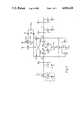
- FIG. 1shows the circuit diagram of sense amplifier according to this invention for a CMOS DRAM, together with DRAM components with which it is used such as a memory cell.
- FIG. 2shows the operation timing diagram of the circuit of FIG. 1.
- FIG. 1is the circuit diagram of the sense amplifier and memory cell according to this invention.
- Memory cellis composed of one NMOS transistor 10 and one storage capacitor 14 which are connected serially between a bit line (or row line) and a fixed voltage source (ground or power supply voltage Vcc).
- bit lineor row line
- Vccfixed voltage source
- several memory cellsare connected with polysilicon bit line BL and BL which are shorted with node points 37 and 38 of sense amplifier located at the center, respectively.
- polysilicon or metal word line WL 1 -WLn and WLo - WLware connected with the gates of pass transistors 10-13 of the above memory cells to activate the memory cell selectively according to row address.
- the sense amplifierhas a bistable flip-flop composed of cross-coupled NMOS transistors 20, 21 of which sources are connected in common with the drain of latch NMOS transistor 22.
- the source of NMOS transistor 22is grounded, and control pulse ⁇ 1 is applied on the gate.
- node points 35 and 36 of the above bistable flip-flopare connected with the polysilicon bit line BL and BL at node points 37 and 38 through pass NMOS transistors 23 and 24, respectively.
- Power supply voltage Vccis applied on the gates of above NMOS transistors 23 and 24.
- FIG. 1is the 1-transistor cells connected to one sense amplifier of the semiconductor CMOS DRAM system.
- NMOS transistor 25is shunted between nodes 37 and 36 for the equalization of bit line BL and BL.
- two pass transistors 26 and 27 connected seriallyare shunted between node points 37 and 38.
- Clock pulse ⁇ 5is applied on the gates of above equalization transistor 25 and two pass transistors 26 and 27.
- the connection junction of the pass transistors 26 and 27is connected with the reference voltage V REF . Therefore, when the above control pulse ⁇ 5 goes to the high state both of the bit lines BL and BL are charged with V REF voltage equally.
- a pair of PMOS transistors 28 and 29 of which drain and gate are cross-coupled to those of each otherare placed between above node points 37 and 38, and the drains of the both PMOS transistors are connected with node point 41 in common.
- the drain and source of the load PMOS transistor 30are connected with node point 41 and power supply voltage Vcc, respectively.
- the gate of the above PMOS transistor 30is connected with the drain of NMOS transistors 32 and source of NMOS transistor 31. These NMOS transistors are the useful means for the restore control of the above bit line.
- power supply voltage Vcc and control clock ⁇ 2are applied on the drain and gate of the above NMOS transistor 31. Also, the source and gate of the above NMOS transistor 32 are connected with ground and control clock ⁇ 3 , respectively.
- gated capacitors 33 and 34are connected with the above node points 39 and 41, respectively.
- Control clock ⁇ 4is applied on both of the above capacitors 33 and 34.
- the above clock ⁇ 4is applied before the word line goes to the low state.
- This clock voltageis propagated through the gated capacitors 33 and 34 to node points 39 and 41 to make PMOS transistor 30 go to OFF state.
- the voltage level of node point 41is stored along the bit line on the storage capacitor of memory cell selected by the addressed word line.
- FIG. 2shows the operation timing diagram of the circuit of FIG. 1 according to this invention. From now on, the operation mechanism of the circuit of FIG. 1 is explained with FIG. 2 in detail.
- row address signal xcomes from the well known row address decoder which is not drawn, after the row address strobe signal RAS goes to a low state in the conventional DRAM.
- the row selection address signal xprovides signal of Vcc+2V T voltage from the well known row address decoder.
- the reference voltage V REF applied on the node point 40may by equal to 1/2Vcc or Vcc-V T . From now on, it is assumed that V REF is equal to 1/2Vcc for the explanation.
- the reference voltage V REF applied on node point 40precharges the bit line BL and BL up to the V REF volt through the above NMOS pass transistors 26 and 27. Both of the bit lines BL and BL are made to be equal to V REF voltage level by the above NMOS transistor 25.
- Vcc+ ⁇ voltage levelis stored on the storage capacitor 14 of the memory cell 1 of FIG. 1.
- ⁇is a voltage larger than 2V T volt as will be explained.
- the NMOS pass transistor 10turns on so that there exists the voltage level difference between bit lines BL and BL due to the stored voltage on the above storage capacitor 14. This voltage difference propagates to nodes 35 and 36 through pass transistor 23 and 24, respectively, and is equal to about 50-2000 mV because the parasitic capacitance of bit line is far larger than the capacitance of the above storage capacitor 14.
- latch transistor 22turns on. Since the voltage level of the above node 35 is higher than that of node 36, NMOS transistor 21 turns on while the NMOS transistor 20 goes to OFF state. Consequently, the voltage of node 36 lowers to the ground level losing its charge through the above transistor 21 and 22, and large voltage difference between node 35 and 36 is developed.
- control clock ⁇ 2is changed from the high state (Vcc+2V T voltage level) to the low state (ground level)
- NMOS transistor 31turns off and as at time t 3 the control clock ⁇ 3 goes to the high state (Vcc level)
- node 39 at voltage level of Vccis connected to the ground by the conduction of NMOS transistor 32.
- bit line BLis restored to the power supply voltage level Vcc.
- control clock ⁇ 2goes to the high state (Vcc voltage level) and at the same time control clock ⁇ 3 goes to the low state (ground level) so that node point 39 is charged to Vcc-V T voltage level, and PMOS transistor 30 turns off.
- the PMOS transistor 30keeps its OFF state and Vcc+volt is stored on the storage capacitor 14 along the PMOS transistor 28, bit line BL and NMOS transistor 10 of the memory cell 1.
- the bit lines BL and BLare equalized to the reference voltage V REF .
- the voltage level of node 39is kept at Vcc level with control clock ⁇ 1 and ⁇ 4 in low state and control clock ⁇ 2 at Vcc+2V T level.
- voltage level larger than the power supply voltagecan be stored on one transistor memory cell so that soft error which comes from the leakage of the stored charge of storage capacitor due to the electron-hole generation by ⁇ -particle penetration can be avoided.
Landscapes
- Engineering & Computer Science (AREA)
- Microelectronics & Electronic Packaging (AREA)
- Computer Hardware Design (AREA)
- Power Engineering (AREA)
- Dram (AREA)
Abstract
Description
Claims (2)
Applications Claiming Priority (2)
| Application Number | Priority Date | Filing Date | Title |
|---|---|---|---|
| KR1019860009864AKR890004762B1 (en) | 1986-11-21 | 1986-11-21 | Sense Amplifiers for High Performance DRAM |
| KR86-9864 | 1986-11-21 |
Publications (1)
| Publication Number | Publication Date |
|---|---|
| US4855628Atrue US4855628A (en) | 1989-08-08 |
Family
ID=19253520
Family Applications (1)
| Application Number | Title | Priority Date | Filing Date |
|---|---|---|---|
| US07/120,985Expired - LifetimeUS4855628A (en) | 1986-11-21 | 1987-11-16 | Sense amplifier for high performance dram |
Country Status (3)
| Country | Link |
|---|---|
| US (1) | US4855628A (en) |
| JP (1) | JPS63288496A (en) |
| KR (1) | KR890004762B1 (en) |
Cited By (41)
| Publication number | Priority date | Publication date | Assignee | Title |
|---|---|---|---|---|
| US4979013A (en)* | 1986-03-13 | 1990-12-18 | Mitsubishi Denki Kabushiki Kaisha | Semiconductor memory device |
| US5130581A (en)* | 1989-11-28 | 1992-07-14 | Hyundai Electronics Industries Co., Ltd. | Sense amplifier in a dynamic RAM having double power lines |
| US5487051A (en)* | 1990-11-23 | 1996-01-23 | Network Computing Devices, Inc. | Image processor memory for expediting memory operations |
| US5506523A (en)* | 1994-03-01 | 1996-04-09 | Xilinx, Inc. | Sense circuit with selectable zero power single input function mode |
| US5525918A (en)* | 1994-12-27 | 1996-06-11 | Alliance Semiconductor Corporation | Pre-sense amplifier for monolithic memories |
| US5861767A (en)* | 1996-12-03 | 1999-01-19 | Cirrus Logic, Inc. | Digital step generators and circuits, systems and methods using the same |
| US5881005A (en)* | 1996-02-01 | 1999-03-09 | Hitachi, Ltd. | Semiconductor integrated circuit device having a constant delay-time circuit for different operating voltages |
| US5942918A (en)* | 1997-06-25 | 1999-08-24 | Sun Microsystems, Inc. | Method for resolving differential signals |
| US5942919A (en)* | 1997-06-25 | 1999-08-24 | Sun Microsystems, Inc. | Differential receiver including an enable circuit |
| US5955894A (en)* | 1997-06-25 | 1999-09-21 | Sun Microsystems, Inc. | Method for controlling the impedance of a driver circuit |
| US5982191A (en)* | 1997-06-25 | 1999-11-09 | Sun Microsystems, Inc. | Broadly distributed termination for buses using switched terminator logic |
| US5990701A (en)* | 1997-06-25 | 1999-11-23 | Sun Microsystems, Inc. | Method of broadly distributing termination for buses using switched terminators |
| US6060907A (en)* | 1997-06-25 | 2000-05-09 | Sun Microsystems, Inc. | Impedance control circuit |
| US6085033A (en)* | 1997-06-25 | 2000-07-04 | Sun Microsystems, Inc. | Method for determining bit element values for driver impedance control |
| US6105152A (en)* | 1993-04-13 | 2000-08-15 | Micron Technology, Inc. | Devices and methods for testing cell margin of memory devices |
| US6226207B1 (en)* | 1997-06-20 | 2001-05-01 | Hyundai Electronics Industries Co., Ltd. | Semiconductor device having an electric charge amplifier for amplifying bit line electric charge |
| EP0647029B1 (en)* | 1993-09-14 | 2001-07-04 | Intergraph Corporation | CMOS circuit for implementing Boolean functions |
| US6278306B1 (en) | 1999-06-07 | 2001-08-21 | Sun Microsystems, Inc. | Method for an output driver with improved slew rate control |
| US6281729B1 (en) | 1999-06-07 | 2001-08-28 | Sun Microsystems, Inc. | Output driver with improved slew rate control |
| US6281714B1 (en) | 1997-06-25 | 2001-08-28 | Sun Microsystems, Inc. | Differential receiver |
| US6294924B1 (en) | 1999-09-20 | 2001-09-25 | Sun Microsystems, Inc. | Dynamic termination logic driver with improved slew rate control |
| US6297677B1 (en) | 1999-09-20 | 2001-10-02 | Sun Microsystems, Inc. | Method for a dynamic termination logic driver with improved slew rate control |
| US6316957B1 (en) | 1999-09-20 | 2001-11-13 | Sun Microsystems, Inc. | Method for a dynamic termination logic driver with improved impedance control |
| US6339351B1 (en) | 1999-06-07 | 2002-01-15 | Sun Microsystems, Inc. | Output driver with improved impedance control |
| US6343036B1 (en)* | 1992-10-02 | 2002-01-29 | Samsung Electronics Co., Ltd. | Multi-bank dynamic random access memory devices having all bank precharge capability |
| US6366139B1 (en) | 1999-06-07 | 2002-04-02 | Sun Microsystems, Inc. | Method for an output driver with improved impedance control |
| US6411131B1 (en) | 1997-06-25 | 2002-06-25 | Sun Microsystems, Inc. | Method for differentiating a differential voltage signal using current based differentiation |
| US6420913B1 (en) | 1999-09-20 | 2002-07-16 | Sun Microsystems, Inc. | Dynamic termination logic driver with improved impedance control |
| US20020093074A1 (en)* | 1999-12-17 | 2002-07-18 | International Business Machines Corporation | Antifuses and methods for forming the same |
| US6438063B1 (en) | 1992-10-02 | 2002-08-20 | Samsung Electronics Co., Ltd. | Integrated circuit memory devices having selectable column addressing and methods of operating same |
| US6456120B1 (en)* | 2000-05-05 | 2002-09-24 | Industrial Technology Research Institute | Capacitor-coupling differential logic circuit |
| US6484293B1 (en) | 2000-07-14 | 2002-11-19 | Sun Microsystems, Inc. | Method for determining optimal configuration for multinode bus |
| US6496435B2 (en)* | 2001-01-05 | 2002-12-17 | Kabushiki Kaisha Toshiba | Sense amplifier control circuit of semiconductor memory device |
| US6639430B2 (en)* | 2001-02-27 | 2003-10-28 | Broadcom Corporation | High speed latch comparators |
| US20040136252A1 (en)* | 2003-01-13 | 2004-07-15 | Hirokazu Ueda | Method and apparatus for enhanced sensing of low voltage memory |
| US20050144419A1 (en)* | 2003-12-29 | 2005-06-30 | Sang-Hoon Hong | Semiconductor memory device having advanced tag block |
| US20060034113A1 (en)* | 2004-08-13 | 2006-02-16 | Micron Technology, Inc. | Capacitor supported precharging of memory digit lines |
| KR100621611B1 (en)* | 1999-05-10 | 2006-09-06 | 삼성전자주식회사 | High Voltage Generation Circuit of Semiconductor Device |
| US8462571B2 (en) | 2011-07-19 | 2013-06-11 | Elite Semiconductor Memory Technology Inc. | DRAM and method for testing the same in the wafer level burn-in test mode |
| TWI588838B (en)* | 2013-03-15 | 2017-06-21 | 萊迪思半導體公司 | Method and apparatus for implementing wide data range and wide common-mode receivers |
| US12217784B2 (en) | 2020-03-19 | 2025-02-04 | Rambus Inc. | Boosted writeback voltage |
Citations (3)
| Publication number | Priority date | Publication date | Assignee | Title |
|---|---|---|---|---|
| US4694205A (en)* | 1985-06-03 | 1987-09-15 | Advanced Micro Devices, Inc. | Midpoint sense amplification scheme for a CMOS DRAM |
| US4743784A (en)* | 1985-07-08 | 1988-05-10 | Nec Corporation | Sense amplifier circuit |
| US4748349A (en)* | 1978-09-22 | 1988-05-31 | Texas Instruments Incorporated | High performance dynamic sense amplifier with voltage boost for row address lines |
Family Cites Families (5)
| Publication number | Priority date | Publication date | Assignee | Title |
|---|---|---|---|---|
| JPS5352022A (en)* | 1976-10-22 | 1978-05-12 | Hitachi Ltd | Pre-amplifier |
| US4239991A (en)* | 1978-09-07 | 1980-12-16 | Texas Instruments Incorporated | Clock voltage generator for semiconductor memory |
| JPS5712484A (en)* | 1980-06-26 | 1982-01-22 | Mitsubishi Electric Corp | Differential amplifier |
| JPS58118135A (en)* | 1982-01-06 | 1983-07-14 | Hitachi Ltd | Semiconductor integrated circuit device |
| JPS60147997A (en)* | 1984-01-11 | 1985-08-05 | Toshiba Corp | Semiconductor storage device |
- 1986
- 1986-11-21KRKR1019860009864Apatent/KR890004762B1/ennot_activeExpired
- 1987
- 1987-11-16USUS07/120,985patent/US4855628A/ennot_activeExpired - Lifetime
- 1987-11-20JPJP62292211Apatent/JPS63288496A/enactiveGranted
Patent Citations (3)
| Publication number | Priority date | Publication date | Assignee | Title |
|---|---|---|---|---|
| US4748349A (en)* | 1978-09-22 | 1988-05-31 | Texas Instruments Incorporated | High performance dynamic sense amplifier with voltage boost for row address lines |
| US4694205A (en)* | 1985-06-03 | 1987-09-15 | Advanced Micro Devices, Inc. | Midpoint sense amplification scheme for a CMOS DRAM |
| US4743784A (en)* | 1985-07-08 | 1988-05-10 | Nec Corporation | Sense amplifier circuit |
Cited By (62)
| Publication number | Priority date | Publication date | Assignee | Title |
|---|---|---|---|---|
| US4979013A (en)* | 1986-03-13 | 1990-12-18 | Mitsubishi Denki Kabushiki Kaisha | Semiconductor memory device |
| US5130581A (en)* | 1989-11-28 | 1992-07-14 | Hyundai Electronics Industries Co., Ltd. | Sense amplifier in a dynamic RAM having double power lines |
| US5487051A (en)* | 1990-11-23 | 1996-01-23 | Network Computing Devices, Inc. | Image processor memory for expediting memory operations |
| US6438063B1 (en) | 1992-10-02 | 2002-08-20 | Samsung Electronics Co., Ltd. | Integrated circuit memory devices having selectable column addressing and methods of operating same |
| US6343036B1 (en)* | 1992-10-02 | 2002-01-29 | Samsung Electronics Co., Ltd. | Multi-bank dynamic random access memory devices having all bank precharge capability |
| US6105152A (en)* | 1993-04-13 | 2000-08-15 | Micron Technology, Inc. | Devices and methods for testing cell margin of memory devices |
| US6230292B1 (en) | 1993-04-13 | 2001-05-08 | Micron Technology, Inc. | Devices and method for testing cell margin of memory devices |
| EP0647029B1 (en)* | 1993-09-14 | 2001-07-04 | Intergraph Corporation | CMOS circuit for implementing Boolean functions |
| US5506523A (en)* | 1994-03-01 | 1996-04-09 | Xilinx, Inc. | Sense circuit with selectable zero power single input function mode |
| US5525918A (en)* | 1994-12-27 | 1996-06-11 | Alliance Semiconductor Corporation | Pre-sense amplifier for monolithic memories |
| US5881005A (en)* | 1996-02-01 | 1999-03-09 | Hitachi, Ltd. | Semiconductor integrated circuit device having a constant delay-time circuit for different operating voltages |
| US5861767A (en)* | 1996-12-03 | 1999-01-19 | Cirrus Logic, Inc. | Digital step generators and circuits, systems and methods using the same |
| US6226207B1 (en)* | 1997-06-20 | 2001-05-01 | Hyundai Electronics Industries Co., Ltd. | Semiconductor device having an electric charge amplifier for amplifying bit line electric charge |
| US5942918A (en)* | 1997-06-25 | 1999-08-24 | Sun Microsystems, Inc. | Method for resolving differential signals |
| US5955894A (en)* | 1997-06-25 | 1999-09-21 | Sun Microsystems, Inc. | Method for controlling the impedance of a driver circuit |
| US6147515A (en)* | 1997-06-25 | 2000-11-14 | Sun Microsystems, Inc. | Differential receiver |
| US6060907A (en)* | 1997-06-25 | 2000-05-09 | Sun Microsystems, Inc. | Impedance control circuit |
| US5990701A (en)* | 1997-06-25 | 1999-11-23 | Sun Microsystems, Inc. | Method of broadly distributing termination for buses using switched terminators |
| US5982191A (en)* | 1997-06-25 | 1999-11-09 | Sun Microsystems, Inc. | Broadly distributed termination for buses using switched terminator logic |
| US6411131B1 (en) | 1997-06-25 | 2002-06-25 | Sun Microsystems, Inc. | Method for differentiating a differential voltage signal using current based differentiation |
| US5942919A (en)* | 1997-06-25 | 1999-08-24 | Sun Microsystems, Inc. | Differential receiver including an enable circuit |
| US6281714B1 (en) | 1997-06-25 | 2001-08-28 | Sun Microsystems, Inc. | Differential receiver |
| US6085033A (en)* | 1997-06-25 | 2000-07-04 | Sun Microsystems, Inc. | Method for determining bit element values for driver impedance control |
| KR100621611B1 (en)* | 1999-05-10 | 2006-09-06 | 삼성전자주식회사 | High Voltage Generation Circuit of Semiconductor Device |
| US6281729B1 (en) | 1999-06-07 | 2001-08-28 | Sun Microsystems, Inc. | Output driver with improved slew rate control |
| US6339351B1 (en) | 1999-06-07 | 2002-01-15 | Sun Microsystems, Inc. | Output driver with improved impedance control |
| US6278306B1 (en) | 1999-06-07 | 2001-08-21 | Sun Microsystems, Inc. | Method for an output driver with improved slew rate control |
| US6366139B1 (en) | 1999-06-07 | 2002-04-02 | Sun Microsystems, Inc. | Method for an output driver with improved impedance control |
| US6420913B1 (en) | 1999-09-20 | 2002-07-16 | Sun Microsystems, Inc. | Dynamic termination logic driver with improved impedance control |
| US6316957B1 (en) | 1999-09-20 | 2001-11-13 | Sun Microsystems, Inc. | Method for a dynamic termination logic driver with improved impedance control |
| US6297677B1 (en) | 1999-09-20 | 2001-10-02 | Sun Microsystems, Inc. | Method for a dynamic termination logic driver with improved slew rate control |
| US6294924B1 (en) | 1999-09-20 | 2001-09-25 | Sun Microsystems, Inc. | Dynamic termination logic driver with improved slew rate control |
| US6608506B2 (en) | 1999-09-20 | 2003-08-19 | Sun Microsystems, Inc. | Dynamic termination logic driver with improved impedance control |
| US20020093074A1 (en)* | 1999-12-17 | 2002-07-18 | International Business Machines Corporation | Antifuses and methods for forming the same |
| US6812122B2 (en)* | 1999-12-17 | 2004-11-02 | International Business Machines Corporation | Method for forming a voltage programming element |
| US6456120B1 (en)* | 2000-05-05 | 2002-09-24 | Industrial Technology Research Institute | Capacitor-coupling differential logic circuit |
| US6484293B1 (en) | 2000-07-14 | 2002-11-19 | Sun Microsystems, Inc. | Method for determining optimal configuration for multinode bus |
| US6674678B2 (en) | 2001-01-05 | 2004-01-06 | Kabushiki Kaisha Toshiba | Sense amplifier control circuit of semiconductor memory device |
| US6496435B2 (en)* | 2001-01-05 | 2002-12-17 | Kabushiki Kaisha Toshiba | Sense amplifier control circuit of semiconductor memory device |
| US20080143391A1 (en)* | 2001-02-27 | 2008-06-19 | Broadcom Corporation | High Speed Latch Comparators |
| US6639430B2 (en)* | 2001-02-27 | 2003-10-28 | Broadcom Corporation | High speed latch comparators |
| US8410820B2 (en) | 2001-02-27 | 2013-04-02 | Broadcom Corporation | High speed latch comparators |
| US20110133967A1 (en)* | 2001-02-27 | 2011-06-09 | Broadcom Corporation | High Speed Latch Comparators |
| US20040041611A1 (en)* | 2001-02-27 | 2004-03-04 | Broadcom Corporation | High speed latch comparators |
| US7906992B2 (en) | 2001-02-27 | 2011-03-15 | Broadcom Corporation | High speed latch comparators |
| US7352215B2 (en) | 2001-02-27 | 2008-04-01 | Broadcom Corporation | High speed latch comparators |
| US20040136252A1 (en)* | 2003-01-13 | 2004-07-15 | Hirokazu Ueda | Method and apparatus for enhanced sensing of low voltage memory |
| US6873559B2 (en) | 2003-01-13 | 2005-03-29 | Micron Technology, Inc. | Method and apparatus for enhanced sensing of low voltage memory |
| US20050122792A1 (en)* | 2003-01-13 | 2005-06-09 | Hirokazu Ueda | Method and apparatus for enhanced sensing of low voltage memory |
| US7116596B2 (en) | 2003-01-13 | 2006-10-03 | Micron Technology, Inc. | Method of apparatus for enhanced sensing of low voltage memory |
| US20110085405A1 (en)* | 2003-12-29 | 2011-04-14 | Sang-Hoon Hong | Semiconductor memory device having advanced tag block |
| US7870362B2 (en)* | 2003-12-29 | 2011-01-11 | Hynix Semiconductor Inc. | Semiconductor memory device having advanced tag block |
| US20050144419A1 (en)* | 2003-12-29 | 2005-06-30 | Sang-Hoon Hong | Semiconductor memory device having advanced tag block |
| US7423923B2 (en) | 2004-08-13 | 2008-09-09 | Micron Technology, Inc. | Capacitor supported precharging of memory digit lines |
| US20090003038A1 (en)* | 2004-08-13 | 2009-01-01 | Micron Technology, Inc. | Capacitor supported precharching of memory digit lines |
| US7663952B2 (en) | 2004-08-13 | 2010-02-16 | Micron Technology, Inc. | Capacitor supported precharging of memory digit lines |
| US20070097764A1 (en)* | 2004-08-13 | 2007-05-03 | Shigeki Tomishima | Capacitor supported precharging of memory digit lines |
| US7177213B2 (en) | 2004-08-13 | 2007-02-13 | Micron Technology, Inc. | Capacitor supported precharging of memory digit lines |
| US20060034113A1 (en)* | 2004-08-13 | 2006-02-16 | Micron Technology, Inc. | Capacitor supported precharging of memory digit lines |
| US8462571B2 (en) | 2011-07-19 | 2013-06-11 | Elite Semiconductor Memory Technology Inc. | DRAM and method for testing the same in the wafer level burn-in test mode |
| TWI588838B (en)* | 2013-03-15 | 2017-06-21 | 萊迪思半導體公司 | Method and apparatus for implementing wide data range and wide common-mode receivers |
| US12217784B2 (en) | 2020-03-19 | 2025-02-04 | Rambus Inc. | Boosted writeback voltage |
Also Published As
| Publication number | Publication date |
|---|---|
| JPS63288496A (en) | 1988-11-25 |
| KR880006837A (en) | 1988-07-25 |
| KR890004762B1 (en) | 1989-11-25 |
| JPH0462436B2 (en) | 1992-10-06 |
Similar Documents
| Publication | Publication Date | Title |
|---|---|---|
| US4855628A (en) | Sense amplifier for high performance dram | |
| US4584672A (en) | CMOS dynamic random-access memory with active cycle one half power supply potential bit line precharge | |
| EP0867026B1 (en) | Low voltage dynamic memory | |
| US5812476A (en) | Refresh circuit for DRAM with three-transistor type memory cells | |
| US5339274A (en) | Variable bitline precharge voltage sensing technique for DRAM structures | |
| JPH10334656A (en) | Multi-transistor dynamic random access memory array architecture for simultaneous refresh of multiple memory cells during a read operation | |
| US5255235A (en) | Dynamic random access memory with dummy word lines connected to bit line potential adjusting capacitors | |
| US4397003A (en) | Dynamic random access memory | |
| US5808955A (en) | Integrated circuit memory devices including sub-word line drivers and related methods | |
| US5684749A (en) | Single-ended sensing using global bit lines for dram | |
| US4980862A (en) | Folded bitline dynamic ram with reduced shared supply voltages | |
| US4982367A (en) | Dynamic random access memory with well-balanced read-out voltage on bit line pair and operating method therefor | |
| US5280452A (en) | Power saving semsing circuits for dynamic random access memory | |
| US20040037138A1 (en) | Direct read of dram cell using high transfer ratio | |
| US4477886A (en) | Sense/restore circuit for dynamic random access memory | |
| US6292417B1 (en) | Memory device with reduced bit line pre-charge voltage | |
| US5438543A (en) | Semiconductor memory using low power supply voltage | |
| US4409672A (en) | Dynamic semiconductor memory device | |
| US6570799B1 (en) | Precharge and reference voltage technique for dynamic random access memories | |
| US5745423A (en) | Low power precharge circuit for a dynamic random access memory | |
| WO1991001557A2 (en) | Dynamic random access memory with improved sensing and refreshing | |
| US5333128A (en) | Semiconductor memory device having a circuit for reducing frequency of proceeding refresh in data retention mode | |
| US5894444A (en) | Cell plate referencing for dram sensing | |
| US5777934A (en) | Semiconductor memory device with variable plate voltage generator | |
| US6111803A (en) | Reduced cell voltage for memory device |
Legal Events
| Date | Code | Title | Description |
|---|---|---|---|
| AS | Assignment | Owner name:SAMSUNG SEMICONDUCTOR AND TELECOMMUNICATIONS CO., Free format text:ASSIGNMENT OF ASSIGNORS INTEREST.;ASSIGNOR:JUN, DONG-SOO;REEL/FRAME:004821/0003 Effective date:19871221 Owner name:SAMSUNG SEMICONDUCTOR AND TELECOMMUNICATIONS CO., Free format text:ASSIGNMENT OF ASSIGNORS INTEREST;ASSIGNOR:JUN, DONG-SOO;REEL/FRAME:004821/0003 Effective date:19871221 | |
| STCF | Information on status: patent grant | Free format text:PATENTED CASE | |
| FEPP | Fee payment procedure | Free format text:PAYOR NUMBER ASSIGNED (ORIGINAL EVENT CODE: ASPN); ENTITY STATUS OF PATENT OWNER: LARGE ENTITY | |
| FPAY | Fee payment | Year of fee payment:4 | |
| FPAY | Fee payment | Year of fee payment:8 | |
| FEPP | Fee payment procedure | Free format text:PAYER NUMBER DE-ASSIGNED (ORIGINAL EVENT CODE: RMPN); ENTITY STATUS OF PATENT OWNER: LARGE ENTITY Free format text:PAYOR NUMBER ASSIGNED (ORIGINAL EVENT CODE: ASPN); ENTITY STATUS OF PATENT OWNER: LARGE ENTITY | |
| FPAY | Fee payment | Year of fee payment:12 |