US4855247A - Process for fabricating self-aligned silicide lightly doped drain MOS devices - Google Patents
Process for fabricating self-aligned silicide lightly doped drain MOS devicesDownload PDFInfo
- Publication number
- US4855247A US4855247AUS07/291,541US29154188AUS4855247AUS 4855247 AUS4855247 AUS 4855247AUS 29154188 AUS29154188 AUS 29154188AUS 4855247 AUS4855247 AUS 4855247A
- Authority
- US
- United States
- Prior art keywords
- layer
- side wall
- wall spacer
- silicon dioxide
- etch
- Prior art date
- Legal status (The legal status is an assumption and is not a legal conclusion. Google has not performed a legal analysis and makes no representation as to the accuracy of the status listed.)
- Expired - Lifetime
Links
Images

Classifications
- H—ELECTRICITY
- H01—ELECTRIC ELEMENTS
- H01L—SEMICONDUCTOR DEVICES NOT COVERED BY CLASS H10
- H01L21/00—Processes or apparatus adapted for the manufacture or treatment of semiconductor or solid state devices or of parts thereof
- H01L21/02—Manufacture or treatment of semiconductor devices or of parts thereof
- H01L21/04—Manufacture or treatment of semiconductor devices or of parts thereof the devices having potential barriers, e.g. a PN junction, depletion layer or carrier concentration layer
- H01L21/18—Manufacture or treatment of semiconductor devices or of parts thereof the devices having potential barriers, e.g. a PN junction, depletion layer or carrier concentration layer the devices having semiconductor bodies comprising elements of Group IV of the Periodic Table or AIIIBV compounds with or without impurities, e.g. doping materials
- H01L21/28—Manufacture of electrodes on semiconductor bodies using processes or apparatus not provided for in groups H01L21/20 - H01L21/268
- H01L21/283—Deposition of conductive or insulating materials for electrodes conducting electric current
- H01L21/285—Deposition of conductive or insulating materials for electrodes conducting electric current from a gas or vapour, e.g. condensation
- H01L21/28506—Deposition of conductive or insulating materials for electrodes conducting electric current from a gas or vapour, e.g. condensation of conductive layers
- H01L21/28512—Deposition of conductive or insulating materials for electrodes conducting electric current from a gas or vapour, e.g. condensation of conductive layers on semiconductor bodies comprising elements of Group IV of the Periodic Table
- H01L21/28518—Deposition of conductive or insulating materials for electrodes conducting electric current from a gas or vapour, e.g. condensation of conductive layers on semiconductor bodies comprising elements of Group IV of the Periodic Table the conductive layers comprising silicides
- H—ELECTRICITY
- H01—ELECTRIC ELEMENTS
- H01L—SEMICONDUCTOR DEVICES NOT COVERED BY CLASS H10
- H01L21/00—Processes or apparatus adapted for the manufacture or treatment of semiconductor or solid state devices or of parts thereof
- H01L21/02—Manufacture or treatment of semiconductor devices or of parts thereof
- H01L21/027—Making masks on semiconductor bodies for further photolithographic processing not provided for in group H01L21/18 or H01L21/34
- H01L21/033—Making masks on semiconductor bodies for further photolithographic processing not provided for in group H01L21/18 or H01L21/34 comprising inorganic layers
- H01L21/0334—Making masks on semiconductor bodies for further photolithographic processing not provided for in group H01L21/18 or H01L21/34 comprising inorganic layers characterised by their size, orientation, disposition, behaviour, shape, in horizontal or vertical plane
- H01L21/0337—Making masks on semiconductor bodies for further photolithographic processing not provided for in group H01L21/18 or H01L21/34 comprising inorganic layers characterised by their size, orientation, disposition, behaviour, shape, in horizontal or vertical plane characterised by the process involved to create the mask, e.g. lift-off masks, sidewalls, or to modify the mask, e.g. pre-treatment, post-treatment
- H—ELECTRICITY
- H10—SEMICONDUCTOR DEVICES; ELECTRIC SOLID-STATE DEVICES NOT OTHERWISE PROVIDED FOR
- H10D—INORGANIC ELECTRIC SEMICONDUCTOR DEVICES
- H10D30/00—Field-effect transistors [FET]
- H10D30/01—Manufacture or treatment
- H10D30/021—Manufacture or treatment of FETs having insulated gates [IGFET]
- H10D30/0223—Manufacture or treatment of FETs having insulated gates [IGFET] having source and drain regions or source and drain extensions self-aligned to sides of the gate
- H10D30/0227—Manufacture or treatment of FETs having insulated gates [IGFET] having source and drain regions or source and drain extensions self-aligned to sides of the gate having both lightly-doped source and drain extensions and source and drain regions self-aligned to the sides of the gate, e.g. lightly-doped drain [LDD] MOSFET or double-diffused drain [DDD] MOSFET
- H10D30/0229—Manufacture or treatment of FETs having insulated gates [IGFET] having source and drain regions or source and drain extensions self-aligned to sides of the gate having both lightly-doped source and drain extensions and source and drain regions self-aligned to the sides of the gate, e.g. lightly-doped drain [LDD] MOSFET or double-diffused drain [DDD] MOSFET forming drain regions and lightly-doped drain [LDD] simultaneously, e.g. using implantation through a T-shaped mask
- H—ELECTRICITY
- H10—SEMICONDUCTOR DEVICES; ELECTRIC SOLID-STATE DEVICES NOT OTHERWISE PROVIDED FOR
- H10D—INORGANIC ELECTRIC SEMICONDUCTOR DEVICES
- H10D64/00—Electrodes of devices having potential barriers
- H10D64/01—Manufacture or treatment
- H10D64/021—Manufacture or treatment using multiple gate spacer layers, e.g. bilayered sidewall spacers
- H—ELECTRICITY
- H10—SEMICONDUCTOR DEVICES; ELECTRIC SOLID-STATE DEVICES NOT OTHERWISE PROVIDED FOR
- H10D—INORGANIC ELECTRIC SEMICONDUCTOR DEVICES
- H10D30/00—Field-effect transistors [FET]
- H10D30/01—Manufacture or treatment
- H10D30/021—Manufacture or treatment of FETs having insulated gates [IGFET]
- H10D30/0212—Manufacture or treatment of FETs having insulated gates [IGFET] using self-aligned silicidation
- Y—GENERAL TAGGING OF NEW TECHNOLOGICAL DEVELOPMENTS; GENERAL TAGGING OF CROSS-SECTIONAL TECHNOLOGIES SPANNING OVER SEVERAL SECTIONS OF THE IPC; TECHNICAL SUBJECTS COVERED BY FORMER USPC CROSS-REFERENCE ART COLLECTIONS [XRACs] AND DIGESTS
- Y10—TECHNICAL SUBJECTS COVERED BY FORMER USPC
- Y10S—TECHNICAL SUBJECTS COVERED BY FORMER USPC CROSS-REFERENCE ART COLLECTIONS [XRACs] AND DIGESTS
- Y10S148/00—Metal treatment
- Y10S148/105—Masks, metal
- Y—GENERAL TAGGING OF NEW TECHNOLOGICAL DEVELOPMENTS; GENERAL TAGGING OF CROSS-SECTIONAL TECHNOLOGIES SPANNING OVER SEVERAL SECTIONS OF THE IPC; TECHNICAL SUBJECTS COVERED BY FORMER USPC CROSS-REFERENCE ART COLLECTIONS [XRACs] AND DIGESTS
- Y10—TECHNICAL SUBJECTS COVERED BY FORMER USPC
- Y10S—TECHNICAL SUBJECTS COVERED BY FORMER USPC CROSS-REFERENCE ART COLLECTIONS [XRACs] AND DIGESTS
- Y10S148/00—Metal treatment
- Y10S148/147—Silicides
- Y—GENERAL TAGGING OF NEW TECHNOLOGICAL DEVELOPMENTS; GENERAL TAGGING OF CROSS-SECTIONAL TECHNOLOGIES SPANNING OVER SEVERAL SECTIONS OF THE IPC; TECHNICAL SUBJECTS COVERED BY FORMER USPC CROSS-REFERENCE ART COLLECTIONS [XRACs] AND DIGESTS
- Y10—TECHNICAL SUBJECTS COVERED BY FORMER USPC
- Y10S—TECHNICAL SUBJECTS COVERED BY FORMER USPC CROSS-REFERENCE ART COLLECTIONS [XRACs] AND DIGESTS
- Y10S257/00—Active solid-state devices, e.g. transistors, solid-state diodes
- Y10S257/90—MOSFET type gate sidewall insulating spacer
Definitions
- This inventionrelates generally to the fabrication of metal-silicon dioxide semiconductor (MOS) devices, and more particularly to the fabrication of self-aligned silicide and lightly doped drain MOS device structures.
- MOSmetal-silicon dioxide semiconductor
- MOS devicesin which ever-decreasing device dimensions are realized in order to achieve greater device density and increased operating speeds. This decrease in MOS device dimensions has, however, created a concern over the high sheet resistance in the source/drain regions and hot carrier injection.
- junction depths of the source/drain regionsare reduced so as to minimize parasitic effects.
- One direct result of this reduction in the source/drain junction depthis an increase of the sheet resistance of the source/drain regions.
- Another result of decreasing device dimensionsbears on the junction integrity when a metal layer is applied to make a contact to the source/drain regions. The shallower the junction, the more difficult it is to reduce the leakage current of the source/drain regions to the substrate.
- a device structureIn order to reduce the sheet resistance of the source/drain regions, a device structure has been developed, known as a self-aligned silicide structure, in which a metal silicide film is formed at the source/drain regions as well as at the polysilicon gate.
- a silicon dioxide side wall spaceris formed before the source/drain and polysilicon regions are silicided.
- the side wall spacer etchhas to clear the source/drain regions that are not intended to be covered by the side wall spacer so that these regions can be silicided.
- any significant etch into the silicon of the source/drain regionswill reduce the junction depth.
- MOS integrated circuitsare also enhanced by decreasing the separation between the source and drain of an MOS transistor, also known as the effective channel length.
- the applied drain-to-source voltageis kept at a constant level irrespective of reductions in channel length which results in a higher electric field being established across the channel region.
- This elevated electric fieldhas the ability to inject the carriers (electrons or holes) in the channel region across the silicon and silicon dioxide interface and to trap the carriers in the oxide. Since the silicon dioxide layer forms the gate insulator of the MOS device, the trapped charges in the gate oxide have an effect on the electrical characteristics of the device. This is a particular concern from the reliability standpoint since the longer the drain-to-source voltage is applied, the more charges are trapped.
- LDDlightly doped drain
- SWS-LDDside wall spacer lightly doped drain
- the construction of the SWS-LDD devicerequires the formation of a side wall spacer that is adjacent to the polysilicon gate. This side wall spacer is formed between two ion implantation steps; the first is a light implant, the second is a heavy implant to define the lightly and heavily doped regions, respectively.
- CMOScomplementary MOS
- two lithographic stepsare required for each dopant polarity, one for each of the implants.
- only one such lithographic stepis required since only one implant is needed.
- the junctionsbe formed after silicidation, so that the impurities are implanted into or through the silicide. During the subsequent heat treatment, impurities in the silicide diffuse into the silicon to form the junctions.
- a self-aligned silicideis implemented with an SWS-LDD structure on a CMOS device, one additional lithographic step is required for each dopant polarity to fabricate the device.
- the side wall spacer etchinghas to be critically controlled
- SWS-LDDlightly doped drain
- a layer of materialis grown or deposited before the deposition of the side wall spacer material.
- the material of this layerhas a different etching characteristic than that of the side wall spacer material and the silicon substrate. During the subsequent side wall spacer etch, this material serves as an etching stop.
- a second and different etch that has a substantially lower etch rate of the silicon substrate and side wall spacer materialis then applied to remove the material in areas not covered by the side wall spacer.
- a polysilicon gateis defined and a first layer is grown before the deposition of the side wall spacer material.
- the material of the first layerhas a different etching characteristic than that of the silicon substrate and side wall spacer material. During the subsequent side wall spacer etch, this material serves as an etching stop.
- a second and different etch that has a substantially lower etch rate of the silicon substrate and side wall spacer materialis then applied to remove the first layer of material in areas not covered by the side wall spacer.
- a second layer of materialis grown over the exposed silicon substrate to a thickness whose ion implantation stopping power is less than that of the first layer.
- the side wall spaceris then removed, and two sequential ion implantations of the same polarity are performed after a lithographic step to define the regions that are to receive such implants. These two implants define, respectively, the lightly and heavily doped regions.
- a first layer of materialis deposited before the deposition of the side wall spacer material.
- This first layer of materialhas a different etching characteristic than that of the silicon substrate and side wall spacer material. During the subsequent side wall spacer etch, this material serves as an etching stop.
- a second and different etch that has a substantially lower etch rate of the silicon substrate and side wall spacer materialis applied to remove this material in the area not covered by the side wall spacer. Silicide is formed selectively over the silicon and polysilicon regions and the side wall spacer is etched away.
- a layer of a second materialmay be selectively grown or deposited over the silicide but not on the side wall spacer.
- this second materialhas a different etching characteristic than that of the side wall spacer material. During the etching to remove the side wall spacer, this second material serves as an etching stop to protect the formed silicide layer.
- a lithographic stepis performed to define the proper regions, and two sequential ion implants of the same dopant polarity are applied to form the lightly and heavily doped regions, respectively.
- the present inventionrelates to an improved process for fabricating MOS devices substantially as defined in the appended claims and as described in the following specification as considered with the accompanying drawings in which:
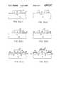
- FIGS. 1(a)-1(e)are cross sections of a self-aligned silicide MOS device at various stages in its fabrication in accordance with a first embodiment of the invention
- FIGS. 2(a)-2(c)are cross sections of an SWS-LDD MOS device at various stages of its fabrication in accordance with a second embodiment of the invention.
- FIGS. 3(a)-3(c)are cross sections of a self-aligned silicide LDD MOS device at various stages of its fabrication in accordance with a third embodiment of the invention.
- FIG. 1(a)a self-aligned silicide MOS integrated circuit in an early stage of its fabrication in accordance with one embodiment of the invention.
- a silicon dioxide film 12is grown over the upper surface of a silicon substrate 10.
- a polysilicon gate 14is defined over the film 12 and source/drain regions 16 are formed in the substrate 10 such as by diffusion or ion implantation.
- the silicon dioxide film 12 sandwiched between the substrate 10 and polysilicon gate 14is to serve, in a known manner, as the gate insulation of the completed MOS device.
- a layer of silicon dioxide 20is then grown over the exposed surface of the substrate 10 and over the polysilicon gate 14.
- the silicon dioxide layer 20may be either thermally grown or deposited by a chemical vapor deposition (CVD) method.
- the thickness of the silicon dioxide layer 20is such that it does not consume too much polysilicon and the silicon substrate if it is thermally grown, but thick enough to be a good etch stop for the subsequent side wall spacer etch. If the silicon dioxide layer 20 is deposited by a CVD method, there is no concern for polysilicon and silicon consumption. A thickness of the silicon dioxide layer 20 between 150 A and 2000 A is sufficient for this purpose.
- a layer of silicon nitride 23is subsequently deposited by a CVD method, which later in the process forms the side wall spacer.
- the thickness of the silicon nitride layer 23is determined by the desired width of the side wall spacer, which also depends on other factors such as the angle of the polysilicon side wall profile and the thickness of polysilicon. A thickness of silicon nitride layer 23 of 1000A or greater is needed for practical applications.
- a directional silicon nitride etchis performed to form the silicon nitride side wall spacer 24. This is done preferably in a plasma etcher or in a reactive ion etcher.
- the etching processshould have a sufficiently high silicon nitride etch rate and a sufficiently low oxide etch rate (good silicon nitride-to-silicon dioxide selectivity). The etch should stop when the silicon nitride in the planar surface is completely removed.
- the first stephas the following conditions: pressure: 325 mtorr; power: 175 watt; with a gas flow of 10 sccm of argon and 60 sccm of sulfur hexafluoride (SF 6 )
- the second stepconsists of: pressure: 325 mtorr; power: 100 watt; gas flow: 6 sccm of argon, 30 sccm of SF 6 and 5 sccm of chlorodifluoromethane (CHClF 2 )
- a silicon dioxide etchis then performed.
- This etchshould have a very high silicon dioxide-to-silicon and silicon dioxide-to-silicon nitride selectivity such as can be achieved by the use of wet buffered hydrofluoric acid.
- the etchas shown in FIG. 1(c), completely removes the silicon dioxide 20 over the polysilicon gate 14 as well as over the source/drain regions 16 that are not covered by the silicon nitride side wall spacer 24. As shown in FIG. 1(c), a portion 22 of the silicon dioxide layer covered by the silicon nitride side wall spacer (24) remains after the etch.
- an additional silicon dioxide layer 20is grown and a silicon nitride rather than a silicon dioxide side wall spacer is used.
- a silicon nitriderather than a silicon dioxide side wall spacer.
- the side wall spacer etchin the conventional process, one has to optimize the silicon dioxide-to-silicon etch selectivity and uniformity as well as the deposited silicon dioxide uniformity.
- the additional silicon dioxide layerbeing a material of different etching characteristics than the silicon and the silicon nitride that forms the side wall spacer, selectivity and uniformity can be independently controlled.
- silicon nitride-to-silicon dioxide etch selectivityshould be maintained, which is a commonly known technique in silicon device fabrication, there is greater latitude in the silicon nitride side wall spacer etching process, since one has only to concentrate mainly on the uniformity of the etch. As long as sufficient silicon dioxide is grown in the first place, the silicon nitride-to-silicon dioxide selectivity is not as important since the silicon dioxide layer eventually is removed. This is true, in particular, since this subsequent silicon dioxide etch can be made to have very high silicon dioxide-to-silicon selectivity by the application of such chemicals as buffered hydrofluoric acid.
- the amount of top layer of silicon removed in the source/drain junction areais determined by the thermally grown silicon dioxide layer 20, which can be very accurately controlled.
- the growing of the silicon oxidehas the additional benefit of driving in the source/drain junction. If the silicon dioxide layer 20 is deposited by a CVD method, no such silicon loss is encountered.
- the silicon layer removed in the conventional processis determined by the side wall spacer etch which has to be compromised with respect to the uniformity of the silicon dioxide deposited and the uniformity of the side wall spacer etch. As a result, it is not as easily controlled.
- the method of the invention illustrated in FIG. 2may be used to fabricate a CMOS SWS-LDD structure with one lithographic step for each source/drain dopant polarity.
- the objective in this methodis to create two different layer thicknesses over the source/drain regions before they receive the implants.
- the process sequenceis identical to the first method illustrated in FIG. 1 up to the side wall spacer formation except that in the method of FIG. 2, the source/drain dopants are not introduced before the side wall spacer formation.
- FIG. 2(a)The MOS device in an early stage of its fabrication in accordance with the method of FIG. 2 is illustrated in FIG. 2(a) As therein shown, a layer of insulating material 12, such as silicon dioxide, is formed on a silicon substrate 10 and separates the substrate 10 and a polysilicon gate 14. The silicon dioxide layer 20 and the silicon nitride side wall spacer 24 are formed as in the first method.
- insulating material 12such as silicon dioxide
- a silicon dioxide etch that has a high selectivity over silicon nitrideis then performed, preferably with a plasma etching or reactive ion etching technique because of their superior etch rate control.
- the etchremoves part of the silicon dioxide that is not protected by the silicon nitride to leave a silicon dioxide layer 28 having a reduced thickness between 100 A and 1800 A, as shown in FIG. 2(b).
- the silicon dioxide that is not covered by the silicon nitridecan be completely removed by a wet chemical such as a buffered hydrofluoric acid etching technique.
- a thin layer of silicon dioxidemay be regrown to a thickness between 100 A and 1800 A to produce the same structure as in FIG. 2(b).
- the first layer of material deposited before the side wall spacer deposition and the regrown layerneed not be the same material.
- the thickness of the silicon dioxide 28 not covered by the silicon nitride side wall spacercan be more precisely controlled.
- another layer of silicon dioxide 30is formed on top of polysilicon gate 14.
- two different thicknesses of silicon dioxideare present over the source/drain regions that are to be formed.
- One silicon dioxide layeris under the silicon nitride side wall spacer 24 whose thickness is the same as silicon dioxide layer 20 in FIG. 2(a) and is determined by the initial growth/deposition conditions.
- the other silicon dioxide layer 28is not covered by the silicon nitride side wall spacer. Silicon dioxide layer 28 should be thinner than layer 22 and its thickness is controlled by either the etching process or the regrowth process described above.
- the waferis then subjected to a silicon nitride etch that completely removes the silicon nitride side wall spacer. This can be accomplished in hot phosphoric acid etch or a plasma etch.
- a lithographic stepis performed (not shown in the figure) to define the proper regions to receive the subsequent implants, and two separate, sequential source/drain ion implants are then performed. After a thermal anneal of the implant, the device structure is in the form shown in FIG. 2(c).
- One of the ion implantsis a light implant to dope both the lightly doped region 32 and heavily doped region 34.
- the other ion implantis a heavy implant to define primarily the heavily doped region 34.
- the implant conditionsare optimized to utilize the different silicon dioxide thicknesses over the source/drain regions. This selection can be accomplished by using two different species of the same polarity (such as arsenic and phosphorus for the n-type dopant) that have significantly different penetration depths (projected ranges). It can also be accomplished by using the same species but with different implant energies resulting in different penetration depths.
- the actual implant conditionsare subject to other considerations such as the desired sheet resistance of each of the doped regions, and the surface concentration of the lightly doped region, which also determines the hot carrier injection immunity of the structure.
- the ion implant conditionis also influenced by the subsequent thermal anneal to allow sufficient lateral movement of the lightly doped region to cross the width of the silicon dioxide 18 on the polysilicon side wall. This latter consideration also plays a role in determining the initial thickness of the silicon dioxide layer 20.
- FIG. 3illustrates a process in accordance with a third embodiment of the invention, which relates to the formation of a self-aligned silicide structure in which source/drain dopants are introduced after silicidation.
- a structure as shown in FIG. 2(a)is obtained as described above, with respect to the second embodiment of the invention, and the silicon dioxide that is not covered by the silicon nitride side wall spacer is completely removed. This can be accomplished either by plasma/reactive ion etching or preferably by a wet chemical etch, using hydrofluoric acid.
- the resulting structureis shown in FIG. 3(a) in which the silicon dioxide layer 22 is covered by the silicon nitride side wall spacer 24.
- the oxide gate insulator film 12is sandwiched between the polysilicon gate 14 and the silicon substrate 10.
- Silicideis subsequently formed over the exposed silicon regions as well as over the polysilicon gate. This may be accomplished through the use of a per se conventional technique consisting of depositing a layer of metal such as titanium and sintering the metal thermally, followed by a selective wet etch that removes the unreacted metal to form titanium silicide.
- a per se conventional techniqueconsisting of depositing a layer of metal such as titanium and sintering the metal thermally, followed by a selective wet etch that removes the unreacted metal to form titanium silicide.
- Other silicide systemssuch as cobalt or tungsten silicide may also be employed in this method by the use of tungsten or cobalt in this step, or, if desired, the tungsten may be selectively deposited.
- the self-aligned silicide structure after this silicidation stepis illustrated in FIG. 3(b).
- An oxidation stepis subsequently performed to grow a layer of silicon dioxide on top of the silicide, but very little is grown on the silicon nitride side wall spacer.
- the thickness of this silicon dioxide layershould be sufficient to protect the titanium silicide during the subsequent silicon nitride side wall spacer removal. A thickness of greater than 100A would be needed for this purpose.
- the waferis subjected to a silicon nitride etch, such as a phosphoric acid etch or a plasma etch, to remove the silicon nitride side wall spacer without attacking either the silicide or the polysilicon gate since they are protected by the silicon dioxide layer.
- a light and a heavy ion implantare then carried out; with the subsequent thermal processing, they define the lightly doped region 32 and the heavily doped region 34 as shown in FIG. 3(c).
- the additional protective silicon dioxide layer 36may not be necessary for other silicides that have a very low etch rate during the silicon nitride side wall spacer removal. Silicon dioxide layer 36, however, does provide another benefit in that it is able to prevent dopant out diffusion after the dopant is subsequently implanted into the silicide layer 26 and has received heat treatment.
- the thickness of the silicide layer 26is determined by the desired sheet resistance in the source/drain regions and is also determined by the subsequent ion implantation and anneal conditions to form the heavily doped junction 34. Additionally, the titanium silicide thickness should preferably have substantially less stopping power than the first layer of silicon dioxide 22 during the subsequent heavy ion implantation.
- Another consideration for the second layer of silicon dioxide 36is that its thickness combined with that of the titanium silicide layer 26 should have less stopping power than the first layer of silicon dioxide 22 in the subsequent heavy ion implantation.
- the selection of the ion implant conditionsshould be optimized with respect to the thicknesses mentioned.
- the majority of the heavy ion implant doseshould be blocked by silicon dioxide layer 22 on top of the lightly doped region 32.
- a significant amount of the dopantshould at least penetrate silicon dioxide layer 36 to stay in the silicide layer 26 or to penetrate both layers 26 and 36.
- the optional second layer of silicon dioxidecan be etched back after the complete removal of the silicon nitride side wall spacer by using a plasma or reactive ion etching technique.
- the subsequent thermal treatmentshould be optimized to drive the dopants into the silicon beneath it.
- the light ion implantshould be such that the majority of the dose at least penetrates the silicon dioxide layer 22.
- arsenicis used for the heavy implant and phosphorus is used for the light implant for the n-type dopant. Since the silicon nitride side wall spacer is removed after the silicide is formed, it allows sequential ion implantations to define both the lightly and heavily doped regions with a single lithographic step for each source/drain dopant polarity.
Landscapes
- Engineering & Computer Science (AREA)
- Physics & Mathematics (AREA)
- Condensed Matter Physics & Semiconductors (AREA)
- General Physics & Mathematics (AREA)
- Manufacturing & Machinery (AREA)
- Computer Hardware Design (AREA)
- Microelectronics & Electronic Packaging (AREA)
- Power Engineering (AREA)
- Chemical & Material Sciences (AREA)
- Inorganic Chemistry (AREA)
- Insulated Gate Type Field-Effect Transistor (AREA)
Abstract
Description
Claims (12)
Priority Applications (1)
| Application Number | Priority Date | Filing Date | Title |
|---|---|---|---|
| US07/291,541US4855247A (en) | 1988-01-19 | 1988-12-29 | Process for fabricating self-aligned silicide lightly doped drain MOS devices |
Applications Claiming Priority (2)
| Application Number | Priority Date | Filing Date | Title |
|---|---|---|---|
| US14539088A | 1988-01-19 | 1988-01-19 | |
| US07/291,541US4855247A (en) | 1988-01-19 | 1988-12-29 | Process for fabricating self-aligned silicide lightly doped drain MOS devices |
Related Parent Applications (1)
| Application Number | Title | Priority Date | Filing Date |
|---|---|---|---|
| US14539088ADivision | 1988-01-19 | 1988-01-19 |
Publications (1)
| Publication Number | Publication Date |
|---|---|
| US4855247Atrue US4855247A (en) | 1989-08-08 |
Family
ID=26842924
Family Applications (1)
| Application Number | Title | Priority Date | Filing Date |
|---|---|---|---|
| US07/291,541Expired - LifetimeUS4855247A (en) | 1988-01-19 | 1988-12-29 | Process for fabricating self-aligned silicide lightly doped drain MOS devices |
Country Status (1)
| Country | Link |
|---|---|
| US (1) | US4855247A (en) |
Cited By (61)
| Publication number | Priority date | Publication date | Assignee | Title |
|---|---|---|---|---|
| US4978627A (en)* | 1989-02-22 | 1990-12-18 | Advanced Micro Devices, Inc. | Method of detecting the width of lightly doped drain regions |
| US4994404A (en)* | 1989-08-28 | 1991-02-19 | Motorola, Inc. | Method for forming a lightly-doped drain (LDD) structure in a semiconductor device |
| US5013675A (en)* | 1989-05-23 | 1991-05-07 | Advanced Micro Devices, Inc. | Method of forming and removing polysilicon lightly doped drain spacers |
| US5024971A (en)* | 1990-08-20 | 1991-06-18 | Motorola, Inc. | Method for patterning submicron openings using an image reversal layer of material |
| US5028554A (en)* | 1986-07-03 | 1991-07-02 | Oki Electric Industry Co., Ltd. | Process of fabricating an MIS FET |
| US5039621A (en)* | 1990-06-08 | 1991-08-13 | Texas Instruments Incorporated | Semiconductor over insulator mesa and method of forming the same |
| US5102816A (en)* | 1990-03-27 | 1992-04-07 | Sematech, Inc. | Staircase sidewall spacer for improved source/drain architecture |
| US5132757A (en)* | 1990-11-16 | 1992-07-21 | Unisys Corporation | LDD field effect transistor having a large reproducible saturation current |
| US5134452A (en)* | 1990-04-03 | 1992-07-28 | Mitsubishi Denki Kabushiki Kaisha | MIS type FET semiconductor device with gate insulating layer having a high dielectric breakdown strength |
| US5153144A (en)* | 1988-05-10 | 1992-10-06 | Hitachi, Ltd. | Method of making tunnel EEPROM |
| US5200351A (en)* | 1989-10-23 | 1993-04-06 | Advanced Micro Devices, Inc. | Method of fabricating field effect transistors having lightly doped drain regions |
| US5231038A (en)* | 1989-04-04 | 1993-07-27 | Mitsubishi Denki Kabushiki Kaisha | Method of producing field effect transistor |
| US5264380A (en)* | 1989-12-18 | 1993-11-23 | Motorola, Inc. | Method of making an MOS transistor having improved transconductance and short channel characteristics |
| US5274261A (en)* | 1990-07-31 | 1993-12-28 | Texas Instruments Incorporated | Integrated circuit degradation resistant structure |
| US5282158A (en)* | 1992-08-21 | 1994-01-25 | Micron Technology, Inc. | Transistor antifuse for a programmable ROM |
| US5294822A (en)* | 1989-07-10 | 1994-03-15 | Texas Instruments Incorporated | Polycide local interconnect method and structure |
| US5364804A (en)* | 1993-11-03 | 1994-11-15 | Taiwan Semiconductor Manufacturing Company | Nitride cap sidewall oxide protection from BOE etch |
| US5409848A (en)* | 1994-03-31 | 1995-04-25 | Vlsi Technology, Inc. | Angled lateral pocket implants on p-type semiconductor devices |
| US5445980A (en)* | 1988-05-10 | 1995-08-29 | Hitachi, Ltd. | Method of making a semiconductor memory device |
| US5543342A (en)* | 1989-03-29 | 1996-08-06 | Mitsubishi Denki Kabushiki Kaisha | Method of ion implantation |
| US5576244A (en)* | 1993-08-26 | 1996-11-19 | Fujitsu Limited | Method of manufacturing semiconductor devices having silicide electrodes |
| US5612243A (en)* | 1989-07-10 | 1997-03-18 | Texas Instruments Incorporated | Polycide local interconnect method and structure |
| US5702972A (en)* | 1997-01-27 | 1997-12-30 | Taiwan Semiconductor Manufacturing Company Ltd. | Method of fabricating MOSFET devices |
| US5707901A (en)* | 1994-06-29 | 1998-01-13 | Motorola, Inc. | Method utilizing an etch stop layer |
| US5721443A (en)* | 1995-07-13 | 1998-02-24 | Micron Technology, Inc. | NMOS field effect transistors and methods of forming NMOS field effect transistors |
| US5766991A (en)* | 1990-05-11 | 1998-06-16 | U.S. Philips Corporation | CMOS process utilizing disposable silicon nitride spacers for making lightly doped drain |
| US5770508A (en)* | 1997-03-17 | 1998-06-23 | United Microelectronics Corp. | Method of forming lightly doped drains in metalic oxide semiconductor components |
| US5893739A (en)* | 1996-10-01 | 1999-04-13 | Advanced Micro Devices, Inc. | Asymmetrical P-channel transistor having a boron migration barrier and a selectively formed sidewall spacer |
| US5909622A (en)* | 1996-10-01 | 1999-06-01 | Advanced Micro Devices, Inc. | Asymmetrical p-channel transistor formed by nitrided oxide and large tilt angle LDD implant |
| US5963809A (en)* | 1997-06-26 | 1999-10-05 | Advanced Micro Devices, Inc. | Asymmetrical MOSFET with gate pattern after source/drain formation |
| US5985724A (en)* | 1996-10-01 | 1999-11-16 | Advanced Micro Devices, Inc. | Method for forming asymmetrical p-channel transistor having nitrided oxide patterned to selectively form a sidewall spacer |
| US6015741A (en)* | 1998-02-03 | 2000-01-18 | United Microelectronics Corp. | Method for forming self-aligned contact window |
| US6046105A (en)* | 1997-04-30 | 2000-04-04 | Texas Instruments Incorporated | Preferential lateral silicidation of gate with low source and drain silicon consumption |
| US6066875A (en)* | 1997-11-25 | 2000-05-23 | Worldwide Semiconductor Manufacturing Corp. | Method of fabricating split-gate source side injection flash EEPROM array |
| US6087234A (en)* | 1997-12-19 | 2000-07-11 | Texas Instruments - Acer Incorporated | Method of forming a self-aligned silicide MOSFET with an extended ultra-shallow S/D junction |
| US6121090A (en)* | 1998-04-20 | 2000-09-19 | Texas Instruments - Acer Incorporated | Self-aligned silicided MOS devices with an extended S/D junction and an ESD protection circuit |
| US6133132A (en)* | 2000-01-20 | 2000-10-17 | Advanced Micro Devices, Inc. | Method for controlling transistor spacer width |
| KR20010046323A (en)* | 1999-11-11 | 2001-06-15 | 황인길 | Method for forming silicide of mos fet |
| US6252284B1 (en)* | 1999-12-09 | 2001-06-26 | International Business Machines Corporation | Planarized silicon fin device |
| US6339005B1 (en)* | 1999-10-22 | 2002-01-15 | International Business Machines Corporation | Disposable spacer for symmetric and asymmetric Schottky contact to SOI MOSFET |
| US20020086485A1 (en)* | 2000-12-30 | 2002-07-04 | Kittl Jorge Adrian | Method to improve silicide formation on polysilicon |
| US6436776B2 (en)* | 1999-03-16 | 2002-08-20 | Kabushiki Kaisha Toshiba | Process for fabricating a aligned LDD transistor |
| US6472284B2 (en)* | 2000-08-31 | 2002-10-29 | Hynix Semiconductor, Inc. | Method for fabricating a MOSFET having a thick and thin pad oxide at the gate sides |
| US6489209B1 (en)* | 1991-08-22 | 2002-12-03 | Ngb Corporation | Manufacturing method of LDD-type MOSFET |
| US6492234B1 (en)* | 1997-05-13 | 2002-12-10 | Stmicroelectronics S.R.L. | Process for the selective formation of salicide on active areas of MOS devices |
| US20020190314A1 (en)* | 2000-06-19 | 2002-12-19 | Kazunobu Kuwazawa | Methods for manufacturing semiconductor devices and semiconductor devices |
| US20030022426A1 (en)* | 2001-07-25 | 2003-01-30 | Nec Corporation | Manufacturing method of semiconductor device |
| US6559478B1 (en)* | 1994-05-26 | 2003-05-06 | Semiconductor Energy Laboratory Co., Ltd. | Semiconductor integrated circuit and method of fabricating same |
| US20040075119A1 (en)* | 2002-10-08 | 2004-04-22 | Sanjay Natarajan | Forming polysilicon structures |
| KR100448087B1 (en)* | 1997-06-30 | 2004-12-03 | 삼성전자주식회사 | Method for fabricating spacer of transistor to obtain good profile of subsequent interlayer dielectric |
| US20040256621A1 (en)* | 1993-09-20 | 2004-12-23 | Semiconductor Energy Laboratory Co., Ltd. | Semiconductor device and method for manufacturing the same |
| US6858520B2 (en)* | 1994-12-19 | 2005-02-22 | Seiko Instruments Inc. | Method of manufacturing semiconductor device |
| US20050142784A1 (en)* | 2003-12-30 | 2005-06-30 | Kim Dae K. | Methods of fabricating semiconductor devices |
| US20060125122A1 (en)* | 2004-12-14 | 2006-06-15 | Tower Semiconductor Ltd. | Embedded non-volatile memory cell with charge-trapping sidewall spacers |
| US20080230848A1 (en)* | 2007-03-22 | 2008-09-25 | Chih-Chao Yang | Structure having dual silicide region and related method |
| KR101259091B1 (en)* | 2006-10-12 | 2013-04-26 | 삼성전자주식회사 | Post-silicide spacer removal |
| US20130234205A1 (en)* | 2012-03-07 | 2013-09-12 | Taiwan Semiconductor Manufacturing Co. Ltd. | Nickelide source/drain structures for cmos transistors |
| US20130244416A1 (en)* | 2010-02-16 | 2013-09-19 | Taiwan Semiconductor Manufacturing Company, Ltd. | Spacer structure of a field effect transistor with an oxygen-containing layer between two oxygen-sealing layers |
| US11114140B1 (en) | 2020-04-23 | 2021-09-07 | HeFeChip Corporation Limited | One time programmable (OTP) bits for physically unclonable functions |
| US11152381B1 (en)* | 2020-04-13 | 2021-10-19 | HeFeChip Corporation Limited | MOS transistor having lower gate-to-source/drain breakdown voltage and one-time programmable memory device using the same |
| US11437082B2 (en) | 2020-05-17 | 2022-09-06 | HeFeChip Corporation Limited | Physically unclonable function circuit having lower gate-to-source/drain breakdown voltage |
Citations (29)
| Publication number | Priority date | Publication date | Assignee | Title |
|---|---|---|---|---|
| JPS56157024A (en)* | 1980-05-06 | 1981-12-04 | Fujitsu Ltd | Manufacture of semiconductor device |
| US4330931A (en)* | 1981-02-03 | 1982-05-25 | Intel Corporation | Process for forming metal plated regions and lines in MOS circuits |
| EP0091775A2 (en)* | 1982-04-08 | 1983-10-19 | Kabushiki Kaisha Toshiba | A method of manufacturing a semiconductor device comprising an interconnection layer |
| JPS59111706A (en)* | 1982-12-15 | 1984-06-28 | ワイケイケイ株式会社 | Highly water-tight and gas-tight rail fastener |
| JPS59200418A (en)* | 1983-04-28 | 1984-11-13 | Toshiba Corp | Manufacturing method of semiconductor device |
| JPS60128659A (en)* | 1983-12-16 | 1985-07-09 | Hitachi Ltd | Semiconductor device and its manufacturing method |
| US4577391A (en)* | 1984-07-27 | 1986-03-25 | Monolithic Memories, Inc. | Method of manufacturing CMOS devices |
| US4577392A (en)* | 1984-08-03 | 1986-03-25 | Advanced Micro Devices, Inc. | Fabrication technique for integrated circuits |
| US4587718A (en)* | 1984-11-30 | 1986-05-13 | Texas Instruments Incorporated | Process for forming TiSi2 layers of differing thicknesses in a single integrated circuit |
| JPS6195550A (en)* | 1984-10-17 | 1986-05-14 | Hitachi Ltd | Method for manufacturing semiconductor integrated circuit device |
| JPS6196764A (en)* | 1984-10-17 | 1986-05-15 | Nec Corp | Semiconductor device and its manufacturing method |
| JPS6197975A (en)* | 1984-10-19 | 1986-05-16 | Ricoh Co Ltd | Manufacturing method of semiconductor device |
| JPS61101075A (en)* | 1984-10-24 | 1986-05-19 | Hitachi Ltd | Manufacturing method of semiconductor device |
| US4593454A (en)* | 1983-11-22 | 1986-06-10 | Societe pour d'Etude et la Fabrication de Circuits Integres Speciaux EFCS | Process for manufacturing an integrated circuit with tantalum silicide connections utilizing self-aligned oxidation |
| JPS61144069A (en)* | 1984-12-17 | 1986-07-01 | Toshiba Corp | Manufacturing method of semiconductor device |
| US4599789A (en)* | 1984-06-15 | 1986-07-15 | Harris Corporation | Process of making twin well VLSI CMOS |
| WO1986005321A1 (en)* | 1985-03-07 | 1986-09-12 | STIFTELSEN INSTITUTET FÖR MIKROVA^oGSTEKNIK VID TE | A method in the manufacture of integrated circuits |
| JPS61214474A (en)* | 1985-03-19 | 1986-09-24 | Sony Corp | Field-effect type transistor |
| JPS61258447A (en)* | 1985-05-13 | 1986-11-15 | Toshiba Corp | Manufacturing method of semiconductor device |
| US4622735A (en)* | 1980-12-12 | 1986-11-18 | Tokyo Shibaura Denki Kabushiki Kaisha | Method for manufacturing a semiconductor device utilizing self-aligned silicide regions |
| JPS61287227A (en)* | 1985-06-14 | 1986-12-17 | Hitachi Ltd | Method for manufacturing semiconductor integrated circuit device |
| WO1987000967A1 (en)* | 1985-08-08 | 1987-02-12 | Motorola, Inc. | Dielectric breakdown prevention technique |
| US4657628A (en)* | 1985-05-01 | 1987-04-14 | Texas Instruments Incorporated | Process for patterning local interconnects |
| US4703551A (en)* | 1986-01-24 | 1987-11-03 | Ncr Corporation | Process for forming LDD MOS/CMOS structures |
| US4728617A (en)* | 1986-11-04 | 1988-03-01 | Intel Corporation | Method of fabricating a MOSFET with graded source and drain regions |
| US4735680A (en)* | 1986-11-17 | 1988-04-05 | Yen Yung Chau | Method for the self-aligned silicide formation in IC fabrication |
| US4744859A (en)* | 1986-10-23 | 1988-05-17 | Vitelic Corporation | Process for fabricating lightly doped drain MOS devices |
| US4746219A (en)* | 1986-03-07 | 1988-05-24 | Texas Instruments Incorporated | Local interconnect |
| US4788160A (en)* | 1987-03-31 | 1988-11-29 | Texas Instruments Incorporated | Process for formation of shallow silicided junctions |
- 1988
- 1988-12-29USUS07/291,541patent/US4855247A/ennot_activeExpired - Lifetime
Patent Citations (29)
| Publication number | Priority date | Publication date | Assignee | Title |
|---|---|---|---|---|
| JPS56157024A (en)* | 1980-05-06 | 1981-12-04 | Fujitsu Ltd | Manufacture of semiconductor device |
| US4622735A (en)* | 1980-12-12 | 1986-11-18 | Tokyo Shibaura Denki Kabushiki Kaisha | Method for manufacturing a semiconductor device utilizing self-aligned silicide regions |
| US4330931A (en)* | 1981-02-03 | 1982-05-25 | Intel Corporation | Process for forming metal plated regions and lines in MOS circuits |
| EP0091775A2 (en)* | 1982-04-08 | 1983-10-19 | Kabushiki Kaisha Toshiba | A method of manufacturing a semiconductor device comprising an interconnection layer |
| JPS59111706A (en)* | 1982-12-15 | 1984-06-28 | ワイケイケイ株式会社 | Highly water-tight and gas-tight rail fastener |
| JPS59200418A (en)* | 1983-04-28 | 1984-11-13 | Toshiba Corp | Manufacturing method of semiconductor device |
| US4593454A (en)* | 1983-11-22 | 1986-06-10 | Societe pour d'Etude et la Fabrication de Circuits Integres Speciaux EFCS | Process for manufacturing an integrated circuit with tantalum silicide connections utilizing self-aligned oxidation |
| JPS60128659A (en)* | 1983-12-16 | 1985-07-09 | Hitachi Ltd | Semiconductor device and its manufacturing method |
| US4599789A (en)* | 1984-06-15 | 1986-07-15 | Harris Corporation | Process of making twin well VLSI CMOS |
| US4577391A (en)* | 1984-07-27 | 1986-03-25 | Monolithic Memories, Inc. | Method of manufacturing CMOS devices |
| US4577392A (en)* | 1984-08-03 | 1986-03-25 | Advanced Micro Devices, Inc. | Fabrication technique for integrated circuits |
| JPS6196764A (en)* | 1984-10-17 | 1986-05-15 | Nec Corp | Semiconductor device and its manufacturing method |
| JPS6195550A (en)* | 1984-10-17 | 1986-05-14 | Hitachi Ltd | Method for manufacturing semiconductor integrated circuit device |
| JPS6197975A (en)* | 1984-10-19 | 1986-05-16 | Ricoh Co Ltd | Manufacturing method of semiconductor device |
| JPS61101075A (en)* | 1984-10-24 | 1986-05-19 | Hitachi Ltd | Manufacturing method of semiconductor device |
| US4587718A (en)* | 1984-11-30 | 1986-05-13 | Texas Instruments Incorporated | Process for forming TiSi2 layers of differing thicknesses in a single integrated circuit |
| JPS61144069A (en)* | 1984-12-17 | 1986-07-01 | Toshiba Corp | Manufacturing method of semiconductor device |
| WO1986005321A1 (en)* | 1985-03-07 | 1986-09-12 | STIFTELSEN INSTITUTET FÖR MIKROVA^oGSTEKNIK VID TE | A method in the manufacture of integrated circuits |
| JPS61214474A (en)* | 1985-03-19 | 1986-09-24 | Sony Corp | Field-effect type transistor |
| US4657628A (en)* | 1985-05-01 | 1987-04-14 | Texas Instruments Incorporated | Process for patterning local interconnects |
| JPS61258447A (en)* | 1985-05-13 | 1986-11-15 | Toshiba Corp | Manufacturing method of semiconductor device |
| JPS61287227A (en)* | 1985-06-14 | 1986-12-17 | Hitachi Ltd | Method for manufacturing semiconductor integrated circuit device |
| WO1987000967A1 (en)* | 1985-08-08 | 1987-02-12 | Motorola, Inc. | Dielectric breakdown prevention technique |
| US4703551A (en)* | 1986-01-24 | 1987-11-03 | Ncr Corporation | Process for forming LDD MOS/CMOS structures |
| US4746219A (en)* | 1986-03-07 | 1988-05-24 | Texas Instruments Incorporated | Local interconnect |
| US4744859A (en)* | 1986-10-23 | 1988-05-17 | Vitelic Corporation | Process for fabricating lightly doped drain MOS devices |
| US4728617A (en)* | 1986-11-04 | 1988-03-01 | Intel Corporation | Method of fabricating a MOSFET with graded source and drain regions |
| US4735680A (en)* | 1986-11-17 | 1988-04-05 | Yen Yung Chau | Method for the self-aligned silicide formation in IC fabrication |
| US4788160A (en)* | 1987-03-31 | 1988-11-29 | Texas Instruments Incorporated | Process for formation of shallow silicided junctions |
Non-Patent Citations (2)
| Title |
|---|
| Wang, "Lithographically Defined Self-Aligned Double-Implanted Doped FET Device", IBM Technical Disclosure Bulletin, vol. 27, No. 8, Jan. 1985, pp. 4629-4631. |
| Wang, Lithographically Defined Self Aligned Double Implanted Doped FET Device , IBM Technical Disclosure Bulletin, vol. 27, No. 8, Jan. 1985, pp. 4629 4631.* |
Cited By (94)
| Publication number | Priority date | Publication date | Assignee | Title |
|---|---|---|---|---|
| US5028554A (en)* | 1986-07-03 | 1991-07-02 | Oki Electric Industry Co., Ltd. | Process of fabricating an MIS FET |
| US5153144A (en)* | 1988-05-10 | 1992-10-06 | Hitachi, Ltd. | Method of making tunnel EEPROM |
| US5445980A (en)* | 1988-05-10 | 1995-08-29 | Hitachi, Ltd. | Method of making a semiconductor memory device |
| USRE37959E1 (en) | 1988-05-10 | 2003-01-07 | Hitachi, Ltd. | Semiconductor integrated circuit device and method of manufacturing the same |
| US4978627A (en)* | 1989-02-22 | 1990-12-18 | Advanced Micro Devices, Inc. | Method of detecting the width of lightly doped drain regions |
| US5585658A (en)* | 1989-03-29 | 1996-12-17 | Mitsubishi Denki Kabushiki Kaisha | Semiconductor device having diffusion regions formed with an ion beam absorber pattern |
| US5543342A (en)* | 1989-03-29 | 1996-08-06 | Mitsubishi Denki Kabushiki Kaisha | Method of ion implantation |
| US5231038A (en)* | 1989-04-04 | 1993-07-27 | Mitsubishi Denki Kabushiki Kaisha | Method of producing field effect transistor |
| US5013675A (en)* | 1989-05-23 | 1991-05-07 | Advanced Micro Devices, Inc. | Method of forming and removing polysilicon lightly doped drain spacers |
| US5294822A (en)* | 1989-07-10 | 1994-03-15 | Texas Instruments Incorporated | Polycide local interconnect method and structure |
| US5612243A (en)* | 1989-07-10 | 1997-03-18 | Texas Instruments Incorporated | Polycide local interconnect method and structure |
| US4994404A (en)* | 1989-08-28 | 1991-02-19 | Motorola, Inc. | Method for forming a lightly-doped drain (LDD) structure in a semiconductor device |
| US5200351A (en)* | 1989-10-23 | 1993-04-06 | Advanced Micro Devices, Inc. | Method of fabricating field effect transistors having lightly doped drain regions |
| US5264380A (en)* | 1989-12-18 | 1993-11-23 | Motorola, Inc. | Method of making an MOS transistor having improved transconductance and short channel characteristics |
| US5102816A (en)* | 1990-03-27 | 1992-04-07 | Sematech, Inc. | Staircase sidewall spacer for improved source/drain architecture |
| US5275960A (en)* | 1990-04-03 | 1994-01-04 | Mitsubishi Denki Kabushiki Kaisha | Method of manufacturing MIS type FET semiconductor device with gate insulating layer having a high dielectric breakdown strength |
| US5134452A (en)* | 1990-04-03 | 1992-07-28 | Mitsubishi Denki Kabushiki Kaisha | MIS type FET semiconductor device with gate insulating layer having a high dielectric breakdown strength |
| US5766991A (en)* | 1990-05-11 | 1998-06-16 | U.S. Philips Corporation | CMOS process utilizing disposable silicon nitride spacers for making lightly doped drain |
| US5039621A (en)* | 1990-06-08 | 1991-08-13 | Texas Instruments Incorporated | Semiconductor over insulator mesa and method of forming the same |
| US5162882A (en)* | 1990-06-08 | 1992-11-10 | Texas Instruments Incorporated | Semiconductor over insulator mesa |
| US5274261A (en)* | 1990-07-31 | 1993-12-28 | Texas Instruments Incorporated | Integrated circuit degradation resistant structure |
| US5024971A (en)* | 1990-08-20 | 1991-06-18 | Motorola, Inc. | Method for patterning submicron openings using an image reversal layer of material |
| US5132757A (en)* | 1990-11-16 | 1992-07-21 | Unisys Corporation | LDD field effect transistor having a large reproducible saturation current |
| US6489209B1 (en)* | 1991-08-22 | 2002-12-03 | Ngb Corporation | Manufacturing method of LDD-type MOSFET |
| US5282158A (en)* | 1992-08-21 | 1994-01-25 | Micron Technology, Inc. | Transistor antifuse for a programmable ROM |
| US5576244A (en)* | 1993-08-26 | 1996-11-19 | Fujitsu Limited | Method of manufacturing semiconductor devices having silicide electrodes |
| US7847355B2 (en) | 1993-09-20 | 2010-12-07 | Semiconductor Energy Laboratory Co., Ltd. | Semiconductor device including transistors with silicided impurity regions |
| US20110068339A1 (en)* | 1993-09-20 | 2011-03-24 | Semiconductor Energy Laboratory Co., Ltd. | Semiconductor device and method for manufacturing the same |
| US8198683B2 (en) | 1993-09-20 | 2012-06-12 | Semiconductor Energy Laboratory Co., Ltd. | Semiconductor device including transistors with silicided impurity regions |
| US20090289254A1 (en)* | 1993-09-20 | 2009-11-26 | Semiconductor Energy Laboratory Co., Ltd. | Semiconductor device and method for manufacturing the same |
| US7569856B2 (en) | 1993-09-20 | 2009-08-04 | Semiconductor Energy Laboratory Co., Ltd. | Semiconductor device and method for manufacturing the same |
| US7525158B2 (en) | 1993-09-20 | 2009-04-28 | Semiconductor Energy Laboratory Co., Ltd. | Semiconductor device having pixel electrode and peripheral circuit |
| US7381599B2 (en)* | 1993-09-20 | 2008-06-03 | Semiconductor Energy Laboratory Co., Ltd. | Semiconductor device and method for manufacturing the same |
| US20050153489A1 (en)* | 1993-09-20 | 2005-07-14 | Semiconductor Energy Laboratory Co., Ltd. | Semiconductor device and method for manufacturing the same |
| US20050142705A1 (en)* | 1993-09-20 | 2005-06-30 | Semiconductor Energy Laboratory Co., Ltd. | Semiconductor device and method for manufacturing the same |
| US20040256621A1 (en)* | 1993-09-20 | 2004-12-23 | Semiconductor Energy Laboratory Co., Ltd. | Semiconductor device and method for manufacturing the same |
| US5364804A (en)* | 1993-11-03 | 1994-11-15 | Taiwan Semiconductor Manufacturing Company | Nitride cap sidewall oxide protection from BOE etch |
| US5409848A (en)* | 1994-03-31 | 1995-04-25 | Vlsi Technology, Inc. | Angled lateral pocket implants on p-type semiconductor devices |
| US20070018167A1 (en)* | 1994-05-26 | 2007-01-25 | Semiconductor Energy Laboratory Co., Ltd. | Semiconductor integrated circuit and method of fabricating same |
| US7528406B2 (en) | 1994-05-26 | 2009-05-05 | Semiconductor Energy Laboratory Co., Ltd. | Semiconductor integrated circuit and method of fabricating same |
| US7122833B2 (en) | 1994-05-26 | 2006-10-17 | Semiconductor Energy Laboratory Co., Ltd. | Semiconductor integrated circuit and method of fabricating same |
| US7968886B2 (en) | 1994-05-26 | 2011-06-28 | Semiconductor Energy Laboratory Co., Ltd. | Semiconductor integrated circuit and method of fabricating same |
| US6559478B1 (en)* | 1994-05-26 | 2003-05-06 | Semiconductor Energy Laboratory Co., Ltd. | Semiconductor integrated circuit and method of fabricating same |
| US20030183821A1 (en)* | 1994-05-26 | 2003-10-02 | Semiconductor Energy Laboratory Co., Ltd. | Semiconductor integrated circuit and method of fabricating same |
| US5707901A (en)* | 1994-06-29 | 1998-01-13 | Motorola, Inc. | Method utilizing an etch stop layer |
| US6858520B2 (en)* | 1994-12-19 | 2005-02-22 | Seiko Instruments Inc. | Method of manufacturing semiconductor device |
| US6022783A (en)* | 1995-07-13 | 2000-02-08 | Micron Technology, Inc. | NMOS field effect transistors and methods of forming NMOS field effect transistors |
| US5721443A (en)* | 1995-07-13 | 1998-02-24 | Micron Technology, Inc. | NMOS field effect transistors and methods of forming NMOS field effect transistors |
| US5909622A (en)* | 1996-10-01 | 1999-06-01 | Advanced Micro Devices, Inc. | Asymmetrical p-channel transistor formed by nitrided oxide and large tilt angle LDD implant |
| US6104064A (en)* | 1996-10-01 | 2000-08-15 | Advanced Micro Devices, Inc. | Asymmetrical transistor structure |
| US5893739A (en)* | 1996-10-01 | 1999-04-13 | Advanced Micro Devices, Inc. | Asymmetrical P-channel transistor having a boron migration barrier and a selectively formed sidewall spacer |
| US5985724A (en)* | 1996-10-01 | 1999-11-16 | Advanced Micro Devices, Inc. | Method for forming asymmetrical p-channel transistor having nitrided oxide patterned to selectively form a sidewall spacer |
| US5702972A (en)* | 1997-01-27 | 1997-12-30 | Taiwan Semiconductor Manufacturing Company Ltd. | Method of fabricating MOSFET devices |
| US5770508A (en)* | 1997-03-17 | 1998-06-23 | United Microelectronics Corp. | Method of forming lightly doped drains in metalic oxide semiconductor components |
| US6046105A (en)* | 1997-04-30 | 2000-04-04 | Texas Instruments Incorporated | Preferential lateral silicidation of gate with low source and drain silicon consumption |
| US6492234B1 (en)* | 1997-05-13 | 2002-12-10 | Stmicroelectronics S.R.L. | Process for the selective formation of salicide on active areas of MOS devices |
| US6800901B2 (en) | 1997-05-13 | 2004-10-05 | Stmicroelectronics S.R.L. | Process for the selective formation of salicide on active areas of MOS devices |
| US5963809A (en)* | 1997-06-26 | 1999-10-05 | Advanced Micro Devices, Inc. | Asymmetrical MOSFET with gate pattern after source/drain formation |
| KR100448087B1 (en)* | 1997-06-30 | 2004-12-03 | 삼성전자주식회사 | Method for fabricating spacer of transistor to obtain good profile of subsequent interlayer dielectric |
| US6066875A (en)* | 1997-11-25 | 2000-05-23 | Worldwide Semiconductor Manufacturing Corp. | Method of fabricating split-gate source side injection flash EEPROM array |
| US6087234A (en)* | 1997-12-19 | 2000-07-11 | Texas Instruments - Acer Incorporated | Method of forming a self-aligned silicide MOSFET with an extended ultra-shallow S/D junction |
| US6015741A (en)* | 1998-02-03 | 2000-01-18 | United Microelectronics Corp. | Method for forming self-aligned contact window |
| US6121090A (en)* | 1998-04-20 | 2000-09-19 | Texas Instruments - Acer Incorporated | Self-aligned silicided MOS devices with an extended S/D junction and an ESD protection circuit |
| US6436776B2 (en)* | 1999-03-16 | 2002-08-20 | Kabushiki Kaisha Toshiba | Process for fabricating a aligned LDD transistor |
| US7183573B2 (en) | 1999-10-22 | 2007-02-27 | International Business Machines Corporation | Disposable spacer for symmetric and asymmetric Schottky contact to SOI mosfet |
| US6339005B1 (en)* | 1999-10-22 | 2002-01-15 | International Business Machines Corporation | Disposable spacer for symmetric and asymmetric Schottky contact to SOI MOSFET |
| KR20010046323A (en)* | 1999-11-11 | 2001-06-15 | 황인길 | Method for forming silicide of mos fet |
| US6252284B1 (en)* | 1999-12-09 | 2001-06-26 | International Business Machines Corporation | Planarized silicon fin device |
| US6432829B2 (en) | 1999-12-09 | 2002-08-13 | International Business Machines Corporation | Process for making planarized silicon fin device |
| US6133132A (en)* | 2000-01-20 | 2000-10-17 | Advanced Micro Devices, Inc. | Method for controlling transistor spacer width |
| US20020190314A1 (en)* | 2000-06-19 | 2002-12-19 | Kazunobu Kuwazawa | Methods for manufacturing semiconductor devices and semiconductor devices |
| US20020185678A1 (en)* | 2000-08-31 | 2002-12-12 | Hyundai Electronics Co., Ltd. | Method for fabricating a mosfet and a mosfet |
| US6740943B2 (en) | 2000-08-31 | 2004-05-25 | Hyundai Electronics Industries Co., Ltd. | MOSFET transistor with thick and thin pad oxide films |
| US6472284B2 (en)* | 2000-08-31 | 2002-10-29 | Hynix Semiconductor, Inc. | Method for fabricating a MOSFET having a thick and thin pad oxide at the gate sides |
| US20020086485A1 (en)* | 2000-12-30 | 2002-07-04 | Kittl Jorge Adrian | Method to improve silicide formation on polysilicon |
| US6777300B2 (en)* | 2000-12-30 | 2004-08-17 | Texas Instruments Incorporated | Method to improve silicide formation on polysilicon |
| US20030022426A1 (en)* | 2001-07-25 | 2003-01-30 | Nec Corporation | Manufacturing method of semiconductor device |
| US6962862B2 (en)* | 2001-07-25 | 2005-11-08 | Nec Electronics Corporation | Manufacturing method of semiconductor device |
| US20040075119A1 (en)* | 2002-10-08 | 2004-04-22 | Sanjay Natarajan | Forming polysilicon structures |
| US20050142784A1 (en)* | 2003-12-30 | 2005-06-30 | Kim Dae K. | Methods of fabricating semiconductor devices |
| US20070224751A1 (en)* | 2004-12-14 | 2007-09-27 | Tower Semiconductor Ltd. | Embedded Non-Volatile Memory Cell With Charge-Trapping Sidewall Spacers |
| US7482233B2 (en) | 2004-12-14 | 2009-01-27 | Tower Semiconductor Ltd. | Embedded non-volatile memory cell with charge-trapping sidewall spacers |
| US20060125122A1 (en)* | 2004-12-14 | 2006-06-15 | Tower Semiconductor Ltd. | Embedded non-volatile memory cell with charge-trapping sidewall spacers |
| US7227234B2 (en)* | 2004-12-14 | 2007-06-05 | Tower Semiconductor Ltd. | Embedded non-volatile memory cell with charge-trapping sidewall spacers |
| KR101259091B1 (en)* | 2006-10-12 | 2013-04-26 | 삼성전자주식회사 | Post-silicide spacer removal |
| US20080230848A1 (en)* | 2007-03-22 | 2008-09-25 | Chih-Chao Yang | Structure having dual silicide region and related method |
| US20130244416A1 (en)* | 2010-02-16 | 2013-09-19 | Taiwan Semiconductor Manufacturing Company, Ltd. | Spacer structure of a field effect transistor with an oxygen-containing layer between two oxygen-sealing layers |
| US8871625B2 (en)* | 2010-02-16 | 2014-10-28 | Taiwan Semiconductor Manufacturing Company, Ltd. | Spacer structure of a field effect transistor with an oxygen-containing layer between two oxygen-sealing layers |
| US20130234205A1 (en)* | 2012-03-07 | 2013-09-12 | Taiwan Semiconductor Manufacturing Co. Ltd. | Nickelide source/drain structures for cmos transistors |
| CN103311298A (en)* | 2012-03-07 | 2013-09-18 | 台湾积体电路制造股份有限公司 | Nickelide source/drain structures for cmos transistors |
| US9680027B2 (en)* | 2012-03-07 | 2017-06-13 | Taiwan Semiconductor Manufacturing Co., Ltd. | Nickelide source/drain structures for CMOS transistors |
| US11152381B1 (en)* | 2020-04-13 | 2021-10-19 | HeFeChip Corporation Limited | MOS transistor having lower gate-to-source/drain breakdown voltage and one-time programmable memory device using the same |
| US11114140B1 (en) | 2020-04-23 | 2021-09-07 | HeFeChip Corporation Limited | One time programmable (OTP) bits for physically unclonable functions |
| US11437082B2 (en) | 2020-05-17 | 2022-09-06 | HeFeChip Corporation Limited | Physically unclonable function circuit having lower gate-to-source/drain breakdown voltage |
Similar Documents
| Publication | Publication Date | Title |
|---|---|---|
| US4855247A (en) | Process for fabricating self-aligned silicide lightly doped drain MOS devices | |
| US4908326A (en) | Process for fabricating self-aligned silicide lightly doped drain MOS devices | |
| US5882973A (en) | Method for forming an integrated circuit having transistors of dissimilarly graded junction profiles | |
| US7288470B2 (en) | Semiconductor device comprising buried channel region and method for manufacturing the same | |
| US4975385A (en) | Method of constructing lightly doped drain (LDD) integrated circuit structure | |
| KR101237179B1 (en) | Insulated gate field-effect transistor and a method of manufacturing the same | |
| US5766969A (en) | Multiple spacer formation/removal technique for forming a graded junction | |
| US6743686B2 (en) | Sacrificial polysilicon sidewall process and rapid thermal spike annealing for advance CMOS fabrication | |
| US6187620B1 (en) | Integrated circuit having sacrificial spacers for producing graded NMOS source/drain junctions possibly dissimilar from PMOS source/drain junctions | |
| US5895955A (en) | MOS transistor employing a removable, dual layer etch stop to protect implant regions from sidewall spacer overetch | |
| US6917085B2 (en) | Semiconductor transistor using L-shaped spacer | |
| US7074684B2 (en) | Elevated source drain disposable spacer CMOS | |
| US20070290277A1 (en) | Process for Fabricating a Strained Channel MOSFET Device | |
| US6437406B1 (en) | Super-halo formation in FETs | |
| US6630716B1 (en) | Disposable spacer | |
| JP2003174159A (en) | Method for manufacturing semiconductor device | |
| JPH07226513A (en) | Method for manufacturing MOS transistor | |
| US7009258B2 (en) | Method of building a CMOS structure on thin SOI with source/drain electrodes formed by in situ doped selective amorphous silicon | |
| JPH09504411A (en) | Self-aligned CMOS process | |
| JP2002026313A (en) | Semiconductor integrated circuit device and method of manufacturing the same | |
| KR100840661B1 (en) | Semiconductor device and manufacturing method thereof | |
| US6083798A (en) | Method of producing a metal oxide semiconductor device with raised source/drain | |
| CA1294061C (en) | Process for fabricating self-aligned silicide lightly doped drain mos devices | |
| US6350656B1 (en) | SEG combined with tilt side implant process | |
| US6069046A (en) | Transistor fabrication employing implantation of dopant into junctions without subjecting sidewall surfaces of a gate conductor to ion bombardment |
Legal Events
| Date | Code | Title | Description |
|---|---|---|---|
| STCF | Information on status: patent grant | Free format text:PATENTED CASE | |
| AS | Assignment | Owner name:GREYHOUND FINANCIAL CORPORATION A DE CORPORATION Free format text:SECURITY INTEREST;ASSIGNOR:STANDARD MICROSYSTEMS CORPORATION, A CORPORATION OF DE;REEL/FRAME:005906/0065 Effective date:19911015 Owner name:SANWA BUSINESS CREDIT CORPORATION A DE CORPORATI Free format text:SECURITY INTEREST;ASSIGNOR:STANDARD MICROSYSTEMS CORPORATION, A CORPORATION OF DE;REEL/FRAME:005906/0056 Effective date:19911015 | |
| FEPP | Fee payment procedure | Free format text:PAYOR NUMBER ASSIGNED (ORIGINAL EVENT CODE: ASPN); ENTITY STATUS OF PATENT OWNER: LARGE ENTITY | |
| FPAY | Fee payment | Year of fee payment:4 | |
| REMI | Maintenance fee reminder mailed | ||
| FPAY | Fee payment | Year of fee payment:8 | |
| FPAY | Fee payment | Year of fee payment:12 | |
| REMI | Maintenance fee reminder mailed | ||
| AS | Assignment | Owner name:STANDARD MEMS, INC., MASSACHUSETTS Free format text:RELEASE OF PATENT SECURITY AGREEMENT;ASSIGNOR:KAVLICO CORPORATION;REEL/FRAME:014210/0141 Effective date:20030520 |