US4855014A - Method for manufacturing semiconductor devices - Google Patents
Method for manufacturing semiconductor devicesDownload PDFInfo
- Publication number
- US4855014A US4855014AUS07/006,363US636387AUS4855014AUS 4855014 AUS4855014 AUS 4855014AUS 636387 AUS636387 AUS 636387AUS 4855014 AUS4855014 AUS 4855014A
- Authority
- US
- United States
- Prior art keywords
- film
- belt
- thin film
- amorphous
- compound film
- Prior art date
- Legal status (The legal status is an assumption and is not a legal conclusion. Google has not performed a legal analysis and makes no representation as to the accuracy of the status listed.)
- Expired - Lifetime
Links
Images
Classifications
- H—ELECTRICITY
- H01—ELECTRIC ELEMENTS
- H01L—SEMICONDUCTOR DEVICES NOT COVERED BY CLASS H10
- H01L21/00—Processes or apparatus adapted for the manufacture or treatment of semiconductor or solid state devices or of parts thereof
- H01L21/02—Manufacture or treatment of semiconductor devices or of parts thereof
- H01L21/02104—Forming layers
- H01L21/02365—Forming inorganic semiconducting materials on a substrate
- H01L21/02436—Intermediate layers between substrates and deposited layers
- H01L21/02439—Materials
- H01L21/02488—Insulating materials
- H—ELECTRICITY
- H01—ELECTRIC ELEMENTS
- H01L—SEMICONDUCTOR DEVICES NOT COVERED BY CLASS H10
- H01L21/00—Processes or apparatus adapted for the manufacture or treatment of semiconductor or solid state devices or of parts thereof
- H01L21/02—Manufacture or treatment of semiconductor devices or of parts thereof
- H01L21/02104—Forming layers
- H01L21/02365—Forming inorganic semiconducting materials on a substrate
- H01L21/02367—Substrates
- H01L21/0237—Materials
- H01L21/02373—Group 14 semiconducting materials
- H01L21/02381—Silicon, silicon germanium, germanium
- H—ELECTRICITY
- H01—ELECTRIC ELEMENTS
- H01L—SEMICONDUCTOR DEVICES NOT COVERED BY CLASS H10
- H01L21/00—Processes or apparatus adapted for the manufacture or treatment of semiconductor or solid state devices or of parts thereof
- H01L21/02—Manufacture or treatment of semiconductor devices or of parts thereof
- H01L21/02104—Forming layers
- H01L21/02365—Forming inorganic semiconducting materials on a substrate
- H01L21/02518—Deposited layers
- H01L21/02521—Materials
- H01L21/02524—Group 14 semiconducting materials
- H01L21/02532—Silicon, silicon germanium, germanium
- H—ELECTRICITY
- H01—ELECTRIC ELEMENTS
- H01L—SEMICONDUCTOR DEVICES NOT COVERED BY CLASS H10
- H01L21/00—Processes or apparatus adapted for the manufacture or treatment of semiconductor or solid state devices or of parts thereof
- H01L21/02—Manufacture or treatment of semiconductor devices or of parts thereof
- H01L21/02104—Forming layers
- H01L21/02365—Forming inorganic semiconducting materials on a substrate
- H01L21/02518—Deposited layers
- H01L21/02587—Structure
- H01L21/0259—Microstructure
- H01L21/02598—Microstructure monocrystalline
- H—ELECTRICITY
- H01—ELECTRIC ELEMENTS
- H01L—SEMICONDUCTOR DEVICES NOT COVERED BY CLASS H10
- H01L21/00—Processes or apparatus adapted for the manufacture or treatment of semiconductor or solid state devices or of parts thereof
- H01L21/02—Manufacture or treatment of semiconductor devices or of parts thereof
- H01L21/02104—Forming layers
- H01L21/02365—Forming inorganic semiconducting materials on a substrate
- H01L21/02656—Special treatments
- H01L21/02664—Aftertreatments
- H01L21/02667—Crystallisation or recrystallisation of non-monocrystalline semiconductor materials, e.g. regrowth
- H01L21/02689—Crystallisation or recrystallisation of non-monocrystalline semiconductor materials, e.g. regrowth using particle beams
- H—ELECTRICITY
- H01—ELECTRIC ELEMENTS
- H01L—SEMICONDUCTOR DEVICES NOT COVERED BY CLASS H10
- H01L21/00—Processes or apparatus adapted for the manufacture or treatment of semiconductor or solid state devices or of parts thereof
- H01L21/02—Manufacture or treatment of semiconductor devices or of parts thereof
- H01L21/02104—Forming layers
- H01L21/02365—Forming inorganic semiconducting materials on a substrate
- H01L21/02656—Special treatments
- H01L21/02664—Aftertreatments
- H01L21/02667—Crystallisation or recrystallisation of non-monocrystalline semiconductor materials, e.g. regrowth
- H01L21/02691—Scanning of a beam
- H—ELECTRICITY
- H01—ELECTRIC ELEMENTS
- H01L—SEMICONDUCTOR DEVICES NOT COVERED BY CLASS H10
- H01L21/00—Processes or apparatus adapted for the manufacture or treatment of semiconductor or solid state devices or of parts thereof
- H01L21/02—Manufacture or treatment of semiconductor devices or of parts thereof
- H01L21/04—Manufacture or treatment of semiconductor devices or of parts thereof the devices having potential barriers, e.g. a PN junction, depletion layer or carrier concentration layer
- H01L21/18—Manufacture or treatment of semiconductor devices or of parts thereof the devices having potential barriers, e.g. a PN junction, depletion layer or carrier concentration layer the devices having semiconductor bodies comprising elements of Group IV of the Periodic Table or AIIIBV compounds with or without impurities, e.g. doping materials
- H01L21/26—Bombardment with radiation
- H01L21/263—Bombardment with radiation with high-energy radiation
- H01L21/2636—Bombardment with radiation with high-energy radiation for heating, e.g. electron beam heating
- H—ELECTRICITY
- H01—ELECTRIC ELEMENTS
- H01L—SEMICONDUCTOR DEVICES NOT COVERED BY CLASS H10
- H01L21/00—Processes or apparatus adapted for the manufacture or treatment of semiconductor or solid state devices or of parts thereof
- H01L21/02—Manufacture or treatment of semiconductor devices or of parts thereof
- H01L21/04—Manufacture or treatment of semiconductor devices or of parts thereof the devices having potential barriers, e.g. a PN junction, depletion layer or carrier concentration layer
- H01L21/18—Manufacture or treatment of semiconductor devices or of parts thereof the devices having potential barriers, e.g. a PN junction, depletion layer or carrier concentration layer the devices having semiconductor bodies comprising elements of Group IV of the Periodic Table or AIIIBV compounds with or without impurities, e.g. doping materials
- H01L21/26—Bombardment with radiation
- H01L21/263—Bombardment with radiation with high-energy radiation
- H01L21/268—Bombardment with radiation with high-energy radiation using electromagnetic radiation, e.g. laser radiation
- Y—GENERAL TAGGING OF NEW TECHNOLOGICAL DEVELOPMENTS; GENERAL TAGGING OF CROSS-SECTIONAL TECHNOLOGIES SPANNING OVER SEVERAL SECTIONS OF THE IPC; TECHNICAL SUBJECTS COVERED BY FORMER USPC CROSS-REFERENCE ART COLLECTIONS [XRACs] AND DIGESTS
- Y10—TECHNICAL SUBJECTS COVERED BY FORMER USPC
- Y10S—TECHNICAL SUBJECTS COVERED BY FORMER USPC CROSS-REFERENCE ART COLLECTIONS [XRACs] AND DIGESTS
- Y10S117/00—Single-crystal, oriented-crystal, and epitaxy growth processes; non-coating apparatus therefor
- Y10S117/903—Dendrite or web or cage technique
- Y10S117/904—Laser beam
Definitions
- This inventionrelates to a method of manufacturing semiconductor devices, more particularly, to a method of manufacturing semiconductor devices by radiating energy beams such as electron beams to an amorphous or polycrystalline thin film to dissolve and recrystallize said thin film so as to promote the crystal growth of the amorphous or polycrystalline thin film to for development into a monocrystalline configuration.
- This inventionrelates to a method of manufacturing semiconductor devices which includes forming thin film monocrystals by dissolving and recrystallizing an amorphous or polycrystalline thin film by annealing using energy beams.
- a compound film of belt-shaped high melting point metal having electron absorbing properties and a smaller width than the energy beams, and polycrystalline siliconare formed on the amorphous or polycrystalline thin film.
- This contact shapeis a tiny spot narrower than the width of the belt-shaped compound film, and energy beams are radiated, penetrating through this belt-shaped compound film, and the beams scan parallel to the belt, starting from the point near the end of the belt-shaped compound film. Then the amorphous or polycrystalline thin film beneath the belt-shaped compound film is crystallized from the monocrystals, inheriting the crystalline configuration of the monocrystalline substrate developed by epitaxial growth from the monocrystalline substrate in the armophous or polycrystalline thin film contacting the monocrystalline substrate near the end of belt-shaped compound film.
- the upper surface of the amorphous or polycrystalline thin filmin the portion contacting with the monocrystalline substrate so that it is flush with the upper surface of the amorphous or polycrystalline thin film not in contact with the monocrystalline substrate near this contacting portion.
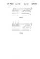
- FIG. 1 and FIG. 2are sectional views of the substrate to explain the basic idea of the method of manufacturing semiconductor devices of this invention
- FIG. 3is a sectional view of the substrate to explain one of the embodiments of this invention.
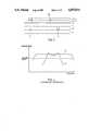
- FIG. 4is a temperature distribution diagram in an annealing process
- FIG. 5is a sectional view of the substrate to explain the recrystallization process of the same embodiment as shown in FIG. 3;
- FIG. 6is a sectional view of the substrate to explain a different embodiment of this invention.
- Monocrystallizationmay be achieved by providing an amorphous or polycrystalline thin film with energy by radiating with laser beams, electron beams or the like to dissolve it once, and controlling the temperature distribution and the nucleus generating position when this dissolved portion is solidified.
- FIG. 1is a sectional view of the substrate to illustrate the basic idea of this monocrystallization method
- a monocrystalline substrate 11 made of silicon or other materialis used as a support stand, and an insulation film 12 made of SiO 2 , Si 3 N 4 or similar material is formed on the surface of this monocrystalline substrate 11, and a polycrystalline silicon film 13 for monocrystallizing is formed on the surface of this insulation film 12, while an insulation film made of SiO 2 , Si 3 N 4 or similar material is formed on the surface of this polycrystalline silicon film 13, a polycrystalline silicon film 15 and a belt-shaped compound film 17 of a high melting point metal film 16 made of molybdenum (Mo), tungsten (W) or other material are formed on the surface of this insulation film 14.
- the width of this belt-shaped compound film 17is smaller than the diameter of electron beams, and it is set, for example, at 10 to 20 ⁇ m.
- the substrate composed of such a laminate structureis irradiated with electron beams to be provided with energy to monocrystallize a polycrystalline region 13.
- the electron beamsheat the moncrystalline silicon film 13 only through the insulation film 14, but beneath the compound film 17, since the electron reflectivity and inhibiting ability of the high melting point metal film 16 are high, the energy of the electron beams is decreased by reflection, and it is fully absorbed within the thin film 17 so that the thin film 17 itself rises in temperature, and this heat is conducted to heat the thin film 13.
- the belt-shaped compound film 17arrests temperature rise of the amorphous thin film 13 to produce a temperature profile lower in the middle of the dissolved portion than in the peripheral portions as indicated by curve A in FIG. 4. Therefore, in the stage of dissolving and recrystallizing, it serves to present a solid-liquid boundary shape and nucleus generating position suited to monocrystallization.
- the polycrystalline silicon film 15alleviates the thermal stress occurring between the insulation film 14 and the high melting point metal film 16 at the time of heating.
- the filmsare designed so that the polycrystalline silicon film 13 is in a portion not covered by the belt-shaped compound film 17 near the end of the belt-shaped compound film 17 which is the starting point of monocrystallization.
- the film 13is caused to contact the monocrystalline substrate 11 directly, and the polycrystalline silicon film 13 beneath the belt-shaped compound film 17 grows in a process of crystallization from the seeds of the monocrystals having the same crystalline configuration as the monocrystalline substrate 11 developed by epitaxial growth from the monocrystalline substrate 11 in that portion, and the monocrystals are formed so that the configuration may be same as that of the substrate 11.
- FIG. 2is a sectional view of the substrate in another embodiment applying the same method of manufacturing semiconductor devices, in which the compound film 17 is patterned in the shape of a line and spaces, the film having a width of about 10 ⁇ m to 20 ⁇ m, and the space width being about 5 ⁇ m.
- the temperature distributionis controlled by the electron beam absorbing films 17 in the same manner as in the case shown in FIG. 1, and a plurality of monocrystalline regions are formed.
- the monocrystalline regionsare linked by forming the line-and-space pattern using the values designated above, and the crystalline configuration of the monocrystalline regions is the same as that of the monocrystalline substrate 11 as in FIG. 1, so that crystalline boundary is not formed between adjacent monocrystals. As a result, a large-area monocrystal nearly the same in width as the pseudoline electron beam is formed.
- the surface areais large in the portion contacting the monocrystalline substrate 11 which is high in heat conduction, while the belt-shaped compound film 17 is not provided on the polycrystalline silicon film 13 in the contacting portion, and this film thickness is same as that of the polycrystalline silicon film 13 not contacting the monocrystalline substrate 11 near this contacting portion.
- the heat capacity of the polycrystalline silicon in this contacting portionis smaller than that of the amorphous or polycrystalline thin film not contacting the monocrystalline substrate 11 around that portion, and therefore when dissolved and recrystallized by energy beams, since this portion contacts the monocrystalline substrate 11 which is higher in thermal conductivity, the heat conduction is great. Moreover, since the heat of this portion is small, the temperature difference becomes excessive between the polycrystalline silicon film 13 in this portion and the polycrystalline silicon film 13 not contacting with the monocrystalline substrate 11 near that portion.
- This inventionis created in the light of this point, and the basic plan of the method of manufacturing semiconductor devices is improved, and is intended to present a method of manufacturing semiconductor devices capable of monocrystallizing the amorphous or polycrystalline thin film easily and reducing damage to the formed monocrystals which have excellent uniformity, as compared with the conventional methods.
- this inventionpresents a method of fabricating semiconductors by annealing an amorphous or polycrystalline thin film by energy beams so as to dissolve and recrystallize, and forming thin layer monocrystals, in which a compound film of an electron-absorbing belt-shaped high melting point metal having a width narrower than the energy beams and polycrystalline silicon is formed on the amorphous or polycrystalline thin film, and under the center line of the belt-shaped compound film at a position more than 50 to 200 ⁇ m remote from the end of this belt-shaped compound film in the scanning direction of energy beams, said amorphous or polycrystalline thin film is caused to contact a monocrystalline substrate.
- This contact shapeis a tiny spot narrower than the width of the belt-shaped compound film, and energy beams are radiated, penetrating through this belt-shaped compound film, and the beams scan parallel to the belt, starting from the point near the end of the belt-shaped compound film. Then the amorphous or polycrystalline thin film beneath the belt-shaped compound film is crystallized from the monocrystals, inheriting the crystalline configuration of the monocrystalline substrate developed by epitaxial growth of the monocrystalline substrate in the amorphous or polycrystalline thin film contacting the monocrystalline substrate near the end of belt-shaped compound film.
- the upper surface of the amorphous or polycrystalline thin filmin the portion contacting the monocrystalline substrate so as to flush with the upper surface of the amorphous or polycrystalline thin film not in contact with the monocrystalline substrate near this contacting portion.
- the position of the contacting portion of the monocrystalline substrate and the amorphous or polycrystalline thin filmis more than 50 to 200 ⁇ m remote from the end of the belt-shaped compound film in the scanning direction, so that the energy beams may reach the amorphous or polycrystalline thin film in the portion contacting with the monocrystalline substrate after heating caused by the energy beams reaches a stationary state when starting the scanning by energy beams from near the end of the belt-shaped compound film, thereby heating the amorphous or polycrystalline thin film in this contacting portion.
- the position of the amorphous or polycrystalline thin film in the contacting portionis beneath the center line of the belt-shaped compound film, and its shape is a tiny spot narrower than the width of the belt-shaped compound film, and also the upper surface of the amorphous or polycrystalline thin film in the contacting portion is flush with the upper surface of the amorphous or polycrystalline thin film in the portion not contacting with the monocrystalline substrate near said contacting portion, so that the heat capacity of the amorphous or polycrystalline thin film in the contacting portion and its upper part may be large.
- the heat flowing in the monocrystalline substratebecomes smaller, which facilitates temperature rise of the amorphous or polycrystalline thin film in the contacting portion when dissolving and recrystallizing.
- the temperature difference from the amorphous or polycrystalline thin film not contacting the monocrystalline substrate near the contacting portionbecomes small, and when a sufficient energy for dissolving the amorphous or polycrystaline thin film in the contacting portion is given, occurrence of damage of the monocrystals due to excessive rise of the temperature in the amorphous or polycrystalline thin film not contacting with the monocrystalline substrate near the contacting portion may be prevented, so that decline of uniformity due to deviation of crystalline configuration derived from such damage may be suppressed.
- the sample structureis as follows. That is, part of the amorphous thin film for monocrystallizing is caused to contact the monocrystalline substrate, and the entire surface of this amorphous thin film is covered with a relatively thin insulation film acting as protective film. Also starting from the vicinity of the contacting portion of the amorphous thin film and the monocrystalline substrate, a belt-shaped compound film of high melting point metal such as molybdenum (Mo) and tungsten (W) and polycrystalline silicon narrower than the diameter of electron beams is laminated, and a sample substrate is prepared.
- Momolybdenum
- Wtungsten
- the position of the amorphous thin film contacting with the monocrystalline substrateis 50 to 200 ⁇ m distant from the end of the belt-shaped compound film in the scanning direction of the beams and beneath the center line of the belt-shaped compound film, and its shape is a tiny spot smaller than the width of the belt-shaped compound film.
- the upper surface of the amorphous thin film in the contacting portionis flush with the upper surface of the amorphous thin film not contacting the monocrystalline substrate near this contacting portion, so that the temperature rise of the amorphous thin film in the contacting portion is facilitated and so that the temperature difference from the amorphous thin film not contacting with the monocrystalline substrate but near the contacting portion is reduced.
- a temperature distribution optimum for monocrystalline growthis created in the same method as stated above, and by causing the amorphous thin film to contact the monocrystalline substrate at the starting point of the formation of monocrystals near the end part beneath the belt-shaped compound film, monocrystals are formed in the same crystalline configuration as in the substrate at the time of crystal growth of the amorphous thin film beneath the belt-shaped compound thin film, starting from the monocrystals in the same crystalline configuration as in the monocrystalline substrate generated by the epitaxial growth from the monocrystalline substrate in that portion.
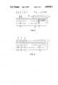
- FIG. 3is a sectional view of the substrate to explain another embodiment of this invention, in which the section in the orthogonal direction is indicated on the right and left.
- the right side of FIG. 3indicates the vicinity of the starting point of energy beam scanning near the end of the belt-shaped compound film.
- an insulation film 2 made of SiO 2 , Si 3 N 4 or similar materialis formed on a monocrystalline substrate 1 made of silicon or other material, and an opening 3 to trigger epitaxial growth from the substrate at the time of dissolving and recrystallizing is provided in part of this insulation film 2, and an opening seed is formed by exposing the substrate 1.
- an amorphous or polycrystalline silicon film 4 for monocrystallizingis formed on the surface of this insulation film 2 and substrate exposed portion at opening 3.
- the amorphous or polycrystalline silicon film 4is formed so that the upper surface of the amorphous or polycrystalline silicon film contacting with the monocrystalline substrate 1 may be flush with the upper surface of the amorphous or polycrystalline silicon film not contacting with the substrate near this contacting portion.
- an insulation film 5 made of SiO 2 , Si 3 N 4 or similar materialis formed, and in the portion containing the opening seed 3 where the polycrystalline silicon film 4 beneath the insulation film 5 on the surface of this insulation film 5 contacts the substrate, a compound film 8 is formed.
- the compound film 8is a polycrystalline silicon film 6 to alleviate the thermal stress when annealing, and a high melting point metal film 7 made of molybdenum (Mo), tungsten (W) or other material which is large in electron inhibiting ability and is high in electron reflectivity is formed.
- the compound film 8 formed from the high melting point metal film 7 and polycrystalline silicon film 6is patterned in a belt shape, and this belt width is smaller than the diameter the electron beams, for example, being set in a range of 10 to 20 ⁇ m.
- the compound film 8is patterned so that the position of the opening seed 3 contacting the monocrystalline substrate 1 and amorphous or polycrystalline silicon film 4 may be located beneath the center line of the inside belt-shaped compound film 8 more than 50 to 200 ⁇ m remote from the end 8a of the belt-shaped compound film 8 in the scanning direction of energy beams, and the shape of the opening seed 3 is formed narrower than the width of the belt-shaped compound film 8 to be, for example, a spot opening about 2 to 5 ⁇ m in diameter.
- the belt-shaped compound film 8controls the temperature rise of the polycrystalline silicon film 4 to produce a temperature profile lower in the middle part than in the peripheral parts as indicated by curve A in FIG. 4, thereby presenting an optimum temperature profile suited to induce monocrystalline growth at the time of dissolving and recrystallizing.
- this compound film 8prevents the electrons from reaching directly near the portion to be monocrystallized, it is effective in decreasing electron beam damage of the monocrystallized film.
- the temperature distribution suited to monocrystallizationis presented by the temperature distribution control by the belt-shaped compound film 8.
- the polycrystalline silicon film 4contacts the monocrystalline substrate 1 and opening seed 3
- monocrystals inheriting the crystalline configuration of the monocrystalline substrate 1are formed in this part by the epitaxial growth from the monocrystalline substrate 1 at the time of dissolving and recrystallizing, and they become seed crystals for monocrystalline growth of the polycrystalline silicon film 4 beneath the belt-shaped compound film 8, thereby enabling the control of the crystalline configuration.
- the position of the opening seed 3 contacting the monocrystalline substrate 1 and polycrystalline silicon film 4is beneath the center line of the belt-shaped compound film 8 at a position of 50 to 200 ⁇ m from the end 8a of the belt-shaped compound film 8 in the scanning direction of the energy beams, and its shape is narrower than the width of the belt-shaped compound film 8, for example, about 2 to 5 ⁇ m, and also the upper surface of the polycrystalline silicon not contacting the monocrystalline substrate 1 is flush with the upper surface of the polycrystalline silicon in the portion of the opening seed 3, the temperature rise of the polycrystalline silicon in this contacting portion is facilitated at the time of dissolving and recrystallizing, and the temperature difference from the polycrystalline silicon not contacting with the monocrystalline substrate 1 near this contacting portion is reduced.
- the thickness of the electron beam absorbing compound film 8is set to such a dimension that it is greater than the range of electrons and is enough to absorb 100% of the energy of the electrons within the film and to suppress peeling of the electron absorbing film 8 due to thermal stress at the time of annealing.
- molybdenumMo
- the range of electronsis considered around 500 nm and the electron inhibiting ability of the polycrystalline silicon is considered to be about 1/5 that of molybdenum
- the thickness of the molybdenumis set at 400 to 600 nm and that of polycrystalline silicon film at 500 to 1,000 nm, considering the suppression of molybdenum peeling and the control effect of temperature distribution by heat conduction within the electron beam absorbing film 8.
- the insulation film 5 covering the thin film 4possesses the effect of delaying the heat conduction from the electron absorbing film 8, the effect of preventing damage due to direct entrance of electron beams into the thin film 4, and the effect of preventing contamination due to direct contact with the electron beam absorbing film 8.
- the thickness of the insulation film 5is set at 400 to 600 nm in order to lower the temperature beneath the thin film 8 due to heat conduction in the insulation film 5 due to the heat generated by the thin film 8.
- FIG. 5is a sectional view of the substrate to explain the recrystallization process of an embodiment of this invention, in which illustrative sections in orthogonal directions are indicated on the right and left. Therefore, when the beam scanning is done in the rightward direction in the right-side drawing, the beam scanning is done in the direction perpendicular to the paper surface in the left-side drawing.
- electron beams 9are emitted to the substrate to the laminate structure so that the center of the electron beams 9 may be located in the middle of the electron beam absorbing film 8 penetrating through the electron beam absorbing film 8, and the electron beams 9 are scanned parallel to the belt-shaped electron beam absorbing film 8, starting from the vicinity of the end 8a of the electron beam absorbing film 8.
- monocrystals in the same crystalline configuration as in the monocrystalline substrate 1are formed by epitaxial growth from the monocrystalline substrate 1, and due to the difference in the heat conduction to the part 4-1 of the polycrystalline silicon film 4 and to the lower part of part 4-2 of the polycrystalline silicon film 4 and the temperature gradient in the horizontal direction occurring due to the scanning of the electron beams 9, the monocrystals formed in the part 4-1 are extended to the part 4-2, thereby forming seed crystals for crystal growth of the part 4-2 of the polycrystalline silicon.
- the position of part 4-1(opening seed) is located at a position of about 50 to 200 ⁇ m from the end 8a of the electron beam absorbing belt-shaped compound film 8 in the scanning direction, when the electron beams 9 are scanned starting from the vicinity of the end 8a of the electron beam absorbing film 8, the electron beams 9 may reach the part 4-1 only after reaching the thermally stationary state, and also because the part 4-1 is beneath the center line of the electron beam absorbing film 8 and its shape is narrower than the width of the electron beam absorbing film 8, being formed, for example, in a spot of about 2 to 5 ⁇ m in diameter, and moreover the upper surface of the part 4-1 is formed to be flush with the upper surface of the part 4-2, the heat capacity of the part 4-1 and its upper part is large and the heat flowing into the monocrystalline substrate 1 having a large heat conductivity becomes smaller, so that the temperature rise of the part 4-1 may be facilitated and the temperature difference between the part 4-1 and part 4-2 is reduced.
- the portion not covered with the electron beam absorbing film 8receives the electron beams 5 through the insulation film 5, and the temperature of this portion goes up.
- part of the electron beams 9is reflected, while the remainder is absorbed by the electron beam absorbing film 8, so that the temperature of the electron beam absorbing film 8 goes up, and this heat is conducted to the part 4-2 of the polycrystalline silicon film 5 through the insulation film 5.
- monocrystalsare formed in the same crystalline configuration as in the monocrystalline substrate 1, starting from the monocrystals in the same crystalline configuration as in the monocrystalline substrate 1 which have been developed by epitaxial growth from the monocrystalline substrate 1 in the part 4-1 of the polycrystalline silicon film 4 and extended toward the part 4-2.
- the stability of monocrystalline growth starting from the monocrystals of the part 4-2 of the polycrystalline silicon 4 generated in part 4-1is enhanced as compared with that in the usual lateral seeding epitaxial growth without using electron beam absorbing film 8.
- the electron beam absorbing film 8 and insulation film 5are removed by etching, and, for example, by photolithography, a monocrystalline region is processed in a shape presented for fabrication of semiconductor element.
- FIG. 6is a sectional view of the substrate to explain a further different embodiment of this invention, in which the same parts as in FIG. 3 are identified with same part numbers. It shows a substrate structure for producing large-area monocrystals having as nearly the same width as the pseudoline electron beam by annealing with pseudoline electron beams.
- an electron beam absorbing film 8 of a similar belt shape as used in the preceding embodimentsis formed in line-and-space shape.
- the lineis set at about 10 to 20 ⁇ m, and the space, about 5 ⁇ m.
- the pseudoline electron beamshave an acceleration voltage of 5 to 10 kV, and a beam current of about 1.0 to 5.0 mA, and the spot-shaped electron beams having a gaussian energy distribution of beam diameter of about 100 to 200 ⁇ m are formed in an alternating-current voltage waveform such as a triangular wave (the triangular wave frequency about 100 kHz to 50 MHz) by deflecting at a width of about 500 to 2,000 ⁇ m in the direction vertical to the scanning direction, so that, in this case, a broad and uniform temperature distribution is realized as indicated by curve B in FIG.
Landscapes
- Engineering & Computer Science (AREA)
- Physics & Mathematics (AREA)
- Computer Hardware Design (AREA)
- Microelectronics & Electronic Packaging (AREA)
- Power Engineering (AREA)
- Condensed Matter Physics & Semiconductors (AREA)
- General Physics & Mathematics (AREA)
- Manufacturing & Machinery (AREA)
- Chemical & Material Sciences (AREA)
- High Energy & Nuclear Physics (AREA)
- Crystallography & Structural Chemistry (AREA)
- Toxicology (AREA)
- Health & Medical Sciences (AREA)
- Electromagnetism (AREA)
- Optics & Photonics (AREA)
- Materials Engineering (AREA)
- Recrystallisation Techniques (AREA)
Abstract
Description
Claims (13)
Applications Claiming Priority (2)
| Application Number | Priority Date | Filing Date | Title |
|---|---|---|---|
| JP61014267AJPH0732124B2 (en) | 1986-01-24 | 1986-01-24 | Method for manufacturing semiconductor device |
| JP61-14267 | 1986-01-24 |
Publications (1)
| Publication Number | Publication Date |
|---|---|
| US4855014Atrue US4855014A (en) | 1989-08-08 |
Family
ID=11856314
Family Applications (1)
| Application Number | Title | Priority Date | Filing Date |
|---|---|---|---|
| US07/006,363Expired - LifetimeUS4855014A (en) | 1986-01-24 | 1987-01-23 | Method for manufacturing semiconductor devices |
Country Status (3)
| Country | Link |
|---|---|
| US (1) | US4855014A (en) |
| EP (1) | EP0231115B1 (en) |
| JP (1) | JPH0732124B2 (en) |
Cited By (41)
| Publication number | Priority date | Publication date | Assignee | Title |
|---|---|---|---|---|
| GB2241114A (en)* | 1990-02-16 | 1991-08-21 | Mitsubishi Electric Corp | Method of producing soi structures |
| US5075243A (en)* | 1989-08-10 | 1991-12-24 | The United States Of America As Represented By The Administrator Of The National Aeronautics And Space Administration | Fabrication of nanometer single crystal metallic CoSi2 structures on Si |
| US5236544A (en)* | 1989-06-26 | 1993-08-17 | Canon Kabushiki Kaisha | Process for growing crystal |
| US5312771A (en)* | 1990-03-24 | 1994-05-17 | Canon Kabushiki Kaisha | Optical annealing method for semiconductor layer and method for producing semiconductor device employing the same semiconductor layer |
| WO1997045827A1 (en)* | 1996-05-28 | 1997-12-04 | The Trustees Of Columbia University In The City Of New York | Crystallization processing of semiconductor film regions on a substrate, and devices made therewith |
| US6426532B1 (en) | 1998-06-30 | 2002-07-30 | Sharp Kabushiki Kaisha | Semiconductor device and method of manufacture thereof |
| US20020101178A1 (en)* | 2000-12-29 | 2002-08-01 | Jae Yong Park | Active matrix organic electroluminescence display device and method for manufacturing the same |
| US20030096489A1 (en)* | 1999-09-03 | 2003-05-22 | Im James S. | Methods for producing uniform large-grained and grain boundary location manipulated polycrystalline thin film semiconductors using sequential lateral solidification |
| US20040061843A1 (en)* | 2000-11-27 | 2004-04-01 | Im James S. | Process and mask projection system for laser crystallization processing of semiconductor film regions on a substrate |
| US20050032249A1 (en)* | 2000-03-21 | 2005-02-10 | Im James S. | Surface planarization of thin silicon films during and after processing by the sequential lateral solidification method |
| US20050034653A1 (en)* | 2001-08-27 | 2005-02-17 | James Im | Polycrystalline tft uniformity through microstructure mis-alignment |
| US20050059265A1 (en)* | 2003-09-16 | 2005-03-17 | The Trustees Of Columbia University In The City Of New York | Systems and methods for processing thin films |
| US20050059223A1 (en)* | 2003-09-16 | 2005-03-17 | The Trustees Of Columbia University | Laser-irradiated thin films having variable thickness |
| US20050059224A1 (en)* | 2003-09-16 | 2005-03-17 | The Trustees Of Columbia University In The City Of New York | Systems and methods for inducing crystallization of thin films using multiple optical paths |
| US20050202654A1 (en)* | 2002-08-19 | 2005-09-15 | Im James S. | Process and system for laser crystallization processing of film regions on a substrate to provide substantial uniformity, and a structure of such film regions |
| US20050235903A1 (en)* | 2003-09-19 | 2005-10-27 | The Trustees Of Columbia University In The City Of New York | Single scan irradiation for crystallization of thin films |
| US20060006464A1 (en)* | 2002-04-01 | 2006-01-12 | Im James S | Method and system for providing a thin film with a controlled crystal orientation using pulsed laser induced melting and nucleation-initiated crystallization |
| US20060030164A1 (en)* | 2002-08-19 | 2006-02-09 | Im James S | Process and system for laser crystallization processing of film regions on a substrate to minimize edge areas, and a structure of such film regions |
| US20060060130A1 (en)* | 2002-08-19 | 2006-03-23 | Im James S | Process and system for laser crystallization processing of film regions on a substrate to provide substantial uniformity within arears in such regions and edge areas thereof, and a structure of film regions |
| US20060134890A1 (en)* | 2003-02-19 | 2006-06-22 | Im James S | System and process for processing a plurality of semiconductor thin films which are crystallized using sequential lateral solidification techniques |
| US7115503B2 (en) | 2000-10-10 | 2006-10-03 | The Trustees Of Columbia University In The City Of New York | Method and apparatus for processing thin metal layers |
| US20070007242A1 (en)* | 2003-09-16 | 2007-01-11 | The Trustees Of Columbia University In The City Of New York | Method and system for producing crystalline thin films with a uniform crystalline orientation |
| US20070032096A1 (en)* | 2003-09-16 | 2007-02-08 | Im James S | System and process for providing multiple beam sequential lateral solidification |
| US7638728B2 (en) | 2003-09-16 | 2009-12-29 | The Trustees Of Columbia University In The City Of New York | Enhancing the width of polycrystalline grains with mask |
| US7645337B2 (en) | 2004-11-18 | 2010-01-12 | The Trustees Of Columbia University In The City Of New York | Systems and methods for creating crystallographic-orientation controlled poly-silicon films |
| US7718517B2 (en) | 2002-08-19 | 2010-05-18 | Im James S | Single-shot semiconductor processing system and method having various irradiation patterns |
| US7759230B2 (en) | 2003-09-16 | 2010-07-20 | The Trustees Of Columbia University In The City Of New York | System for providing a continuous motion sequential lateral solidification for reducing or eliminating artifacts in overlap regions, and a mask for facilitating such artifact reduction/elimination |
| US8012861B2 (en) | 2007-11-21 | 2011-09-06 | The Trustees Of Columbia University In The City Of New York | Systems and methods for preparing epitaxially textured polycrystalline films |
| US8221544B2 (en) | 2005-04-06 | 2012-07-17 | The Trustees Of Columbia University In The City Of New York | Line scan sequential lateral solidification of thin films |
| US8415670B2 (en) | 2007-09-25 | 2013-04-09 | The Trustees Of Columbia University In The City Of New York | Methods of producing high uniformity in thin film transistor devices fabricated on laterally crystallized thin films |
| US8426296B2 (en) | 2007-11-21 | 2013-04-23 | The Trustees Of Columbia University In The City Of New York | Systems and methods for preparing epitaxially textured polycrystalline films |
| US8440581B2 (en) | 2009-11-24 | 2013-05-14 | The Trustees Of Columbia University In The City Of New York | Systems and methods for non-periodic pulse sequential lateral solidification |
| US8557040B2 (en) | 2007-11-21 | 2013-10-15 | The Trustees Of Columbia University In The City Of New York | Systems and methods for preparation of epitaxially textured thick films |
| US8569155B2 (en) | 2008-02-29 | 2013-10-29 | The Trustees Of Columbia University In The City Of New York | Flash lamp annealing crystallization for large area thin films |
| US8598588B2 (en) | 2005-12-05 | 2013-12-03 | The Trustees Of Columbia University In The City Of New York | Systems and methods for processing a film, and thin films |
| US8614471B2 (en) | 2007-09-21 | 2013-12-24 | The Trustees Of Columbia University In The City Of New York | Collections of laterally crystallized semiconductor islands for use in thin film transistors |
| US8663387B2 (en) | 2003-09-16 | 2014-03-04 | The Trustees Of Columbia University In The City Of New York | Method and system for facilitating bi-directional growth |
| US8796159B2 (en) | 2003-09-16 | 2014-08-05 | The Trustees Of Columbia University In The City Of New York | Processes and systems for laser crystallization processing of film regions on a substrate utilizing a line-type beam, and structures of such film regions |
| US8802580B2 (en) | 2008-11-14 | 2014-08-12 | The Trustees Of Columbia University In The City Of New York | Systems and methods for the crystallization of thin films |
| US9087696B2 (en) | 2009-11-03 | 2015-07-21 | The Trustees Of Columbia University In The City Of New York | Systems and methods for non-periodic pulse partial melt film processing |
| US9646831B2 (en) | 2009-11-03 | 2017-05-09 | The Trustees Of Columbia University In The City Of New York | Advanced excimer laser annealing for thin films |
Citations (10)
| Publication number | Priority date | Publication date | Assignee | Title |
|---|---|---|---|---|
| FR1592287A (en)* | 1967-11-22 | 1970-05-11 | ||
| US4352835A (en)* | 1981-07-01 | 1982-10-05 | Western Electric Co., Inc. | Masking portions of a substrate |
| US4371421A (en)* | 1981-04-16 | 1983-02-01 | Massachusetts Institute Of Technology | Lateral epitaxial growth by seeded solidification |
| JPS58191450A (en)* | 1982-04-30 | 1983-11-08 | Seiko Epson Corp | Multilayer wiring structure |
| US4534820A (en)* | 1981-10-19 | 1985-08-13 | Nippon Telegraph & Telephone Public Corporation | Method for manufacturing crystalline film |
| US4545823A (en)* | 1983-11-14 | 1985-10-08 | Hewlett-Packard Company | Grain boundary confinement in silicon-on-insulator films |
| EP0167391A2 (en)* | 1984-07-02 | 1986-01-08 | Sharp Kabushiki Kaisha | Method of manufacturing semiconductor devices |
| US4589951A (en)* | 1981-07-30 | 1986-05-20 | Fujitsu Limited | Method for annealing by a high energy beam to form a single-crystal film |
| US4674176A (en)* | 1985-06-24 | 1987-06-23 | The United States Of America As Represented By The United States Department Of Energy | Planarization of metal films for multilevel interconnects by pulsed laser heating |
| JPH06247680A (en)* | 1993-02-23 | 1994-09-06 | Katsukawa Kogyo Kk | Automatic conveying device |
- 1986
- 1986-01-24JPJP61014267Apatent/JPH0732124B2/ennot_activeExpired - Fee Related
- 1987
- 1987-01-23USUS07/006,363patent/US4855014A/ennot_activeExpired - Lifetime
- 1987-01-26EPEP87300644Apatent/EP0231115B1/ennot_activeExpired - Lifetime
Patent Citations (11)
| Publication number | Priority date | Publication date | Assignee | Title |
|---|---|---|---|---|
| FR1592287A (en)* | 1967-11-22 | 1970-05-11 | ||
| US4371421A (en)* | 1981-04-16 | 1983-02-01 | Massachusetts Institute Of Technology | Lateral epitaxial growth by seeded solidification |
| US4352835A (en)* | 1981-07-01 | 1982-10-05 | Western Electric Co., Inc. | Masking portions of a substrate |
| US4589951A (en)* | 1981-07-30 | 1986-05-20 | Fujitsu Limited | Method for annealing by a high energy beam to form a single-crystal film |
| US4534820A (en)* | 1981-10-19 | 1985-08-13 | Nippon Telegraph & Telephone Public Corporation | Method for manufacturing crystalline film |
| JPS58191450A (en)* | 1982-04-30 | 1983-11-08 | Seiko Epson Corp | Multilayer wiring structure |
| US4545823A (en)* | 1983-11-14 | 1985-10-08 | Hewlett-Packard Company | Grain boundary confinement in silicon-on-insulator films |
| EP0167391A2 (en)* | 1984-07-02 | 1986-01-08 | Sharp Kabushiki Kaisha | Method of manufacturing semiconductor devices |
| US4655850A (en)* | 1984-07-02 | 1987-04-07 | Sharp Kabushiki Kaisha | Method of forming monocrystalline thin films by parallel beam scanning of belt shaped refractory metal film on amorphous or polycrystalline layer |
| US4674176A (en)* | 1985-06-24 | 1987-06-23 | The United States Of America As Represented By The United States Department Of Energy | Planarization of metal films for multilevel interconnects by pulsed laser heating |
| JPH06247680A (en)* | 1993-02-23 | 1994-09-06 | Katsukawa Kogyo Kk | Automatic conveying device |
Non-Patent Citations (10)
| Title |
|---|
| Colinge et al., Use of Selective Annealing for Growing Very Large Grain Soi Films, Applied Physics, Letters, 44(4) Aug. 15, 1982, pp. 346 347.* |
| Colinge et al., Use of Selective Annealing for Growing Very Large Grain Soi Films, Applied Physics, Letters, 44(4) Aug. 15, 1982, pp. 346-347. |
| H. Ishiwara et al., "Recrystallization of silicon-on-Insulator . . .", Jap. Journal of Appl. Physics, vol. 24, No. 2, Feb., 1985, pp. 126-132. |
| H. Ishiwara et al., Recrystallization of silicon on Insulator . . . , Jap. Journal of Appl. Physics, vol. 24, No. 2, Feb., 1985, pp. 126 132.* |
| K. Suguro et al., "Seeding Lateral Epitaxy of Silicon . . . ," Appl. Phys. Lett., 47(1985) Oct., No. 7, pp. 695-699. |
| K. Suguro et al., Seeding Lateral Epitaxy of Silicon . . . , Appl. Phys. Lett., 47(1985) Oct., No. 7, pp. 695 699.* |
| Sakurai et al., Laser Induced Lateral Eritaxial Growth of Silicon Over Silicon Dioxide, Applied Physics Letters, Jul. 1, 1982, 41(1) pp. 64 66.* |
| Sakurai et al., Laser-Induced Lateral Eritaxial Growth of Silicon Over Silicon Dioxide, Applied Physics Letters, Jul. 1, 1982, 41(1) pp. 64-66. |
| T. Inoue et al., "Electron-Beam Recrystallized Polysilicon . . . ," Microelectronics Journal, 14 (1983) Nov.-Dec., No. 6, pp. 74-81. |
| T. Inoue et al., Electron Beam Recrystallized Polysilicon . . . , Microelectronics Journal, 14 (1983) Nov. Dec., No. 6, pp. 74 81.* |
Cited By (90)
| Publication number | Priority date | Publication date | Assignee | Title |
|---|---|---|---|---|
| US5236544A (en)* | 1989-06-26 | 1993-08-17 | Canon Kabushiki Kaisha | Process for growing crystal |
| US5075243A (en)* | 1989-08-10 | 1991-12-24 | The United States Of America As Represented By The Administrator Of The National Aeronautics And Space Administration | Fabrication of nanometer single crystal metallic CoSi2 structures on Si |
| GB2241114A (en)* | 1990-02-16 | 1991-08-21 | Mitsubishi Electric Corp | Method of producing soi structures |
| US5061655A (en)* | 1990-02-16 | 1991-10-29 | Mitsubishi Denki Kabushiki Kaisha | Method of producing SOI structures |
| GB2241114B (en)* | 1990-02-16 | 1993-09-29 | Mitsubishi Electric Corp | Method of producing soi structures |
| US5312771A (en)* | 1990-03-24 | 1994-05-17 | Canon Kabushiki Kaisha | Optical annealing method for semiconductor layer and method for producing semiconductor device employing the same semiconductor layer |
| WO1997045827A1 (en)* | 1996-05-28 | 1997-12-04 | The Trustees Of Columbia University In The City Of New York | Crystallization processing of semiconductor film regions on a substrate, and devices made therewith |
| US6322625B2 (en) | 1996-05-28 | 2001-11-27 | The Trustees Of Columbia University In The City Of New York | Crystallization processing of semiconductor film regions on a substrate, and devices made therewith |
| US7319056B2 (en) | 1996-05-28 | 2008-01-15 | The Trustees Of Columbia University In The City Of New York | Methods for producing uniform large-grained and grain boundary location manipulated polycrystalline thin film semiconductors using sequential lateral solidification |
| US8859436B2 (en) | 1996-05-28 | 2014-10-14 | The Trustees Of Columbia University In The City Of New York | Uniform large-grained and grain boundary location manipulated polycrystalline thin film semiconductors formed using sequential lateral solidification and devices formed thereon |
| US7679028B2 (en) | 1996-05-28 | 2010-03-16 | The Trustees Of Columbia University In The City Of New York | Methods for producing uniform large-grained and grain boundary location manipulated polycrystalline thin film semiconductors using sequential lateral solidification |
| US20030119286A1 (en)* | 1996-05-28 | 2003-06-26 | Im James S. | Method for producing uniform large-grained and grain boundary location manipulated polycrystalline thin film semiconductors using sequential lateral solidification |
| US20050255640A1 (en)* | 1996-05-28 | 2005-11-17 | Im James S | Methods for producing uniform large-grained and grain boundary location manipulated polycrystalline thin film semiconductors using sequential lateral solidification |
| US8278659B2 (en) | 1996-05-28 | 2012-10-02 | The Trustees Of Columbia University In The City Of New York | Uniform large-grained and grain boundary location manipulated polycrystalline thin film semiconductors formed using sequential lateral solidification and devices formed thereon |
| US8680427B2 (en) | 1996-05-28 | 2014-03-25 | The Trustees Of Columbia University In The City Of New York | Uniform large-grained and gain boundary location manipulated polycrystalline thin film semiconductors formed using sequential lateral solidification and devices formed thereon |
| US6426532B1 (en) | 1998-06-30 | 2002-07-30 | Sharp Kabushiki Kaisha | Semiconductor device and method of manufacture thereof |
| US6682966B2 (en) | 1998-06-30 | 2004-01-27 | Sharp Kabushiki Kaisha | Semiconductor device and method for producing the same |
| US7029996B2 (en) | 1999-09-03 | 2006-04-18 | The Trustees Of Columbia University In The City Of New York | Methods for producing uniform large-grained and grain boundary location manipulated polycrystalline thin film semiconductors using sequential lateral solidification |
| US20030096489A1 (en)* | 1999-09-03 | 2003-05-22 | Im James S. | Methods for producing uniform large-grained and grain boundary location manipulated polycrystalline thin film semiconductors using sequential lateral solidification |
| US7220660B2 (en) | 2000-03-21 | 2007-05-22 | The Trustees Of Columbia University In The City Of New York | Surface planarization of thin silicon films during and after processing by the sequential lateral solidification method |
| US7704862B2 (en) | 2000-03-21 | 2010-04-27 | The Trustees Of Columbia University | Surface planarization of thin silicon films during and after processing by the sequential lateral solidification method |
| US20050032249A1 (en)* | 2000-03-21 | 2005-02-10 | Im James S. | Surface planarization of thin silicon films during and after processing by the sequential lateral solidification method |
| US7709378B2 (en) | 2000-10-10 | 2010-05-04 | The Trustees Of Columbia University In The City Of New York | Method and apparatus for processing thin metal layers |
| US20090140173A1 (en)* | 2000-10-10 | 2009-06-04 | Im James S | Method and apparatus for processing thin metal layers |
| US7115503B2 (en) | 2000-10-10 | 2006-10-03 | The Trustees Of Columbia University In The City Of New York | Method and apparatus for processing thin metal layers |
| US6961117B2 (en) | 2000-11-27 | 2005-11-01 | The Trustees Of Columbia University In The City Of New York | Process and mask projection system for laser crystallization processing of semiconductor film regions on a substrate |
| US20040061843A1 (en)* | 2000-11-27 | 2004-04-01 | Im James S. | Process and mask projection system for laser crystallization processing of semiconductor film regions on a substrate |
| US6836075B2 (en) | 2000-12-29 | 2004-12-28 | Lg.Philips Lcd Co., Ltd. | Active matrix organic electroluminescence display device and method for manufacturing the same |
| US20020101178A1 (en)* | 2000-12-29 | 2002-08-01 | Jae Yong Park | Active matrix organic electroluminescence display device and method for manufacturing the same |
| US7285435B2 (en) | 2000-12-29 | 2007-10-23 | Lg.Philips Lcd Co., Ltd. | Active matrix organic electroluminescence display device and method for manufacturing the same |
| US20050034653A1 (en)* | 2001-08-27 | 2005-02-17 | James Im | Polycrystalline tft uniformity through microstructure mis-alignment |
| US7160763B2 (en) | 2001-08-27 | 2007-01-09 | The Trustees Of Columbia University In The City Of New York | Polycrystalline TFT uniformity through microstructure mis-alignment |
| US7399359B2 (en) | 2002-04-01 | 2008-07-15 | The Trustees of Columbia University in theCity of New York | Method and system for providing a thin film with a controlled crystal orientation using pulsed laser induced melting and nucleation-initiated crystallization |
| US20060006464A1 (en)* | 2002-04-01 | 2006-01-12 | Im James S | Method and system for providing a thin film with a controlled crystal orientation using pulsed laser induced melting and nucleation-initiated crystallization |
| US7906414B2 (en) | 2002-08-19 | 2011-03-15 | The Trustees Of Columbia University In The City Of New York | Single-shot semiconductor processing system and method having various irradiation patterns |
| US20060060130A1 (en)* | 2002-08-19 | 2006-03-23 | Im James S | Process and system for laser crystallization processing of film regions on a substrate to provide substantial uniformity within arears in such regions and edge areas thereof, and a structure of film regions |
| US7259081B2 (en) | 2002-08-19 | 2007-08-21 | Im James S | Process and system for laser crystallization processing of film regions on a substrate to provide substantial uniformity, and a structure of such film regions |
| US8411713B2 (en) | 2002-08-19 | 2013-04-02 | The Trustees Of Columbia University In The City Of New York | Process and system for laser crystallization processing of film regions on a substrate to minimize edge areas, and structure of such film regions |
| US7300858B2 (en) | 2002-08-19 | 2007-11-27 | The Trustees Of Columbia University In The City Of New York | Laser crystallization and selective patterning using multiple beamlets |
| US8883656B2 (en) | 2002-08-19 | 2014-11-11 | The Trustees Of Columbia University In The City Of New York | Single-shot semiconductor processing system and method having various irradiation patterns |
| US20050202654A1 (en)* | 2002-08-19 | 2005-09-15 | Im James S. | Process and system for laser crystallization processing of film regions on a substrate to provide substantial uniformity, and a structure of such film regions |
| US7622370B2 (en) | 2002-08-19 | 2009-11-24 | The Trustees Of Columbia University In The City Of New York | Process and system for laser crystallization processing of film regions on a substrate to minimize edge areas, and a structure of such film regions |
| US20060030164A1 (en)* | 2002-08-19 | 2006-02-09 | Im James S | Process and system for laser crystallization processing of film regions on a substrate to minimize edge areas, and a structure of such film regions |
| US7718517B2 (en) | 2002-08-19 | 2010-05-18 | Im James S | Single-shot semiconductor processing system and method having various irradiation patterns |
| US8479681B2 (en) | 2002-08-19 | 2013-07-09 | The Trustees Of Columbia University In The City Of New York | Single-shot semiconductor processing system and method having various irradiation patterns |
| US7341928B2 (en) | 2003-02-19 | 2008-03-11 | The Trustees Of Columbia University In The City Of New York | System and process for processing a plurality of semiconductor thin films which are crystallized using sequential lateral solidification techniques |
| US20060134890A1 (en)* | 2003-02-19 | 2006-06-22 | Im James S | System and process for processing a plurality of semiconductor thin films which are crystallized using sequential lateral solidification techniques |
| US7902052B2 (en) | 2003-02-19 | 2011-03-08 | The Trustees Of Columbia University In The City Of New York | System and process for processing a plurality of semiconductor thin films which are crystallized using sequential lateral solidification techniques |
| US8063338B2 (en) | 2003-09-16 | 2011-11-22 | The Trustees Of Columbia In The City Of New York | Enhancing the width of polycrystalline grains with mask |
| US9466402B2 (en) | 2003-09-16 | 2016-10-11 | The Trustees Of Columbia University In The City Of New York | Processes and systems for laser crystallization processing of film regions on a substrate utilizing a line-type beam, and structures of such film regions |
| US7691687B2 (en) | 2003-09-16 | 2010-04-06 | The Trustees Of Columbia University In The City Of New York | Method for processing laser-irradiated thin films having variable thickness |
| US20100099273A1 (en)* | 2003-09-16 | 2010-04-22 | The Trustees Of Columbia University In The City Of New York | Enhancing the width of polycrystalline grains with mask |
| US20050059223A1 (en)* | 2003-09-16 | 2005-03-17 | The Trustees Of Columbia University | Laser-irradiated thin films having variable thickness |
| US7638728B2 (en) | 2003-09-16 | 2009-12-29 | The Trustees Of Columbia University In The City Of New York | Enhancing the width of polycrystalline grains with mask |
| US7364952B2 (en) | 2003-09-16 | 2008-04-29 | The Trustees Of Columbia University In The City Of New York | Systems and methods for processing thin films |
| US7759230B2 (en) | 2003-09-16 | 2010-07-20 | The Trustees Of Columbia University In The City Of New York | System for providing a continuous motion sequential lateral solidification for reducing or eliminating artifacts in overlap regions, and a mask for facilitating such artifact reduction/elimination |
| US7318866B2 (en) | 2003-09-16 | 2008-01-15 | The Trustees Of Columbia University In The City Of New York | Systems and methods for inducing crystallization of thin films using multiple optical paths |
| US7164152B2 (en) | 2003-09-16 | 2007-01-16 | The Trustees Of Columbia University In The City Of New York | Laser-irradiated thin films having variable thickness |
| US8476144B2 (en) | 2003-09-16 | 2013-07-02 | The Trustees Of Columbia University In The City Of New York | Method for providing a continuous motion sequential lateral solidification for reducing or eliminating artifacts in edge regions, and a mask for facilitating such artifact reduction/elimination |
| US8663387B2 (en) | 2003-09-16 | 2014-03-04 | The Trustees Of Columbia University In The City Of New York | Method and system for facilitating bi-directional growth |
| US8034698B2 (en) | 2003-09-16 | 2011-10-11 | The Trustees Of Columbia University In The City Of New York | Systems and methods for inducing crystallization of thin films using multiple optical paths |
| US20070032096A1 (en)* | 2003-09-16 | 2007-02-08 | Im James S | System and process for providing multiple beam sequential lateral solidification |
| US20070111349A1 (en)* | 2003-09-16 | 2007-05-17 | James Im | Laser-irradiated thin films having variable thickness |
| US20050059224A1 (en)* | 2003-09-16 | 2005-03-17 | The Trustees Of Columbia University In The City Of New York | Systems and methods for inducing crystallization of thin films using multiple optical paths |
| US20070007242A1 (en)* | 2003-09-16 | 2007-01-11 | The Trustees Of Columbia University In The City Of New York | Method and system for producing crystalline thin films with a uniform crystalline orientation |
| US20050059265A1 (en)* | 2003-09-16 | 2005-03-17 | The Trustees Of Columbia University In The City Of New York | Systems and methods for processing thin films |
| US8796159B2 (en) | 2003-09-16 | 2014-08-05 | The Trustees Of Columbia University In The City Of New York | Processes and systems for laser crystallization processing of film regions on a substrate utilizing a line-type beam, and structures of such film regions |
| US8715412B2 (en) | 2003-09-16 | 2014-05-06 | The Trustees Of Columbia University In The City Of New York | Laser-irradiated thin films having variable thickness |
| US8445365B2 (en) | 2003-09-19 | 2013-05-21 | The Trustees Of Columbia University In The City Of New York | Single scan irradiation for crystallization of thin films |
| US7964480B2 (en) | 2003-09-19 | 2011-06-21 | Trustees Of Columbia University In The City Of New York | Single scan irradiation for crystallization of thin films |
| US7311778B2 (en) | 2003-09-19 | 2007-12-25 | The Trustees Of Columbia University In The City Of New York | Single scan irradiation for crystallization of thin films |
| US20050235903A1 (en)* | 2003-09-19 | 2005-10-27 | The Trustees Of Columbia University In The City Of New York | Single scan irradiation for crystallization of thin films |
| US8734584B2 (en) | 2004-11-18 | 2014-05-27 | The Trustees Of Columbia University In The City Of New York | Systems and methods for creating crystallographic-orientation controlled poly-silicon films |
| US7645337B2 (en) | 2004-11-18 | 2010-01-12 | The Trustees Of Columbia University In The City Of New York | Systems and methods for creating crystallographic-orientation controlled poly-silicon films |
| US8617313B2 (en) | 2005-04-06 | 2013-12-31 | The Trustees Of Columbia University In The City Of New York | Line scan sequential lateral solidification of thin films |
| US8221544B2 (en) | 2005-04-06 | 2012-07-17 | The Trustees Of Columbia University In The City Of New York | Line scan sequential lateral solidification of thin films |
| US8598588B2 (en) | 2005-12-05 | 2013-12-03 | The Trustees Of Columbia University In The City Of New York | Systems and methods for processing a film, and thin films |
| US9012309B2 (en) | 2007-09-21 | 2015-04-21 | The Trustees Of Columbia University In The City Of New York | Collections of laterally crystallized semiconductor islands for use in thin film transistors |
| US8614471B2 (en) | 2007-09-21 | 2013-12-24 | The Trustees Of Columbia University In The City Of New York | Collections of laterally crystallized semiconductor islands for use in thin film transistors |
| US8415670B2 (en) | 2007-09-25 | 2013-04-09 | The Trustees Of Columbia University In The City Of New York | Methods of producing high uniformity in thin film transistor devices fabricated on laterally crystallized thin films |
| US8557040B2 (en) | 2007-11-21 | 2013-10-15 | The Trustees Of Columbia University In The City Of New York | Systems and methods for preparation of epitaxially textured thick films |
| US8012861B2 (en) | 2007-11-21 | 2011-09-06 | The Trustees Of Columbia University In The City Of New York | Systems and methods for preparing epitaxially textured polycrystalline films |
| US8426296B2 (en) | 2007-11-21 | 2013-04-23 | The Trustees Of Columbia University In The City Of New York | Systems and methods for preparing epitaxially textured polycrystalline films |
| US8871022B2 (en) | 2007-11-21 | 2014-10-28 | The Trustees Of Columbia University In The City Of New York | Systems and methods for preparation of epitaxially textured thick films |
| US8569155B2 (en) | 2008-02-29 | 2013-10-29 | The Trustees Of Columbia University In The City Of New York | Flash lamp annealing crystallization for large area thin films |
| US8802580B2 (en) | 2008-11-14 | 2014-08-12 | The Trustees Of Columbia University In The City Of New York | Systems and methods for the crystallization of thin films |
| US9087696B2 (en) | 2009-11-03 | 2015-07-21 | The Trustees Of Columbia University In The City Of New York | Systems and methods for non-periodic pulse partial melt film processing |
| US9646831B2 (en) | 2009-11-03 | 2017-05-09 | The Trustees Of Columbia University In The City Of New York | Advanced excimer laser annealing for thin films |
| US8889569B2 (en) | 2009-11-24 | 2014-11-18 | The Trustees Of Columbia University In The City Of New York | Systems and methods for non-periodic pulse sequential lateral soldification |
| US8440581B2 (en) | 2009-11-24 | 2013-05-14 | The Trustees Of Columbia University In The City Of New York | Systems and methods for non-periodic pulse sequential lateral solidification |
Also Published As
| Publication number | Publication date |
|---|---|
| JPH0732124B2 (en) | 1995-04-10 |
| JPS62172713A (en) | 1987-07-29 |
| EP0231115A2 (en) | 1987-08-05 |
| EP0231115A3 (en) | 1988-11-02 |
| EP0231115B1 (en) | 1992-09-23 |
Similar Documents
| Publication | Publication Date | Title |
|---|---|---|
| US4855014A (en) | Method for manufacturing semiconductor devices | |
| EP0077020B1 (en) | Method of manufacturing single-crystal film | |
| US4670088A (en) | Lateral epitaxial growth by seeded solidification | |
| US4592799A (en) | Method of recrystallizing a polycrystalline, amorphous or small grain material | |
| US4596604A (en) | Method of manufacturing a multilayer semiconductor device | |
| US4576851A (en) | Semiconductor substrate | |
| JPH084067B2 (en) | Method for manufacturing semiconductor device | |
| JPH06177034A (en) | Method for growing semiconductor single crystal | |
| US5264072A (en) | Method for recrystallizing conductive films by an indirect-heating with a thermal-conduction-controlling layer | |
| KR900002686B1 (en) | Recrystalizing method for conductor film | |
| EP0167391B1 (en) | Method of manufacturing semiconductor devices | |
| US5431126A (en) | Method of forming semiconductor crystal and semiconductor device | |
| JPH027415A (en) | Formation of soi thin film | |
| US4678538A (en) | Process for the production of an insulating support on an oriented monocrystalline silicon film with localized defects | |
| JPS6147627A (en) | Manufacture of semiconductor device | |
| US5094714A (en) | Wafer structure for forming a semiconductor single crystal film | |
| JPH0442358B2 (en) | ||
| JPH0236051B2 (en) | ||
| Inoue et al. | Electron-beam recrystallization of silicon layers on silicon dioxide | |
| JPH0775223B2 (en) | Method for manufacturing semiconductor single crystal layer | |
| JP2569402B2 (en) | Manufacturing method of semiconductor thin film crystal layer | |
| JPS62179112A (en) | Formation of soi structure | |
| JPS61203629A (en) | Single crystallization method of semiconductor layer | |
| JPH0149003B2 (en) | ||
| JPH0523492B2 (en) |
Legal Events
| Date | Code | Title | Description |
|---|---|---|---|
| AS | Assignment | Owner name:SHARP KABUSHIKI KAISHA 22-22 NAGAIKE-CHO, ABENO-KU Free format text:ASSIGNMENT OF ASSIGNORS INTEREST.;ASSIGNORS:KAKIMOTO, SEIZO;KUDO, JUN;KOBA, MASAYOSHI;REEL/FRAME:004662/0411 Effective date:19870108 Owner name:SHARP KABUSHIKI KAISHA, JAPAN Free format text:ASSIGNMENT OF ASSIGNORS INTEREST;ASSIGNORS:KAKIMOTO, SEIZO;KUDO, JUN;KOBA, MASAYOSHI;REEL/FRAME:004662/0411 Effective date:19870108 | |
| STCF | Information on status: patent grant | Free format text:PATENTED CASE | |
| FEPP | Fee payment procedure | Free format text:PAYOR NUMBER ASSIGNED (ORIGINAL EVENT CODE: ASPN); ENTITY STATUS OF PATENT OWNER: LARGE ENTITY | |
| FPAY | Fee payment | Year of fee payment:4 | |
| FEPP | Fee payment procedure | Free format text:PAYER NUMBER DE-ASSIGNED (ORIGINAL EVENT CODE: RMPN); ENTITY STATUS OF PATENT OWNER: LARGE ENTITY Free format text:PAYOR NUMBER ASSIGNED (ORIGINAL EVENT CODE: ASPN); ENTITY STATUS OF PATENT OWNER: LARGE ENTITY | |
| FPAY | Fee payment | Year of fee payment:8 | |
| FPAY | Fee payment | Year of fee payment:12 |