US4854337A - Apparatus for treating wafers utilizing megasonic energy - Google Patents
Apparatus for treating wafers utilizing megasonic energyDownload PDFInfo
- Publication number
- US4854337A US4854337AUS07/197,867US19786788AUS4854337AUS 4854337 AUS4854337 AUS 4854337AUS 19786788 AUS19786788 AUS 19786788AUS 4854337 AUS4854337 AUS 4854337A
- Authority
- US
- United States
- Prior art keywords
- container
- wafers
- invention according
- transducer
- carrier
- Prior art date
- Legal status (The legal status is an assumption and is not a legal conclusion. Google has not performed a legal analysis and makes no representation as to the accuracy of the status listed.)
- Expired - Lifetime
Links
Images
Classifications
- H—ELECTRICITY
- H01—ELECTRIC ELEMENTS
- H01L—SEMICONDUCTOR DEVICES NOT COVERED BY CLASS H10
- H01L21/00—Processes or apparatus adapted for the manufacture or treatment of semiconductor or solid state devices or of parts thereof
- H01L21/67—Apparatus specially adapted for handling semiconductor or electric solid state devices during manufacture or treatment thereof; Apparatus specially adapted for handling wafers during manufacture or treatment of semiconductor or electric solid state devices or components ; Apparatus not specifically provided for elsewhere
- H01L21/67005—Apparatus not specifically provided for elsewhere
- H01L21/67011—Apparatus for manufacture or treatment
- H01L21/67017—Apparatus for fluid treatment
- H01L21/67023—Apparatus for fluid treatment for general liquid treatment, e.g. etching followed by cleaning
- B—PERFORMING OPERATIONS; TRANSPORTING
- B08—CLEANING
- B08B—CLEANING IN GENERAL; PREVENTION OF FOULING IN GENERAL
- B08B3/00—Cleaning by methods involving the use or presence of liquid or steam
- B08B3/04—Cleaning involving contact with liquid
- B08B3/10—Cleaning involving contact with liquid with additional treatment of the liquid or of the object being cleaned, e.g. by heat, by electricity or by vibration
- B08B3/12—Cleaning involving contact with liquid with additional treatment of the liquid or of the object being cleaned, e.g. by heat, by electricity or by vibration by sonic or ultrasonic vibrations
- Y—GENERAL TAGGING OF NEW TECHNOLOGICAL DEVELOPMENTS; GENERAL TAGGING OF CROSS-SECTIONAL TECHNOLOGIES SPANNING OVER SEVERAL SECTIONS OF THE IPC; TECHNICAL SUBJECTS COVERED BY FORMER USPC CROSS-REFERENCE ART COLLECTIONS [XRACs] AND DIGESTS
- Y10—TECHNICAL SUBJECTS COVERED BY FORMER USPC
- Y10S—TECHNICAL SUBJECTS COVERED BY FORMER USPC CROSS-REFERENCE ART COLLECTIONS [XRACs] AND DIGESTS
- Y10S134/00—Cleaning and liquid contact with solids
- Y10S134/902—Semiconductor wafer
Definitions
- the present inventionis directed to the field of surface cleaning and etching of wafers such as silicon substrates and, more particularly, to an improved apparatus for enhancing the process of treating a plurality of semiconductor wafers.
- the use of the high frequency, or megasonic, agitation of the solutionshas resulted in improved cleaning and etching, paticularly on wafers with very small, micron-sized components or elements thereon. Further, the use of such high frequency agitation has resulted in a gentler cleaning action on the wafers than that obtained with intermediate frequency agitation. As a result, damage to the micro-sized components during the etching and cleaning operations during the production of the semiconductor wafers has been significantly reduced with the use of high frequency agitation. The productivity of the semiconductor production system has thus been improved due to the reduction in damage to the elements on the semiconductor wafers.
- a megasonic cleaning and etching deviceobviating the foregoing problems, providing higher wafer yield with less damage to the wafers, permitting smaller space requirements and less fluid use, as well as easier transducer maintenance, will achieve widespread acceptance in the semiconductor manufacturing industry.
- the present inventionprovides apparatus for treating the surfaces of a plurality of semiconductor wafers comprising a container means arranged to hold a body of a cleaning or etching fluid.
- the containerhas an open upper side for accepting a cassette containing a plurality of vertically disposed semiconductor wafers.
- Meansis provided for supporting the cassette with the semiconductor wafers carried thereby beneath the surface of the fluid in said container.
- a transducer carrieris mounted in the container.
- the carrierhas at least one megasonic transducer arranged to project a beam of ultrasonic energy over the vertical surfaces of the semiconductor wafers, and means is provided for energizing the megasonic transducer to oscillate at a frequency of between about 0.2 and 0.5 MHz.
- Meansis also provided for moving the transducer carrier parallel with the semconductor wafer surfaces transversely of the container whereby the ultrasonic energy beam contacts and treats the entire surface of all of the semiconductor wafers therein.
- the present inventionprovides an apparatus in which the transducer may be easily and quickly serviced, without requiring that the cleaning or etching fluid be first removed from the container.
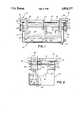
- FIG. 1is a side sectional elevation of the semiconductor treating apparatus of the present invention.
- FIG. 2is an end elevational view, partially in section, of the apparatus illustrated in FIG. 1.
- the apparatuscomprises a container means or tank 12 arranged to have an open upper surface and containing a treatment fluid for treating semiconductor wafers.
- the container meansis provided with an inlet 11 and a drain 13 for adding or removing treatment fluid, as necessary, to achieve a liquid level 14.
- the tankis provided with a flared upper edge forming a ledge 16 about the upper periphery thereof.
- the semiconductor wafers 18, shown in phantomare disposed vertically in parallel relationship in a wafer-carrying cassette supporting means 20, also shown in phantom.
- a cassette-supporting meanscomprises a plurality of transverse hanger plate members 22, arranged to be supported by the ledge 16 at the upper side of the container means 12.
- the hanger platesare spaced apart a distance slightly greater than the length of a wafer-carrying cassette and are interconnected by longitudinally extending hanger bars 24, only one of which is shown.
- a flange 26 on the outer surface of the cassette 20is arranged to engage and be supported by bars 24, supporting the semiconductor wafers 18 below the surface of the treatment fluid in the container means.
- a transducer carrier 30is suspended in the lower portion of the container tank 12 and is arranged to be moved beneath the cassettes 20 (two of which are illustrated in FIG. 1) and semiconductor wafers 18, as will be described hereinafter.
- the transducer carrieris shown as containing a pair of megasonic transducers 32, each disposed beneath a respective wafer-carrying cassette 20, substantially as illustrated.
- a cover member 34is disposed over the upper surface of the transducers 32 providing a hermetic seal for the components carried by transducer carrier 30.
- the cover 34is provided with openings 36 over each of the transducers 32 to permit the direct radiation of the ultrasonic energy therefrom upwardly into the treatment fluid.
- the transducer carrier 30extends the full length of the container tank 12 but has a width only a fraction of the width of the container.
- the transducer carrier 30is suspended above the bottom of the tank by a pair of substantially vertical tubular members 40 and 42 at opposite ends thereof.
- the tubular membersare sealed to the carrier and extend upwardly to above the top of the tank where they are hung from carriage members 44 and 46, at either end of the tank.
- a pair of rails 48 and 50are provided at each end of the tank and are arranged parallel with each other and with the bottom of the tank.
- the railsare supported by brackets 54 which extend from the tank to space the rails from the end thereof.
- Each carriage member, 44 and 46comprises an upright member 60 and 61, each carrying a set of wheels or rollers, 62 and 63 which are arranged to engage and ride on rails 48 and 50, respectively.
- Each of the upright membersextends above the upper edge of the tank 12 where it is joined to a crossover member 64 and 66.
- Each of the crossover membersextends over the top edge of the tank from the upright member 60 and 61, to the tubular members 40 and 42 which are joined thereto.
- the crossover membersare connected to the upright members with removable fasteners, such as bolts, not shown, to permit the disconnection of the crossover members from the upright members.
- a drive motor 70is arranged at one end of the tank 12 and is provided with a drive sheave 72 which engages and drives a drive belt 74.
- the drive belt 74extends across the end of the tank 12 to a return sheave 76 and is connected to the carriage member 60 by means of a clip 78.
- the megasonic transducers 32are provided with power via leads, not shown, which extend to the transducer carrier through the tubular members 40 and 42. Since the tubular members 40 and 42 are sealed at their connection with the transducer carrier 30, the leads are protected from the environment of the bath within tank 12. Suitable instrumentation and control leads may also be supplied to the transducer carrier through the tubular members.
- the tankis filled with the appropriate fluid to a level approximating that indicated at 14, and a wafer-carrying cassette 20 is lowered into the bath to be supported by the hanger rods 24 which engage the flanges 26 on the outer face of the cassette.
- the semiconductor wafers 18are thus disposed vertically in the bath above the transducer carrier 30.
- the ultrasonic transducer 32are then actuated along with the drive motor 70 which traverses the transducer carrier back and forth beneath the semiconductor wafers in the bath.
- the intense beam of megasonic wavesare projected upward from the transducers 32 and contact the surfaces of the semiconductor wafers 18 as the carrier is moved back and forth beneath the wafer-carrying cassette 20.
- the entire surface of the semiconductor waferscan be uniformly treated by the megasonic beam generated by transducers 32 without any intervention of tank walls and without unnecessary movement of the wafers in the bath.
- the drive motor 70may be controlled so as to provide non-uniform exposure of the semiconductor wafers to the ultrasonic beam. This might be necessary or desirable when it is found that the semiconductor wafers contain portions which are more difficult to clean or etch than other portions.
- the present inventionprovides a semiconductor treatment apparatus which reduces the movement of the semiconductor wafers and the attendant damage thereto, while still providing uniform exposure of the wafers to the action of the ultrasonic energy generated by the movement of the megasonic transducers through the bath beneath the wafers. Moreover, it will be seen that with the construction of the the present invention, service of the transducers is significantly improved with an attendant reduction in time and cost.
Landscapes
- Engineering & Computer Science (AREA)
- Physics & Mathematics (AREA)
- Condensed Matter Physics & Semiconductors (AREA)
- General Physics & Mathematics (AREA)
- Manufacturing & Machinery (AREA)
- Computer Hardware Design (AREA)
- Microelectronics & Electronic Packaging (AREA)
- Power Engineering (AREA)
- Weting (AREA)
- Cleaning Or Drying Semiconductors (AREA)
Abstract
Description
Claims (12)
Priority Applications (2)
| Application Number | Priority Date | Filing Date | Title |
|---|---|---|---|
| US07/197,867US4854337A (en) | 1988-05-24 | 1988-05-24 | Apparatus for treating wafers utilizing megasonic energy |
| PCT/US1989/002030WO1989011730A1 (en) | 1988-05-24 | 1989-05-12 | Apparatus for treating wafers utilizing megasonic energy |
Applications Claiming Priority (1)
| Application Number | Priority Date | Filing Date | Title |
|---|---|---|---|
| US07/197,867US4854337A (en) | 1988-05-24 | 1988-05-24 | Apparatus for treating wafers utilizing megasonic energy |
Publications (1)
| Publication Number | Publication Date |
|---|---|
| US4854337Atrue US4854337A (en) | 1989-08-08 |
Family
ID=22731061
Family Applications (1)
| Application Number | Title | Priority Date | Filing Date |
|---|---|---|---|
| US07/197,867Expired - LifetimeUS4854337A (en) | 1988-05-24 | 1988-05-24 | Apparatus for treating wafers utilizing megasonic energy |
Country Status (2)
| Country | Link |
|---|---|
| US (1) | US4854337A (en) |
| WO (1) | WO1989011730A1 (en) |
Cited By (46)
| Publication number | Priority date | Publication date | Assignee | Title |
|---|---|---|---|---|
| US4980300A (en)* | 1987-11-28 | 1990-12-25 | Kabushiki Kaisha Toshiba | Gettering method for a semiconductor wafer |
| US5013366A (en)* | 1988-12-07 | 1991-05-07 | Hughes Aircraft Company | Cleaning process using phase shifting of dense phase gases |
| DE3937442A1 (en)* | 1989-11-10 | 1991-05-16 | Nokia Unterhaltungselektronik | METHOD FOR AREA REMOVAL OF LAYERS FROM A SUBSTRATE |
| US5038808A (en)* | 1990-03-15 | 1991-08-13 | S&K Products International, Inc. | High frequency ultrasonic system |
| US5143103A (en)* | 1991-01-04 | 1992-09-01 | International Business Machines Corporation | Apparatus for cleaning and drying workpieces |
| US5148823A (en)* | 1990-10-16 | 1992-09-22 | Verteg, Inc. | Single chamber megasonic energy cleaner |
| DE9214292U1 (en)* | 1992-10-22 | 1992-12-17 | Horst Rothenberger GmbH, 3079 Warmsen | Ultrasonic cleaning device |
| US5197655A (en)* | 1992-06-05 | 1993-03-30 | International Business Machines Corporation | Fine pitch solder application |
| US5203798A (en)* | 1990-06-25 | 1993-04-20 | Hitachi, Ltd. | Cleaning apparatus for substrate |
| EP0546685A3 (en)* | 1991-11-12 | 1993-08-18 | Submicron Systems, Inc. | Megasonic cleaning system |
| US5286657A (en)* | 1990-10-16 | 1994-02-15 | Verteq, Inc. | Single wafer megasonic semiconductor wafer processing system |
| US5391511A (en)* | 1992-02-19 | 1995-02-21 | Micron Technology, Inc. | Semiconductor processing method of producing an isolated polysilicon lined cavity and a method of forming a capacitor |
| US5427622A (en)* | 1993-02-12 | 1995-06-27 | International Business Machines Corporation | Method for uniform cleaning of wafers using megasonic energy |
| US5456759A (en)* | 1992-08-10 | 1995-10-10 | Hughes Aircraft Company | Method using megasonic energy in liquefied gases |
| US5593505A (en)* | 1995-04-19 | 1997-01-14 | Memc Electronic Materials, Inc. | Method for cleaning semiconductor wafers with sonic energy and passing through a gas-liquid-interface |
| US5816274A (en)* | 1997-04-10 | 1998-10-06 | Memc Electronic Materials, Inc. | Apparartus for cleaning semiconductor wafers |
| US5834871A (en)* | 1996-08-05 | 1998-11-10 | Puskas; William L. | Apparatus and methods for cleaning and/or processing delicate parts |
| US5876507A (en)* | 1997-06-30 | 1999-03-02 | International Business Machines Corporation | Fluid treatment device and method |
| US5888124A (en)* | 1997-09-26 | 1999-03-30 | Vanguard International Semiconductor Corporation | Apparatus for polishing and cleaning a wafer |
| US6016821A (en)* | 1996-09-24 | 2000-01-25 | Puskas; William L. | Systems and methods for ultrasonically processing delicate parts |
| US6039814A (en)* | 1996-07-04 | 2000-03-21 | Tadahiro Ohmi | Cleaning method utilizing degassed cleaning liquid with applied ultrasonics |
| US6199563B1 (en)* | 1997-02-21 | 2001-03-13 | Canon Kabushiki Kaisha | Wafer processing apparatus, wafer processing method, and semiconductor substrate fabrication method |
| US6276370B1 (en) | 1999-06-30 | 2001-08-21 | International Business Machines Corporation | Sonic cleaning with an interference signal |
| US6311702B1 (en)* | 1998-11-11 | 2001-11-06 | Applied Materials, Inc. | Megasonic cleaner |
| US6313565B1 (en) | 2000-02-15 | 2001-11-06 | William L. Puskas | Multiple frequency cleaning system |
| US6314974B1 (en) | 1999-06-28 | 2001-11-13 | Fairchild Semiconductor Corporation | Potted transducer array with matching network in a multiple pass configuration |
| US6506260B1 (en)* | 1999-07-29 | 2003-01-14 | Kaneka Corporation | Method for cleaning photovoltaic module and cleaning apparatus |
| US20030015494A1 (en)* | 2001-07-20 | 2003-01-23 | Seagate Technology Llc | Single layer resist lift-off process and apparatus for submicron structures |
| US20030028287A1 (en)* | 1999-08-09 | 2003-02-06 | Puskas William L. | Apparatus, circuitry and methods for cleaning and/or processing with sound waves |
| CN1104040C (en)* | 1997-02-04 | 2003-03-26 | 佳能株式会社 | Wafer processing device, wafer transfer device, and wafer processing method |
| US6675817B1 (en)* | 1999-04-23 | 2004-01-13 | Lg.Philips Lcd Co., Ltd. | Apparatus for etching a glass substrate |
| US20040011133A1 (en)* | 2002-07-16 | 2004-01-22 | Busch Ralph E. | Ultrasonic test chamber for tray production system and the like |
| US6767840B1 (en)* | 1997-02-21 | 2004-07-27 | Canon Kabushiki Kaisha | Wafer processing apparatus, wafer processing method, and semiconductor substrate fabrication method |
| US20040206180A1 (en)* | 2002-07-16 | 2004-10-21 | Busch Ralph E. | Pulse echo ultrasonic test chamber for tray production system |
| US20040256952A1 (en)* | 1996-09-24 | 2004-12-23 | William Puskas | Multi-generator system for an ultrasonic processing tank |
| US20050017599A1 (en)* | 1996-08-05 | 2005-01-27 | Puskas William L. | Apparatus, circuitry, signals and methods for cleaning and/or processing with sound |
| US20050257617A1 (en)* | 2004-05-24 | 2005-11-24 | Busch Ralph E | Method and apparatus for ultrasonic scanning of a fabrication wafer |
| US20060086604A1 (en)* | 1996-09-24 | 2006-04-27 | Puskas William L | Organism inactivation method and system |
| US20070205695A1 (en)* | 1996-08-05 | 2007-09-06 | Puskas William L | Apparatus, circuitry, signals, probes and methods for cleaning and/or processing with sound |
| US7336019B1 (en) | 2005-07-01 | 2008-02-26 | Puskas William L | Apparatus, circuitry, signals, probes and methods for cleaning and/or processing with sound |
| US20080047575A1 (en)* | 1996-09-24 | 2008-02-28 | Puskas William L | Apparatus, circuitry, signals and methods for cleaning and processing with sound |
| US20080178911A1 (en)* | 2006-07-21 | 2008-07-31 | Christopher Hahn | Apparatus for ejecting fluid onto a substrate and system and method incorporating the same |
| US20090049908A1 (en)* | 2007-08-24 | 2009-02-26 | Bandelin Electronic Gmbh & Co. Kg | Device And Method For Qualitative Determination Of The Cavitation Energy Of Ultrasound In Containers |
| US7518288B2 (en) | 1996-09-30 | 2009-04-14 | Akrion Technologies, Inc. | System for megasonic processing of an article |
| US7917317B2 (en) | 2006-07-07 | 2011-03-29 | Sonix, Inc. | Ultrasonic inspection using acoustic modeling |
| US10512946B2 (en)* | 2015-09-03 | 2019-12-24 | Taiwan Semiconductor Manufacturing Co., Ltd. | Gigasonic cleaning techniques |
Citations (2)
| Publication number | Priority date | Publication date | Assignee | Title |
|---|---|---|---|---|
| US4705054A (en)* | 1985-08-15 | 1987-11-10 | Fields John T | Ultrasonic radiator cleaning system |
| US4736760A (en)* | 1986-02-21 | 1988-04-12 | Robert A. Coberly | Apparatus for cleaning, rinsing and drying substrates |
Family Cites Families (6)
| Publication number | Priority date | Publication date | Assignee | Title |
|---|---|---|---|---|
| US3240963A (en)* | 1962-01-04 | 1966-03-15 | Coal Res Inst | Apparatus for generating ultrasonic vibrations in liquids |
| US3198489A (en)* | 1962-02-16 | 1965-08-03 | Birtcher Corp | Compound ultrasonic transducer and mounting means therefor |
| DE1206263B (en)* | 1962-12-05 | 1965-12-02 | Wenczler & Heidenhain | Ultrasonic cleaning system |
| US3893869A (en)* | 1974-05-31 | 1975-07-08 | Rca Corp | Megasonic cleaning system |
| US4401131A (en)* | 1981-05-15 | 1983-08-30 | Gca Corporation | Apparatus for cleaning semiconductor wafers |
| US4602184A (en)* | 1984-10-29 | 1986-07-22 | Ford Motor Company | Apparatus for applying high frequency ultrasonic energy to cleaning and etching solutions |
- 1988
- 1988-05-24USUS07/197,867patent/US4854337A/ennot_activeExpired - Lifetime
- 1989
- 1989-05-12WOPCT/US1989/002030patent/WO1989011730A1/enunknown
Patent Citations (2)
| Publication number | Priority date | Publication date | Assignee | Title |
|---|---|---|---|---|
| US4705054A (en)* | 1985-08-15 | 1987-11-10 | Fields John T | Ultrasonic radiator cleaning system |
| US4736760A (en)* | 1986-02-21 | 1988-04-12 | Robert A. Coberly | Apparatus for cleaning, rinsing and drying substrates |
Cited By (81)
| Publication number | Priority date | Publication date | Assignee | Title |
|---|---|---|---|---|
| US6288476B1 (en) | 1981-02-10 | 2001-09-11 | William L. Puskas | Ultrasonic transducer with bias bolt compression bolt |
| US4980300A (en)* | 1987-11-28 | 1990-12-25 | Kabushiki Kaisha Toshiba | Gettering method for a semiconductor wafer |
| US5013366A (en)* | 1988-12-07 | 1991-05-07 | Hughes Aircraft Company | Cleaning process using phase shifting of dense phase gases |
| DE3937442A1 (en)* | 1989-11-10 | 1991-05-16 | Nokia Unterhaltungselektronik | METHOD FOR AREA REMOVAL OF LAYERS FROM A SUBSTRATE |
| US5038808A (en)* | 1990-03-15 | 1991-08-13 | S&K Products International, Inc. | High frequency ultrasonic system |
| US5203798A (en)* | 1990-06-25 | 1993-04-20 | Hitachi, Ltd. | Cleaning apparatus for substrate |
| US5148823A (en)* | 1990-10-16 | 1992-09-22 | Verteg, Inc. | Single chamber megasonic energy cleaner |
| US5286657A (en)* | 1990-10-16 | 1994-02-15 | Verteq, Inc. | Single wafer megasonic semiconductor wafer processing system |
| US5143103A (en)* | 1991-01-04 | 1992-09-01 | International Business Machines Corporation | Apparatus for cleaning and drying workpieces |
| EP0546685A3 (en)* | 1991-11-12 | 1993-08-18 | Submicron Systems, Inc. | Megasonic cleaning system |
| US5391511A (en)* | 1992-02-19 | 1995-02-21 | Micron Technology, Inc. | Semiconductor processing method of producing an isolated polysilicon lined cavity and a method of forming a capacitor |
| US5197655A (en)* | 1992-06-05 | 1993-03-30 | International Business Machines Corporation | Fine pitch solder application |
| US5456759A (en)* | 1992-08-10 | 1995-10-10 | Hughes Aircraft Company | Method using megasonic energy in liquefied gases |
| DE9214292U1 (en)* | 1992-10-22 | 1992-12-17 | Horst Rothenberger GmbH, 3079 Warmsen | Ultrasonic cleaning device |
| US5427622A (en)* | 1993-02-12 | 1995-06-27 | International Business Machines Corporation | Method for uniform cleaning of wafers using megasonic energy |
| US5579792A (en)* | 1993-02-12 | 1996-12-03 | International Business Machines Corporation | Apparatus for uniform cleaning of wafers using megasonic energy |
| US5626159A (en)* | 1995-04-19 | 1997-05-06 | Memc Electronic Materials, Inc. | Apparatus for cleaning semiconductor wafers |
| US5593505A (en)* | 1995-04-19 | 1997-01-14 | Memc Electronic Materials, Inc. | Method for cleaning semiconductor wafers with sonic energy and passing through a gas-liquid-interface |
| US6039814A (en)* | 1996-07-04 | 2000-03-21 | Tadahiro Ohmi | Cleaning method utilizing degassed cleaning liquid with applied ultrasonics |
| US20070205695A1 (en)* | 1996-08-05 | 2007-09-06 | Puskas William L | Apparatus, circuitry, signals, probes and methods for cleaning and/or processing with sound |
| US6946773B2 (en) | 1996-08-05 | 2005-09-20 | Puskas William L | Apparatus and methods for cleaning and/or processing delicate parts |
| US6002195A (en)* | 1996-08-05 | 1999-12-14 | Puskas; William L. | Apparatus and methods for cleaning and/or processing delicate parts |
| US20050017599A1 (en)* | 1996-08-05 | 2005-01-27 | Puskas William L. | Apparatus, circuitry, signals and methods for cleaning and/or processing with sound |
| US6914364B2 (en) | 1996-08-05 | 2005-07-05 | William L. Puskas | Apparatus and methods for cleaning and/or processing delicate parts |
| US20040182414A1 (en)* | 1996-08-05 | 2004-09-23 | Puskas William L. | Apparatus and methods for cleaning and/or processing delicate parts |
| US6181051B1 (en) | 1996-08-05 | 2001-01-30 | William L. Puskas | Apparatus and methods for cleaning and/or processing delicate parts |
| US8075695B2 (en) | 1996-08-05 | 2011-12-13 | Puskas William L | Apparatus, circuitry, signals, probes and methods for cleaning and/or processing with sound |
| US7211928B2 (en) | 1996-08-05 | 2007-05-01 | Puskas William L | Apparatus, circuitry, signals and methods for cleaning and/or processing with sound |
| US6538360B2 (en) | 1996-08-05 | 2003-03-25 | William L. Puskas | Multiple frequency cleaning system |
| US6433460B1 (en) | 1996-08-05 | 2002-08-13 | William L. Puskas | Apparatus and methods for cleaning and/or processing delicate parts |
| US5834871A (en)* | 1996-08-05 | 1998-11-10 | Puskas; William L. | Apparatus and methods for cleaning and/or processing delicate parts |
| US20020171331A1 (en)* | 1996-08-05 | 2002-11-21 | Puskas William L. | Apparatus and methods for cleaning and/or processing delicate parts |
| US6242847B1 (en) | 1996-09-24 | 2001-06-05 | William L. Puskas | Ultrasonic transducer with epoxy compression elements |
| US6172444B1 (en) | 1996-09-24 | 2001-01-09 | William L. Puskas | Power system for impressing AC voltage across a capacitive element |
| US20060086604A1 (en)* | 1996-09-24 | 2006-04-27 | Puskas William L | Organism inactivation method and system |
| US7004016B1 (en) | 1996-09-24 | 2006-02-28 | Puskas William L | Probe system for ultrasonic processing tank |
| US7211927B2 (en) | 1996-09-24 | 2007-05-01 | William Puskas | Multi-generator system for an ultrasonic processing tank |
| US6016821A (en)* | 1996-09-24 | 2000-01-25 | Puskas; William L. | Systems and methods for ultrasonically processing delicate parts |
| US20040256952A1 (en)* | 1996-09-24 | 2004-12-23 | William Puskas | Multi-generator system for an ultrasonic processing tank |
| US20080047575A1 (en)* | 1996-09-24 | 2008-02-28 | Puskas William L | Apparatus, circuitry, signals and methods for cleaning and processing with sound |
| US8257505B2 (en) | 1996-09-30 | 2012-09-04 | Akrion Systems, Llc | Method for megasonic processing of an article |
| US7518288B2 (en) | 1996-09-30 | 2009-04-14 | Akrion Technologies, Inc. | System for megasonic processing of an article |
| US8771427B2 (en) | 1996-09-30 | 2014-07-08 | Akrion Systems, Llc | Method of manufacturing integrated circuit devices |
| CN1104040C (en)* | 1997-02-04 | 2003-03-26 | 佳能株式会社 | Wafer processing device, wafer transfer device, and wafer processing method |
| EP0860860A3 (en)* | 1997-02-21 | 2001-11-28 | Canon Kabushiki Kaisha | Wafer processing apparatus, wafer processing method, and semiconductor substrate fabrication method |
| CN1111900C (en)* | 1997-02-21 | 2003-06-18 | 佳能株式会社 | Chip processing device, wafer processing and preparation method of semiconductor substrate |
| US6767840B1 (en)* | 1997-02-21 | 2004-07-27 | Canon Kabushiki Kaisha | Wafer processing apparatus, wafer processing method, and semiconductor substrate fabrication method |
| US6199563B1 (en)* | 1997-02-21 | 2001-03-13 | Canon Kabushiki Kaisha | Wafer processing apparatus, wafer processing method, and semiconductor substrate fabrication method |
| US5816274A (en)* | 1997-04-10 | 1998-10-06 | Memc Electronic Materials, Inc. | Apparartus for cleaning semiconductor wafers |
| US5876507A (en)* | 1997-06-30 | 1999-03-02 | International Business Machines Corporation | Fluid treatment device and method |
| US5888124A (en)* | 1997-09-26 | 1999-03-30 | Vanguard International Semiconductor Corporation | Apparatus for polishing and cleaning a wafer |
| US6311702B1 (en)* | 1998-11-11 | 2001-11-06 | Applied Materials, Inc. | Megasonic cleaner |
| US6675817B1 (en)* | 1999-04-23 | 2004-01-13 | Lg.Philips Lcd Co., Ltd. | Apparatus for etching a glass substrate |
| US6314974B1 (en) | 1999-06-28 | 2001-11-13 | Fairchild Semiconductor Corporation | Potted transducer array with matching network in a multiple pass configuration |
| US6399022B1 (en) | 1999-06-28 | 2002-06-04 | Fairchild Semiconductor Corporation | Simplified ozonator for a semiconductor wafer cleaner |
| US6367493B2 (en) | 1999-06-28 | 2002-04-09 | Fairchild Semiconductor Corporation | Potted transducer array with matching network in a multiple pass configuration |
| US6276370B1 (en) | 1999-06-30 | 2001-08-21 | International Business Machines Corporation | Sonic cleaning with an interference signal |
| US6506260B1 (en)* | 1999-07-29 | 2003-01-14 | Kaneka Corporation | Method for cleaning photovoltaic module and cleaning apparatus |
| US20030028287A1 (en)* | 1999-08-09 | 2003-02-06 | Puskas William L. | Apparatus, circuitry and methods for cleaning and/or processing with sound waves |
| US6822372B2 (en) | 1999-08-09 | 2004-11-23 | William L. Puskas | Apparatus, circuitry and methods for cleaning and/or processing with sound waves |
| US6313565B1 (en) | 2000-02-15 | 2001-11-06 | William L. Puskas | Multiple frequency cleaning system |
| US20030015494A1 (en)* | 2001-07-20 | 2003-01-23 | Seagate Technology Llc | Single layer resist lift-off process and apparatus for submicron structures |
| US20040011133A1 (en)* | 2002-07-16 | 2004-01-22 | Busch Ralph E. | Ultrasonic test chamber for tray production system and the like |
| US7181969B2 (en) | 2002-07-16 | 2007-02-27 | Sonix, Inc. | Ultrasonic test chamber for tray production system and the like |
| US7100449B2 (en) | 2002-07-16 | 2006-09-05 | Sonix, Inc. | Method and apparatus for coupling ultrasound between an ultrasonic transducer and an object |
| US20050119571A1 (en)* | 2002-07-16 | 2005-06-02 | Busch Ralph E. | Method and apparatus for coupling ultrasound between an ultrasonic transducer and an object |
| US7131333B2 (en) | 2002-07-16 | 2006-11-07 | Sonix, Inc. | Pulse echo ultrasonic test chamber for tray production system |
| US20040206180A1 (en)* | 2002-07-16 | 2004-10-21 | Busch Ralph E. | Pulse echo ultrasonic test chamber for tray production system |
| US20050257617A1 (en)* | 2004-05-24 | 2005-11-24 | Busch Ralph E | Method and apparatus for ultrasonic scanning of a fabrication wafer |
| US7661315B2 (en) | 2004-05-24 | 2010-02-16 | Sonix, Inc. | Method and apparatus for ultrasonic scanning of a fabrication wafer |
| US7336019B1 (en) | 2005-07-01 | 2008-02-26 | Puskas William L | Apparatus, circuitry, signals, probes and methods for cleaning and/or processing with sound |
| US20110144935A1 (en)* | 2006-07-07 | 2011-06-16 | Sonix, Inc. | Ultrasonic inspection using acoustic modeling |
| US7917317B2 (en) | 2006-07-07 | 2011-03-29 | Sonix, Inc. | Ultrasonic inspection using acoustic modeling |
| US8909492B2 (en) | 2006-07-07 | 2014-12-09 | Sonix, Inc. | Ultrasonic inspection using acoustic modeling |
| US7938131B2 (en) | 2006-07-21 | 2011-05-10 | Akrion Systems, Llc | Apparatus for ejecting fluid onto a substrate and system and method incorporating the same |
| US20110214700A1 (en)* | 2006-07-21 | 2011-09-08 | Christopher Hahn | Apparatus for ejecting fluid onto a substrate and system and method of incorporating the same |
| US8343287B2 (en) | 2006-07-21 | 2013-01-01 | Akrion Systems Llc | Apparatus for ejecting fluid onto a substrate and system and method incorporating the same |
| US20080178911A1 (en)* | 2006-07-21 | 2008-07-31 | Christopher Hahn | Apparatus for ejecting fluid onto a substrate and system and method incorporating the same |
| US8033169B2 (en)* | 2007-08-24 | 2011-10-11 | Bandelin Electronic Gmbh & Co. Kg | Device and method for qualitative determination of the cavitation energy of ultrasound in containers |
| US20090049908A1 (en)* | 2007-08-24 | 2009-02-26 | Bandelin Electronic Gmbh & Co. Kg | Device And Method For Qualitative Determination Of The Cavitation Energy Of Ultrasound In Containers |
| US10512946B2 (en)* | 2015-09-03 | 2019-12-24 | Taiwan Semiconductor Manufacturing Co., Ltd. | Gigasonic cleaning techniques |
Also Published As
| Publication number | Publication date |
|---|---|
| WO1989011730A1 (en) | 1989-11-30 |
Similar Documents
| Publication | Publication Date | Title |
|---|---|---|
| US4854337A (en) | Apparatus for treating wafers utilizing megasonic energy | |
| US6539952B2 (en) | Megasonic treatment apparatus | |
| US4902350A (en) | Method for rinsing, cleaning and drying silicon wafers | |
| US5286657A (en) | Single wafer megasonic semiconductor wafer processing system | |
| US5579792A (en) | Apparatus for uniform cleaning of wafers using megasonic energy | |
| US5593505A (en) | Method for cleaning semiconductor wafers with sonic energy and passing through a gas-liquid-interface | |
| NL8201938A (en) | DEVICE FOR CLEANING SEMICONDUCTION PLATES. | |
| KR920003879B1 (en) | Surface treatment method of semiconductor substrate | |
| EP0675525B1 (en) | Substrate processing equipment | |
| US20030133851A1 (en) | Ultrasonic cleaning apparatus | |
| KR102298084B1 (en) | Unit for suppling liquid, apparatus and method for treating a substrate using the same | |
| US6554003B1 (en) | Method and apparatus for cleaning a thin disc | |
| US20070151576A1 (en) | Treatment systems and methods | |
| US8226071B2 (en) | Apparatus for transporting generator coils | |
| CN116313888A (en) | Megasonic wafer cleaning tank | |
| US6511914B2 (en) | Reactor for processing a workpiece using sonic energy | |
| CN108281372B (en) | Integrated circuit chip wet processing device and method for uniformly etching substrate | |
| KR100525601B1 (en) | Wet treating device | |
| EP1057546A1 (en) | Megasonic cleaner | |
| KR100526214B1 (en) | A Wafer Cleaning Device Using Megasonic | |
| TWI895047B (en) | Ultrasonic-wave wafer cleaning apparatus | |
| JP2987616B2 (en) | Bubbling type washing tank | |
| KR102361474B1 (en) | Apparatus and method for treating a substrate and an apparatus for treating a substrate | |
| JPH08299928A (en) | Ultrasonic generator for substrate surface treatment | |
| KR102361475B1 (en) | Apparatus and method for treating a substrate and an apparatus for treating a substrate |
Legal Events
| Date | Code | Title | Description |
|---|---|---|---|
| FEPP | Fee payment procedure | Free format text:PAYOR NUMBER ASSIGNED (ORIGINAL EVENT CODE: ASPN); ENTITY STATUS OF PATENT OWNER: LARGE ENTITY | |
| AS | Assignment | Owner name:EASTMAN KODAK COMPANY, NEW YORK Free format text:ASSIGNMENT OF ASSIGNORS INTEREST.;ASSIGNORS:BUNKENBURG, JOACHIM;HAMMOND, PETER M.;REEL/FRAME:005115/0864 Effective date:19890524 | |
| STCF | Information on status: patent grant | Free format text:PATENTED CASE | |
| AS | Assignment | Owner name:VERTEQ INC., CALIFORNIA Free format text:ASSIGNMENT OF ASSIGNORS INTEREST.;ASSIGNOR:EASTMAN KODAK COMPANY;REEL/FRAME:005211/0964 Effective date:19891206 | |
| FEPP | Fee payment procedure | Free format text:PAT HOLDER CLAIMS SMALL ENTITY STATUS - SMALL BUSINESS (ORIGINAL EVENT CODE: SM02); ENTITY STATUS OF PATENT OWNER: LARGE ENTITY Free format text:PAYOR NUMBER ASSIGNED (ORIGINAL EVENT CODE: ASPN); ENTITY STATUS OF PATENT OWNER: LARGE ENTITY Free format text:PAYER NUMBER DE-ASSIGNED (ORIGINAL EVENT CODE: RMPN); ENTITY STATUS OF PATENT OWNER: LARGE ENTITY | |
| FPAY | Fee payment | Year of fee payment:4 | |
| AS | Assignment | Owner name:WELLS FARGO BANK, NATIONAL ASSOCIATION LEGAL DEPT., CALIFORNIA Free format text:SECURITY INTEREST;ASSIGNOR:VERTEQ, INC.;REEL/FRAME:007558/0510 Effective date:19950525 Owner name:WELLS FARGO BANK, NATIONAL ASSOCIATION LEGAL DEPT. Free format text:SECURITY INTEREST;ASSIGNOR:VERTEQ, INC.;REEL/FRAME:007558/0510 Effective date:19950525 | |
| FPAY | Fee payment | Year of fee payment:8 | |
| AS | Assignment | Owner name:GREYROCK BUSINESS CREDIT, CALIFORNIA Free format text:SECURITY INTEREST;ASSIGNOR:VERTEQ, INC.;REEL/FRAME:008401/0143 Effective date:19970228 | |
| AS | Assignment | Owner name:VERTEQ, INC., CALIFORNIA Free format text:TERMINATION OF PATENT COLLATERAL ASSIGNMENT AGREEMENT;ASSIGNOR:WELLS FARGO BANK, N.A.;REEL/FRAME:008401/0412 Effective date:19970312 | |
| AS | Assignment | Owner name:COMERICA BANK-CA, CALIFORNIA Free format text:SECURITY INTEREST;ASSIGNOR:VERTEQ, INC.;REEL/FRAME:008574/0950 Effective date:19970501 | |
| AS | Assignment | Owner name:CESTAR CAPITAL II, LLC, CALIFORNIA Free format text:REIMBURSEMENT AND SECURITY AGREEMENT;ASSIGNOR:VERTEQ, INC.;REEL/FRAME:009386/0292 Effective date:19980803 | |
| AS | Assignment | Owner name:WESTAR CAPITAL, CALIFORNIA Free format text:SECURITY INTEREST;ASSIGNORS:VERTEQ, INC.;VERTEQ SYSTEMS AUTOMATION, INC.;REEL/FRAME:010231/0001 Effective date:19990513 | |
| FEPP | Fee payment procedure | Free format text:PAT HLDR NO LONGER CLAIMS SMALL ENT STAT AS SMALL BUSINESS (ORIGINAL EVENT CODE: LSM2); ENTITY STATUS OF PATENT OWNER: LARGE ENTITY | |
| FPAY | Fee payment | Year of fee payment:12 | |
| AS | Assignment | Owner name:FOOTHILL CAPITAL CORPORATION, CALIFORNIA Free format text:SECURITY AGREEMENT;ASSIGNOR:VERTEQ, INC.;REEL/FRAME:011722/0001 Effective date:20010320 | |
| AS | Assignment | Owner name:WESTAR CAPITAL II, LLC, CALIFORNIA Free format text:ASSIGNMENT OF SECURITY INTEREST;ASSIGNOR:WELLS FARGO FOOTHILL, INC.;REEL/FRAME:015008/0645 Effective date:20040223 | |
| AS | Assignment | Owner name:VERTIQ, INC., CALIFORNIA Free format text:SECURITY INTEREST;ASSIGNOR:COMERICA BANK;REEL/FRAME:015788/0001 Effective date:20040225 | |
| AS | Assignment | Owner name:GOLDFINGER TECHNOLOGES, LLC, NEW JERSEY Free format text:ASSIGNMENT OF ASSIGNORS INTEREST;ASSIGNOR:DEVELOPMENT SPECIALISTS, INC.;REEL/FRAME:015215/0698 Effective date:20040305 | |
| AS | Assignment | Owner name:ORIX VENTURE FINANCE LLC, NEW YORK Free format text:SECURITY AGREEMENT;ASSIGNOR:GOLDFINGER TECHNOLOGIES LLC;REEL/FRAME:015334/0872 Effective date:20040428 | |
| AS | Assignment | Owner name:GOLDFINGER TECHNOLOGIES, LLC, PENNSYLVANIA Free format text:CORRECTIVE ASSIGNMENT TO CORRECT THE GOLDFINGER TECHNOLOGIES, LLC ALLENTOWN, NEW JERSEY 06106 PREVIOUSLY RECORFDED ON REEL 015215 FRAME 0698;ASSIGNOR:DEVELOPMENT SPECIALISTS, INC.;REEL/FRAME:016735/0245 Effective date:20040305 | |
| AS | Assignment | Owner name:PNC BANK NATIONAL ASSOCIATION, PENNSYLVANIA Free format text:SECURITY AGREEMENT;ASSIGNORS:AKRION, INC.;GOLDFINGER TECHNOLOGIES, LLC;REEL/FRAME:017619/0512 Effective date:20050805 | |
| AS | Assignment | Owner name:DEVELOPMENT SPECIALISTS, INC., CALIFORNIA Free format text:NUNC PRO TUNC ASSIGNMENT;ASSIGNOR:VERTEQ, INC.;REEL/FRAME:016967/0745 Effective date:20040305 | |
| AS | Assignment | Owner name:AKRION TECHNOLOGIES, INC., DELAWARE Free format text:ASSIGNMENT OF ASSIGNORS INTEREST;ASSIGNOR:GOLDFINGER TECHNOLOGIES, LLC;REEL/FRAME:017065/0924 Effective date:20060125 | |
| XAS | Not any more in us assignment database | Free format text:SEE RECORDING AT REEL 017619 FRAME 0512. (DOCUMENT RECORDED OVER TO CORRECT THE RECORDATION DATE FROM 05/10/2006 TO 09/30/2005);ASSIGNORS:AKRION, INC;GOLDFINGER TECHNOLOGIES, LLC;REEL/FRAME:017606/0168 | |
| AS | Assignment | Owner name:AKRION TECHNOLOGIES, INC., DELAWARE Free format text:AMENDMENT TO PREVIOUSLY RECORDED ASSIGNMENT FROM GOLDFINGER TECHNOLOGIES, LLC TO AKRION TECHNOLOGIES, LLC;ASSIGNOR:GOLDFINGER TECHNOLOGIES, LLC;REEL/FRAME:017833/0798 Effective date:20060125 | |
| AS | Assignment | Owner name:PNC BANK, NATIONAL ASSOCIATION, MARYLAND Free format text:SECURITY AGREEMENT;ASSIGNOR:AKRION TECHNOLOGIES, INC.;REEL/FRAME:017961/0645 Effective date:20060615 | |
| AS | Assignment | Owner name:AKRION INC., PENNSYLVANIA Free format text:RELEASE OF SECURITY INTEREST IN PATENTS;ASSIGNOR:ORIX VENTURE FINANCE LLC;REEL/FRAME:018160/0627 Effective date:20060705 Owner name:GOLDFINGER TECHNOLOGIES, LLC, PENNSYLVANIA Free format text:RELEASE OF SECURITY INTEREST IN PATENTS;ASSIGNOR:ORIX VENTURE FINANCE LLC;REEL/FRAME:018160/0627 Effective date:20060705 Owner name:BHC INTERIM FUNDING II, L.P., NEW YORK Free format text:SECURITY AGREEMENT;ASSIGNOR:AKRION TECHNOLOGIES, INC.;REEL/FRAME:018160/0597 Effective date:20060705 |