US4853345A - Process for manufacture of a vertical DMOS transistor - Google Patents
Process for manufacture of a vertical DMOS transistorDownload PDFInfo
- Publication number
- US4853345A US4853345AUS07/234,761US23476188AUS4853345AUS 4853345 AUS4853345 AUS 4853345AUS 23476188 AUS23476188 AUS 23476188AUS 4853345 AUS4853345 AUS 4853345A
- Authority
- US
- United States
- Prior art keywords
- layer
- region
- insulating layer
- source region
- forming
- Prior art date
- Legal status (The legal status is an assumption and is not a legal conclusion. Google has not performed a legal analysis and makes no representation as to the accuracy of the status listed.)
- Expired - Lifetime
Links
Images


Classifications
- H—ELECTRICITY
- H10—SEMICONDUCTOR DEVICES; ELECTRIC SOLID-STATE DEVICES NOT OTHERWISE PROVIDED FOR
- H10D—INORGANIC ELECTRIC SEMICONDUCTOR DEVICES
- H10D30/00—Field-effect transistors [FET]
- H10D30/60—Insulated-gate field-effect transistors [IGFET]
- H10D30/64—Double-diffused metal-oxide semiconductor [DMOS] FETs
- H10D30/66—Vertical DMOS [VDMOS] FETs
- H—ELECTRICITY
- H01—ELECTRIC ELEMENTS
- H01L—SEMICONDUCTOR DEVICES NOT COVERED BY CLASS H10
- H01L21/00—Processes or apparatus adapted for the manufacture or treatment of semiconductor or solid state devices or of parts thereof
- H01L21/02—Manufacture or treatment of semiconductor devices or of parts thereof
- H01L21/04—Manufacture or treatment of semiconductor devices or of parts thereof the devices having potential barriers, e.g. a PN junction, depletion layer or carrier concentration layer
- H01L21/18—Manufacture or treatment of semiconductor devices or of parts thereof the devices having potential barriers, e.g. a PN junction, depletion layer or carrier concentration layer the devices having semiconductor bodies comprising elements of Group IV of the Periodic Table or AIIIBV compounds with or without impurities, e.g. doping materials
- H01L21/22—Diffusion of impurity materials, e.g. doping materials, electrode materials, into or out of a semiconductor body, or between semiconductor regions; Interactions between two or more impurities; Redistribution of impurities
- H01L21/225—Diffusion of impurity materials, e.g. doping materials, electrode materials, into or out of a semiconductor body, or between semiconductor regions; Interactions between two or more impurities; Redistribution of impurities using diffusion into or out of a solid from or into a solid phase, e.g. a doped oxide layer
- H01L21/2251—Diffusion into or out of group IV semiconductors
- H01L21/2254—Diffusion into or out of group IV semiconductors from or through or into an applied layer, e.g. photoresist, nitrides
- H01L21/2255—Diffusion into or out of group IV semiconductors from or through or into an applied layer, e.g. photoresist, nitrides the applied layer comprising oxides only, e.g. P2O5, PSG, H3BO3, doped oxides
- H—ELECTRICITY
- H01—ELECTRIC ELEMENTS
- H01L—SEMICONDUCTOR DEVICES NOT COVERED BY CLASS H10
- H01L21/00—Processes or apparatus adapted for the manufacture or treatment of semiconductor or solid state devices or of parts thereof
- H01L21/02—Manufacture or treatment of semiconductor devices or of parts thereof
- H01L21/04—Manufacture or treatment of semiconductor devices or of parts thereof the devices having potential barriers, e.g. a PN junction, depletion layer or carrier concentration layer
- H01L21/18—Manufacture or treatment of semiconductor devices or of parts thereof the devices having potential barriers, e.g. a PN junction, depletion layer or carrier concentration layer the devices having semiconductor bodies comprising elements of Group IV of the Periodic Table or AIIIBV compounds with or without impurities, e.g. doping materials
- H01L21/28—Manufacture of electrodes on semiconductor bodies using processes or apparatus not provided for in groups H01L21/20 - H01L21/268
- H—ELECTRICITY
- H10—SEMICONDUCTOR DEVICES; ELECTRIC SOLID-STATE DEVICES NOT OTHERWISE PROVIDED FOR
- H10D—INORGANIC ELECTRIC SEMICONDUCTOR DEVICES
- H10D64/00—Electrodes of devices having potential barriers
- H10D64/20—Electrodes characterised by their shapes, relative sizes or dispositions
- H10D64/23—Electrodes carrying the current to be rectified, amplified, oscillated or switched, e.g. sources, drains, anodes or cathodes
- H10D64/251—Source or drain electrodes for field-effect devices
- H10D64/252—Source or drain electrodes for field-effect devices for vertical or pseudo-vertical devices
- H10D64/2527—Source or drain electrodes for field-effect devices for vertical or pseudo-vertical devices for vertical devices wherein the source or drain electrodes are recessed in semiconductor bodies
- H—ELECTRICITY
- H10—SEMICONDUCTOR DEVICES; ELECTRIC SOLID-STATE DEVICES NOT OTHERWISE PROVIDED FOR
- H10D—INORGANIC ELECTRIC SEMICONDUCTOR DEVICES
- H10D64/00—Electrodes of devices having potential barriers
- H10D64/20—Electrodes characterised by their shapes, relative sizes or dispositions
- H10D64/23—Electrodes carrying the current to be rectified, amplified, oscillated or switched, e.g. sources, drains, anodes or cathodes
- H10D64/251—Source or drain electrodes for field-effect devices
- H10D64/256—Source or drain electrodes for field-effect devices for lateral devices wherein the source or drain electrodes are recessed in semiconductor bodies
Definitions
- This inventionrelates to semiconductive devices and more particularly to the manufacture of an MOS (metal-oxide-semiconductor) device of the type known as a DMOS transistor.
- MOSmetal-oxide-semiconductor
- a vertical DMOS transistorbasically includes source and drain regions of one conductivity type on opposite surfaces of a semiconductive chip and a gate region of the opposite conductivity type on one surface between the source and drain regions.
- the gate regioncharacteristically has been formed by diffusion of a first dopant into that portion of the chip to locally reverse there the original conductivity type. Typically this diffusion is first used to form a well within which there later is diffused a second dopant of the type opposite the first dopant to form an enclosed region or island of the original conductivity type that serves as the source region.
- the vertical DMOS structureutilizes an electrode to the source region that also electrically contacts or shorts to the diffused gate region.
- the present inventionseeks to reduce the number of steps used in the manufacture of a semiconductor device.
- a first feature of a process for the manufacture of a transistor in a semiconductive chip having front (top) and back (bottom) surfaces in accordance with the inventionis the use of a single step for doping simultaneously a polysilicon gate electrode, a source region formed within a diffused gate well and the back surface of the chip where a drain electrode is to be provided. This reduces the total number of steps involved as compared to some prior art processes.
- a mask used to define the shorting source region contactis also used as a shadow mask to define a via in an enclosed source region to the underlying diffused gate region. This permits the shorting contact to the source region to also make contact to the underlying diffused gate region.
- FIG. 1shows in cross section a DMOS transistor of the kind to whose manufacture the invention is directed
- FIGS. 2A through 2Hshow a portion of a silicon wafer in various stages of manufacture, in accordance with an illustrative embodiment of the invention, into the DMOS transistor shown in FIG. 1.
- Transistor 10is designed for use as a power transistor.
- this chipwas part of a wafer of much larger surface area in which many like transistors were formed simultaneously. In the interest of simplicity, it is convenient to show the processing of only a single transistor, but it should be understood that normally many such transistors will be formed in a wafer by a common set of steps.
- the bulk (substrate) 12 of the chipis a moderately low resistivity n-type monocrystalline silicon substrate 12 on which has been grown epitaxially a higher resistivity n-type layer 14.
- a diffused p-type well 16Within this layer 14 there is formed a diffused p-type well 16.
- Well 16in turn includes on a front surface thereof a relatively low resistivity n+ type annular island source region 18.
- a via through source region 18exposes a central portion (region) 24 of the well 16.
- the portion of well 16 between vertical outer edges of region 18 and layer 14defines a p-type annular portion (region) 22 of well 16 between the n+ type island region 18 and the n-type layer 14.
- the conductivity type of portion 22 of well 16is inverted and then serves as an n-type channel which electrically connects region 18 to layer 14.
- Portion 22is usually denoted as the channel portion of well 16.
- Portion 24 of the well 16, which is not inverted,is usually denoted as the body diode portion of well 16.
- a first electrode 26 on the front surface of the chipmakes direct contact both to the annular n+ type source region 18 and to the body diode portion 24 of well 16.
- a second electrode 28 on the back surface of the chipmakes contact to the n-type bulk (substrate) portion 12 of the chip.
- the back surface of the chipis doped with n-type dopants to form an n+ type surface layer 30 and electrode 28 contacts layer 30. Electrodes 26 and 28 serve as the source and drain electrodes, respectively.
- a silicon oxide (typically essentially silicon dioxide) layer 32overlies portions of the front surface of the chip, including particularly the channel portion (region) 22 of the p-type well 16.
- gate electrode 34On this oxide layer 32 and overlying the annular region 22, there is a gate electrode 34 which is typically polycrystalline silicon. Gate electrode 34 is generally doped to be heavily n-type, to set a desired threshold voltage for the inversion of region 22 to n-type conductivity so as to selectively electrically connect region 18 to layer 14. Although not shown in the drawing, the overlying metal layer that forms the source electrode 26 will be appropriately patterned to permit connection to be made to the gate electrode 34 so that gate voltages may be applied to it.
- An insulating layer 36serves as an insulating layer to isolate the polysilicon gate electrode 34 from the source electrode 26.
- the preparation of such a transistor in accordance with an illustrative embodiment of the inventionwill now be described with reference to FIGS. 2A through 2H.
- Wafer 50includes a moderately doped n-type substrate portion 52 (typically about 10 18 donors per cubic centimeter) of sufficient thickness (typically about 25 mils) to provide mechanical strength and ruggedness to the wafer 50.
- An epitaxial layer 54(typically 10 17 microns) of n-type conductivity (typically 10 17 donors per cubic centimeter) is grown over wafer 50. Then generally a relatively thick field oxide layer is formed over the wafer, usually by heating in an oxidizing ambient for an appropriate time.
- This oxide layeris then patterned by photolithographic techniques to remove this thick layer both from a back (bottom) surface 64 of the wafer 50 and from selected front (top) surface regions 63 of the wafer 50 where active devices are to be formed. Since only the portion of the wafer 50 in which a transistor is to be formed is shown in FIG. 2A, the described thick oxide layer is not seen since it has been removed from the shown portion of surface region 63 of wafer 50.
- a new layer 56 of silicon oxide(typically essentially silicon dioxide), relatively thin to be suitable for use as a gate oxide, is grown over such exposed front surface 63 of the wafer 50.
- this layeris about 1000 Angstroms thick, as compared to a field oxide layer thickness of about 6000 Angstroms.
- a polycrystalline silicon layer 58which is initially relatively free of doping and typically is about 4500 Angstroms thick. Any of various known techniques can be employed for such deposition.
- the polysilicon layer 58 on the front surface 63is thereafter masked by a layer of a photoresist 60 which is thereafter patterned photolithographically. Then the exposed polysilicon is etched away to leave the polysilicon layer 58 correspondingly patterned as shown in FIG. 2B.
- the polysilicon 58 and its overlying photoresist 60are then used as a mask for the implantation of the wafer 50 with acceptor ions, typically boron at about 100 kiloelectron volts.
- acceptor ionstypically boron at about 100 kiloelectron volts.
- the photoresist 60is stripped off the wafer 50, typically either by etching in a sulfuric acid bath or in an oxygen plasma.
- the wafer 50is then heated to drive the implanted boron ions deeper into the wafer 50 to form a moderately doped p-type well 62.
- the resultis shown in FIG. 2C.
- the well 16is several microns deep with a surface sheet resistivity of about 600 ohms per square.
- the patterned polysilicon 58is advantageously also used as a mask to remove the portion of the thin silicon oxide layer 56 exposed in the polysilicon pattern to arrive at the structure shown in FIG. 2C. It should be noted that the drive-in heating step has extended the edge of the p-type diffusion well 62 laterally so that a portion of the well 62 underlies the polycrystalline layer 58.
- a donoradvantageously phosphorus
- a donoris introduced over the exposed front surfaces of well 62, the polysilicon layer 58 and the back surface 64 of the substrate 52.
- Thistypically involves heating the wafer in a phosphorus-rich ambient to introduce a controlled amount of phosphorus shallowly in such regions. This is then followed by further heating at a higher temperature in a phosphorus-free ambient to drive the shallow phosphorus deposit deeper.
- thisserves to form at the surface of the well 62 a relatively heavily doped n+ type source region 66, whose edge just underlies the polysilicon layer 58 and is separated from it by gate oxide layer 56.
- this source regionis about 0.4 micron deep with a surface sheet resistivity of about 20 ohms per square.
- annular surface portion 68 of p-well 62that underlies the polysilicon layer 58.
- Portion 68 of well 62serves as the channel (typically about 1.5 microns wide) of the DMOS between the source region 66 and the layer 54 which is part of the drain region.
- the remaining portion 67 of well 62serves as the body diode. The result is seen in FIG. 2D.
- the phosphorus introductionserves to provide n-type conductivity to the polysilicon layer 58 and better adapts it to serve as the gate electrode of the DMOS.
- the phosphorus introduction into the back surface 64forms there a more heavily doped layer 65 (surface sheet resistivity of about 20 ohms per square).
- Layer 65is useful to facilitate the making of a low resistance connection thereto and reduces the need for grinding such back surface before the backside drain electrode 78 (shown in FIG. 2H) is deposited thereover.
- insulating layer 69which is used to isolate the polysilicon electrode 58 from the subsequent source electrode metallization (shown in FIG. 2H as electrode 76).
- the forming of layer 69typically involves depositing a phosphosilicate glass at a relatively low temperature followed by heating at a higher temperature to densify the glass.
- a layer of photoresist 70is deposited over the phosphosilicate glass 69.
- the photoresist layer 70is first patterned to form an opening 71A (typically 5 microns wide) in it for use as a mask in patterning the phosphosilicate glass layer 69. Then the glass layer 69 is patterned to provide an opening 71B in the layer 69. For patterning the glass layer 69, an isotropic wet etchant is used to insure some undercutting of the patterned photoresist layer 70 to provide for opening 71B which has a width of about 7 microns.
- an isotropic wet etchantis used to insure some undercutting of the patterned photoresist layer 70 to provide for opening 71B which has a width of about 7 microns.
- the front face 63 of the wafer 50is exposed to a gas plasma, typically SF6.
- a gas plasmatypically SF6.
- An edge portion 66a of the layer 66 exposed by the previously mentioned undercutting in the patterned phosphosilicate layer 69is left in place.
- This plasma etchis chosen to provide a via 72 which substantially conforms in area to the area originally defined by the edge of the opening 71A in the photoresist masking layer 70. It is chosen also to leave sloping curved walls in the via which are less vertical than would result from a more anisotropic reactive ion etch. Such curved sloping in the sidewalls of the via 72 is desirable to permit better filling of the via 72 by the subsequent metallization. A known SF6 plasma is useful to provide such etching.
- the wafer 50is then exposed to a buffered oxide etch for selectively etching the glassy layer 69 and widening its opening to about 9 microns to increase the amount of n-type source region 66 that will contact the source electrode 76 (see FIG. 2H).
- a conductive layer 76typically of aluminum. This fills the via 72 and forms direct contact both to the exposed central portion of the p-type well 62 and to the exposed vertical edge and horizontal edge 66A of the via 72 formed in the source region 66.
- This layer 76serves both as the source electrode and as an electrical short between the source region 66 and a body diode portion of well 62.
- the metal layer 76is then etched in conventional fashion in a desired pattern that includes openings (not shown) to permit contact to be made to the polysilicon gate electrode 58. Next, one would usually heat the wafer 50 to alloy the remaining aluminum to the silicon, which improves the electrical contact therebetween.
- a silicon nitride passivating layer(not shown) would then be provided over the now built up front surface 63. This layer is then appropriately patterned to expose pads to which leads may be bonded
- Conductive layer 78is preferably nickel when the conductive layer 78 is to be soldered to a header member that is to be used in an automobile. In other applications other conductors, such as aluminum, can be used as layer 78. Before such deposit, it has usually been advantageous to grind the back surface to roughen the surface to facilitate making a low resistance connection. However, the earlier phosphorous doping to form heavily doped layer 65 at such surface, as described, may eliminate or at least reduce, the amount needed of such grinding. The resultant is shown in FIG. 2H. This structure is the same as that shown in FIG. 1 with different reference numerals.
- a first feature of the preferred embodiment of the inventioninvolves stripping the back surface of the wafer to bare such back surface earlier than was customary in the past. Subsequently, a common phosphorous diffusion operation can be used to form a heavily doped layer on the bared back surface, to dope the polysilicon gate electrode layer, and to form the n-type source region. This permits elimination of at least one mask operation from previous practice.
- a second feature of the inventionis the use of the source region contact mask as a shadow mask in the substantially anisotropic etching of a via through the n-type source region to the underlying body diode region of the underlying p-type well. This permits a later deposited source electrode to also serve as a shorting contact to this body diode region.
Landscapes
- Engineering & Computer Science (AREA)
- Physics & Mathematics (AREA)
- Condensed Matter Physics & Semiconductors (AREA)
- General Physics & Mathematics (AREA)
- Manufacturing & Machinery (AREA)
- Computer Hardware Design (AREA)
- Microelectronics & Electronic Packaging (AREA)
- Power Engineering (AREA)
- Insulated Gate Type Field-Effect Transistor (AREA)
Abstract
Description
This invention relates to semiconductive devices and more particularly to the manufacture of an MOS (metal-oxide-semiconductor) device of the type known as a DMOS transistor.
DMOS transistors, particularly of the vertical type, are of increasing importance as power transistors. A vertical DMOS transistor basically includes source and drain regions of one conductivity type on opposite surfaces of a semiconductive chip and a gate region of the opposite conductivity type on one surface between the source and drain regions. The gate region characteristically has been formed by diffusion of a first dopant into that portion of the chip to locally reverse there the original conductivity type. Typically this diffusion is first used to form a well within which there later is diffused a second dopant of the type opposite the first dopant to form an enclosed region or island of the original conductivity type that serves as the source region.
Appropriate voltages applied to an insulated doped-polysilicon gate electrode localized over a surface of this gate region induce a surface channel of the opposite conductivity type which effectively electrically connects together the source and drain regions. This facilitates a vertical current flow through the transistor between the drain and source regions on opposite surfaces of the chip. Typically the vertical DMOS structure utilizes an electrode to the source region that also electrically contacts or shorts to the diffused gate region.
In a typical conventional process for fabricating such a vertical DMOS device, at least two separate steps are used in doping appropriately the polysilicon gate electrode, the source region and the backside of the chip where the drain electrical contact is made. Additionally, usually the formation of the shorting source contact is a relatively complex operation involving many steps. These all add to the number of steps required in the manufacture of a DMOS type. Typically the cost increases and the yield decreases as the number of steps in the manufacture of a semiconductor device increases.
The present invention seeks to reduce the number of steps used in the manufacture of a semiconductor device.
To this end, a first feature of a process for the manufacture of a transistor in a semiconductive chip having front (top) and back (bottom) surfaces in accordance with the invention is the use of a single step for doping simultaneously a polysilicon gate electrode, a source region formed within a diffused gate well and the back surface of the chip where a drain electrode is to be provided. This reduces the total number of steps involved as compared to some prior art processes. As a second feature, a mask used to define the shorting source region contact is also used as a shadow mask to define a via in an enclosed source region to the underlying diffused gate region. This permits the shorting contact to the source region to also make contact to the underlying diffused gate region.
The invention will be better understood from the following more detailed description taken with the accompanying drawing.
FIG. 1 shows in cross section a DMOS transistor of the kind to whose manufacture the invention is directed; and
FIGS. 2A through 2H show a portion of a silicon wafer in various stages of manufacture, in accordance with an illustrative embodiment of the invention, into the DMOS transistor shown in FIG. 1.
It is to be noted that the drawings are not to scale since the vertical dimensions generally are much smaller than the horizontal dimensions.
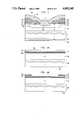
Referring now to FIG. 1, there is shown an n-channelvertical DMOS transistor 10 which is part of a silicon chip whosebulk 12 is of n-type conductivity.Transistor 10 is designed for use as a power transistor. Typically this chip was part of a wafer of much larger surface area in which many like transistors were formed simultaneously. In the interest of simplicity, it is convenient to show the processing of only a single transistor, but it should be understood that normally many such transistors will be formed in a wafer by a common set of steps. Typically the bulk (substrate) 12 of the chip is a moderately low resistivity n-typemonocrystalline silicon substrate 12 on which has been grown epitaxially a higher resistivity n-type layer 14. Within thislayer 14 there is formed a diffused p-type well 16. Well 16 in turn includes on a front surface thereof a relatively low resistivity n+ type annularisland source region 18. A via throughsource region 18 exposes a central portion (region) 24 of thewell 16. The portion of well 16 between vertical outer edges ofregion 18 andlayer 14 defines a p-type annular portion (region) 22 of well 16 between the n+type island region 18 and the n-type layer 14. In operation, the conductivity type ofportion 22 of well 16 is inverted and then serves as an n-type channel which electrically connectsregion 18 tolayer 14.Portion 22 is usually denoted as the channel portion of well 16.Portion 24 of thewell 16, which is not inverted, is usually denoted as the body diode portion of well 16.
Afirst electrode 26 on the front surface of the chip makes direct contact both to the annular n+type source region 18 and to thebody diode portion 24 of well 16. Asecond electrode 28 on the back surface of the chip makes contact to the n-type bulk (substrate)portion 12 of the chip. Generally, to desirably decrease the resistance of the latter contact, the back surface of the chip is doped with n-type dopants to form an n+type surface layer 30 andelectrode 28contacts layer 30.Electrodes
As is characteristic of an MOS transistor, a silicon oxide (typically essentially silicon dioxide)layer 32 overlies portions of the front surface of the chip, including particularly the channel portion (region) 22 of the p-type well 16.
On thisoxide layer 32 and overlying theannular region 22, there is agate electrode 34 which is typically polycrystalline silicon.Gate electrode 34 is generally doped to be heavily n-type, to set a desired threshold voltage for the inversion ofregion 22 to n-type conductivity so as to selectively electrically connectregion 18 tolayer 14. Although not shown in the drawing, the overlying metal layer that forms thesource electrode 26 will be appropriately patterned to permit connection to be made to thegate electrode 34 so that gate voltages may be applied to it.
Aninsulating layer 36, typically of phosphosilicate glass, serves as an insulating layer to isolate thepolysilicon gate electrode 34 from thesource electrode 26. The preparation of such a transistor in accordance with an illustrative embodiment of the invention will now be described with reference to FIGS. 2A through 2H.
Referring now to FIG. 2A, there is shown asilicon wafer 50 of which only a portion adequate to provide a silicon chip including a single transistor is shown. Wafer 50 includes a moderately doped n-type substrate portion 52 (typically about 1018 donors per cubic centimeter) of sufficient thickness (typically about 25 mils) to provide mechanical strength and ruggedness to thewafer 50. An epitaxial layer 54 (typically 1017 microns) of n-type conductivity (typically 1017 donors per cubic centimeter) is grown overwafer 50. Then generally a relatively thick field oxide layer is formed over the wafer, usually by heating in an oxidizing ambient for an appropriate time. This oxide layer is then patterned by photolithographic techniques to remove this thick layer both from a back (bottom)surface 64 of thewafer 50 and from selected front (top)surface regions 63 of thewafer 50 where active devices are to be formed. Since only the portion of thewafer 50 in which a transistor is to be formed is shown in FIG. 2A, the described thick oxide layer is not seen since it has been removed from the shown portion ofsurface region 63 ofwafer 50.
Then anew layer 56 of silicon oxide (typically essentially silicon dioxide), relatively thin to be suitable for use as a gate oxide, is grown over such exposedfront surface 63 of thewafer 50. In an illustrative embodiment, this layer is about 1000 Angstroms thick, as compared to a field oxide layer thickness of about 6000 Angstroms. This is followed by the deposition overlayer 56 of apolycrystalline silicon layer 58 which is initially relatively free of doping and typically is about 4500 Angstroms thick. Any of various known techniques can be employed for such deposition.
Thepolysilicon layer 58 on thefront surface 63 is thereafter masked by a layer of a photoresist 60 which is thereafter patterned photolithographically. Then the exposed polysilicon is etched away to leave thepolysilicon layer 58 correspondingly patterned as shown in FIG. 2B.
Thepolysilicon 58 and its overlyingphotoresist 60 are then used as a mask for the implantation of thewafer 50 with acceptor ions, typically boron at about 100 kiloelectron volts. Next thephotoresist 60 is stripped off thewafer 50, typically either by etching in a sulfuric acid bath or in an oxygen plasma. Thewafer 50 is then heated to drive the implanted boron ions deeper into thewafer 50 to form a moderately doped p-type well 62. The result is shown in FIG. 2C. Typically the well 16 is several microns deep with a surface sheet resistivity of about 600 ohms per square. There then is stripped from theback surface 64 of thewafer 50 any polysilicon and oxide that may have formed there. Alternatively, such stripping may be done before the boron drive-in heating.
The patternedpolysilicon 58 is advantageously also used as a mask to remove the portion of the thinsilicon oxide layer 56 exposed in the polysilicon pattern to arrive at the structure shown in FIG. 2C. It should be noted that the drive-in heating step has extended the edge of the p-type diffusion well 62 laterally so that a portion of the well 62 underlies thepolycrystalline layer 58.
Then in a common predeposition step, a donor, advantageously phosphorus, is introduced over the exposed front surfaces of well 62, thepolysilicon layer 58 and theback surface 64 of thesubstrate 52. This typically involves heating the wafer in a phosphorus-rich ambient to introduce a controlled amount of phosphorus shallowly in such regions. This is then followed by further heating at a higher temperature in a phosphorus-free ambient to drive the shallow phosphorus deposit deeper.
First, this serves to form at the surface of the well 62 a relatively heavily doped n+type source region 66, whose edge just underlies thepolysilicon layer 58 and is separated from it bygate oxide layer 56. Typically this source region is about 0.4 micron deep with a surface sheet resistivity of about 20 ohms per square. However, there remains unconverted anannular surface portion 68 of p-well 62 that underlies thepolysilicon layer 58.Portion 68 ofwell 62 serves as the channel (typically about 1.5 microns wide) of the DMOS between thesource region 66 and thelayer 54 which is part of the drain region. The remainingportion 67 ofwell 62 serves as the body diode. The result is seen in FIG. 2D.
Second, the phosphorus introduction serves to provide n-type conductivity to thepolysilicon layer 58 and better adapts it to serve as the gate electrode of the DMOS.
Third, the phosphorus introduction into theback surface 64 forms there a more heavily doped layer 65 (surface sheet resistivity of about 20 ohms per square).Layer 65 is useful to facilitate the making of a low resistance connection thereto and reduces the need for grinding such back surface before the backside drain electrode 78 (shown in FIG. 2H) is deposited thereover.
Next, as seen in FIG. 2E, there is deposited over thefront surface 63 of thewafer 50 an insulatinglayer 69 which is used to isolate thepolysilicon electrode 58 from the subsequent source electrode metallization (shown in FIG. 2H as electrode 76). The forming oflayer 69 typically involves depositing a phosphosilicate glass at a relatively low temperature followed by heating at a higher temperature to densify the glass. Next, a layer ofphotoresist 70 is deposited over thephosphosilicate glass 69.
Then, as is shown in FIG. 2F, thephotoresist layer 70 is first patterned to form anopening 71A (typically 5 microns wide) in it for use as a mask in patterning thephosphosilicate glass layer 69. Then theglass layer 69 is patterned to provide an opening 71B in thelayer 69. For patterning theglass layer 69, an isotropic wet etchant is used to insure some undercutting of the patternedphotoresist layer 70 to provide for opening 71B which has a width of about 7 microns.
Next, as is shown in FIG. 2G, with the patternedphotoresist layer 70 still in place to act as a shadow mask, thefront face 63 of thewafer 50 is exposed to a gas plasma, typically SF6. This etches substantially anisotropically to form a via 72 (typically about 5 microns wide) through a central portion of thelayer 66 and exposes a central body diode portion of the p-type well 62. Anedge portion 66a of thelayer 66 exposed by the previously mentioned undercutting in the patternedphosphosilicate layer 69 is left in place.
This plasma etch is chosen to provide a via 72 which substantially conforms in area to the area originally defined by the edge of theopening 71A in thephotoresist masking layer 70. It is chosen also to leave sloping curved walls in the via which are less vertical than would result from a more anisotropic reactive ion etch. Such curved sloping in the sidewalls of the via 72 is desirable to permit better filling of the via 72 by the subsequent metallization. A known SF6 plasma is useful to provide such etching.
Advantageously, thewafer 50 is then exposed to a buffered oxide etch for selectively etching theglassy layer 69 and widening its opening to about 9 microns to increase the amount of n-type source region 66 that will contact the source electrode 76 (see FIG. 2H).
Next, as is shown in FIG. 2H, afterphotoresist layer 70 is removed, there is deposited over the front surface aconductive layer 76, typically of aluminum. This fills the via 72 and forms direct contact both to the exposed central portion of the p-type well 62 and to the exposed vertical edge and horizontal edge 66A of the via 72 formed in thesource region 66. Thislayer 76 serves both as the source electrode and as an electrical short between thesource region 66 and a body diode portion ofwell 62.
Themetal layer 76 is then etched in conventional fashion in a desired pattern that includes openings (not shown) to permit contact to be made to thepolysilicon gate electrode 58. Next, one would usually heat thewafer 50 to alloy the remaining aluminum to the silicon, which improves the electrical contact therebetween.
Normally a silicon nitride passivating layer (not shown) would then be provided over the now built upfront surface 63. This layer is then appropriately patterned to expose pads to which leads may be bonded
Then aconductive layer 78 is deposited over the phosphorus-dopedlayer 65 to serve as the drain electrode.Conductive layer 78 is preferably nickel when theconductive layer 78 is to be soldered to a header member that is to be used in an automobile. In other applications other conductors, such as aluminum, can be used aslayer 78. Before such deposit, it has usually been advantageous to grind the back surface to roughen the surface to facilitate making a low resistance connection. However, the earlier phosphorous doping to form heavily dopedlayer 65 at such surface, as described, may eliminate or at least reduce, the amount needed of such grinding. The resultant is shown in FIG. 2H. This structure is the same as that shown in FIG. 1 with different reference numerals.
For the sake of brevity in the forgoing description, there has been omitted mention of the usual cleaning steps normally performed after the etching, implantation, diffusion and deposition steps to remove undesirable by-products of such steps.
Reviewing briefly, a first feature of the preferred embodiment of the invention involves stripping the back surface of the wafer to bare such back surface earlier than was customary in the past. Subsequently, a common phosphorous diffusion operation can be used to form a heavily doped layer on the bared back surface, to dope the polysilicon gate electrode layer, and to form the n-type source region. This permits elimination of at least one mask operation from previous practice.
Additionally, a second feature of the invention is the use of the source region contact mask as a shadow mask in the substantially anisotropic etching of a via through the n-type source region to the underlying body diode region of the underlying p-type well. This permits a later deposited source electrode to also serve as a shorting contact to this body diode region.
It is to be understood that the specific embodiment described is merely illustrative of the general principles involved and that other structures are feasible and still consistent with the spirit and scope of the invention. For example, with the conductivity types of the n-channel DMOS transistor reversed, it becomes a p-channel DMOS transistor. Similarly, specific details, such as the materials used for doping and for the contacts or the dimensions involved, may be different. Moreover, while the order of some of the steps in the process described is critical, the order of others is discretionary, as should be apparent to a skilled worker in the art.
Claims (7)
1. A process for making a semiconductive device comprising the steps of:
preparing a silicon wafer of one conductivity type having opposed front and back surfaces;
forming over the front surface and insulated therefrom a patterned polysilicon layer suitable for use as a silicon gate electrode;
using the polysilicon layer as a mask for forming over the front surface a surface well having a conductivity type opposite said one type;
doping simultaneously with dopant ions of the type characteristic of the one-type a surface portion of said surface well, the polysilicon layer and the back surface of the water, which had been previously stripped of any polysilicon or oxide;
driving in said dopants to form a source region of the one conductivity type at the surface of the well region, leaving unconverted a channel portion and a body diode portion of the well region, and to increase the conductivity of the polysilicon layer and of the back surface; and
providing a source electrode contacting both the source region and the body diode portion and providing a drain electrode contacting the back surface.
2. The process of claim 1 in which the providing of the source electrode includes:
forming an insulating layer over the front surface and the patterned polysilicon layer;
providing a masking layer over said insulating layer;
forming an opening in said masking layer over a central portion of the source region;
etching isotropically the insulating layer through the opening in the masking layer to form an opening in the insulating layer that undercuts the masking layer and exposes a portion of the source region at such opening;
etching substantially anisotropically the exposed portion of the source region to form a via, through the source region to the underlying body diode portion of the well region, whose area essentially corresponds to that of the opening in the masking layer; and
depositing a conductive layer for use as the source electrode that contacts the source region along the side and top edges of the via and the body diode portion of the well region by way of the via.
3. A process for making a vertical DMOS transistor comprising the steps of:
preparing a silicon wafer of one conductivity type with front and back surfaces;
forming on the front surface a silicon oxide gate layer; forming over said silicon oxide layer a patterned polysilicon layer suitable for use as a silicon gate electrode;
forming in a portion of the front surface of the wafer a surface well of the opposite conductivity type using the patterned polysilicon gate as a mask;
stripping the back surface of the wafer and the exposed surface of the well region of the gate oxide layer;
exposing the silicon wafer to an ambient of dopants of the conductivity type predominant in the wafer simultaneously to form a source region of the one conductivity type at the surface of the well region, to dope the polysilicon layer to adapt it for use as the gate electrode, and to open the back surface of the wafer to facilitate the provision thereto of a drain electrode; and
forming source and drain electrodes to the source region and the back surface of the bulk portion, respectively.
4. The process of claim 3 in which the forming of source electrode to the source region includes the steps of:
forming an insulating layer over the front surface;
forming over said insulating layer a masking layer defining an aperture overlying the source region;
etching the insulating layer isotropically through the aperture in the masking layer for forming an opening in the insulating layer larger than said aperture for exposing a portion of the source region;
etching substantially anisotropically the source region for forming a via to the underlying well region of area substantially corresponding to that of the aperture in the masking layer;
stripping away the masking layer; and
depositing a metal layer for use as the source electrode over said insulating layer for filling the opening in the insulating layer, thereby contacting the well region by way of the via in the source region and the source region along the vertical and lateral edges of the via.
5. In a process of making a DMOS transistor that comprises a source electrode that contacts both a central portion of a body diode portion of a well region of one conductivity type and an annular source region of the opposite conductivity type surrounding said central portion, the steps of:
forming, on a first surface of a semiconductive wafer whose bulk is of one conductivity type, a well region of the opposite conductivity type that surrounds an island surface region which is of the one conductivity type and is useful as a source region;
depositing an insulating layer over said first surface;
depositing a masking layer over said insulating layer;
forming an opening in the masking layer overlying a central portion of the island surface region;
etching the insulating layer through the opening in the masking layer in a manner to undercut the masking layer and form an opening in the insulating layer of an area larger than the opening in the masking layer;
etching the wafer through the openings in the masking and insulating layers to form a via through a central portion of said island surface region of an area substantially corresponding to the area of the opening in the masking layer, leaving exposed edge portions of the via;
stripping the masking layer; and
depositing a layer suitable for use as the source electrode over the insulating layer through the opening in the insulating layer and the via in the island surface region to contact both the island surface region at the exposed edges of the via and the underlying body diode portion of the well region through the via in the island surface region.
6. The process of claim 5 in which the etching of the insulating layer through the opening in the masking layer uses an isotropic wet etchant while the etching of the wafer to form a via uses a plasma etch that is substantially anisotropic.
7. The process of claim 6 which includes after the etching of the wafer and before the stripping of the masking layer the step of etching the insulating layer selectively to further expose the island surface region around the periphery of the via.
Priority Applications (1)
| Application Number | Priority Date | Filing Date | Title |
|---|---|---|---|
| US07/234,761US4853345A (en) | 1988-08-22 | 1988-08-22 | Process for manufacture of a vertical DMOS transistor |
Applications Claiming Priority (1)
| Application Number | Priority Date | Filing Date | Title |
|---|---|---|---|
| US07/234,761US4853345A (en) | 1988-08-22 | 1988-08-22 | Process for manufacture of a vertical DMOS transistor |
Publications (1)
| Publication Number | Publication Date |
|---|---|
| US4853345Atrue US4853345A (en) | 1989-08-01 |
Family
ID=22882713
Family Applications (1)
| Application Number | Title | Priority Date | Filing Date |
|---|---|---|---|
| US07/234,761Expired - LifetimeUS4853345A (en) | 1988-08-22 | 1988-08-22 | Process for manufacture of a vertical DMOS transistor |
Country Status (1)
| Country | Link |
|---|---|
| US (1) | US4853345A (en) |
Cited By (63)
| Publication number | Priority date | Publication date | Assignee | Title |
|---|---|---|---|---|
| US5086007A (en)* | 1989-05-24 | 1992-02-04 | Fuji Electric Co., Ltd. | Method of manufacturing an insulated gate field effect transistor |
| US5182222A (en)* | 1991-06-26 | 1993-01-26 | Texas Instruments Incorporated | Process for manufacturing a DMOS transistor |
| US5414283A (en)* | 1993-11-19 | 1995-05-09 | Ois Optical Imaging Systems, Inc. | TFT with reduced parasitic capacitance |
| WO1996007200A1 (en)* | 1994-09-01 | 1996-03-07 | International Rectifier Corporation | Process for manufacture of mos gated device with reduced mask count |
| US5498570A (en)* | 1994-09-15 | 1996-03-12 | Micron Technology Inc. | Method of reducing overetch during the formation of a semiconductor device |
| US5545915A (en)* | 1995-01-23 | 1996-08-13 | Delco Electronics Corporation | Semiconductor device having field limiting ring and a process therefor |
| US5684319A (en)* | 1995-08-24 | 1997-11-04 | National Semiconductor Corporation | Self-aligned source and body contact structure for high performance DMOS transistors and method of fabricating same |
| US5689130A (en)* | 1990-02-14 | 1997-11-18 | Nippondenso Co., Ltd. | Vertical semiconductor device with ground surface providing a reduced ON resistance |
| EP0704894A3 (en)* | 1994-09-23 | 1997-11-26 | Siemens Aktiengesellschaft | Process for forming a low ohmic contact between a metallic layer and a semiconductor material |
| US5716873A (en)* | 1996-05-06 | 1998-02-10 | Micro Technology, Inc. | Method for cleaning waste matter from the backside of a semiconductor wafer substrate |
| US5843796A (en)* | 1995-09-11 | 1998-12-01 | Delco Electronics Corporation | Method of making an insulated gate bipolar transistor with high-energy P+ im |
| EP0766318A4 (en)* | 1995-04-11 | 1999-01-13 | Rohm Co Ltd | SEMICONDUCTOR HAVING VERTICAL PLANAR DEVICES WITH HIGH HOLDING VOLTAGE AND METHOD FOR PRODUCING SAID SEMICONDUCTOR |
| US5879994A (en)* | 1997-04-15 | 1999-03-09 | National Semiconductor Corporation | Self-aligned method of fabricating terrace gate DMOS transistor |
| EP0889511A3 (en)* | 1997-06-30 | 1999-03-31 | Harris Corporation | Trench contact process |
| US6037628A (en)* | 1997-06-30 | 2000-03-14 | Intersil Corporation | Semiconductor structures with trench contacts |
| US6051501A (en)* | 1996-10-09 | 2000-04-18 | Micron Technology, Inc. | Method of reducing overetch during the formation of a semiconductor device |
| US6100150A (en)* | 1998-09-04 | 2000-08-08 | Taiwan Semiconductor Manufacturing Company | Process to improve temperature uniformity during RTA by deposition of in situ poly on the wafer backside |
| US6153501A (en)* | 1998-05-19 | 2000-11-28 | Micron Technology, Inc. | Method of reducing overetch during the formation of a semiconductor device |
| US6153473A (en)* | 1997-12-12 | 2000-11-28 | National Semiconductor Corporation | Method of symmetrically implanted punch-through stopper for a rugged DMOS power device |
| US20030060013A1 (en)* | 1999-09-24 | 2003-03-27 | Bruce D. Marchant | Method of manufacturing trench field effect transistors with trenched heavy body |
| US6660592B2 (en)* | 2001-11-21 | 2003-12-09 | Mosel Vitelic, Inc. | Fabricating a DMOS transistor |
| US6710418B1 (en) | 2002-10-11 | 2004-03-23 | Fairchild Semiconductor Corporation | Schottky rectifier with insulation-filled trenches and method of forming the same |
| US6710403B2 (en) | 2002-07-30 | 2004-03-23 | Fairchild Semiconductor Corporation | Dual trench power MOSFET |
| US6803626B2 (en) | 2002-07-18 | 2004-10-12 | Fairchild Semiconductor Corporation | Vertical charge control semiconductor device |
| US6916745B2 (en) | 2003-05-20 | 2005-07-12 | Fairchild Semiconductor Corporation | Structure and method for forming a trench MOSFET having self-aligned features |
| WO2005027198A3 (en)* | 2003-09-08 | 2005-09-22 | Honeywell Int Inc | Doped alloys for electrical interconnects, methods of production and uses thereof |
| US6991977B2 (en) | 2001-10-17 | 2006-01-31 | Fairchild Semiconductor Corporation | Method for forming a semiconductor structure with improved smaller forward voltage loss and higher blocking capability |
| US7033891B2 (en) | 2002-10-03 | 2006-04-25 | Fairchild Semiconductor Corporation | Trench gate laterally diffused MOSFET devices and methods for making such devices |
| US20060113683A1 (en)* | 2004-09-07 | 2006-06-01 | Nancy Dean | Doped alloys for electrical interconnects, methods of production and uses thereof |
| US7061066B2 (en) | 2001-10-17 | 2006-06-13 | Fairchild Semiconductor Corporation | Schottky diode using charge balance structure |
| US20060141763A1 (en)* | 2004-12-23 | 2006-06-29 | Advantech Global, Ltd | System for and method of planarizing the contact region of a via by use of a continuous inline vacuum deposition |
| US20060141761A1 (en)* | 2004-12-23 | 2006-06-29 | Advantech Global, Ltd | System for and method of forming via holes by multiple deposition events in a continuous inline shadow mask deposition process |
| US20060148241A1 (en)* | 2004-12-30 | 2006-07-06 | Advantech Global, Ltd | System for and method of forming via holes by use of selective plasma etching in a continuous inline shadow mask deposition process |
| US7078296B2 (en) | 2002-01-16 | 2006-07-18 | Fairchild Semiconductor Corporation | Self-aligned trench MOSFETs and methods for making the same |
| US7132712B2 (en) | 2002-11-05 | 2006-11-07 | Fairchild Semiconductor Corporation | Trench structure having one or more diodes embedded therein adjacent a PN junction |
| US7265416B2 (en) | 2002-02-23 | 2007-09-04 | Fairchild Korea Semiconductor Ltd. | High breakdown voltage low on-resistance lateral DMOS transistor |
| US7265415B2 (en) | 2004-10-08 | 2007-09-04 | Fairchild Semiconductor Corporation | MOS-gated transistor with reduced miller capacitance |
| US7301203B2 (en) | 2003-11-28 | 2007-11-27 | Fairchild Korea Semiconductor Ltd. | Superjunction semiconductor device |
| US7319256B1 (en) | 2006-06-19 | 2008-01-15 | Fairchild Semiconductor Corporation | Shielded gate trench FET with the shield and gate electrodes being connected together |
| US7345342B2 (en) | 2001-01-30 | 2008-03-18 | Fairchild Semiconductor Corporation | Power semiconductor devices and methods of manufacture |
| US7352036B2 (en) | 2004-08-03 | 2008-04-01 | Fairchild Semiconductor Corporation | Semiconductor power device having a top-side drain using a sinker trench |
| US7368777B2 (en) | 2003-12-30 | 2008-05-06 | Fairchild Semiconductor Corporation | Accumulation device with charge balance structure and method of forming the same |
| US7385248B2 (en) | 2005-08-09 | 2008-06-10 | Fairchild Semiconductor Corporation | Shielded gate field effect transistor with improved inter-poly dielectric |
| US7446374B2 (en) | 2006-03-24 | 2008-11-04 | Fairchild Semiconductor Corporation | High density trench FET with integrated Schottky diode and method of manufacture |
| US7504306B2 (en) | 2005-04-06 | 2009-03-17 | Fairchild Semiconductor Corporation | Method of forming trench gate field effect transistor with recessed mesas |
| US7576388B1 (en) | 2002-10-03 | 2009-08-18 | Fairchild Semiconductor Corporation | Trench-gate LDMOS structures |
| US7625793B2 (en) | 1999-12-20 | 2009-12-01 | Fairchild Semiconductor Corporation | Power MOS device with improved gate charge performance |
| US7638841B2 (en) | 2003-05-20 | 2009-12-29 | Fairchild Semiconductor Corporation | Power semiconductor devices and methods of manufacture |
| US7745289B2 (en) | 2000-08-16 | 2010-06-29 | Fairchild Semiconductor Corporation | Method of forming a FET having ultra-low on-resistance and low gate charge |
| US7772668B2 (en) | 2007-12-26 | 2010-08-10 | Fairchild Semiconductor Corporation | Shielded gate trench FET with multiple channels |
| US8319290B2 (en) | 2010-06-18 | 2012-11-27 | Fairchild Semiconductor Corporation | Trench MOS barrier schottky rectifier with a planar surface using CMP techniques |
| US8673700B2 (en) | 2011-04-27 | 2014-03-18 | Fairchild Semiconductor Corporation | Superjunction structures for power devices and methods of manufacture |
| US20140159144A1 (en)* | 2012-12-12 | 2014-06-12 | Beyond Innovation Technology Co., Ltd. | Trench gate mosfet and method of forming the same |
| US8772868B2 (en) | 2011-04-27 | 2014-07-08 | Fairchild Semiconductor Corporation | Superjunction structures for power devices and methods of manufacture |
| US8786010B2 (en) | 2011-04-27 | 2014-07-22 | Fairchild Semiconductor Corporation | Superjunction structures for power devices and methods of manufacture |
| US8829641B2 (en) | 2001-01-30 | 2014-09-09 | Fairchild Semiconductor Corporation | Method of forming a dual-trench field effect transistor |
| US8836028B2 (en) | 2011-04-27 | 2014-09-16 | Fairchild Semiconductor Corporation | Superjunction structures for power devices and methods of manufacture |
| US8928077B2 (en) | 2007-09-21 | 2015-01-06 | Fairchild Semiconductor Corporation | Superjunction structures for power devices |
| US8963212B2 (en) | 2008-12-08 | 2015-02-24 | Fairchild Semiconductor Corporation | Trench-based power semiconductor devices with increased breakdown voltage characteristics |
| US9431481B2 (en) | 2008-09-19 | 2016-08-30 | Fairchild Semiconductor Corporation | Superjunction structures for power devices and methods of manufacture |
| US20160307995A1 (en)* | 2013-08-27 | 2016-10-20 | Csmc Technologies Fab1 Co., Ltd. | Insulated gate bipolar transistor and manufacturing method therefor |
| US20210328026A1 (en)* | 2018-07-12 | 2021-10-21 | Flosfia Inc. | Layered structure, semiconductor device including layered structure, and semiconductor system |
| US20240096981A1 (en)* | 2022-09-15 | 2024-03-21 | National Yang Ming Chiao Tung University | Three-dimensional source contact structure and fabrication process method of making the same |
Citations (10)
| Publication number | Priority date | Publication date | Assignee | Title |
|---|---|---|---|---|
| US4372034A (en)* | 1981-03-26 | 1983-02-08 | Intel Corporation | Process for forming contact openings through oxide layers |
| US4443931A (en)* | 1982-06-28 | 1984-04-24 | General Electric Company | Method of fabricating a semiconductor device with a base region having a deep portion |
| US4502069A (en)* | 1980-04-30 | 1985-02-26 | Siemens Aktiengesellschaft | Contact for an MIS-semiconductor component and method for manufacturing the same |
| US4503598A (en)* | 1982-05-20 | 1985-03-12 | Fairchild Camera & Instrument Corporation | Method of fabricating power MOSFET structure utilizing self-aligned diffusion and etching techniques |
| US4516143A (en)* | 1982-01-04 | 1985-05-07 | General Electric Company | Self-aligned power MOSFET with integral source-base short and methods of making |
| US4561168A (en)* | 1982-11-22 | 1985-12-31 | Siliconix Incorporated | Method of making shadow isolated metal DMOS FET device |
| US4716126A (en)* | 1986-06-05 | 1987-12-29 | Siliconix Incorporated | Fabrication of double diffused metal oxide semiconductor transistor |
| US4774198A (en)* | 1986-03-06 | 1988-09-27 | Sgs Microelettronica Spa | Self-aligned process for fabricating small DMOS cells |
| US4785344A (en)* | 1984-01-27 | 1988-11-15 | Siemens Aktiengesellschaft | Semi-conductor component with contact hole |
| US4798810A (en)* | 1986-03-10 | 1989-01-17 | Siliconix Incorporated | Method for manufacturing a power MOS transistor |
- 1988
- 1988-08-22USUS07/234,761patent/US4853345A/ennot_activeExpired - Lifetime
Patent Citations (11)
| Publication number | Priority date | Publication date | Assignee | Title |
|---|---|---|---|---|
| US4502069A (en)* | 1980-04-30 | 1985-02-26 | Siemens Aktiengesellschaft | Contact for an MIS-semiconductor component and method for manufacturing the same |
| US4372034A (en)* | 1981-03-26 | 1983-02-08 | Intel Corporation | Process for forming contact openings through oxide layers |
| US4372034B1 (en)* | 1981-03-26 | 1998-07-21 | Intel Corp | Process for forming contact openings through oxide layers |
| US4516143A (en)* | 1982-01-04 | 1985-05-07 | General Electric Company | Self-aligned power MOSFET with integral source-base short and methods of making |
| US4503598A (en)* | 1982-05-20 | 1985-03-12 | Fairchild Camera & Instrument Corporation | Method of fabricating power MOSFET structure utilizing self-aligned diffusion and etching techniques |
| US4443931A (en)* | 1982-06-28 | 1984-04-24 | General Electric Company | Method of fabricating a semiconductor device with a base region having a deep portion |
| US4561168A (en)* | 1982-11-22 | 1985-12-31 | Siliconix Incorporated | Method of making shadow isolated metal DMOS FET device |
| US4785344A (en)* | 1984-01-27 | 1988-11-15 | Siemens Aktiengesellschaft | Semi-conductor component with contact hole |
| US4774198A (en)* | 1986-03-06 | 1988-09-27 | Sgs Microelettronica Spa | Self-aligned process for fabricating small DMOS cells |
| US4798810A (en)* | 1986-03-10 | 1989-01-17 | Siliconix Incorporated | Method for manufacturing a power MOS transistor |
| US4716126A (en)* | 1986-06-05 | 1987-12-29 | Siliconix Incorporated | Fabrication of double diffused metal oxide semiconductor transistor |
Non-Patent Citations (2)
| Title |
|---|
| G. Bell and W. Ladenhauf, "SIPMOS Technology, an Example of VLSI Precision Realized with Standard LSI for Power Transistors," Siemens Forsch.-u. Entwickl.-Ber. Bd. 9(1980), Nr. 4, Springer-Verlag 1980. |
| G. Bell and W. Ladenhauf, SIPMOS Technology, an Example of VLSI Precision Realized with Standard LSI for Power Transistors, Siemens Forsch. u. Entwickl. Ber. Bd. 9(1980), Nr. 4, Springer Verlag 1980.* |
Cited By (136)
| Publication number | Priority date | Publication date | Assignee | Title |
|---|---|---|---|---|
| US5086007A (en)* | 1989-05-24 | 1992-02-04 | Fuji Electric Co., Ltd. | Method of manufacturing an insulated gate field effect transistor |
| US6649478B2 (en) | 1990-02-14 | 2003-11-18 | Denso Corporation | Semiconductor device and method of manufacturing same |
| US20040036140A1 (en)* | 1990-02-14 | 2004-02-26 | Yoshifumi Okabe | Semiconductor device and method of manufacturing same |
| US20040241930A1 (en)* | 1990-02-14 | 2004-12-02 | Yoshifumi Okabe | Semiconductor device and method of manufacturing same |
| US20040237327A1 (en)* | 1990-02-14 | 2004-12-02 | Yoshifumi Okabe | Semiconductor device and method of manufacturing same |
| US5994187A (en)* | 1990-02-14 | 1999-11-30 | Nippondenso Co., Ltd. | Method of manufacturing a vertical semiconductor device |
| US6903417B2 (en) | 1990-02-14 | 2005-06-07 | Denso Corporation | Power semiconductor device |
| US6949434B2 (en) | 1990-02-14 | 2005-09-27 | Denso Corporation | Method of manufacturing a vertical semiconductor device |
| US5689130A (en)* | 1990-02-14 | 1997-11-18 | Nippondenso Co., Ltd. | Vertical semiconductor device with ground surface providing a reduced ON resistance |
| US7064033B2 (en) | 1990-02-14 | 2006-06-20 | Denso Corporation | Semiconductor device and method of manufacturing same |
| US5182222A (en)* | 1991-06-26 | 1993-01-26 | Texas Instruments Incorporated | Process for manufacturing a DMOS transistor |
| US5614427A (en)* | 1993-11-19 | 1997-03-25 | Ois Optical Imaging Systems, Inc. | Method of making an array of TFTs having reduced parasitic capacitance |
| US5414283A (en)* | 1993-11-19 | 1995-05-09 | Ois Optical Imaging Systems, Inc. | TFT with reduced parasitic capacitance |
| US5795793A (en)* | 1994-09-01 | 1998-08-18 | International Rectifier Corporation | Process for manufacture of MOS gated device with reduced mask count |
| EP0777910A4 (en)* | 1994-09-01 | 1998-10-07 | Int Rectifier Corp | METHOD FOR PRODUCING A MOS-CONTROLLED COMPONENT WITH A REDUCED MASK NUMBER |
| EP1686616A3 (en)* | 1994-09-01 | 2009-03-18 | International Rectifier Corporation | Process for manufacture of mos gated device with reduced mask count |
| WO1996007200A1 (en)* | 1994-09-01 | 1996-03-07 | International Rectifier Corporation | Process for manufacture of mos gated device with reduced mask count |
| JP3416617B2 (en) | 1994-09-01 | 2003-06-16 | インターナショナル・レクチファイヤー・コーポレーション | Manufacturing process of MOS gate device with reduced number of masks |
| US6759320B2 (en) | 1994-09-15 | 2004-07-06 | Micron Technology, Inc. | Method of reducing overetch during the formation of a semiconductor device |
| US6451678B1 (en) | 1994-09-15 | 2002-09-17 | Micron Technology, Lnc. | Method of reducing overetch during the formation of a semiconductor device |
| US5753565A (en)* | 1994-09-15 | 1998-05-19 | Micron Technology, Inc. | Method of reducing overetch during the formation of a semiconductor device |
| US5498570A (en)* | 1994-09-15 | 1996-03-12 | Micron Technology Inc. | Method of reducing overetch during the formation of a semiconductor device |
| EP0704894A3 (en)* | 1994-09-23 | 1997-11-26 | Siemens Aktiengesellschaft | Process for forming a low ohmic contact between a metallic layer and a semiconductor material |
| US5545915A (en)* | 1995-01-23 | 1996-08-13 | Delco Electronics Corporation | Semiconductor device having field limiting ring and a process therefor |
| US5672528A (en)* | 1995-01-23 | 1997-09-30 | Delco Electronics Corporation | Method for making semiconductor device having field limiting ring |
| EP0766318A4 (en)* | 1995-04-11 | 1999-01-13 | Rohm Co Ltd | SEMICONDUCTOR HAVING VERTICAL PLANAR DEVICES WITH HIGH HOLDING VOLTAGE AND METHOD FOR PRODUCING SAID SEMICONDUCTOR |
| US5684319A (en)* | 1995-08-24 | 1997-11-04 | National Semiconductor Corporation | Self-aligned source and body contact structure for high performance DMOS transistors and method of fabricating same |
| US5843796A (en)* | 1995-09-11 | 1998-12-01 | Delco Electronics Corporation | Method of making an insulated gate bipolar transistor with high-energy P+ im |
| US5910668A (en)* | 1995-09-11 | 1999-06-08 | Delco Electronics Corporation | Method of making a insulated gate bipolar transistor with high-energy P+ implant and silicon-etch contact |
| US5716873A (en)* | 1996-05-06 | 1998-02-10 | Micro Technology, Inc. | Method for cleaning waste matter from the backside of a semiconductor wafer substrate |
| US6051501A (en)* | 1996-10-09 | 2000-04-18 | Micron Technology, Inc. | Method of reducing overetch during the formation of a semiconductor device |
| US5879994A (en)* | 1997-04-15 | 1999-03-09 | National Semiconductor Corporation | Self-aligned method of fabricating terrace gate DMOS transistor |
| EP0889511A3 (en)* | 1997-06-30 | 1999-03-31 | Harris Corporation | Trench contact process |
| US6630711B2 (en) | 1997-06-30 | 2003-10-07 | Fairchild Semiconductor Corporation | Semiconductor structures with trench contacts |
| US6037628A (en)* | 1997-06-30 | 2000-03-14 | Intersil Corporation | Semiconductor structures with trench contacts |
| US6153473A (en)* | 1997-12-12 | 2000-11-28 | National Semiconductor Corporation | Method of symmetrically implanted punch-through stopper for a rugged DMOS power device |
| US6153501A (en)* | 1998-05-19 | 2000-11-28 | Micron Technology, Inc. | Method of reducing overetch during the formation of a semiconductor device |
| US6100150A (en)* | 1998-09-04 | 2000-08-08 | Taiwan Semiconductor Manufacturing Company | Process to improve temperature uniformity during RTA by deposition of in situ poly on the wafer backside |
| US20030060013A1 (en)* | 1999-09-24 | 2003-03-27 | Bruce D. Marchant | Method of manufacturing trench field effect transistors with trenched heavy body |
| US7625793B2 (en) | 1999-12-20 | 2009-12-01 | Fairchild Semiconductor Corporation | Power MOS device with improved gate charge performance |
| US7745289B2 (en) | 2000-08-16 | 2010-06-29 | Fairchild Semiconductor Corporation | Method of forming a FET having ultra-low on-resistance and low gate charge |
| US8710584B2 (en) | 2000-08-16 | 2014-04-29 | Fairchild Semiconductor Corporation | FET device having ultra-low on-resistance and low gate charge |
| US8101484B2 (en) | 2000-08-16 | 2012-01-24 | Fairchild Semiconductor Corporation | Method of forming a FET having ultra-low on-resistance and low gate charge |
| US8829641B2 (en) | 2001-01-30 | 2014-09-09 | Fairchild Semiconductor Corporation | Method of forming a dual-trench field effect transistor |
| US9368587B2 (en) | 2001-01-30 | 2016-06-14 | Fairchild Semiconductor Corporation | Accumulation-mode field effect transistor with improved current capability |
| US7345342B2 (en) | 2001-01-30 | 2008-03-18 | Fairchild Semiconductor Corporation | Power semiconductor devices and methods of manufacture |
| US6991977B2 (en) | 2001-10-17 | 2006-01-31 | Fairchild Semiconductor Corporation | Method for forming a semiconductor structure with improved smaller forward voltage loss and higher blocking capability |
| US7061066B2 (en) | 2001-10-17 | 2006-06-13 | Fairchild Semiconductor Corporation | Schottky diode using charge balance structure |
| US20060166473A1 (en)* | 2001-10-17 | 2006-07-27 | Kocon Christopher B | Method of forming schottky diode with charge balance structure |
| US7429523B2 (en) | 2001-10-17 | 2008-09-30 | Fairchild Semiconductor Corporation | Method of forming schottky diode with charge balance structure |
| US6660592B2 (en)* | 2001-11-21 | 2003-12-09 | Mosel Vitelic, Inc. | Fabricating a DMOS transistor |
| US7078296B2 (en) | 2002-01-16 | 2006-07-18 | Fairchild Semiconductor Corporation | Self-aligned trench MOSFETs and methods for making the same |
| US7265416B2 (en) | 2002-02-23 | 2007-09-04 | Fairchild Korea Semiconductor Ltd. | High breakdown voltage low on-resistance lateral DMOS transistor |
| US7605040B2 (en) | 2002-02-23 | 2009-10-20 | Fairchild Korea Semiconductor Ltd. | Method of forming high breakdown voltage low on-resistance lateral DMOS transistor |
| US7977744B2 (en) | 2002-07-18 | 2011-07-12 | Fairchild Semiconductor Corporation | Field effect transistor with trench filled with insulating material and strips of semi-insulating material along trench sidewalls |
| US7291894B2 (en) | 2002-07-18 | 2007-11-06 | Fairchild Semiconductor Corporation | Vertical charge control semiconductor device with low output capacitance |
| US6803626B2 (en) | 2002-07-18 | 2004-10-12 | Fairchild Semiconductor Corporation | Vertical charge control semiconductor device |
| US6710403B2 (en) | 2002-07-30 | 2004-03-23 | Fairchild Semiconductor Corporation | Dual trench power MOSFET |
| US8198677B2 (en) | 2002-10-03 | 2012-06-12 | Fairchild Semiconductor Corporation | Trench-gate LDMOS structures |
| US7576388B1 (en) | 2002-10-03 | 2009-08-18 | Fairchild Semiconductor Corporation | Trench-gate LDMOS structures |
| US7033891B2 (en) | 2002-10-03 | 2006-04-25 | Fairchild Semiconductor Corporation | Trench gate laterally diffused MOSFET devices and methods for making such devices |
| US6710418B1 (en) | 2002-10-11 | 2004-03-23 | Fairchild Semiconductor Corporation | Schottky rectifier with insulation-filled trenches and method of forming the same |
| US7132712B2 (en) | 2002-11-05 | 2006-11-07 | Fairchild Semiconductor Corporation | Trench structure having one or more diodes embedded therein adjacent a PN junction |
| US7582519B2 (en) | 2002-11-05 | 2009-09-01 | Fairchild Semiconductor Corporation | Method of forming a trench structure having one or more diodes embedded therein adjacent a PN junction |
| US8129245B2 (en) | 2003-05-20 | 2012-03-06 | Fairchild Semiconductor Corporation | Methods of manufacturing power semiconductor devices with shield and gate contacts |
| US7855415B2 (en) | 2003-05-20 | 2010-12-21 | Fairchild Semiconductor Corporation | Power semiconductor devices having termination structures and methods of manufacture |
| US8143124B2 (en) | 2003-05-20 | 2012-03-27 | Fairchild Semiconductor Corporation | Methods of making power semiconductor devices with thick bottom oxide layer |
| US8034682B2 (en) | 2003-05-20 | 2011-10-11 | Fairchild Semiconductor Corporation | Power device with trenches having wider upper portion than lower portion |
| US6916745B2 (en) | 2003-05-20 | 2005-07-12 | Fairchild Semiconductor Corporation | Structure and method for forming a trench MOSFET having self-aligned features |
| US8013387B2 (en) | 2003-05-20 | 2011-09-06 | Fairchild Semiconductor Corporation | Power semiconductor devices with shield and gate contacts and methods of manufacture |
| US7344943B2 (en) | 2003-05-20 | 2008-03-18 | Fairchild Semiconductor Corporation | Method for forming a trench MOSFET having self-aligned features |
| US8936985B2 (en) | 2003-05-20 | 2015-01-20 | Fairchild Semiconductor Corporation | Methods related to power semiconductor devices with thick bottom oxide layers |
| US8889511B2 (en) | 2003-05-20 | 2014-11-18 | Fairchild Semiconductor Corporation | Methods of manufacturing power semiconductor devices with trenched shielded split gate transistor |
| US8013391B2 (en) | 2003-05-20 | 2011-09-06 | Fairchild Semiconductor Corporation | Power semiconductor devices with trenched shielded split gate transistor and methods of manufacture |
| US8786045B2 (en) | 2003-05-20 | 2014-07-22 | Fairchild Semiconductor Corporation | Power semiconductor devices having termination structures |
| US8716783B2 (en) | 2003-05-20 | 2014-05-06 | Fairchild Semiconductor Corporation | Power device with self-aligned source regions |
| US7982265B2 (en) | 2003-05-20 | 2011-07-19 | Fairchild Semiconductor Corporation | Trenched shield gate power semiconductor devices and methods of manufacture |
| US8143123B2 (en) | 2003-05-20 | 2012-03-27 | Fairchild Semiconductor Corporation | Methods of forming inter-poly dielectric (IPD) layers in power semiconductor devices |
| US7799636B2 (en) | 2003-05-20 | 2010-09-21 | Fairchild Semiconductor Corporation | Power device with trenches having wider upper portion than lower portion |
| US7652326B2 (en) | 2003-05-20 | 2010-01-26 | Fairchild Semiconductor Corporation | Power semiconductor devices and methods of manufacture |
| US7595524B2 (en) | 2003-05-20 | 2009-09-29 | Fairchild Semiconductor Corporation | Power device with trenches having wider upper portion than lower portion |
| US8350317B2 (en) | 2003-05-20 | 2013-01-08 | Fairchild Semiconductor Corporation | Power semiconductor devices and methods of manufacture |
| US7638841B2 (en) | 2003-05-20 | 2009-12-29 | Fairchild Semiconductor Corporation | Power semiconductor devices and methods of manufacture |
| WO2005027198A3 (en)* | 2003-09-08 | 2005-09-22 | Honeywell Int Inc | Doped alloys for electrical interconnects, methods of production and uses thereof |
| US7655981B2 (en) | 2003-11-28 | 2010-02-02 | Fairchild Korea Semiconductor Ltd. | Superjunction semiconductor device |
| US7301203B2 (en) | 2003-11-28 | 2007-11-27 | Fairchild Korea Semiconductor Ltd. | Superjunction semiconductor device |
| US7368777B2 (en) | 2003-12-30 | 2008-05-06 | Fairchild Semiconductor Corporation | Accumulation device with charge balance structure and method of forming the same |
| US8518777B2 (en) | 2003-12-30 | 2013-08-27 | Fairchild Semiconductor Corporation | Method for forming accumulation-mode field effect transistor with improved current capability |
| US7936008B2 (en) | 2003-12-30 | 2011-05-03 | Fairchild Semiconductor Corporation | Structure and method for forming accumulation-mode field effect transistor with improved current capability |
| US7352036B2 (en) | 2004-08-03 | 2008-04-01 | Fairchild Semiconductor Corporation | Semiconductor power device having a top-side drain using a sinker trench |
| US7732876B2 (en) | 2004-08-03 | 2010-06-08 | Fairchild Semiconductor Corporation | Power transistor with trench sinker for contacting the backside |
| US8148233B2 (en) | 2004-08-03 | 2012-04-03 | Fairchild Semiconductor Corporation | Semiconductor power device having a top-side drain using a sinker trench |
| US8026558B2 (en) | 2004-08-03 | 2011-09-27 | Fairchild Semiconductor Corporation | Semiconductor power device having a top-side drain using a sinker trench |
| US20060113683A1 (en)* | 2004-09-07 | 2006-06-01 | Nancy Dean | Doped alloys for electrical interconnects, methods of production and uses thereof |
| US7534683B2 (en) | 2004-10-08 | 2009-05-19 | Fairchild Semiconductor Corporation | Method of making a MOS-gated transistor with reduced miller capacitance |
| US7265415B2 (en) | 2004-10-08 | 2007-09-04 | Fairchild Semiconductor Corporation | MOS-gated transistor with reduced miller capacitance |
| US20060141763A1 (en)* | 2004-12-23 | 2006-06-29 | Advantech Global, Ltd | System for and method of planarizing the contact region of a via by use of a continuous inline vacuum deposition |
| US7132361B2 (en) | 2004-12-23 | 2006-11-07 | Advantech Global, Ltd | System for and method of forming via holes by multiple deposition events in a continuous inline shadow mask deposition process |
| US20080190659A1 (en)* | 2004-12-23 | 2008-08-14 | Advantech Global, Ltd | System For And Method Of Planarizing The Contact Region Of A Via By Use Of A Continuous Inline Vacuum Deposition Process |
| US20060141761A1 (en)* | 2004-12-23 | 2006-06-29 | Advantech Global, Ltd | System for and method of forming via holes by multiple deposition events in a continuous inline shadow mask deposition process |
| US20070051311A1 (en)* | 2004-12-23 | 2007-03-08 | Advantech Global, Ltd | System for and method of forming via holes by multiple deposition events in a continuous inline shadow mask deposition process |
| US7361585B2 (en) | 2004-12-23 | 2008-04-22 | Advantech Global, Ltd | System for and method of planarizing the contact region of a via by use of a continuous inline vacuum deposition |
| WO2006073818A3 (en)* | 2004-12-30 | 2007-06-21 | Advantech Global Ltd | System for and method of forming via holes by use of selective plasma etching in a continuous inline shadow mask deposition process |
| US7268431B2 (en) | 2004-12-30 | 2007-09-11 | Advantech Global, Ltd | System for and method of forming via holes by use of selective plasma etching in a continuous inline shadow mask deposition process |
| US20060148241A1 (en)* | 2004-12-30 | 2006-07-06 | Advantech Global, Ltd | System for and method of forming via holes by use of selective plasma etching in a continuous inline shadow mask deposition process |
| US8084327B2 (en) | 2005-04-06 | 2011-12-27 | Fairchild Semiconductor Corporation | Method for forming trench gate field effect transistor with recessed mesas using spacers |
| US7504306B2 (en) | 2005-04-06 | 2009-03-17 | Fairchild Semiconductor Corporation | Method of forming trench gate field effect transistor with recessed mesas |
| US8680611B2 (en) | 2005-04-06 | 2014-03-25 | Fairchild Semiconductor Corporation | Field effect transistor and schottky diode structures |
| US7385248B2 (en) | 2005-08-09 | 2008-06-10 | Fairchild Semiconductor Corporation | Shielded gate field effect transistor with improved inter-poly dielectric |
| US7598144B2 (en) | 2005-08-09 | 2009-10-06 | Fairchild Semiconductor Corporation | Method for forming inter-poly dielectric in shielded gate field effect transistor |
| US7446374B2 (en) | 2006-03-24 | 2008-11-04 | Fairchild Semiconductor Corporation | High density trench FET with integrated Schottky diode and method of manufacture |
| US7713822B2 (en) | 2006-03-24 | 2010-05-11 | Fairchild Semiconductor Corporation | Method of forming high density trench FET with integrated Schottky diode |
| US20090035900A1 (en)* | 2006-03-24 | 2009-02-05 | Paul Thorup | Method of Forming High Density Trench FET with Integrated Schottky Diode |
| US20090057754A1 (en)* | 2006-06-19 | 2009-03-05 | Nathan Kraft | Shielded Gate Trench FET with the Shield and Gate Electrodes Connected Together in Non-active Region |
| US7859047B2 (en) | 2006-06-19 | 2010-12-28 | Fairchild Semiconductor Corporation | Shielded gate trench FET with the shield and gate electrodes connected together in non-active region |
| US7319256B1 (en) | 2006-06-19 | 2008-01-15 | Fairchild Semiconductor Corporation | Shielded gate trench FET with the shield and gate electrodes being connected together |
| US7473603B2 (en) | 2006-06-19 | 2009-01-06 | Fairchild Semiconductor Corporation | Method for forming a shielded gate trench FET with the shield and gate electrodes being connected together |
| US9595596B2 (en) | 2007-09-21 | 2017-03-14 | Fairchild Semiconductor Corporation | Superjunction structures for power devices |
| US8928077B2 (en) | 2007-09-21 | 2015-01-06 | Fairchild Semiconductor Corporation | Superjunction structures for power devices |
| US7772668B2 (en) | 2007-12-26 | 2010-08-10 | Fairchild Semiconductor Corporation | Shielded gate trench FET with multiple channels |
| US9224853B2 (en) | 2007-12-26 | 2015-12-29 | Fairchild Semiconductor Corporation | Shielded gate trench FET with multiple channels |
| US9431481B2 (en) | 2008-09-19 | 2016-08-30 | Fairchild Semiconductor Corporation | Superjunction structures for power devices and methods of manufacture |
| US9391193B2 (en) | 2008-12-08 | 2016-07-12 | Fairchild Semiconductor Corporation | Trench-based power semiconductor devices with increased breakdown voltage characteristics |
| US8963212B2 (en) | 2008-12-08 | 2015-02-24 | Fairchild Semiconductor Corporation | Trench-based power semiconductor devices with increased breakdown voltage characteristics |
| US8432000B2 (en) | 2010-06-18 | 2013-04-30 | Fairchild Semiconductor Corporation | Trench MOS barrier schottky rectifier with a planar surface using CMP techniques |
| US8319290B2 (en) | 2010-06-18 | 2012-11-27 | Fairchild Semiconductor Corporation | Trench MOS barrier schottky rectifier with a planar surface using CMP techniques |
| US8673700B2 (en) | 2011-04-27 | 2014-03-18 | Fairchild Semiconductor Corporation | Superjunction structures for power devices and methods of manufacture |
| US8786010B2 (en) | 2011-04-27 | 2014-07-22 | Fairchild Semiconductor Corporation | Superjunction structures for power devices and methods of manufacture |
| US8772868B2 (en) | 2011-04-27 | 2014-07-08 | Fairchild Semiconductor Corporation | Superjunction structures for power devices and methods of manufacture |
| US8836028B2 (en) | 2011-04-27 | 2014-09-16 | Fairchild Semiconductor Corporation | Superjunction structures for power devices and methods of manufacture |
| US20140159144A1 (en)* | 2012-12-12 | 2014-06-12 | Beyond Innovation Technology Co., Ltd. | Trench gate mosfet and method of forming the same |
| US20160307995A1 (en)* | 2013-08-27 | 2016-10-20 | Csmc Technologies Fab1 Co., Ltd. | Insulated gate bipolar transistor and manufacturing method therefor |
| US9881994B2 (en)* | 2013-08-27 | 2018-01-30 | CSMC Technologies Fabl Co., Ltd. | Insulated gate bipolar transistor and manufacturing method therefor |
| US10084036B2 (en)* | 2013-08-27 | 2018-09-25 | Csmc Technologies Fab1 Co., Ltd. | Insulated gate bipolar transistor and manufacturing method therefor |
| US20210328026A1 (en)* | 2018-07-12 | 2021-10-21 | Flosfia Inc. | Layered structure, semiconductor device including layered structure, and semiconductor system |
| US20240096981A1 (en)* | 2022-09-15 | 2024-03-21 | National Yang Ming Chiao Tung University | Three-dimensional source contact structure and fabrication process method of making the same |
Similar Documents
| Publication | Publication Date | Title |
|---|---|---|
| US4853345A (en) | Process for manufacture of a vertical DMOS transistor | |
| US4682405A (en) | Methods for forming lateral and vertical DMOS transistors | |
| US5065208A (en) | Integrated bipolar and CMOS transistor with titanium nitride interconnections | |
| US5714393A (en) | Diode-connected semiconductor device and method of manufacture | |
| US4757032A (en) | Method for DMOS semiconductor device fabrication | |
| US5369045A (en) | Method for forming a self-aligned lateral DMOS transistor | |
| US6638807B2 (en) | Technique for gated lateral bipolar transistors | |
| US5008209A (en) | Method of manufacturing a semiconductor device including outdiffusion from polysilicon rims | |
| US5382536A (en) | Method of fabricating lateral DMOS structure | |
| KR100379586B1 (en) | Self aligned double poly BJT formation method using SiGe spacers as extrinsic base contacts | |
| US5702987A (en) | Method of manufacture of self-aligned JFET | |
| JPH0658912B2 (en) | Bipolar transistor manufacturing method | |
| JPS6130435B2 (en) | ||
| US6365448B2 (en) | Structure and method for gated lateral bipolar transistors | |
| EP0147249A1 (en) | Method of manufacturing transistor structures having junctions bound by insulating layers, and resulting structures | |
| US6803317B2 (en) | Method of making a vertical gate semiconductor device | |
| US4289550A (en) | Method of forming closely spaced device regions utilizing selective etching and diffusion | |
| JP2509708B2 (en) | SOI type semiconductor device and manufacturing method thereof | |
| US5843828A (en) | Method for fabricating a semiconductor device with bipolar transistor | |
| US4677456A (en) | Semiconductor structure and manufacturing method | |
| KR910009042B1 (en) | Method of manufacturing a semiconductor device | |
| KR19990023702A (en) | Semiconductor device and manufacturing method thereof | |
| KR0152546B1 (en) | Bipolar Transistors and Manufacturing Method Thereof | |
| KR100211948B1 (en) | Manufacturing Method of Power Device Using SOI Substrate | |
| JPH0571191B2 (en) |
Legal Events
| Date | Code | Title | Description |
|---|---|---|---|
| AS | Assignment | Owner name:DELCO ELECTRONICS CORPORATION, KOKOMO, IN., A CORP Free format text:ASSIGNMENT OF ASSIGNORS INTEREST.;ASSIGNOR:HIMELICK, JAMES M.;REEL/FRAME:004954/0240 Effective date:19880810 Owner name:DELCO ELECTRONICS CORPORATION,INDIANA Free format text:ASSIGNMENT OF ASSIGNORS INTEREST;ASSIGNOR:HIMELICK, JAMES M.;REEL/FRAME:004954/0240 Effective date:19880810 | |
| STCF | Information on status: patent grant | Free format text:PATENTED CASE | |
| FEPP | Fee payment procedure | Free format text:PAYOR NUMBER ASSIGNED (ORIGINAL EVENT CODE: ASPN); ENTITY STATUS OF PATENT OWNER: LARGE ENTITY | |
| REMI | Maintenance fee reminder mailed | ||
| FPAY | Fee payment | Year of fee payment:4 | |
| SULP | Surcharge for late payment | ||
| FPAY | Fee payment | Year of fee payment:8 | |
| FPAY | Fee payment | Year of fee payment:12 | |
| AS | Assignment | Owner name:DELPHI TECHNOLOGIES INC., MICHIGAN Free format text:ASSIGNMENT OF ASSIGNORS INTEREST;ASSIGNOR:DELCO ELECTRONICS CORPORATION;REEL/FRAME:017115/0208 Effective date:20050930 |