US4849284A - Electrical substrate material - Google Patents
Electrical substrate materialDownload PDFInfo
- Publication number
- US4849284A US4849284AUS07/015,191US1519187AUS4849284AUS 4849284 AUS4849284 AUS 4849284AUS 1519187 AUS1519187 AUS 1519187AUS 4849284 AUS4849284 AUS 4849284A
- Authority
- US
- United States
- Prior art keywords
- multilayer circuit
- ceramic filler
- silane
- circuit
- trimethoxy silane
- Prior art date
- Legal status (The legal status is an assumption and is not a legal conclusion. Google has not performed a legal analysis and makes no representation as to the accuracy of the status listed.)
- Ceased
Links
- 239000000463materialSubstances0.000titleclaimsabstractdescription146
- 239000000758substrateSubstances0.000titleclaimsabstractdescription70
- 239000000945fillerSubstances0.000claimsabstractdescription70
- 239000000919ceramicSubstances0.000claimsabstractdescription61
- VYPSYNLAJGMNEJ-UHFFFAOYSA-NSilicium dioxideChemical compoundO=[Si]=OVYPSYNLAJGMNEJ-UHFFFAOYSA-N0.000claimsabstractdescription57
- 238000000576coating methodMethods0.000claimsabstractdescription38
- 229910000077silaneInorganic materials0.000claimsabstractdescription38
- BLRPTPMANUNPDV-UHFFFAOYSA-NSilaneChemical compound[SiH4]BLRPTPMANUNPDV-UHFFFAOYSA-N0.000claimsabstractdescription37
- 239000011248coating agentSubstances0.000claimsabstractdescription34
- 239000004810polytetrafluoroethyleneSubstances0.000claimsabstractdescription27
- 229920001343polytetrafluoroethylenePolymers0.000claimsabstractdescription27
- 239000000377silicon dioxideSubstances0.000claimsabstractdescription20
- -1polytetrafluoroethylenePolymers0.000claimsabstractdescription11
- 239000000835fiberSubstances0.000claimsdescription22
- 239000010410layerSubstances0.000claimsdescription17
- 239000002245particleSubstances0.000claimsdescription15
- 239000003365glass fiberSubstances0.000claimsdescription13
- 239000000203mixtureSubstances0.000claimsdescription13
- 230000002787reinforcementEffects0.000claimsdescription12
- 239000012790adhesive layerSubstances0.000claimsdescription7
- PHQOGHDTIVQXHL-UHFFFAOYSA-Nn'-(3-trimethoxysilylpropyl)ethane-1,2-diamineChemical compoundCO[Si](OC)(OC)CCCNCCNPHQOGHDTIVQXHL-UHFFFAOYSA-N0.000claimsdescription7
- 239000005350fused silica glassSubstances0.000claimsdescription6
- HCDGVLDPFQMKDK-UHFFFAOYSA-NhexafluoropropyleneChemical compoundFC(F)=C(F)C(F)(F)FHCDGVLDPFQMKDK-UHFFFAOYSA-N0.000claimsdescription6
- 230000006872improvementEffects0.000claimsdescription6
- 239000000843powderSubstances0.000claimsdescription6
- BFKJFAAPBSQJPD-UHFFFAOYSA-NtetrafluoroetheneChemical groupFC(F)=C(F)FBFKJFAAPBSQJPD-UHFFFAOYSA-N0.000claimsdescription6
- BISNQMXIWXMZGX-UHFFFAOYSA-N1-[amino(dimethoxy)silyl]oxypropan-1-amineChemical compoundCCC(N)O[Si](N)(OC)OCBISNQMXIWXMZGX-UHFFFAOYSA-N0.000claimsdescription5
- ZXOFHTCCTUEJQJ-UHFFFAOYSA-N[4-(chloromethyl)phenyl]-trimethoxysilaneChemical compoundCO[Si](OC)(OC)C1=CC=C(CCl)C=C1ZXOFHTCCTUEJQJ-UHFFFAOYSA-N0.000claimsdescription5
- ZNOCGWVLWPVKAO-UHFFFAOYSA-Ntrimethoxy(phenyl)silaneChemical compoundCO[Si](OC)(OC)C1=CC=CC=C1ZNOCGWVLWPVKAO-UHFFFAOYSA-N0.000claimsdescription5
- 239000002184metalSubstances0.000claimsdescription4
- 229910052751metalInorganic materials0.000claimsdescription4
- 229920002313fluoropolymerPolymers0.000abstractdescription24
- 239000004811fluoropolymerSubstances0.000abstractdescription24
- 239000000969carrierSubstances0.000abstractdescription9
- 230000002209hydrophobic effectEffects0.000abstractdescription4
- 239000011521glassSubstances0.000description31
- 239000004642PolyimideSubstances0.000description28
- 229920001721polyimidePolymers0.000description28
- 229920000271Kevlar®Polymers0.000description13
- 239000004761kevlarSubstances0.000description13
- RYGMFSIKBFXOCR-UHFFFAOYSA-NCopperChemical compound[Cu]RYGMFSIKBFXOCR-UHFFFAOYSA-N0.000description12
- 239000004593EpoxySubstances0.000description12
- 230000015556catabolic processEffects0.000description12
- 238000006731degradation reactionMethods0.000description12
- 229910052802copperInorganic materials0.000description11
- 239000010949copperSubstances0.000description11
- 230000000694effectsEffects0.000description11
- 239000010453quartzSubstances0.000description11
- XLYOFNOQVPJJNP-UHFFFAOYSA-NwaterSubstancesOXLYOFNOQVPJJNP-UHFFFAOYSA-N0.000description11
- 239000002131composite materialSubstances0.000description9
- 238000010521absorption reactionMethods0.000description8
- 238000010276constructionMethods0.000description8
- 238000000034methodMethods0.000description7
- 229910000679solderInorganic materials0.000description7
- 238000004519manufacturing processMethods0.000description5
- 238000013459approachMethods0.000description4
- 230000005540biological transmissionEffects0.000description4
- 229910010293ceramic materialInorganic materials0.000description4
- 239000004020conductorSubstances0.000description4
- 238000009826distributionMethods0.000description4
- 230000009977dual effectEffects0.000description4
- 238000012360testing methodMethods0.000description4
- 230000000930thermomechanical effectEffects0.000description4
- 229910052681coesiteInorganic materials0.000description3
- 230000008878couplingEffects0.000description3
- 238000010168coupling processMethods0.000description3
- 238000005859coupling reactionMethods0.000description3
- 229910052906cristobaliteInorganic materials0.000description3
- 230000007423decreaseEffects0.000description3
- 238000005516engineering processMethods0.000description3
- 230000002349favourable effectEffects0.000description3
- 238000004806packaging method and processMethods0.000description3
- 238000012545processingMethods0.000description3
- 229910052682stishoviteInorganic materials0.000description3
- 239000000126substanceSubstances0.000description3
- 229910052905tridymiteInorganic materials0.000description3
- 239000006087Silane Coupling AgentSubstances0.000description2
- 239000000853adhesiveSubstances0.000description2
- 230000001070adhesive effectEffects0.000description2
- PNEYBMLMFCGWSK-UHFFFAOYSA-Naluminium oxideInorganic materials[O-2].[O-2].[O-2].[Al+3].[Al+3]PNEYBMLMFCGWSK-UHFFFAOYSA-N0.000description2
- 230000007812deficiencyEffects0.000description2
- 230000001934delayEffects0.000description2
- 238000005530etchingMethods0.000description2
- 230000001747exhibiting effectEffects0.000description2
- 239000004744fabricSubstances0.000description2
- 239000000314lubricantSubstances0.000description2
- BDAGIHXWWSANSR-UHFFFAOYSA-Nmethanoic acidNatural productsOC=OBDAGIHXWWSANSR-UHFFFAOYSA-N0.000description2
- 230000008569processEffects0.000description2
- 230000009467reductionEffects0.000description2
- OSWFIVFLDKOXQC-UHFFFAOYSA-N4-(3-methoxyphenyl)anilineChemical compoundCOC1=CC=CC(C=2C=CC(N)=CC=2)=C1OSWFIVFLDKOXQC-UHFFFAOYSA-N0.000description1
- 229910001218Gallium arsenideInorganic materials0.000description1
- 101001005711Homo sapiens MARVEL domain-containing protein 2Proteins0.000description1
- 229920001410MicrofiberPolymers0.000description1
- AFCARXCZXQIEQB-UHFFFAOYSA-NN-[3-oxo-3-(2,4,6,7-tetrahydrotriazolo[4,5-c]pyridin-5-yl)propyl]-2-[[3-(trifluoromethoxy)phenyl]methylamino]pyrimidine-5-carboxamideChemical compoundO=C(CCNC(=O)C=1C=NC(=NC=1)NCC1=CC(=CC=C1)OC(F)(F)F)N1CC2=C(CC1)NN=N2AFCARXCZXQIEQB-UHFFFAOYSA-N0.000description1
- 229920002873PolyethyleniminePolymers0.000description1
- 101100386054Saccharomyces cerevisiae (strain ATCC 204508 / S288c) CYS3 geneProteins0.000description1
- 230000002411adverseEffects0.000description1
- 239000012223aqueous fractionSubstances0.000description1
- 238000004364calculation methodMethods0.000description1
- 238000003490calenderingMethods0.000description1
- 239000012876carrier materialSubstances0.000description1
- 125000002091cationic groupChemical group0.000description1
- 230000008859changeEffects0.000description1
- 238000002485combustion reactionMethods0.000description1
- 238000006482condensation reactionMethods0.000description1
- 229920001577copolymerPolymers0.000description1
- 239000011889copper foilSubstances0.000description1
- 238000009795derivationMethods0.000description1
- 238000013461designMethods0.000description1
- 239000003989dielectric materialSubstances0.000description1
- SZXQTJUDPRGNJN-UHFFFAOYSA-Ndipropylene glycolChemical compoundOCCCOCCCOSZXQTJUDPRGNJN-UHFFFAOYSA-N0.000description1
- 239000006185dispersionSubstances0.000description1
- 230000007613environmental effectEffects0.000description1
- 238000011156evaluationMethods0.000description1
- 239000008394flocculating agentSubstances0.000description1
- 235000019253formic acidNutrition0.000description1
- 230000004927fusionEffects0.000description1
- 230000017525heat dissipationEffects0.000description1
- 238000003475laminationMethods0.000description1
- 239000011159matrix materialSubstances0.000description1
- 238000005259measurementMethods0.000description1
- 239000003658microfiberSubstances0.000description1
- 238000002156mixingMethods0.000description1
- 238000012986modificationMethods0.000description1
- 230000004048modificationEffects0.000description1
- 239000000178monomerSubstances0.000description1
- 230000000704physical effectEffects0.000description1
- 239000012925reference materialSubstances0.000description1
- 238000012552reviewMethods0.000description1
- 238000013000roll bendingMethods0.000description1
- 239000002002slurrySubstances0.000description1
- 229910001220stainless steelInorganic materials0.000description1
- 239000010935stainless steelSubstances0.000description1
- 101150035983str1 geneProteins0.000description1
- 238000006467substitution reactionMethods0.000description1
- 238000005382thermal cyclingMethods0.000description1
Images


Classifications
- H—ELECTRICITY
- H05—ELECTRIC TECHNIQUES NOT OTHERWISE PROVIDED FOR
- H05K—PRINTED CIRCUITS; CASINGS OR CONSTRUCTIONAL DETAILS OF ELECTRIC APPARATUS; MANUFACTURE OF ASSEMBLAGES OF ELECTRICAL COMPONENTS
- H05K1/00—Printed circuits
- H05K1/02—Details
- H05K1/03—Use of materials for the substrate
- H05K1/0313—Organic insulating material
- H05K1/0353—Organic insulating material consisting of two or more materials, e.g. two or more polymers, polymer + filler, + reinforcement
- H05K1/0373—Organic insulating material consisting of two or more materials, e.g. two or more polymers, polymer + filler, + reinforcement containing additives, e.g. fillers
- C—CHEMISTRY; METALLURGY
- C08—ORGANIC MACROMOLECULAR COMPOUNDS; THEIR PREPARATION OR CHEMICAL WORKING-UP; COMPOSITIONS BASED THEREON
- C08K—Use of inorganic or non-macromolecular organic substances as compounding ingredients
- C08K9/00—Use of pretreated ingredients
- C08K9/04—Ingredients treated with organic substances
- C08K9/06—Ingredients treated with organic substances with silicon-containing compounds
- H—ELECTRICITY
- H01—ELECTRIC ELEMENTS
- H01B—CABLES; CONDUCTORS; INSULATORS; SELECTION OF MATERIALS FOR THEIR CONDUCTIVE, INSULATING OR DIELECTRIC PROPERTIES
- H01B3/00—Insulators or insulating bodies characterised by the insulating materials; Selection of materials for their insulating or dielectric properties
- H01B3/18—Insulators or insulating bodies characterised by the insulating materials; Selection of materials for their insulating or dielectric properties mainly consisting of organic substances
- H01B3/30—Insulators or insulating bodies characterised by the insulating materials; Selection of materials for their insulating or dielectric properties mainly consisting of organic substances plastics; resins; waxes
- H01B3/44—Insulators or insulating bodies characterised by the insulating materials; Selection of materials for their insulating or dielectric properties mainly consisting of organic substances plastics; resins; waxes vinyl resins; acrylic resins
- H01B3/443—Insulators or insulating bodies characterised by the insulating materials; Selection of materials for their insulating or dielectric properties mainly consisting of organic substances plastics; resins; waxes vinyl resins; acrylic resins from vinylhalogenides or other halogenoethylenic compounds
- H01B3/445—Insulators or insulating bodies characterised by the insulating materials; Selection of materials for their insulating or dielectric properties mainly consisting of organic substances plastics; resins; waxes vinyl resins; acrylic resins from vinylhalogenides or other halogenoethylenic compounds from vinylfluorides or other fluoroethylenic compounds
- H—ELECTRICITY
- H01—ELECTRIC ELEMENTS
- H01L—SEMICONDUCTOR DEVICES NOT COVERED BY CLASS H10
- H01L23/00—Details of semiconductor or other solid state devices
- H01L23/12—Mountings, e.g. non-detachable insulating substrates
- H01L23/14—Mountings, e.g. non-detachable insulating substrates characterised by the material or its electrical properties
- H01L23/145—Organic substrates, e.g. plastic
- H—ELECTRICITY
- H01—ELECTRIC ELEMENTS
- H01L—SEMICONDUCTOR DEVICES NOT COVERED BY CLASS H10
- H01L2924/00—Indexing scheme for arrangements or methods for connecting or disconnecting semiconductor or solid-state bodies as covered by H01L24/00
- H01L2924/0001—Technical content checked by a classifier
- H01L2924/0002—Not covered by any one of groups H01L24/00, H01L24/00 and H01L2224/00
- H—ELECTRICITY
- H01—ELECTRIC ELEMENTS
- H01L—SEMICONDUCTOR DEVICES NOT COVERED BY CLASS H10
- H01L2924/00—Indexing scheme for arrangements or methods for connecting or disconnecting semiconductor or solid-state bodies as covered by H01L24/00
- H01L2924/30—Technical effects
- H01L2924/301—Electrical effects
- H01L2924/3011—Impedance
- H—ELECTRICITY
- H05—ELECTRIC TECHNIQUES NOT OTHERWISE PROVIDED FOR
- H05K—PRINTED CIRCUITS; CASINGS OR CONSTRUCTIONAL DETAILS OF ELECTRIC APPARATUS; MANUFACTURE OF ASSEMBLAGES OF ELECTRICAL COMPONENTS
- H05K1/00—Printed circuits
- H05K1/02—Details
- H05K1/03—Use of materials for the substrate
- H05K1/0313—Organic insulating material
- H05K1/032—Organic insulating material consisting of one material
- H05K1/034—Organic insulating material consisting of one material containing halogen
- H—ELECTRICITY
- H05—ELECTRIC TECHNIQUES NOT OTHERWISE PROVIDED FOR
- H05K—PRINTED CIRCUITS; CASINGS OR CONSTRUCTIONAL DETAILS OF ELECTRIC APPARATUS; MANUFACTURE OF ASSEMBLAGES OF ELECTRICAL COMPONENTS
- H05K1/00—Printed circuits
- H05K1/02—Details
- H05K1/03—Use of materials for the substrate
- H05K1/0313—Organic insulating material
- H05K1/0353—Organic insulating material consisting of two or more materials, e.g. two or more polymers, polymer + filler, + reinforcement
- H05K1/0366—Organic insulating material consisting of two or more materials, e.g. two or more polymers, polymer + filler, + reinforcement reinforced, e.g. by fibres, fabrics
- H—ELECTRICITY
- H05—ELECTRIC TECHNIQUES NOT OTHERWISE PROVIDED FOR
- H05K—PRINTED CIRCUITS; CASINGS OR CONSTRUCTIONAL DETAILS OF ELECTRIC APPARATUS; MANUFACTURE OF ASSEMBLAGES OF ELECTRICAL COMPONENTS
- H05K1/00—Printed circuits
- H05K1/02—Details
- H05K1/03—Use of materials for the substrate
- H05K1/05—Insulated conductive substrates, e.g. insulated metal substrate
- H05K1/056—Insulated conductive substrates, e.g. insulated metal substrate the metal substrate being covered by an organic insulating layer
- H—ELECTRICITY
- H05—ELECTRIC TECHNIQUES NOT OTHERWISE PROVIDED FOR
- H05K—PRINTED CIRCUITS; CASINGS OR CONSTRUCTIONAL DETAILS OF ELECTRIC APPARATUS; MANUFACTURE OF ASSEMBLAGES OF ELECTRICAL COMPONENTS
- H05K2201/00—Indexing scheme relating to printed circuits covered by H05K1/00
- H05K2201/01—Dielectrics
- H05K2201/0137—Materials
- H05K2201/015—Fluoropolymer, e.g. polytetrafluoroethylene [PTFE]
- H—ELECTRICITY
- H05—ELECTRIC TECHNIQUES NOT OTHERWISE PROVIDED FOR
- H05K—PRINTED CIRCUITS; CASINGS OR CONSTRUCTIONAL DETAILS OF ELECTRIC APPARATUS; MANUFACTURE OF ASSEMBLAGES OF ELECTRICAL COMPONENTS
- H05K2201/00—Indexing scheme relating to printed circuits covered by H05K1/00
- H05K2201/01—Dielectrics
- H05K2201/0183—Dielectric layers
- H05K2201/0195—Dielectric or adhesive layers comprising a plurality of layers, e.g. in a multilayer structure
- H—ELECTRICITY
- H05—ELECTRIC TECHNIQUES NOT OTHERWISE PROVIDED FOR
- H05K—PRINTED CIRCUITS; CASINGS OR CONSTRUCTIONAL DETAILS OF ELECTRIC APPARATUS; MANUFACTURE OF ASSEMBLAGES OF ELECTRICAL COMPONENTS
- H05K2201/00—Indexing scheme relating to printed circuits covered by H05K1/00
- H05K2201/02—Fillers; Particles; Fibers; Reinforcement materials
- H05K2201/0203—Fillers and particles
- H05K2201/0206—Materials
- H05K2201/0209—Inorganic, non-metallic particles
- H—ELECTRICITY
- H05—ELECTRIC TECHNIQUES NOT OTHERWISE PROVIDED FOR
- H05K—PRINTED CIRCUITS; CASINGS OR CONSTRUCTIONAL DETAILS OF ELECTRIC APPARATUS; MANUFACTURE OF ASSEMBLAGES OF ELECTRICAL COMPONENTS
- H05K2201/00—Indexing scheme relating to printed circuits covered by H05K1/00
- H05K2201/02—Fillers; Particles; Fibers; Reinforcement materials
- H05K2201/0203—Fillers and particles
- H05K2201/0206—Materials
- H05K2201/0239—Coupling agent for particles
- H—ELECTRICITY
- H05—ELECTRIC TECHNIQUES NOT OTHERWISE PROVIDED FOR
- H05K—PRINTED CIRCUITS; CASINGS OR CONSTRUCTIONAL DETAILS OF ELECTRIC APPARATUS; MANUFACTURE OF ASSEMBLAGES OF ELECTRICAL COMPONENTS
- H05K2201/00—Indexing scheme relating to printed circuits covered by H05K1/00
- H05K2201/02—Fillers; Particles; Fibers; Reinforcement materials
- H05K2201/0203—Fillers and particles
- H05K2201/0242—Shape of an individual particle
- H05K2201/0251—Non-conductive microfibers
- H—ELECTRICITY
- H05—ELECTRIC TECHNIQUES NOT OTHERWISE PROVIDED FOR
- H05K—PRINTED CIRCUITS; CASINGS OR CONSTRUCTIONAL DETAILS OF ELECTRIC APPARATUS; MANUFACTURE OF ASSEMBLAGES OF ELECTRICAL COMPONENTS
- H05K2201/00—Indexing scheme relating to printed circuits covered by H05K1/00
- H05K2201/06—Thermal details
- H05K2201/068—Thermal details wherein the coefficient of thermal expansion is important
- H—ELECTRICITY
- H05—ELECTRIC TECHNIQUES NOT OTHERWISE PROVIDED FOR
- H05K—PRINTED CIRCUITS; CASINGS OR CONSTRUCTIONAL DETAILS OF ELECTRIC APPARATUS; MANUFACTURE OF ASSEMBLAGES OF ELECTRICAL COMPONENTS
- H05K3/00—Apparatus or processes for manufacturing printed circuits
- H05K3/38—Improvement of the adhesion between the insulating substrate and the metal
- H05K3/389—Improvement of the adhesion between the insulating substrate and the metal by the use of a coupling agent, e.g. silane
- H—ELECTRICITY
- H05—ELECTRIC TECHNIQUES NOT OTHERWISE PROVIDED FOR
- H05K—PRINTED CIRCUITS; CASINGS OR CONSTRUCTIONAL DETAILS OF ELECTRIC APPARATUS; MANUFACTURE OF ASSEMBLAGES OF ELECTRICAL COMPONENTS
- H05K3/00—Apparatus or processes for manufacturing printed circuits
- H05K3/46—Manufacturing multilayer circuits
- H05K3/4611—Manufacturing multilayer circuits by laminating two or more circuit boards
- H05K3/4626—Manufacturing multilayer circuits by laminating two or more circuit boards characterised by the insulating layers or materials
- Y—GENERAL TAGGING OF NEW TECHNOLOGICAL DEVELOPMENTS; GENERAL TAGGING OF CROSS-SECTIONAL TECHNOLOGIES SPANNING OVER SEVERAL SECTIONS OF THE IPC; TECHNICAL SUBJECTS COVERED BY FORMER USPC CROSS-REFERENCE ART COLLECTIONS [XRACs] AND DIGESTS
- Y10—TECHNICAL SUBJECTS COVERED BY FORMER USPC
- Y10S—TECHNICAL SUBJECTS COVERED BY FORMER USPC CROSS-REFERENCE ART COLLECTIONS [XRACs] AND DIGESTS
- Y10S428/00—Stock material or miscellaneous articles
- Y10S428/901—Printed circuit
- Y—GENERAL TAGGING OF NEW TECHNOLOGICAL DEVELOPMENTS; GENERAL TAGGING OF CROSS-SECTIONAL TECHNOLOGIES SPANNING OVER SEVERAL SECTIONS OF THE IPC; TECHNICAL SUBJECTS COVERED BY FORMER USPC CROSS-REFERENCE ART COLLECTIONS [XRACs] AND DIGESTS
- Y10—TECHNICAL SUBJECTS COVERED BY FORMER USPC
- Y10T—TECHNICAL SUBJECTS COVERED BY FORMER US CLASSIFICATION
- Y10T428/00—Stock material or miscellaneous articles
- Y10T428/25—Web or sheet containing structurally defined element or component and including a second component containing structurally defined particles
- Y10T428/252—Glass or ceramic [i.e., fired or glazed clay, cement, etc.] [porcelain, quartz, etc.]
- Y—GENERAL TAGGING OF NEW TECHNOLOGICAL DEVELOPMENTS; GENERAL TAGGING OF CROSS-SECTIONAL TECHNOLOGIES SPANNING OVER SEVERAL SECTIONS OF THE IPC; TECHNICAL SUBJECTS COVERED BY FORMER USPC CROSS-REFERENCE ART COLLECTIONS [XRACs] AND DIGESTS
- Y10—TECHNICAL SUBJECTS COVERED BY FORMER USPC
- Y10T—TECHNICAL SUBJECTS COVERED BY FORMER US CLASSIFICATION
- Y10T428/00—Stock material or miscellaneous articles
- Y10T428/25—Web or sheet containing structurally defined element or component and including a second component containing structurally defined particles
- Y10T428/259—Silicic material
- Y—GENERAL TAGGING OF NEW TECHNOLOGICAL DEVELOPMENTS; GENERAL TAGGING OF CROSS-SECTIONAL TECHNOLOGIES SPANNING OVER SEVERAL SECTIONS OF THE IPC; TECHNICAL SUBJECTS COVERED BY FORMER USPC CROSS-REFERENCE ART COLLECTIONS [XRACs] AND DIGESTS
- Y10—TECHNICAL SUBJECTS COVERED BY FORMER USPC
- Y10T—TECHNICAL SUBJECTS COVERED BY FORMER US CLASSIFICATION
- Y10T428/00—Stock material or miscellaneous articles
- Y10T428/29—Coated or structually defined flake, particle, cell, strand, strand portion, rod, filament, macroscopic fiber or mass thereof
- Y10T428/2982—Particulate matter [e.g., sphere, flake, etc.]
- Y10T428/2991—Coated
- Y10T428/2993—Silicic or refractory material containing [e.g., tungsten oxide, glass, cement, etc.]
- Y10T428/2995—Silane, siloxane or silicone coating
- Y—GENERAL TAGGING OF NEW TECHNOLOGICAL DEVELOPMENTS; GENERAL TAGGING OF CROSS-SECTIONAL TECHNOLOGIES SPANNING OVER SEVERAL SECTIONS OF THE IPC; TECHNICAL SUBJECTS COVERED BY FORMER USPC CROSS-REFERENCE ART COLLECTIONS [XRACs] AND DIGESTS
- Y10—TECHNICAL SUBJECTS COVERED BY FORMER USPC
- Y10T—TECHNICAL SUBJECTS COVERED BY FORMER US CLASSIFICATION
- Y10T428/00—Stock material or miscellaneous articles
- Y10T428/31504—Composite [nonstructural laminate]
- Y10T428/3154—Of fluorinated addition polymer from unsaturated monomers
- Y10T428/31544—Addition polymer is perhalogenated
- Y—GENERAL TAGGING OF NEW TECHNOLOGICAL DEVELOPMENTS; GENERAL TAGGING OF CROSS-SECTIONAL TECHNOLOGIES SPANNING OVER SEVERAL SECTIONS OF THE IPC; TECHNICAL SUBJECTS COVERED BY FORMER USPC CROSS-REFERENCE ART COLLECTIONS [XRACs] AND DIGESTS
- Y10—TECHNICAL SUBJECTS COVERED BY FORMER USPC
- Y10T—TECHNICAL SUBJECTS COVERED BY FORMER US CLASSIFICATION
- Y10T428/00—Stock material or miscellaneous articles
- Y10T428/31504—Composite [nonstructural laminate]
- Y10T428/31678—Of metal
- Y10T428/31692—Next to addition polymer from unsaturated monomers
Definitions
- This inventionrelates to an electrical substrate material particularly useful as a circuit or wiring board substrate material and the printed wiring boards formed therefrom; and as an improved packaging system for integrated circuit chips. More particularly, this invention relates to a new and improved printed wiring board substrate comprised of a ceramic filled, microfiberglass reinforced fluoropolymer composite material which exhibits improved electrical performance over other printed wiring board substrate materials; and exhibits low coefficients of thermal expansion and relatively high compliance resulting in improved surface mount and plated through-hole reliability. The high degree of compliance of such a highly filled composite is an unexpected result.
- the ceramic filleris coated with a material (preferably silane) which renders the surface of the ceramic hydrophobic as well as providing other important and unexpected features.
- This ceramic filled, microfiberglass reinforced fluoropolymer composite materialis also well suited for use in an improved packaging system for integrated circuit chips.
- PWB substrate materialswhich provide reliable electrical performance for high speed applications include fluoropolymer (PTFE) glass composite materials.
- PTFEfluoropolymer
- CTEcoefficients of thermal expansion
- PWB substratecoefficients of thermal expansion
- a compliant (low modulus) substrateminimizes the stress on the solder joint resulting from differential strain between the package and the board.
- substrate materials demonstrating favorable coefficients of thermal expansion in the X-Y planeinclude polyimide/quartz and polyimide/KEVLAR composite materials.
- chip carriersare generally comprised of ceramic materials or polymeric materials. Each of these materials have several known disadvantages in terms of electrical properties, environmental resistance, cost and size limitations and/or surface mount reliability.
- U.S. Pat. No. 4,335,180assigned to the assignee hereof, all of the contents of which are incorporated herein by reference, discloses an electrical substrate material which has both improved electrical properties and surface mount reliability.
- This materialis described as a microwave circuit board comprised of a glass reinforced fluoropolymer filled with a ceramic. While suitable for its intended purposes, the microwave material of U.S. Pat. No. 4,335,180 suffers from an important deficiency in that the material exhibits a high degree of water absorption (i.e., the material is hydrophilic). As a result, moisture is absorbed into the microwave circuit leading to undesirable changes in the electrical and other properties of the circuit. Also, this material suffers from other drawbacks including low strength, poor copper adhesion and poor dimensional stability.
- the elecrric substrate material of the present inventionwhich provides improved PWB substrates and PWB constructions based upon said substrate; as well as providing improved integrated circuit chip carrier packages.
- a PWB substrate material exhibiting improved electrical performance and excellent thermal expansion and compliancy propertiescomprises a ceramic filled fluoropolymer wherein the substrate material has the following properties:
- the ceramic filler materialcomprises an amorphous fused silica (SiO 2 ) powder.
- the ceramic filled fluoropolymerincludes a small degree of glass microfiber reinforcement.
- a critical feature of the present inventionis that the ceramic filler is coated with a silane coating material which renders the surface of the ceramic hydrophobic thereby precluding undesirable water absorbtion into the PWB substrate.
- the silane coatingsalso contribute unexpected improvements to substrate/copper adhesion, strength and dimensional stability. These results were not expected since the silane coating does not chemically bond to the fluoropolymer matrix.
- the coated ceramic, reinforced fluoropolymer of the present inventionoffers a low dielectric constant, for low signal propagation delay; low crosstalk and reduced board thickness; low loss at high frequencies, providing significant reduction in rise-time degradation; excellent control of dielectric constant and thickness, vital for impedance control; and improved thermal conductivity for better heat dissipation.
- the fluoropolymer based PWB substrate of the present inventionalso exhibits low CTE in the X-Y plane and the material's inherent compliancy and dimensional stability make it suitable for surface mount applications; while its low CTE in the Z direction yields excellent plated-through-hole reliability. These excellent electrical and thermal expansion characteristics make is suitable for high speed digital and microwave applications requiring surface mounted devices and/or multilayer constructions.
- a surface mountable IC chip carrier package comprised of the ceramic filled fluoropolymer composite described abovewill also exhibit improved electrical and surface mounting properties.
- the fluoropolymer composite chip carrier of the present inventionmay be compounded so as to match the thermal expansion of the printed circuit board thereby minimizing the thermal mismatch between the chip carrier and the PWB.
- the matching of thermal expansionis easier to achieve when the chip carrier of the present invention is used in conjunction with the PWB substrate of the present invention as the composition thereof will be identical or substantially identical.
- the chip carrier in accordance with the present inventionprovides many advantages so far as electrical characteristics thereof are concerned.
- the fluoropolymer composite chip carriers of the present inventionare characterized by very low dielectric constant and dissipation factors when compared to prior art ceramic, epoxy or polyimide based chip carriers.
- silane coated ceramic filled fluoropolymer of the present inventionmay be utilized as a bonding ply or adhesive layer for bonding together circuit layers in a multilayer circuit board.
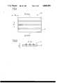
- FIG. 1is a plan view of a printed wiring board in accordance with the present invention.
- FIG. 2is a cross-sectional elevation view along the line 2--2 of FIG. 1;
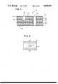
- FIG. 3is a cross-sectional elevation view of a multi-layer printed wiring board in accordance with the present invention.
- FIG. 4is a cross-sectional elevation view of a stripline configuration of a printed wiring board in accordance with the present invention.
- FIG. 5is a cross-sectional elevation view of a "dual" stripline configuration of the printed wiring board in accordance with the present invention.
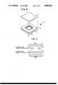
- FIG. 6is an isometric view of a chip carrier package in accordance with the present invention.
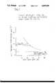
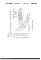
- FIG. 7is a graph of X-Y thermal expansion versus filler content
- FIG. 8is a graph of Z axis thermal expansion versus filler content
- FIG. 9is a graph of backward crosstalk versus line spacing for a printed wiring board in accordance with the present invention.
- FIG. 10is a graph showing solder joint reliability tests.
- FIG. 11is a graph of differential strain versus CTE in the Z direction for several PWB materials.
- the electrical substrate material of the present inventionwhich is well suited for forming printed wiring board (PWB) substrate materials and integrated circuit chip carriers comprises a fluoropolymeric material filled with a coated ceramic material; the electrical substrate material having a low dielectric constant, low loss, low coefficient of thermal expansion, as well as being chemically inert.
- a preferred ceramic materialwhich includes all of the above electrical and physical properties is silica (SiO 2 ), preferably amorphous fused silica powder.
- the ceramici.e., silica
- a material which renders the ceramic surface hydrophobicis normally hydrophilic. It has been found that the ceramic filler used in previously discussed U.S. Pat. No. 4,335,180 leads to the undesired water absorbing properties, low strength, poor copper adhesion and poor dimensional stability of that prior art material.
- this coatingis a silane material such as P-chloromethyl phenyl trimethoxy silane sold under the tradename "PROSIL 246" by Speciality Chemicals Company; "A-40” (chemical composition unknown) also manufactured by Speciality Chemicals Company; amino ethyl amino trimethoxy silane sold under the tradename “DC Z-6020” by Dow Corning Company; and a mixture of phenyl trimethoxy silane (90-95%) and amino ethyl amino propyltrimethoxy silane (5-10%) sold under the tradename "DC X1-6100” also by Dow Corning Company. Of these silane materials, DC X1-6100 has been found to be most preferred.
- silane coatingIn addition to precluding water absorption, the silane coating also leads to several other unexpected improvements including better adhesion, strength and dimensional stabiility (which will be discussed in more detail hereinafter). It has been found that a preferred silane coating for effecting these important features and advantages is 1% by weight of the filler (ceramic) material.
- the fluoropolymer used in the present inventionis polytetrafluoroethylene (PTFE) although examples of other fluoropolymers include copolymers of fluorinated monomers such as hexa fluoropropene (HFP), tetrafluoroethylene (TFE), and perfluoro alkyl vinyl ether (PAVE).
- PTFEpolytetrafluoroethylene
- HFPhexa fluoropropene
- TFEtetrafluoroethylene
- PAVEperfluoro alkyl vinyl ether
- a small amount of microfiberglassi.e., having a mean diameter on the order of 1 micron is preferred for improved dimensional stability in the X-Y plane.
- relative weight percentages of the respective component materialswhich provide the electrical and thermal advantages described below are 33-40 weight percent fluoropolymer; 55-71 weight percent ceramic filler with at least 1 weight percent (based upon the weight percent of the ceramic filler) silane coating and 0-2 weight percent microfiberglass. Also, it is clear from a review of TABLES 1-3 that the present invention is defined by a volume fraction of ceramic filler of about 50% of the total substrate material.
- a preferred composition for the of the present inventionis 34-36% fluoropolymer (PTFE), 62-64% silica filler (SiO 2 ) having a 1% percent coating of silane thereon, and 1% microfiberglass.
- Additional ceramic (silica) filler(at the expense of PTFE) will result in a lower thermal expansion coefficient, and therefore improved surface mount reliability.
- increased ceramic filler levelresults in lower cohesive strength and higher dimensional change after etching circuit patterns.
- Small levels (1%) of microfiberglassseem to improve dimensional stability after etching; increased fiber content presents processing problems when making sheet thicknesses 2.5 mils and lower.
- PWB 10includes substrate 12 comprised of the ceramic filled fluoropolymeric material of the present invention as described above with a plurality of conductive traces 14 formed on substrate 12 using any suitable and well known technique.
- Multilayer board 16comprises a plurality of layers of substrate material 18, 20 and 22, all of which are comprised of the ceramic filled fluoropolymeric material of the present invention.
- Each substrate layer 18, 20 and 22has a conductive pattern 23, 24, 25 and 26 respectively thereon.
- a substrate layer having a circuit pattern thereondefines a circuit substrate. Plated through holes 27 and 28 interconnect selected circuit patterns in a known manner.
- separate sheets 29 and 30 of substrate material having the composition discussed aboveare used as an adhesive or bond ply to laminate individual circuit substrates together.
- a stack-up of circuit substrates alternated with one or more layers of the bond plyis made. This stack-up is then fusion bonded at a high temperature whereby the entire multilayer assembly is melted and fused into a homogeneous construction with consistent electrical and mechanical properties throughout.
- the adhesive bond ply layers 29 and 30may be used to laminate circuit substrates comprised of materials other than the silane coated ceramic filled fluoropolymer of the present invention.
- a multilayer circuit boardindludes circuit substrates and interleaved bond plys which are all comprised of the electrical substrate material of the present invention.
- FIGS. 4 and 5relate respectively to well known stripline and "dual" stripline configurations of the present invention.
- the printed wiring board 10 of FIGS. 1 and 2is sandwiched between a pair of metal ground shields 31 and 31'. It will be appreciated that if only one ground shield 31 is utilized, a conventional microstrip configuration will be provided.
- FIG. 5sets forth a derivation of the stripline of FIG. 4.
- conductors 32 and 34are oriented in either the "X" direction or the "Y" direction defining a "dual" stripline configuration.
- a leadless chip carrier packageis shown generally at 34 and includes a plurality of conductive pads 36 about the periphery thereof and a cavity 38 for accepting an integrated circuit.
- a cover 40also comprised of the circuit substrate described hereinabove, is provided on the top surface 42 of chip carrier 34.
- the process used in manufacturing the electrical substrate material of the present inventionis essentially the same as the manufacturing process described in detail in U.S. Pat. No. 4,335,180, which has previously been incorporated herein by reference.
- the primary difference between the two processesis the additional step in the present invention of coating the ceramic filler particles with a silane coupling agent.
- the ceramic filler particlesare coated using the following procedure:
- dipropylene glycol lubricantis used at a level of 19% weight percent based on total material weight.
- Typical conditionsare; 1700 psi pressure for entire cycle; heat from room temperature to 700° F. at about 3° F./min, hold for 30 minutes, cool at about 1° F./min to 500° F., cool at max rate (about 20° F./min) to room temp.
- Examples 1-8show how filler level, coating level, fiber type and level affect key properties for printed circuit boards.
- the exampleswere prepared in accordance with the method described hereinabove.
- the results outlined in Table 1show that an optimal cross-section of properties occurs at 63% silica filler having been coated with a DC X1-6100 silane coating. This preferred level results in low porosity, very low water absorption, high copper adhesion, improved strength and better dimensional stability.
- the amount of silane coatingis varied between 0% and 4.0% to show how changes in the level of silane effect key properties of the electrical substrate material of the present invention.
- silane levels above 1%seem to favor coupling to the copper foil which result in further improvements to peel strength.
- the preferred amount of silaneis at least 1% and more preferably in the range of between 1 and 2% of the total weight of ceramic filler.
- Examples 15-19four different types of thermally stable silane coatings are compared to a control having no silane coating. All coatings are done at 1% levels. As shown in TABLE 3, all coatings provide dramatic, suprising and unexpected results in terms of reducing water absorption, improving copper adhesion and improving strength. As mentioned, DC X1-6100 is the preferred coating due to thermal stability and consistency of the below listed favorable results.
- FIG. 7is a graphical representation showing the effect of filler level on the X-Y plane thermal expansion coefficient of the material of the present invention. The measurements were taken on a plurality of samples (having varying amounts of filler) as measured on a thermo-mechanical analyzer over a temperature range of 0°-120° C. It will be appreciated that although it is difficult to match the thermal expansion of ceramics, it has been demonstrated (see FIG. 10 discussed below) that CTE's in the 10-20 ppm °C. -1 range can result in high solder joint reliability, as stresses are kept at a minimum due to the high degree of compliancy of the material of the present invention. Thus, as shown in FIG. 7, at relatively high percentages of ceramic filler, the CTE lessens and approaches that of ceramics.
- FIG. 8shows the effect of varying the amount of filler level on the Z-direction thermal expansion coefficient also as measured by a thermo-mechanical analyzer over a temperature range of 0°-120° C. Again, at high filler levels, the Z-direction CTE goes steadily downwardly (see also FIG. 11 discussed below). Significantly, as is evident in both FIGS. 7 and 8, the X-Y and Z direction CTE's may be tailored to favor copper, ceramic or other materials simply by adjusting filler levels.
- Table 4shows the effect of fiber level and filler size distribution on processing thin (i.e., 0.0015") sheet materials (all of the samples having a ceramic filler content of about 62%).
- Sampleswere made (1) with standard filler size distribution (mean particle diameter of roughly 10-15 ⁇ m); (2) with equal to or greater than 30 ⁇ m particles removed; (3) with 1% glass fiber; and (4) with no glass fiber.
- standard filler size distributionmean particle diameter of roughly 10-15 ⁇ m
- the resultsclearly show that manufacture of very thin sheet materials is much easier for compositions without glass fibers and without filler particles having a larger mean particle dimension.
- the electrical substrate material of the present inventionrelative to known prior art substrate materials are set forth below and are divided into two parts: electrical performance; and surface mount reliability.
- the performance of the present invention(RO-2800) is compared to other prior art PWB substrate materials and integrated circuit chip carriers such as PTFE/microfiberglass, epoxy/woven glass, polyimide/woven glass, PTFE/woven glass, polyimide/woven quartz, and polyimide/Kevlar (a registered trademark of E.I. duPont de Nemours Co.).
- the silane coated ceramic filled fluoropolymer PWB substrate material in accordance with the present invention(RO-2800) is the lowest dielectric constant PWB material with respectable performance for surface mount applications, as will be demonstrated hereinafter.
- a dielectric constant of 2.8-2.9propagation delays can be reduced by as much as 30% compared with the woven glass fabric reinforced epoxy and polyimide materials, and by as much as 10% over polyimide laminates reinforced with quartz or Kevlar fabric.
- This datais summarized in TABLE 5. It will be appreciated that while PTFE/microfiberglass materials do exhibit lower dielectric constants and propagation delays relative to the present invention, the adverse thermo-mechanical properties of these materials make them unsuitable for surface mount applications.
- Crosstalkcan be defined as undesirable coupling of energy between signal traces.
- circuit densitiesare very high, resulting in small spacing between traces.
- crosstalkbecomes a major problem.
- the "dual" stripline geometry shown in FIG. 5was used because of its widespread use in multi-layer constructions.
- the line widthswere held constant at 0.005", and the total ground plane spacing was chosen to maintain a nominal characteristic impedance of 50 ohms when the X and Y direction signal layers were separated by 0.005" dielectric.
- FIG. 9a 6 mil space between signal traces would result in less than 2% crosstalk for the present invention (RO-2800), compared to an 8 mil space required for polyimide/quartz and 11.5 mil space required for epoxy/glass. These differences are very significant in high performance applications, enabling circuit designers to route traces closer to one another when using the novel PWB substrate in accordance with the present invention.
- a Tektronix 7854 oscilloscope with the 7S12 TDR plug-in modulewas used for all tests. Trace lengths were 19.6 inches long, the TDR rise-time was typically 25 psec and input rise-time was typically 137 psec.
- the first effectcan be attributed to the difference in dissipation factors for the various materials tested, particularly at high frequencies. Attenuation of the high frequency components of a signal pulse results in a less sharply defined pulse and therefore, rise-time degradation.
- PTFE/microfiberglass and RO-2800 laminatesexhibit low dissipation factors well into the GHz range, with values at 10 GHz as low as 0.0008 and 0.002 respectively. Data describing the dissipation factor at high frequencies could not be found for the other materials tested. However, even at 1 MHz, the dissipation factors are in the 0.01 to 0.02 range.
- RO-2800present invention
- PTFE/microfiberglassthe lowest loss material, PTFE/microfiberglass, resulted in the lowest rise-time degradation, exhibiting an 18% improvement over the present invention (RO-2800).
- a number of transmission line parametersaffect the attenuation of microwave signals in stripline, including: Zo, ⁇ r , loss tangent or dissipation factor, conductor resistivity, surface finishes, conductor thicknesses, and circuit configurations.
- aluminais often used as a chip carrier material
- copperis usually the metal conductor on a PWB.
- All of the other materialsare PWB materials that can be separated into the following categories: fluoropolymer materials (PTFE/glass, RO-2800), specialty reinforcements (polyimide/quartz, polyimide/KEVLAR) and conventional materials (polyimide/glass, epoxy/glass).
- the present inventionwas evaluated for use in surface mount applications by thermal cycling test boards populated with leadless ceramic chip carriers.
- RO-2800Asolder joint failure versus thermal cycle number for each material in Table 8 are graphically shown in FIG. 10.
- the performance of the present invention(RO-2800A) is superior to that of standard epoxy/glass substrates and glass-reinforced fluoropolymer materials, and only slightly less reliable than polyimide/Kevlar and polyimide-quartz boards. If additional filler is added to RO-2800 to reduce the X-Y CTE to approximately 10 ppm °C., then surface mount reliability can be even better than the polyimide quartz boards. A material with this additional filler is identified as RO-2800B in FIG. 10.
- the differential strainis reduced, resulting in reduced stress at the solder joints of surface mounted LCCC's.
- the CTE of the present inventionis not as closely matched to ceramic chip carriers as some other substrate alternatives, its compliant nature plays a major role in reducing stress at the solder joint. This results in surface mount reliability that is comparable to these other materials for 28 and 68 I/0 LCCC's.
- FIG. 11is a graphical representation of the effect of substrate CTE on plated through hole (PTH) reliability.
- PTHplated through hole
- the PWB substrate material of the present inventionexhibits improved electrical performance over other materials being considered for high speed digital applications.
- a PWB material that offers designers improved electrical performance, and a substrate suitable for SMT with reliable plated through holeswill go a long way toward optimizing the interconnection system, complementing the performance of high speed logic devices.
Landscapes
- Chemical & Material Sciences (AREA)
- Physics & Mathematics (AREA)
- Engineering & Computer Science (AREA)
- Microelectronics & Electronic Packaging (AREA)
- Condensed Matter Physics & Semiconductors (AREA)
- Power Engineering (AREA)
- Chemical Kinetics & Catalysis (AREA)
- Medicinal Chemistry (AREA)
- Polymers & Plastics (AREA)
- Organic Chemistry (AREA)
- Spectroscopy & Molecular Physics (AREA)
- General Physics & Mathematics (AREA)
- Computer Hardware Design (AREA)
- Health & Medical Sciences (AREA)
- Compositions Of Macromolecular Compounds (AREA)
- Laminated Bodies (AREA)
- Paints Or Removers (AREA)
- Production Of Multi-Layered Print Wiring Board (AREA)
- Manufacturing Of Printed Wiring (AREA)
- Organic Insulating Materials (AREA)
- Adhesives Or Adhesive Processes (AREA)
Abstract
Description
______________________________________ Silane Coating Level Required Floculant Level ______________________________________ 0% 0.2 parts per 100 parts filler 0.25% 0.13 parts per 100 parts filler 0.5% 0.11 parts per 100 parts filler 2.0% 0.10 parts per 100 parts filler ______________________________________
TABLE 1 __________________________________________________________________________EXAMPLE 1 2 3 4 5 6 7 8 __________________________________________________________________________Coating type DC DC DC DC X16100 X16100 X16100 X16100 Coating level (%) 0 0 0 0 1.0 1.0 1.0 1.0 Filler level (%) 71 71 63 63 71 63 71 63 Fiber type Glass Kevlar Glass Kevlar Kevlar Kevlar Glass Glass Fiber Level (%) 1.0 1.0 1.0 1.0 1.0 1.0 1.0 1.0 Ash Content (%) 10.5 68.1 59.9 61.0 69.2 60.9 70.5 62.1 Density (g/cm.sup.3) 1.777 1.840 2.037 2.003 1.885 2.104 1.925 2.074 Porosity (Vol %) 18.1 14.7 6.1 7.1 12.6 2.4 11.3 4.4 Water Absorption (%) 48 hr, 50° C. 2.758 2.018 1.580 1.960 0.594 0.123 0.773 0.058 Peel Strength (lb/inch) 1.61 1.10 2.00 5.48 5.62 5.81 2.58 9.80 Young's Modulus (kpsi) 11.95 -- 24.85 27.40 36.20 129.50 60.15 66.70 Tensile Strength (psi) 298 -- 414 720 818 1695 956 1407 X-Y CTE (0-120° C.) (ppm°C..sup.-1) 12 10 17 15 10 19 11 17 Z-dir CTE (0-120° C.) (ppm°C..sup.-1) 6 7 15 16 15 20 10 23 Dim. Stability, X-dir + + + + + - + + (mils/inch) 3.986 3.417 2.483 2.820 2.596 0.144 1.884 0.705 Dim. Stability, Y-dir + + + + + - + + (mils/inch) 4.121 3.527 2.451 2.789 2.771 0.189 1.995 0.821 Dielectric Constant 2.64 2.75 2.83 2.78 2.76 2.91 2.84 2.85 Dissipation Factor .0023 .0046 .0026 .0022 .0017 .0024 .0034 .0016 Filler Volume Fraction 0.569 0.569 0.554 0.554 0.593 0.581 0.612 0.584 (%) __________________________________________________________________________
TABLE 2 __________________________________________________________________________ Filler Volume WATER Fraction (%) ASH ABSORPTION X-Y CTE, Z-dir CTE (Assuming X1 = EX- SILANE CON- 24 hr, 48 hr, PEEL YOUNG'S TENSILE 0-120° C., 0-120° C., (ASH)/(100) - AM-LEVEL TENT 23° C. 50° C. STRENGTH MODULUS STRENGTH (ppm (ppm .01 where PLE (%) (%) (%) (%) (lb/inch) (psi) (psi) °C..sup.-1) °C..sup.-1) ASH = 2.0 __________________________________________________________________________ g/cm.sup.3) 9 0 60.2 1.777 1.651 5.7 25,000 600 14 19 approx. 0.546 10 0.25 60.4 0.312 0.305 7.2 143,000 1630 16 26 approx. 0.547 11 0.50 60.8 0.124 0.121 8.0 125,000 1850 16 27 approx. 0.551 12 1.0 61.0 0.111 0.096 6.8 132,000 1890 17 26 approx. 0.553 13 2.0 60.2 0.108 0.076 11.1 81,000 1490 20 35 approx. 0.546 14 4.0 56.7 0.105 0.080 15.1 61,000 1530 22 35 approx. __________________________________________________________________________ 0.513
TABLE 3 __________________________________________________________________________ Filler Volume DI- DIS- Fraction (%) YOUNG'S ELEC- SIPA- (Assuming X1 = EX- DEN- 24 hr, 48 hr, PEEL MODU- TENSILE TRIC TION (ASH)/(100) - AM-ASH SITY 50° C. 50° C. STRENGTH LUS STRENGTH CON- FAC- .01 where PLES COATING (%) (g/cm.sup.3) (%) (%) (lb/inch) (kpsi) (psi) STANT TOR ASH = 2.0 __________________________________________________________________________ g/cm.sup.3) 15 Prosil 246 51.9 2.160 0.218 0.246 9.3 97 1200 2.84 0.0015 approx. 0.507 @ 1% 16 A-50 50.8 2.168 0.681 0.690 8.8 102 1200 2.83 0.0017 approx. 0.498 @ 1% 17 DC 51.8 2.162 0.217 0.248 10.5 99 1300 2.84 0.0015 approx. 0.506 X1-6100 @ 1% 18 DC Z-6020 52.6 2.150 0.569 0.575 9.9 120 1150 2.83 0.0016 approx. 0.511 @ 1% 19 No Coating 51.6 2.160 0.895 7.8 91 900 2.83 0.0016 approx. __________________________________________________________________________ 0.504
TABLE 4 ______________________________________ Effect of Fiber Level & Filler Size Distribution on processing of 0.0015" sheet materals Standard Filler Standard Filler w/ size distribution allparticles 30 μm removed ______________________________________ 1% glass Many pinholes Few pinholes fiber poor edge quality poor edge quality (tears) (tears) unable to reach 0.0015" in 5 calender passes 0% glass Many pinholes No pinholes fiber good edge quality good edge quality ______________________________________
TABLE 5 ______________________________________ Effect of Dielectric Constant on Propagation Delay Propagation Dielectric Dielectric Delay Speed Material Constant (nsec/foot) Efficiency* ______________________________________ Air 1.0 1.0167 100% PTFE/ 2.2 1.5080 67% Microfiberglass RO-2800 (Present 2.8 1.7012 60% Invention) Polyimide/Woven 3.35 1.8609 55% Quartz Polyimide/Woven 3.6 1.9291 53% Kevlar Polyimide/Woven 4.5 2.1567 47% Glass Epoxy/Woven Glass 4.8 2.2275 46% ______________________________________ ##STR1##
TABLE 6 ______________________________________ Rise-Time Degradation Tr Tr/L Material W(mils) Zo(ohms) (psec) (psec/ft) ______________________________________ PTFE/Microfiberglass 4.8 64 139 86 PTFE/Microfiberglass 5.1 79 111 68 RO-2800 5.0 49 165 102 RO-2800 4.4 51 165 102 RO-2800 5.1 69 139 86 RO-2800 5.2 75 139 86 Epoxy/Woven Glass 4.9 51 366 225 Epoxy/Woven Glass 4.7 75 303 187 Polyimide/Woven Glass 5.9 58 236 145 Polyimide/Woven Glass 3.9 74 259 159 ______________________________________ Stripline circuits, trace length (L) = 19.6 inches Tr = (Tr.sub.o.sup.2 -Tr.sub.i.sup.2).sup.1/2 = risetime degradation Tr/L = rise = time degradation per unit trace length
TABLE 7 ______________________________________ Transmission Loss Versus Frequency, RO-2800 Versus "Microwave Material" Transmission Loss (db/inch) Frequency (GHz) RO-2800 PTFE/Microfiberglass ______________________________________ 0.001 9.6 × 10.sup.-5 9.5 × 10.sup.-5 0.001 9.6 × 10.sup.-4 9.5 × 10.sup.-4 0.1 9.6 × 10.sup.-3 9.5 × 10.sup.-3 0.25 0.022 0.024 0.5 0.048 0.048 1.0 0.096 0.095 5.0 0.479 0.477 10.0 0.957 0.953 ______________________________________ 50 ohm stripline 5 mil line width, 1 ounce ED copper
TABLE 8 __________________________________________________________________________THERMAL/MECHANICAL PROPERTIES Thermal Modulus of CTE-xy CTE-z Conductivity Elasticity Density Material (ppm °C.') (ppm °C.') W/m/K (Mpsi) (lb/in.sup.3) __________________________________________________________________________PTFE/glass 24 261 0.26 0.14 0.079 RO2800 16-19 24 0.44 0.1 0.072 Polyimide/quartz 6-8 34 0.13 4.0 0.07 Polyimide/KEVLAR 3.4-6.7 83 0.12 4.0 0.06 Polyimide/glass 11.7-14.2 60 0.35 2.8 0.066 Epoxy/glass 12.8-16 189 0.18 2.5 0.065 Alumina 6.5 6.5 16.8 37.0 0.13 Copper 16.9 16.9 394 17.0 0.324 __________________________________________________________________________
TABLE 9 ______________________________________ FEATURE BENEFITS OVER PRIOR ART ______________________________________ Low dielectric constant High propagation velocity (as much as 25% higher) Low cross-talk (as much as an order of magnitude lower) Reduced Multilayer board thicknesses Low loss at high frequencies Lower rise-time degradation (by as much as 4 times) Suitable for microwave use Low CTE X-Y plane, Suitable for surface mount compliant technology Low CTE Z-direction Excellent plated through hole reliability Excellent ε.sub.r and thickness Improved Zo control control Higher thermal conductivity Better power dissipation ______________________________________
Claims (42)
Priority Applications (13)
| Application Number | Priority Date | Filing Date | Title |
|---|---|---|---|
| US07/015,191US4849284A (en) | 1987-02-17 | 1987-02-17 | Electrical substrate material |
| JP3495388AJP2557248B2 (en) | 1987-02-17 | 1988-02-17 | Electrical substrate material |
| DE198888630026TDE279769T1 (en) | 1987-02-17 | 1988-02-17 | MATERIAL FOR ELECTRIC CARRIER AND MULTI-LAYER CIRCUIT CONTAINING THIS MATERIAL AND INTEGRATED CIRCUIT CHIPBOARD. |
| DE3851553TDE3851553T2 (en) | 1987-02-17 | 1988-02-17 | Material for electrical carriers and multi-layer circuit containing this material and integrated circuit chip carrier. |
| EP19880630026EP0279769B1 (en) | 1987-02-17 | 1988-02-17 | Electrical substrate material, multilayer circuit and integrated circuit chip carrier package comprising said material |
| US07/279,474US5149590A (en) | 1987-02-17 | 1988-12-02 | Electrical substrate material |
| US07/367,241US5061548A (en) | 1987-02-17 | 1989-06-16 | Ceramic filled fluoropolymeric composite material |
| DE19914102441DE4102441A1 (en) | 1987-02-17 | 1991-01-28 | Ceramic-filled fluoro-polymer compsn. for electrical substrates - with silanised filler present to give improved flow properties, e.g. into through-holes |
| US07/703,633US5281466A (en) | 1987-02-17 | 1991-05-22 | Low volume fraction ceramic filled fluoropolymeric composite material |
| US07/704,303US5198295A (en) | 1987-02-17 | 1991-05-22 | Ceramic filled fluoropolymeric composite material |
| US07/704,320US5194326A (en) | 1987-02-17 | 1991-05-22 | Ceramic filled fluoropolymeric composite material |
| US08131870US5384181B1 (en) | 1987-02-17 | 1993-10-05 | Low volume fraction ceramic filled fluoropolymeric composite material |
| US08/379,991USRE36396E (en) | 1987-02-17 | 1995-01-27 | Electrical substrate material comprising amorphous fused silica powder |
Applications Claiming Priority (2)
| Application Number | Priority Date | Filing Date | Title |
|---|---|---|---|
| US07/015,191US4849284A (en) | 1987-02-17 | 1987-02-17 | Electrical substrate material |
| DE19914102441DE4102441A1 (en) | 1987-02-17 | 1991-01-28 | Ceramic-filled fluoro-polymer compsn. for electrical substrates - with silanised filler present to give improved flow properties, e.g. into through-holes |
Related Parent Applications (2)
| Application Number | Title | Priority Date | Filing Date |
|---|---|---|---|
| US07/279,474Continuation-In-PartUS5149590A (en) | 1987-02-17 | 1988-12-02 | Electrical substrate material |
| US07/483,501Continuation-In-PartUS5024871A (en) | 1987-02-17 | 1990-02-21 | Ceramic filled fluoropolymetric composite material |
Related Child Applications (3)
| Application Number | Title | Priority Date | Filing Date |
|---|---|---|---|
| US07/279,474Continuation-In-PartUS5149590A (en) | 1987-02-17 | 1988-12-02 | Electrical substrate material |
| US07/367,241Continuation-In-PartUS5061548A (en) | 1987-02-17 | 1989-06-16 | Ceramic filled fluoropolymeric composite material |
| US08/379,991ReissueUSRE36396E (en) | 1987-02-17 | 1995-01-27 | Electrical substrate material comprising amorphous fused silica powder |
Publications (1)
| Publication Number | Publication Date |
|---|---|
| US4849284Atrue US4849284A (en) | 1989-07-18 |
Family
ID=39534930
Family Applications (1)
| Application Number | Title | Priority Date | Filing Date |
|---|---|---|---|
| US07/015,191CeasedUS4849284A (en) | 1987-02-17 | 1987-02-17 | Electrical substrate material |
Country Status (4)
| Country | Link |
|---|---|
| US (1) | US4849284A (en) |
| EP (1) | EP0279769B1 (en) |
| JP (1) | JP2557248B2 (en) |
| DE (3) | DE3851553T2 (en) |
Cited By (96)
| Publication number | Priority date | Publication date | Assignee | Title |
|---|---|---|---|---|
| WO1990015422A1 (en)* | 1989-06-09 | 1990-12-13 | Rogers Corporation | Coaxial cable insulation and coaxial cable made therefrom |
| US5024871A (en)* | 1990-02-21 | 1991-06-18 | Rogers Corporation | Ceramic filled fluoropolymetric composite material |
| EP0446656A1 (en)* | 1990-03-15 | 1991-09-18 | Rogers Corporation | Method of manufacturing a multilayer circuit board |
| US5055342A (en)* | 1990-02-16 | 1991-10-08 | International Business Machines Corporation | Fluorinated polymeric composition, fabrication thereof and use thereof |
| US5061548A (en)* | 1987-02-17 | 1991-10-29 | Rogers Corporation | Ceramic filled fluoropolymeric composite material |
| US5081562A (en)* | 1987-05-19 | 1992-01-14 | Mitsubishi Denki Kabushiki Kaisha | Circuit board with high heat dissipations characteristic |
| GB2251860A (en)* | 1991-01-17 | 1992-07-22 | Rogers Corp | Ceramic tilled fluoropolymeric composite material |
| DE4102441A1 (en)* | 1987-02-17 | 1992-07-30 | Rogers Corp | Ceramic-filled fluoro-polymer compsn. for electrical substrates - with silanised filler present to give improved flow properties, e.g. into through-holes |
| US5149590A (en)* | 1987-02-17 | 1992-09-22 | Rogers Corporation | Electrical substrate material |
| US5194326A (en)* | 1987-02-17 | 1993-03-16 | Rogers Corporation | Ceramic filled fluoropolymeric composite material |
| US5274912A (en)* | 1992-09-01 | 1994-01-04 | Rogers Corporation | Method of manufacturing a multilayer circuit board |
| US5287619A (en)* | 1992-03-09 | 1994-02-22 | Rogers Corporation | Method of manufacture multichip module substrate |
| US5294476A (en)* | 1988-12-09 | 1994-03-15 | Minnesota Mining And Manufacturing Company | Patterning process and microparticles of substantially the same geometry and shape |
| US5309629A (en)* | 1992-09-01 | 1994-05-10 | Rogers Corporation | Method of manufacturing a multilayer circuit board |
| US5312576A (en)* | 1991-05-24 | 1994-05-17 | Rogers Corporation | Method for making particulate filled composite film |
| US5329695A (en)* | 1992-09-01 | 1994-07-19 | Rogers Corporation | Method of manufacturing a multilayer circuit board |
| US5354611A (en)* | 1990-02-21 | 1994-10-11 | Rogers Corporation | Dielectric composite |
| US5358775A (en)* | 1993-07-29 | 1994-10-25 | Rogers Corporation | Fluoropolymeric electrical substrate material exhibiting low thermal coefficient of dielectric constant |
| US5374453A (en)* | 1991-05-24 | 1994-12-20 | Rogers Corporation | Particulate filled composite film and method of making same |
| US5376759A (en)* | 1993-06-24 | 1994-12-27 | Northern Telecom Limited | Multiple layer printed circuit board |
| US5418690A (en)* | 1993-06-11 | 1995-05-23 | International Business Machines Corporation | Multiple wiring and X section printed circuit board technique |
| US5440805A (en)* | 1992-03-09 | 1995-08-15 | Rogers Corporation | Method of manufacturing a multilayer circuit |
| EP0695116A1 (en) | 1994-07-29 | 1996-01-31 | Rogers Corporation | Fluoropolymer composites containing two or more ceramic fillers to achieve independent control of dielectric constant and dimensional stability |
| US5506049A (en)* | 1991-05-24 | 1996-04-09 | Rogers Corporation | Particulate filled composite film and method of making same |
| US5512711A (en)* | 1992-12-28 | 1996-04-30 | International Business Machines Corporation | Copper-based paste containing refractory metal additions for densification control |
| EP0710699A1 (en) | 1994-11-07 | 1996-05-08 | Rogers Corporation | Ceramic filled composite polymeric electrical substrate material exhibiting high dielectric constant and low thermal coefficient of dielectric constant |
| US5532608A (en)* | 1995-04-06 | 1996-07-02 | International Business Machines Corporation | Ceramic probe card and method for reducing leakage current |
| US5607744A (en)* | 1992-12-29 | 1997-03-04 | International Business Machines Corporation | Coated filler and use thereof |
| US5652055A (en)* | 1994-07-20 | 1997-07-29 | W. L. Gore & Associates, Inc. | Matched low dielectric constant, dimensionally stable adhesive sheet |
| US5717249A (en)* | 1995-04-05 | 1998-02-10 | Matsushita Electronics Corporation | RF power amplifying circuit device |
| US5798563A (en)* | 1997-01-28 | 1998-08-25 | International Business Machines Corporation | Polytetrafluoroethylene thin film chip carrier |
| US5801092A (en)* | 1997-09-04 | 1998-09-01 | Ayers; Michael R. | Method of making two-component nanospheres and their use as a low dielectric constant material for semiconductor devices |
| WO1998044544A1 (en)* | 1997-04-03 | 1998-10-08 | W.L. Gore & Associates, Inc. | Low dielectric constant material with improved dielectric strength |
| WO1998021272A3 (en)* | 1996-10-29 | 1998-10-15 | Richard A Holl | Manufacture of composites of inorganic powder and polymer materials |
| WO1998050945A3 (en)* | 1997-05-07 | 1999-03-11 | Daniel J Skamser | Low density film for low dielectric constant applications |
| US5922453A (en)* | 1997-02-06 | 1999-07-13 | Rogers Corporation | Ceramic-filled fluoropolymer composite containing polymeric powder for high frequency circuit substrates |
| US5948533A (en)* | 1990-02-09 | 1999-09-07 | Ormet Corporation | Vertically interconnected electronic assemblies and compositions useful therefor |
| US6000130A (en)* | 1996-08-28 | 1999-12-14 | International Business Machines Corporation | Process for making planar redistribution structure |
| US6201194B1 (en)* | 1998-12-02 | 2001-03-13 | International Business Machines Corporation | Multi-voltage plane, multi-signal plane circuit card with photoimageable dielectric |
| US6254972B1 (en) | 1999-06-29 | 2001-07-03 | International Business Machines Corporation | Semiconductor device having a thermoset-containing dielectric material and methods for fabricating the same |
| DE4217075C2 (en)* | 1991-05-22 | 2001-08-16 | World Properties Inc | Fluoropolymer composite material with a low volume of ceramic filler |
| US6329062B1 (en) | 2000-02-29 | 2001-12-11 | Novellus Systems, Inc. | Dielectric layer including silicalite crystals and binder and method for producing same for microelectronic circuits |
| US6353182B1 (en)* | 1997-08-18 | 2002-03-05 | International Business Machines Corporation | Proper choice of the encapsulant volumetric CTE for different PGBA substrates |
| US6426147B1 (en) | 1997-08-16 | 2002-07-30 | Basf Coatings Ag | Substrate having a multilayer coat and method for its production |
| US6500529B1 (en) | 2001-09-14 | 2002-12-31 | Tonoga, Ltd. | Low signal loss bonding ply for multilayer circuit boards |
| US6515066B2 (en) | 1998-02-13 | 2003-02-04 | World Properties, Inc. | Casting mixtures comprising granular and dispersion fluoropolymers |
| US6521843B1 (en)* | 1998-05-13 | 2003-02-18 | Nec Corporation | Multilayer printed circuit board having signal, power and ground through holes |
| US6528145B1 (en)* | 2000-06-29 | 2003-03-04 | International Business Machines Corporation | Polymer and ceramic composite electronic substrates |
| US6534186B2 (en)* | 1997-03-19 | 2003-03-18 | International Business Machines Corporation | Chip carriers with enhanced wire bondability |
| US6533855B1 (en) | 2001-02-13 | 2003-03-18 | Novellus Systems, Inc. | Dispersions of silicalite and zeolite nanoparticles in nonpolar solvents |
| US6545227B2 (en)* | 2001-07-11 | 2003-04-08 | Mce/Kdi Corporation | Pocket mounted chip having microstrip line |
| US6605868B2 (en)* | 1998-12-10 | 2003-08-12 | Kabushiki Kaisha Toshiba | Insulating substrate including multilevel insulative ceramic layers joined with an intermediate layer |
| US20030150641A1 (en)* | 2002-02-14 | 2003-08-14 | Noyan Kinayman | Multilayer package for a semiconductor device |
| US6639155B1 (en) | 1997-06-11 | 2003-10-28 | International Business Machines Corporation | High performance packaging platform and method of making same |
| US6783841B2 (en) | 2001-09-14 | 2004-08-31 | Tonoga, Inc. | Low signal loss bonding ply for multilayer circuit boards |
| US20050123739A1 (en)* | 2003-12-04 | 2005-06-09 | Chen-Yang Yui W. | Mesoporous silica/fluorinated polymer composite material |
| US20060011383A1 (en)* | 2004-07-15 | 2006-01-19 | Takashi Noguchi | Multi-layered circuit board assembly |
| US20060180936A1 (en)* | 2004-03-31 | 2006-08-17 | Endicott Interconnect Technologies, Inc. | Fluoropolymer dielectric composition for use in circuitized substrates and circuitized substrate including same |
| US20070141268A1 (en)* | 2005-12-19 | 2007-06-21 | Damon Brink | Composite meterial for printed circuit board applications |
| US20080227904A1 (en)* | 2004-12-23 | 2008-09-18 | Solvay Solexis, Inc. | Thermoplastic Halogenated Polymer Composition |
| US20090166060A1 (en)* | 2006-03-20 | 2009-07-02 | Iji Onozuka | Insulating Resin Layer, Insulating Resin Layer With Carrier And Multiple-Layered Printed Wiring Board |
| US20100087599A1 (en)* | 2007-02-16 | 2010-04-08 | Daikin Industries , Ltd. | Fluororesin composition, fluororesin molded article and method for producing the same |
| US20100084168A1 (en)* | 2008-10-03 | 2010-04-08 | Po-Ju Chou | Manufacturing method of a flexible printed circuit board and a structure thereof |
| US20130048355A1 (en)* | 2011-08-30 | 2013-02-28 | Ibiden Co., Ltd. | Printed wiring board |
| WO2014093775A1 (en)* | 2012-12-13 | 2014-06-19 | Corning Incorporated | Glass and methods of making glass articles |
| US9340443B2 (en) | 2012-12-13 | 2016-05-17 | Corning Incorporated | Bulk annealing of glass sheets |
| US9549468B1 (en)* | 2015-07-13 | 2017-01-17 | Advanced Semiconductor Engineering, Inc. | Semiconductor substrate, semiconductor module and method for manufacturing the same |
| US9862859B2 (en) | 2014-09-12 | 2018-01-09 | W. L. Gore & Associates, Inc. | Porous air permeable polytetrafluoroethylene composites with improved mechanical and thermal properties |
| US9889635B2 (en) | 2012-12-13 | 2018-02-13 | Corning Incorporated | Facilitated processing for controlling bonding between sheet and carrier |
| US10014177B2 (en) | 2012-12-13 | 2018-07-03 | Corning Incorporated | Methods for processing electronic devices |
| US10046542B2 (en) | 2014-01-27 | 2018-08-14 | Corning Incorporated | Articles and methods for controlled bonding of thin sheets with carriers |
| US10086584B2 (en) | 2012-12-13 | 2018-10-02 | Corning Incorporated | Glass articles and methods for controlled bonding of glass sheets with carriers |
| US10510576B2 (en) | 2013-10-14 | 2019-12-17 | Corning Incorporated | Carrier-bonding methods and articles for semiconductor and interposer processing |
| US10543662B2 (en) | 2012-02-08 | 2020-01-28 | Corning Incorporated | Device modified substrate article and methods for making |
| US11097509B2 (en) | 2016-08-30 | 2021-08-24 | Corning Incorporated | Siloxane plasma polymers for sheet bonding |
| CN113475169A (en)* | 2019-02-27 | 2021-10-01 | 罗杰斯公司 | Low loss dielectric composite comprising hydrophobized fused silica |
| US11167532B2 (en) | 2015-05-19 | 2021-11-09 | Corning Incorporated | Articles and methods for bonding sheets with carriers |
| CN113658742A (en)* | 2021-10-21 | 2021-11-16 | 西安宏星电子浆料科技股份有限公司 | Organic gold conductor slurry |
| US11192340B2 (en) | 2014-04-09 | 2021-12-07 | Corning Incorporated | Device modified substrate article and methods for making |
| US11331692B2 (en) | 2017-12-15 | 2022-05-17 | Corning Incorporated | Methods for treating a substrate and method for making articles comprising bonded sheets |
| US11472165B2 (en)* | 2018-07-31 | 2022-10-18 | Nitto Denko Corporation | Plate-like composite material |
| US11535553B2 (en) | 2016-08-31 | 2022-12-27 | Corning Incorporated | Articles of controllably bonded sheets and methods for making same |
| US11549035B2 (en) | 2020-12-16 | 2023-01-10 | Saint-Gobain Performance Plastics Corporation | Dielectric substrate and method of forming the same |
| WO2023016242A1 (en)* | 2021-08-12 | 2023-02-16 | 广东生益科技股份有限公司 | Fluorine-containing resin-based resin composition and application thereof |
| US11596064B2 (en) | 2020-07-28 | 2023-02-28 | Saint-Gobain Performance Plastics Corporation | Dielectric substrate and method of forming the same |
| US20230192972A1 (en)* | 2020-12-09 | 2023-06-22 | Shengyi Technology Co., Ltd. | Fluorine-Containing Resin Composition, and Resin Vanish, Fluorine-Containing Dielectric Sheet, Laminate, Copper Clad Laminate and Printed Circuit Board Containing the Same |
| US11818838B2 (en) | 2019-06-21 | 2023-11-14 | Taiwan Union Technology Corporation | Metal-clad laminate and manufacturing method of the same |
| US11840047B2 (en) | 2019-09-04 | 2023-12-12 | Taiwan Union Technology Corporation | Metal-clad laminate, printed circuit board, and method for manufacturing the same |
| US11905201B2 (en) | 2015-06-26 | 2024-02-20 | Corning Incorporated | Methods and articles including a sheet and a carrier |
| USRE49929E1 (en)* | 2017-08-08 | 2024-04-16 | Sumitomo Electric Industries, Ltd. | Substrate for high-frequency printed wiring board |
| US11999135B2 (en) | 2017-08-18 | 2024-06-04 | Corning Incorporated | Temporary bonding using polycationic polymers |
| US20240284596A1 (en)* | 2021-09-27 | 2024-08-22 | Chengdu Boe Optoelectronics Technology Co., Ltd. | Circuit board structure and display device |
| US12173201B2 (en) | 2020-12-16 | 2024-12-24 | Versiv Composites Limited | Copper-clad laminate and method of forming the same |
| US12213249B2 (en) | 2020-05-18 | 2025-01-28 | Sumitomo Electric Industries, Ltd. | Method for manufacturing dielectric sheet, method for manufacturing substrate for high-frequency printed wiring board, dielectric sheet, and substrate for high-frequency printed wiring board |
| US12262468B2 (en) | 2020-07-28 | 2025-03-25 | Versiv Composites Limited | Copper-clad laminate and method of forming the same |
| US12391850B2 (en) | 2020-12-16 | 2025-08-19 | Versiv Composites Limited | Dielectric substrate and method of forming the same |
Families Citing this family (27)
| Publication number | Priority date | Publication date | Assignee | Title |
|---|---|---|---|---|
| US4915981A (en)* | 1988-08-12 | 1990-04-10 | Rogers Corporation | Method of laser drilling fluoropolymer materials |
| EP0436652A1 (en)* | 1988-09-30 | 1991-07-17 | Raychem Limited | Hybrid microchip bonding article |
| CA2006992A1 (en)* | 1989-01-26 | 1990-07-26 | Amr Aly | Powder of plastic and treated mineral |
| US5126192A (en)* | 1990-01-26 | 1992-06-30 | International Business Machines Corporation | Flame retardant, low dielectric constant microsphere filled laminate |
| JPH06119810A (en)* | 1990-02-21 | 1994-04-28 | Rogers Corp | Dielectric composite |
| US5077115A (en)* | 1990-05-08 | 1991-12-31 | Rogers Corporation | Thermoplastic composite material |
| GB2272107A (en)* | 1992-10-31 | 1994-05-04 | Marconi Gec Ltd | Printed circuit board assembly |
| US5670250A (en)* | 1995-02-24 | 1997-09-23 | Polyclad Laminates, Inc. | Circuit board prepreg with reduced dielectric constant |
| US9054094B2 (en) | 1997-04-08 | 2015-06-09 | X2Y Attenuators, Llc | Energy conditioning circuit arrangement for integrated circuit |
| US7336468B2 (en) | 1997-04-08 | 2008-02-26 | X2Y Attenuators, Llc | Arrangement for energy conditioning |
| US7321485B2 (en) | 1997-04-08 | 2008-01-22 | X2Y Attenuators, Llc | Arrangement for energy conditioning |
| US6099677A (en)* | 1998-02-13 | 2000-08-08 | Merrimac Industries, Inc. | Method of making microwave, multifunction modules using fluoropolymer composite substrates |
| AU3886801A (en)* | 1999-09-21 | 2001-04-24 | Saint-Gobain Ceramics And Plastics, Inc. | Thermally conductive materials in a hydrophobic compound for thermal management |
| US6660241B2 (en) | 2000-05-01 | 2003-12-09 | Saint-Gobain Ceramics & Plastics, Inc. | Highly delaminated hexagonal boron nitride powders, process for making, and uses thereof |
| US6794435B2 (en) | 2000-05-18 | 2004-09-21 | Saint Gobain Ceramics & Plastics, Inc. | Agglomerated hexagonal boron nitride powders, method of making, and uses thereof |
| US6764975B1 (en) | 2000-11-28 | 2004-07-20 | Saint-Gobain Ceramics & Plastics, Inc. | Method for making high thermal diffusivity boron nitride powders |
| JP2004525242A (en) | 2001-04-30 | 2004-08-19 | サンーゴバン セラミックス アンド プラスティクス,インコーポレイティド | Polymer processing aid and polymer processing method |
| US6645612B2 (en) | 2001-08-07 | 2003-11-11 | Saint-Gobain Ceramics & Plastics, Inc. | High solids hBN slurry, hBN paste, spherical hBN powder, and methods of making and using them |
| US6632511B2 (en) | 2001-11-09 | 2003-10-14 | Polyclad Laminates, Inc. | Manufacture of prepregs and laminates with relatively low dielectric constant for printed circuit boards |
| US7494635B2 (en) | 2003-08-21 | 2009-02-24 | Saint-Gobain Ceramics & Plastics, Inc. | Boron nitride agglomerated powder |
| JP2008535207A (en) | 2005-03-01 | 2008-08-28 | エックストゥーワイ アテニュエイターズ,エルエルシー | Regulator with coplanar conductor |
| DE102015100771B4 (en) | 2015-01-20 | 2022-05-05 | Infineon Technologies Ag | Chip carrier laminate with high-frequency dielectric and thermomechanical damper |
| CN107641276B (en)* | 2017-07-17 | 2018-07-27 | 常州中英科技股份有限公司 | It is a kind of without fibre-reinforced fluorine resin base copper-clad plate and preparation method thereof |
| CN108559208A (en)* | 2018-04-18 | 2018-09-21 | 安徽斯瑞尔阀门有限公司 | A kind of ceramic modified ptfe composite of valve seal nano microcrystalline |
| CN114174415A (en) | 2019-08-06 | 2022-03-11 | Agc株式会社 | Substrate and metal laminate |
| EP4600973A1 (en) | 2022-10-07 | 2025-08-13 | Daikin Industries, Ltd. | Dielectric and method of manufacturing same |
| WO2024128221A1 (en)* | 2022-12-13 | 2024-06-20 | ダイキン工業株式会社 | Composition, sheet and method for producing same |
Citations (6)
| Publication number | Priority date | Publication date | Assignee | Title |
|---|---|---|---|---|
| US4036807A (en)* | 1972-05-22 | 1977-07-19 | Imperial Chemical Industries Limited | Fluorine-containing organosilicon compounds |
| US4251432A (en)* | 1978-03-06 | 1981-02-17 | Trw Inc. | Method of providing curable fluoroelastomer gums having coupling agent coated particulate carbonaceous fillers |
| US4335180A (en)* | 1978-12-26 | 1982-06-15 | Rogers Corporation | Microwave circuit boards |
| US4634631A (en)* | 1985-07-15 | 1987-01-06 | Rogers Corporation | Flexible circuit laminate and method of making the same |
| US4647508A (en)* | 1984-07-09 | 1987-03-03 | Rogers Corporation | Flexible circuit laminate |
| US4696851A (en)* | 1985-03-25 | 1987-09-29 | Olin Corporation | Hybrid and multi-layer circuitry |
Family Cites Families (3)
| Publication number | Priority date | Publication date | Assignee | Title |
|---|---|---|---|---|
| DE1615961A1 (en)* | 1967-04-12 | 1970-06-25 | Degussa | Process for the production of printed circuits |
| NL6818428A (en)* | 1967-12-29 | 1969-07-01 | ||
| US4849284A (en)* | 1987-02-17 | 1989-07-18 | Rogers Corporation | Electrical substrate material |
- 1987
- 1987-02-17USUS07/015,191patent/US4849284A/ennot_activeCeased
- 1988
- 1988-02-17DEDE3851553Tpatent/DE3851553T2/ennot_activeExpired - Lifetime
- 1988-02-17DEDE198888630026Tpatent/DE279769T1/enactivePending
- 1988-02-17EPEP19880630026patent/EP0279769B1/ennot_activeExpired - Lifetime
- 1988-02-17JPJP3495388Apatent/JP2557248B2/ennot_activeExpired - Lifetime
- 1991
- 1991-01-28DEDE19914102441patent/DE4102441A1/ennot_activeCeased
Patent Citations (6)
| Publication number | Priority date | Publication date | Assignee | Title |
|---|---|---|---|---|
| US4036807A (en)* | 1972-05-22 | 1977-07-19 | Imperial Chemical Industries Limited | Fluorine-containing organosilicon compounds |
| US4251432A (en)* | 1978-03-06 | 1981-02-17 | Trw Inc. | Method of providing curable fluoroelastomer gums having coupling agent coated particulate carbonaceous fillers |
| US4335180A (en)* | 1978-12-26 | 1982-06-15 | Rogers Corporation | Microwave circuit boards |
| US4647508A (en)* | 1984-07-09 | 1987-03-03 | Rogers Corporation | Flexible circuit laminate |
| US4696851A (en)* | 1985-03-25 | 1987-09-29 | Olin Corporation | Hybrid and multi-layer circuitry |
| US4634631A (en)* | 1985-07-15 | 1987-01-06 | Rogers Corporation | Flexible circuit laminate and method of making the same |
Cited By (135)
| Publication number | Priority date | Publication date | Assignee | Title |
|---|---|---|---|---|
| US5194326A (en)* | 1987-02-17 | 1993-03-16 | Rogers Corporation | Ceramic filled fluoropolymeric composite material |
| US5061548A (en)* | 1987-02-17 | 1991-10-29 | Rogers Corporation | Ceramic filled fluoropolymeric composite material |
| DE4102441A1 (en)* | 1987-02-17 | 1992-07-30 | Rogers Corp | Ceramic-filled fluoro-polymer compsn. for electrical substrates - with silanised filler present to give improved flow properties, e.g. into through-holes |
| US5149590A (en)* | 1987-02-17 | 1992-09-22 | Rogers Corporation | Electrical substrate material |
| US5081562A (en)* | 1987-05-19 | 1992-01-14 | Mitsubishi Denki Kabushiki Kaisha | Circuit board with high heat dissipations characteristic |
| US5173844A (en)* | 1987-05-19 | 1992-12-22 | Mitsubishi Denki Kabushiki Kaisha | Integrated circuit device having a metal substrate |
| US5294476A (en)* | 1988-12-09 | 1994-03-15 | Minnesota Mining And Manufacturing Company | Patterning process and microparticles of substantially the same geometry and shape |
| US4987274A (en)* | 1989-06-09 | 1991-01-22 | Rogers Corporation | Coaxial cable insulation and coaxial cable made therewith |
| WO1990015422A1 (en)* | 1989-06-09 | 1990-12-13 | Rogers Corporation | Coaxial cable insulation and coaxial cable made therefrom |
| US5948533A (en)* | 1990-02-09 | 1999-09-07 | Ormet Corporation | Vertically interconnected electronic assemblies and compositions useful therefor |
| US5055342A (en)* | 1990-02-16 | 1991-10-08 | International Business Machines Corporation | Fluorinated polymeric composition, fabrication thereof and use thereof |
| US5354611A (en)* | 1990-02-21 | 1994-10-11 | Rogers Corporation | Dielectric composite |
| US5024871A (en)* | 1990-02-21 | 1991-06-18 | Rogers Corporation | Ceramic filled fluoropolymetric composite material |
| EP0443401B1 (en)* | 1990-02-21 | 1997-03-26 | Rogers Corporation | Ceramic filled fluoropolymer composite material |
| EP0446656A1 (en)* | 1990-03-15 | 1991-09-18 | Rogers Corporation | Method of manufacturing a multilayer circuit board |
| GB2251860A (en)* | 1991-01-17 | 1992-07-22 | Rogers Corp | Ceramic tilled fluoropolymeric composite material |
| JP3409066B2 (en) | 1991-01-17 | 2003-05-19 | ワールド プロパティーズ インク. | Fluoropolymer composites filled with low volume fraction ceramic |
| DE4217075C2 (en)* | 1991-05-22 | 2001-08-16 | World Properties Inc | Fluoropolymer composite material with a low volume of ceramic filler |
| DE4217076C2 (en)* | 1991-05-22 | 2001-06-28 | World Properties Inc | Fluoropolymer composite material with ceramic filler |
| US5506049A (en)* | 1991-05-24 | 1996-04-09 | Rogers Corporation | Particulate filled composite film and method of making same |
| US5312576A (en)* | 1991-05-24 | 1994-05-17 | Rogers Corporation | Method for making particulate filled composite film |
| US6172139B1 (en)* | 1991-05-24 | 2001-01-09 | World Properties, Inc. | Particulate filled composition |
| US5374453A (en)* | 1991-05-24 | 1994-12-20 | Rogers Corporation | Particulate filled composite film and method of making same |
| US5287619A (en)* | 1992-03-09 | 1994-02-22 | Rogers Corporation | Method of manufacture multichip module substrate |
| US5440805A (en)* | 1992-03-09 | 1995-08-15 | Rogers Corporation | Method of manufacturing a multilayer circuit |
| US5309629A (en)* | 1992-09-01 | 1994-05-10 | Rogers Corporation | Method of manufacturing a multilayer circuit board |
| US5274912A (en)* | 1992-09-01 | 1994-01-04 | Rogers Corporation | Method of manufacturing a multilayer circuit board |
| US5329695A (en)* | 1992-09-01 | 1994-07-19 | Rogers Corporation | Method of manufacturing a multilayer circuit board |
| US5512711A (en)* | 1992-12-28 | 1996-04-30 | International Business Machines Corporation | Copper-based paste containing refractory metal additions for densification control |
| US5525761A (en)* | 1992-12-28 | 1996-06-11 | International Business Machines Corporation | Copper-based paste containing refractory metal additions for densification control |
| US5614250A (en)* | 1992-12-29 | 1997-03-25 | International Business Machines Corporation | Coated filler and use thereof |
| US5607744A (en)* | 1992-12-29 | 1997-03-04 | International Business Machines Corporation | Coated filler and use thereof |
| US5418690A (en)* | 1993-06-11 | 1995-05-23 | International Business Machines Corporation | Multiple wiring and X section printed circuit board technique |
| US5376759A (en)* | 1993-06-24 | 1994-12-27 | Northern Telecom Limited | Multiple layer printed circuit board |
| FR2708780A1 (en)* | 1993-07-29 | 1995-02-10 | Rogers Corp | Fluoropolymer material with low thermal coefficient of dielectric constant, for electrical substrate. |
| US5358775A (en)* | 1993-07-29 | 1994-10-25 | Rogers Corporation | Fluoropolymeric electrical substrate material exhibiting low thermal coefficient of dielectric constant |
| US5652055A (en)* | 1994-07-20 | 1997-07-29 | W. L. Gore & Associates, Inc. | Matched low dielectric constant, dimensionally stable adhesive sheet |
| EP0695116A1 (en) | 1994-07-29 | 1996-01-31 | Rogers Corporation | Fluoropolymer composites containing two or more ceramic fillers to achieve independent control of dielectric constant and dimensional stability |
| US20050244662A1 (en)* | 1994-07-29 | 2005-11-03 | Horn Allen F Iii | Fluoropolymer composites containing two or more ceramic fillers to achieve independent control of dielectric constant and dimensional stability |
| US5552210A (en)* | 1994-11-07 | 1996-09-03 | Rogers Corporation | Ceramic filled composite polymeric electrical substrate material exhibiting high dielectric constant and low thermal coefficient of dielectric constant |
| EP0710699A1 (en) | 1994-11-07 | 1996-05-08 | Rogers Corporation | Ceramic filled composite polymeric electrical substrate material exhibiting high dielectric constant and low thermal coefficient of dielectric constant |
| US5717249A (en)* | 1995-04-05 | 1998-02-10 | Matsushita Electronics Corporation | RF power amplifying circuit device |
| US5532608A (en)* | 1995-04-06 | 1996-07-02 | International Business Machines Corporation | Ceramic probe card and method for reducing leakage current |
| US6000130A (en)* | 1996-08-28 | 1999-12-14 | International Business Machines Corporation | Process for making planar redistribution structure |
| WO1998021272A3 (en)* | 1996-10-29 | 1998-10-15 | Richard A Holl | Manufacture of composites of inorganic powder and polymer materials |
| US6259037B1 (en) | 1997-01-28 | 2001-07-10 | International Business Machines Corporation | Polytetrafluoroethylene thin film chip carrier |
| US6006428A (en)* | 1997-01-28 | 1999-12-28 | International Business Machines Corporation | Polytetrafluoroethylene thin film chip carrier |
| CN1110088C (en)* | 1997-01-28 | 2003-05-28 | 国际商业机器公司 | Improved polytetrafluoroethyelen thin film chip carrier |
| US5798563A (en)* | 1997-01-28 | 1998-08-25 | International Business Machines Corporation | Polytetrafluoroethylene thin film chip carrier |
| US5922453A (en)* | 1997-02-06 | 1999-07-13 | Rogers Corporation | Ceramic-filled fluoropolymer composite containing polymeric powder for high frequency circuit substrates |
| US6534186B2 (en)* | 1997-03-19 | 2003-03-18 | International Business Machines Corporation | Chip carriers with enhanced wire bondability |
| US5928791A (en)* | 1997-04-03 | 1999-07-27 | W. L. Gore & Associates, Inc. | Low dielectric constant material with improved dielectric strength |
| WO1998044544A1 (en)* | 1997-04-03 | 1998-10-08 | W.L. Gore & Associates, Inc. | Low dielectric constant material with improved dielectric strength |
| WO1998050945A3 (en)* | 1997-05-07 | 1999-03-11 | Daniel J Skamser | Low density film for low dielectric constant applications |
| US6639155B1 (en) | 1997-06-11 | 2003-10-28 | International Business Machines Corporation | High performance packaging platform and method of making same |
| US6426147B1 (en) | 1997-08-16 | 2002-07-30 | Basf Coatings Ag | Substrate having a multilayer coat and method for its production |
| US6353182B1 (en)* | 1997-08-18 | 2002-03-05 | International Business Machines Corporation | Proper choice of the encapsulant volumetric CTE for different PGBA substrates |
| US5801092A (en)* | 1997-09-04 | 1998-09-01 | Ayers; Michael R. | Method of making two-component nanospheres and their use as a low dielectric constant material for semiconductor devices |
| US6515066B2 (en) | 1998-02-13 | 2003-02-04 | World Properties, Inc. | Casting mixtures comprising granular and dispersion fluoropolymers |
| US6521843B1 (en)* | 1998-05-13 | 2003-02-18 | Nec Corporation | Multilayer printed circuit board having signal, power and ground through holes |
| US6201194B1 (en)* | 1998-12-02 | 2001-03-13 | International Business Machines Corporation | Multi-voltage plane, multi-signal plane circuit card with photoimageable dielectric |
| US6605868B2 (en)* | 1998-12-10 | 2003-08-12 | Kabushiki Kaisha Toshiba | Insulating substrate including multilevel insulative ceramic layers joined with an intermediate layer |
| US6254972B1 (en) | 1999-06-29 | 2001-07-03 | International Business Machines Corporation | Semiconductor device having a thermoset-containing dielectric material and methods for fabricating the same |
| US6534160B2 (en) | 1999-06-29 | 2003-03-18 | International Business Machines Corporation | Semiconductor device having a thermoset-containing dielectric material and methods for fabricating the same |
| US7014731B2 (en) | 1999-06-29 | 2006-03-21 | International Business Machines Corporation | Semiconductor device having a thermoset-containing dielectric material and methods for fabricating the same |
| US6329062B1 (en) | 2000-02-29 | 2001-12-11 | Novellus Systems, Inc. | Dielectric layer including silicalite crystals and binder and method for producing same for microelectronic circuits |
| US6528145B1 (en)* | 2000-06-29 | 2003-03-04 | International Business Machines Corporation | Polymer and ceramic composite electronic substrates |
| US6533855B1 (en) | 2001-02-13 | 2003-03-18 | Novellus Systems, Inc. | Dispersions of silicalite and zeolite nanoparticles in nonpolar solvents |
| US6545227B2 (en)* | 2001-07-11 | 2003-04-08 | Mce/Kdi Corporation | Pocket mounted chip having microstrip line |
| US6500529B1 (en) | 2001-09-14 | 2002-12-31 | Tonoga, Ltd. | Low signal loss bonding ply for multilayer circuit boards |
| US6783841B2 (en) | 2001-09-14 | 2004-08-31 | Tonoga, Inc. | Low signal loss bonding ply for multilayer circuit boards |
| US6861092B2 (en) | 2001-09-14 | 2005-03-01 | Tonoga, Inc. | Low signal loss bonding ply for multilayer circuit boards |
| US20050069722A1 (en)* | 2001-09-14 | 2005-03-31 | Tonoga, Inc. | Low signal loss bonding ply for multilayer circuit boards |
| US20030150641A1 (en)* | 2002-02-14 | 2003-08-14 | Noyan Kinayman | Multilayer package for a semiconductor device |
| US20050123739A1 (en)* | 2003-12-04 | 2005-06-09 | Chen-Yang Yui W. | Mesoporous silica/fluorinated polymer composite material |
| US7429789B2 (en) | 2004-03-31 | 2008-09-30 | Endicott Interconnect Technologies, Inc. | Fluoropolymer dielectric composition for use in circuitized substrates and circuitized substrate including same |
| US20060180936A1 (en)* | 2004-03-31 | 2006-08-17 | Endicott Interconnect Technologies, Inc. | Fluoropolymer dielectric composition for use in circuitized substrates and circuitized substrate including same |
| US7309838B2 (en)* | 2004-07-15 | 2007-12-18 | Oki Electric Industry Co., Ltd. | Multi-layered circuit board assembly with improved thermal dissipation |
| US20060011383A1 (en)* | 2004-07-15 | 2006-01-19 | Takashi Noguchi | Multi-layered circuit board assembly |
| US20080227904A1 (en)* | 2004-12-23 | 2008-09-18 | Solvay Solexis, Inc. | Thermoplastic Halogenated Polymer Composition |
| US20070141268A1 (en)* | 2005-12-19 | 2007-06-21 | Damon Brink | Composite meterial for printed circuit board applications |
| US20090166060A1 (en)* | 2006-03-20 | 2009-07-02 | Iji Onozuka | Insulating Resin Layer, Insulating Resin Layer With Carrier And Multiple-Layered Printed Wiring Board |
| US20100087599A1 (en)* | 2007-02-16 | 2010-04-08 | Daikin Industries , Ltd. | Fluororesin composition, fluororesin molded article and method for producing the same |
| US8466236B2 (en) | 2007-02-16 | 2013-06-18 | Daikin Industries, Ltd. | Fluororesin composition, fluororesin molded article and method for producing the same |
| US20100084168A1 (en)* | 2008-10-03 | 2010-04-08 | Po-Ju Chou | Manufacturing method of a flexible printed circuit board and a structure thereof |
| US20100251544A1 (en)* | 2008-10-03 | 2010-10-07 | Po-Ju Chou | Manufacturing method of a flexible printed circuit board |
| CN102970821A (en)* | 2011-08-30 | 2013-03-13 | 揖斐电株式会社 | Printed wiring board |
| US20130048355A1 (en)* | 2011-08-30 | 2013-02-28 | Ibiden Co., Ltd. | Printed wiring board |
| CN102970821B (en)* | 2011-08-30 | 2016-04-20 | 揖斐电株式会社 | Printed substrate |
| US10543662B2 (en) | 2012-02-08 | 2020-01-28 | Corning Incorporated | Device modified substrate article and methods for making |
| WO2014093775A1 (en)* | 2012-12-13 | 2014-06-19 | Corning Incorporated | Glass and methods of making glass articles |
| US20150329415A1 (en)* | 2012-12-13 | 2015-11-19 | Robert Alan Bellman | Glass and methods of making glass articles |
| US9340443B2 (en) | 2012-12-13 | 2016-05-17 | Corning Incorporated | Bulk annealing of glass sheets |
| CN106030686A (en)* | 2012-12-13 | 2016-10-12 | 康宁股份有限公司 | Glass and method of making glass articles |
| US10538452B2 (en) | 2012-12-13 | 2020-01-21 | Corning Incorporated | Bulk annealing of glass sheets |
| US9889635B2 (en) | 2012-12-13 | 2018-02-13 | Corning Incorporated | Facilitated processing for controlling bonding between sheet and carrier |
| US10086584B2 (en) | 2012-12-13 | 2018-10-02 | Corning Incorporated | Glass articles and methods for controlled bonding of glass sheets with carriers |
| US10014177B2 (en) | 2012-12-13 | 2018-07-03 | Corning Incorporated | Methods for processing electronic devices |
| US10510576B2 (en) | 2013-10-14 | 2019-12-17 | Corning Incorporated | Carrier-bonding methods and articles for semiconductor and interposer processing |
| US10046542B2 (en) | 2014-01-27 | 2018-08-14 | Corning Incorporated | Articles and methods for controlled bonding of thin sheets with carriers |
| US11123954B2 (en) | 2014-01-27 | 2021-09-21 | Corning Incorporated | Articles and methods for controlled bonding of thin sheets with carriers |
| US11192340B2 (en) | 2014-04-09 | 2021-12-07 | Corning Incorporated | Device modified substrate article and methods for making |
| US9862859B2 (en) | 2014-09-12 | 2018-01-09 | W. L. Gore & Associates, Inc. | Porous air permeable polytetrafluoroethylene composites with improved mechanical and thermal properties |
| US11167532B2 (en) | 2015-05-19 | 2021-11-09 | Corning Incorporated | Articles and methods for bonding sheets with carriers |
| US11660841B2 (en) | 2015-05-19 | 2023-05-30 | Corning Incorporated | Articles and methods for bonding sheets with carriers |
| US11905201B2 (en) | 2015-06-26 | 2024-02-20 | Corning Incorporated | Methods and articles including a sheet and a carrier |
| US9549468B1 (en)* | 2015-07-13 | 2017-01-17 | Advanced Semiconductor Engineering, Inc. | Semiconductor substrate, semiconductor module and method for manufacturing the same |
| US9966333B2 (en) | 2015-07-13 | 2018-05-08 | Advanced Semiconductor Engineering, Inc. | Semiconductor substrate, semiconductor module and method for manufacturing the same |
| US9812387B2 (en) | 2015-07-13 | 2017-11-07 | Advanced Semiconductor Engineering, Inc. | Semiconductor substrate, semiconductor module and method for manufacturing the same |
| US12122138B2 (en) | 2016-08-30 | 2024-10-22 | Corning Incorporated | Siloxane plasma polymers for sheet bonding |
| US11097509B2 (en) | 2016-08-30 | 2021-08-24 | Corning Incorporated | Siloxane plasma polymers for sheet bonding |
| US12344548B2 (en) | 2016-08-31 | 2025-07-01 | Corning Incorporated | Methods for making controllably bonded sheets |
| US11535553B2 (en) | 2016-08-31 | 2022-12-27 | Corning Incorporated | Articles of controllably bonded sheets and methods for making same |
| USRE49929E1 (en)* | 2017-08-08 | 2024-04-16 | Sumitomo Electric Industries, Ltd. | Substrate for high-frequency printed wiring board |
| US11999135B2 (en) | 2017-08-18 | 2024-06-04 | Corning Incorporated | Temporary bonding using polycationic polymers |
| US11331692B2 (en) | 2017-12-15 | 2022-05-17 | Corning Incorporated | Methods for treating a substrate and method for making articles comprising bonded sheets |
| US11472165B2 (en)* | 2018-07-31 | 2022-10-18 | Nitto Denko Corporation | Plate-like composite material |
| CN113475169A (en)* | 2019-02-27 | 2021-10-01 | 罗杰斯公司 | Low loss dielectric composite comprising hydrophobized fused silica |
| US11818838B2 (en) | 2019-06-21 | 2023-11-14 | Taiwan Union Technology Corporation | Metal-clad laminate and manufacturing method of the same |
| US11840047B2 (en) | 2019-09-04 | 2023-12-12 | Taiwan Union Technology Corporation | Metal-clad laminate, printed circuit board, and method for manufacturing the same |
| US12213249B2 (en) | 2020-05-18 | 2025-01-28 | Sumitomo Electric Industries, Ltd. | Method for manufacturing dielectric sheet, method for manufacturing substrate for high-frequency printed wiring board, dielectric sheet, and substrate for high-frequency printed wiring board |
| US12250767B2 (en) | 2020-07-28 | 2025-03-11 | Versiv Composites Limited | Dielectric substrate and method of forming the same |
| US12262468B2 (en) | 2020-07-28 | 2025-03-25 | Versiv Composites Limited | Copper-clad laminate and method of forming the same |
| US11805600B2 (en) | 2020-07-28 | 2023-10-31 | Saint-Gobain Performance Plastics Corporation | Dielectric substrate and method of forming the same |
| US11596064B2 (en) | 2020-07-28 | 2023-02-28 | Saint-Gobain Performance Plastics Corporation | Dielectric substrate and method of forming the same |
| US20230192972A1 (en)* | 2020-12-09 | 2023-06-22 | Shengyi Technology Co., Ltd. | Fluorine-Containing Resin Composition, and Resin Vanish, Fluorine-Containing Dielectric Sheet, Laminate, Copper Clad Laminate and Printed Circuit Board Containing the Same |
| US11945924B2 (en)* | 2020-12-09 | 2024-04-02 | Shengyi Technology Co., Ltd. | Fluorine-containing resin composition, and resin vanish, fluorine-containing dielectric sheet, laminate, copper clad laminate and printed circuit board containing the same |
| US12049577B2 (en) | 2020-12-16 | 2024-07-30 | Versiv Composites Limited | Dielectric substrate and method of forming the same |
| US12173201B2 (en) | 2020-12-16 | 2024-12-24 | Versiv Composites Limited | Copper-clad laminate and method of forming the same |
| US11549035B2 (en) | 2020-12-16 | 2023-01-10 | Saint-Gobain Performance Plastics Corporation | Dielectric substrate and method of forming the same |
| US12391850B2 (en) | 2020-12-16 | 2025-08-19 | Versiv Composites Limited | Dielectric substrate and method of forming the same |
| WO2023016242A1 (en)* | 2021-08-12 | 2023-02-16 | 广东生益科技股份有限公司 | Fluorine-containing resin-based resin composition and application thereof |
| US20240284596A1 (en)* | 2021-09-27 | 2024-08-22 | Chengdu Boe Optoelectronics Technology Co., Ltd. | Circuit board structure and display device |
| US12439517B2 (en)* | 2021-09-27 | 2025-10-07 | Chengdu Boe Optoelectronics Technology Co., Ltd. | Circuit board structure and display device |
| CN113658742A (en)* | 2021-10-21 | 2021-11-16 | 西安宏星电子浆料科技股份有限公司 | Organic gold conductor slurry |
Also Published As
| Publication number | Publication date |
|---|---|
| JP2557248B2 (en) | 1996-11-27 |
| DE4102441A1 (en) | 1992-07-30 |
| JPS63259907A (en) | 1988-10-27 |
| EP0279769A2 (en) | 1988-08-24 |
| EP0279769B1 (en) | 1994-09-21 |
| DE3851553D1 (en) | 1994-10-27 |
| DE3851553T2 (en) | 1995-02-09 |
| EP0279769A3 (en) | 1990-08-22 |
| DE279769T1 (en) | 1989-03-09 |
Similar Documents
| Publication | Publication Date | Title |
|---|---|---|
| US4849284A (en) | Electrical substrate material | |
| US5149590A (en) | Electrical substrate material | |
| US5055342A (en) | Fluorinated polymeric composition, fabrication thereof and use thereof | |
| US7429789B2 (en) | Fluoropolymer dielectric composition for use in circuitized substrates and circuitized substrate including same | |
| JP7656041B2 (en) | Dielectric substrate and method for forming same | |
| USRE36396E (en) | Electrical substrate material comprising amorphous fused silica powder | |
| JP2023535549A (en) | Dielectric substrate and method of forming the same | |
| JP7539581B2 (en) | Copper-clad laminate and method for forming same | |
| US5194326A (en) | Ceramic filled fluoropolymeric composite material | |
| US6692664B2 (en) | Printed wiring board conductive via hole filler having metal oxide reducing capability | |
| TWI868808B (en) | Dielectric substrate and method of forming the same | |
| JP2023535759A (en) | Dielectric substrate and method of forming the same | |
| US5384181A (en) | Low volume fraction ceramic filled fluoropolymeric composite material | |
| EP4448282A1 (en) | Dielectric substrate and method of forming the same | |
| US5281466A (en) | Low volume fraction ceramic filled fluoropolymeric composite material | |
| KR20220033829A (en) | Printed circuit board and mehod of manufacturing thereof | |
| JPS6252468B2 (en) | ||
| US7931830B2 (en) | Dielectric composition for use in circuitized substrates and circuitized substrate including same | |
| US6228470B1 (en) | Composite substrate for electronic components | |
| Choi et al. | Hybrid prepreg conventional build-up laminate for 112Gbit/s SerDes | |
| US20210045244A1 (en) | Multiple circuit boards with high-density compression interconnect | |
| JP3586792B2 (en) | Fluoropolymer composites filled with low ceramic content | |
| TW202513685A (en) | Prepreg article | |
| KR102812879B1 (en) | Circuit board | |
| JP2002319748A (en) | Base for printed-wiring board and prepreg and printed- wiring board using the prepreg |
Legal Events
| Date | Code | Title | Description |
|---|---|---|---|
| AS | Assignment | Owner name:ROGERS CORPORATION, ONE TECHNOLOGY DRIVE, ROGERS, Free format text:ASSIGNMENT OF ASSIGNORS INTEREST.;ASSIGNORS:ARTHUR, DAVID J.;MOSKO, JOHN C.;JACKSON, CONNIE S.;AND OTHERS;REEL/FRAME:004718/0994;SIGNING DATES FROM 19870416 TO 19870508 | |
| STCF | Information on status: patent grant | Free format text:PATENTED CASE | |
| FEPP | Fee payment procedure | Free format text:PAYOR NUMBER ASSIGNED (ORIGINAL EVENT CODE: ASPN); ENTITY STATUS OF PATENT OWNER: LARGE ENTITY | |
| FPAY | Fee payment | Year of fee payment:4 | |
| AS | Assignment | Owner name:FLEET BANK, NATIONAL ASSOCIATION, CONNECTICUT Free format text:SECURITY INTEREST;ASSIGNOR:ROGERS CORPORATION;REEL/FRAME:006495/0322 Effective date:19930415 | |
| AS | Assignment | Owner name:STATE STREET BANK AND TRUST COMPANY OF CONNECTICUT Free format text:SECURITY INTEREST;ASSIGNOR:ROGERS CORPORATION;REEL/FRAME:006498/0695 Effective date:19930415 | |
| RF | Reissue application filed | Effective date:19950127 | |
| FPAY | Fee payment | Year of fee payment:8 | |
| AS | Assignment | Owner name:WORLD PROPERTIES, INC., ILLINOIS Free format text:ASSIGNMENT OF ASSIGNORS INTEREST;ASSIGNOR:ROGERS CORPORATION;REEL/FRAME:008773/0001 Effective date:19970806 | |
| AS | Assignment | Owner name:ROGERS CORPORATION, CONNECTICUT Free format text:SECURITY RELEASE;ASSIGNOR:FLEET NATIONAL BANK;REEL/FRAME:011306/0786 Effective date:20001102 Owner name:ROGERS CORPORATION, CONNECTICUT Free format text:SECURITY RELEASE;ASSIGNOR:STATE STREET BANK AND TRUST;REEL/FRAME:011306/0812 Effective date:20001024 | |
| AS | Assignment | Owner name:JPMORGAN CHASE BANK, N.A., AS ADMINISTRATIVE AGENT Free format text:SECURITY AGREEMENT;ASSIGNOR:WORLD PROPERTIES, INC.;REEL/FRAME:025438/0024 Effective date:20101123 |