US4845054A - Low temperature chemical vapor deposition of silicon dioxide films - Google Patents
Low temperature chemical vapor deposition of silicon dioxide filmsDownload PDFInfo
- Publication number
- US4845054A US4845054AUS07/068,727US6872787AUS4845054AUS 4845054 AUS4845054 AUS 4845054AUS 6872787 AUS6872787 AUS 6872787AUS 4845054 AUS4845054 AUS 4845054A
- Authority
- US
- United States
- Prior art keywords
- sio
- ozone
- film
- temperature
- temperatures
- Prior art date
- Legal status (The legal status is an assumption and is not a legal conclusion. Google has not performed a legal analysis and makes no representation as to the accuracy of the status listed.)
- Expired - Lifetime
Links
Images

Classifications
- H—ELECTRICITY
- H01—ELECTRIC ELEMENTS
- H01L—SEMICONDUCTOR DEVICES NOT COVERED BY CLASS H10
- H01L21/00—Processes or apparatus adapted for the manufacture or treatment of semiconductor or solid state devices or of parts thereof
- H01L21/02—Manufacture or treatment of semiconductor devices or of parts thereof
- H01L21/02104—Forming layers
- H01L21/02107—Forming insulating materials on a substrate
- H01L21/02109—Forming insulating materials on a substrate characterised by the type of layer, e.g. type of material, porous/non-porous, pre-cursors, mixtures or laminates
- H01L21/02112—Forming insulating materials on a substrate characterised by the type of layer, e.g. type of material, porous/non-porous, pre-cursors, mixtures or laminates characterised by the material of the layer
- H01L21/02123—Forming insulating materials on a substrate characterised by the type of layer, e.g. type of material, porous/non-porous, pre-cursors, mixtures or laminates characterised by the material of the layer the material containing silicon
- H01L21/02164—Forming insulating materials on a substrate characterised by the type of layer, e.g. type of material, porous/non-porous, pre-cursors, mixtures or laminates characterised by the material of the layer the material containing silicon the material being a silicon oxide, e.g. SiO2
- C—CHEMISTRY; METALLURGY
- C23—COATING METALLIC MATERIAL; COATING MATERIAL WITH METALLIC MATERIAL; CHEMICAL SURFACE TREATMENT; DIFFUSION TREATMENT OF METALLIC MATERIAL; COATING BY VACUUM EVAPORATION, BY SPUTTERING, BY ION IMPLANTATION OR BY CHEMICAL VAPOUR DEPOSITION, IN GENERAL; INHIBITING CORROSION OF METALLIC MATERIAL OR INCRUSTATION IN GENERAL
- C23C—COATING METALLIC MATERIAL; COATING MATERIAL WITH METALLIC MATERIAL; SURFACE TREATMENT OF METALLIC MATERIAL BY DIFFUSION INTO THE SURFACE, BY CHEMICAL CONVERSION OR SUBSTITUTION; COATING BY VACUUM EVAPORATION, BY SPUTTERING, BY ION IMPLANTATION OR BY CHEMICAL VAPOUR DEPOSITION, IN GENERAL
- C23C16/00—Chemical coating by decomposition of gaseous compounds, without leaving reaction products of surface material in the coating, i.e. chemical vapour deposition [CVD] processes
- C23C16/22—Chemical coating by decomposition of gaseous compounds, without leaving reaction products of surface material in the coating, i.e. chemical vapour deposition [CVD] processes characterised by the deposition of inorganic material, other than metallic material
- C23C16/30—Deposition of compounds, mixtures or solid solutions, e.g. borides, carbides, nitrides
- C23C16/40—Oxides
- C23C16/401—Oxides containing silicon
- C23C16/402—Silicon dioxide
- H—ELECTRICITY
- H01—ELECTRIC ELEMENTS
- H01L—SEMICONDUCTOR DEVICES NOT COVERED BY CLASS H10
- H01L21/00—Processes or apparatus adapted for the manufacture or treatment of semiconductor or solid state devices or of parts thereof
- H01L21/02—Manufacture or treatment of semiconductor devices or of parts thereof
- H01L21/02104—Forming layers
- H01L21/02107—Forming insulating materials on a substrate
- H01L21/02109—Forming insulating materials on a substrate characterised by the type of layer, e.g. type of material, porous/non-porous, pre-cursors, mixtures or laminates
- H01L21/02112—Forming insulating materials on a substrate characterised by the type of layer, e.g. type of material, porous/non-porous, pre-cursors, mixtures or laminates characterised by the material of the layer
- H01L21/02123—Forming insulating materials on a substrate characterised by the type of layer, e.g. type of material, porous/non-porous, pre-cursors, mixtures or laminates characterised by the material of the layer the material containing silicon
- H01L21/02126—Forming insulating materials on a substrate characterised by the type of layer, e.g. type of material, porous/non-porous, pre-cursors, mixtures or laminates characterised by the material of the layer the material containing silicon the material containing Si, O, and at least one of H, N, C, F, or other non-metal elements, e.g. SiOC, SiOC:H or SiONC
- H01L21/02129—Forming insulating materials on a substrate characterised by the type of layer, e.g. type of material, porous/non-porous, pre-cursors, mixtures or laminates characterised by the material of the layer the material containing silicon the material containing Si, O, and at least one of H, N, C, F, or other non-metal elements, e.g. SiOC, SiOC:H or SiONC the material being boron or phosphorus doped silicon oxides, e.g. BPSG, BSG or PSG
- H—ELECTRICITY
- H01—ELECTRIC ELEMENTS
- H01L—SEMICONDUCTOR DEVICES NOT COVERED BY CLASS H10
- H01L21/00—Processes or apparatus adapted for the manufacture or treatment of semiconductor or solid state devices or of parts thereof
- H01L21/02—Manufacture or treatment of semiconductor devices or of parts thereof
- H01L21/02104—Forming layers
- H01L21/02107—Forming insulating materials on a substrate
- H01L21/02109—Forming insulating materials on a substrate characterised by the type of layer, e.g. type of material, porous/non-porous, pre-cursors, mixtures or laminates
- H01L21/02112—Forming insulating materials on a substrate characterised by the type of layer, e.g. type of material, porous/non-porous, pre-cursors, mixtures or laminates characterised by the material of the layer
- H01L21/02123—Forming insulating materials on a substrate characterised by the type of layer, e.g. type of material, porous/non-porous, pre-cursors, mixtures or laminates characterised by the material of the layer the material containing silicon
- H01L21/02126—Forming insulating materials on a substrate characterised by the type of layer, e.g. type of material, porous/non-porous, pre-cursors, mixtures or laminates characterised by the material of the layer the material containing silicon the material containing Si, O, and at least one of H, N, C, F, or other non-metal elements, e.g. SiOC, SiOC:H or SiONC
- H—ELECTRICITY
- H01—ELECTRIC ELEMENTS
- H01L—SEMICONDUCTOR DEVICES NOT COVERED BY CLASS H10
- H01L21/00—Processes or apparatus adapted for the manufacture or treatment of semiconductor or solid state devices or of parts thereof
- H01L21/02—Manufacture or treatment of semiconductor devices or of parts thereof
- H01L21/02104—Forming layers
- H01L21/02107—Forming insulating materials on a substrate
- H01L21/02109—Forming insulating materials on a substrate characterised by the type of layer, e.g. type of material, porous/non-porous, pre-cursors, mixtures or laminates
- H01L21/02205—Forming insulating materials on a substrate characterised by the type of layer, e.g. type of material, porous/non-porous, pre-cursors, mixtures or laminates the layer being characterised by the precursor material for deposition
- H01L21/02208—Forming insulating materials on a substrate characterised by the type of layer, e.g. type of material, porous/non-porous, pre-cursors, mixtures or laminates the layer being characterised by the precursor material for deposition the precursor containing a compound comprising Si
- H01L21/02214—Forming insulating materials on a substrate characterised by the type of layer, e.g. type of material, porous/non-porous, pre-cursors, mixtures or laminates the layer being characterised by the precursor material for deposition the precursor containing a compound comprising Si the compound comprising silicon and oxygen
- H01L21/02216—Forming insulating materials on a substrate characterised by the type of layer, e.g. type of material, porous/non-porous, pre-cursors, mixtures or laminates the layer being characterised by the precursor material for deposition the precursor containing a compound comprising Si the compound comprising silicon and oxygen the compound being a molecule comprising at least one silicon-oxygen bond and the compound having hydrogen or an organic group attached to the silicon or oxygen, e.g. a siloxane
- H—ELECTRICITY
- H01—ELECTRIC ELEMENTS
- H01L—SEMICONDUCTOR DEVICES NOT COVERED BY CLASS H10
- H01L21/00—Processes or apparatus adapted for the manufacture or treatment of semiconductor or solid state devices or of parts thereof
- H01L21/02—Manufacture or treatment of semiconductor devices or of parts thereof
- H01L21/02104—Forming layers
- H01L21/02107—Forming insulating materials on a substrate
- H01L21/02225—Forming insulating materials on a substrate characterised by the process for the formation of the insulating layer
- H01L21/0226—Forming insulating materials on a substrate characterised by the process for the formation of the insulating layer formation by a deposition process
- H01L21/02263—Forming insulating materials on a substrate characterised by the process for the formation of the insulating layer formation by a deposition process deposition from the gas or vapour phase
- H01L21/02271—Forming insulating materials on a substrate characterised by the process for the formation of the insulating layer formation by a deposition process deposition from the gas or vapour phase deposition by decomposition or reaction of gaseous or vapour phase compounds, i.e. chemical vapour deposition
- Y—GENERAL TAGGING OF NEW TECHNOLOGICAL DEVELOPMENTS; GENERAL TAGGING OF CROSS-SECTIONAL TECHNOLOGIES SPANNING OVER SEVERAL SECTIONS OF THE IPC; TECHNICAL SUBJECTS COVERED BY FORMER USPC CROSS-REFERENCE ART COLLECTIONS [XRACs] AND DIGESTS
- Y10—TECHNICAL SUBJECTS COVERED BY FORMER USPC
- Y10S—TECHNICAL SUBJECTS COVERED BY FORMER USPC CROSS-REFERENCE ART COLLECTIONS [XRACs] AND DIGESTS
- Y10S148/00—Metal treatment
- Y10S148/118—Oxide films
Definitions
- This inventionrelates to a method for depositing an SiO 2 based dielectric film on a semiconductor structure and in particular to a method for low temperature chemical vapor deposition of SiO 2 films using a selected alkoxysilane.
- Tetraethoxysilanehas been used extensively as the source material for the chemical vapor deposition (CVD) of an SiO 2 layer on a semiconductor wafer.
- CVDchemical vapor deposition
- nitrogenis used as the carrier gas which is passed over or bubbled through the TEOS which is held in a source container.
- the wafers to be covered with a deposited SiO 2 filmare laid in a furnace boat in a furnace tube into which the TEOS vapor entrained in the carrier gas is introduced and the wafers are heated to a selected temperature at which the TEOS pyrolytically decomposes.
- the range of temperatures less than approximately 960° C. at which TEOS pyrolytically decomposesis well known. As the temperature of the wafers is reduced the decomposition rate and the film deposition rate decrease until they appear to stop. As a practical matter the range of temperatures typically employed ranges between 650° C.
- the growth rate of the SiO 2 layercan be enhanced by using oxygen as a carrier gas (See U.S. Pat. No. 3,614,584, issued to Inoue on Oct. 19, 1971).
- the Inoue patentalso describes a method for depositing TEOS using tetraethoxysilane as a source together with triisopropyl titanate in order to deposit a composite insulating layer of TiO 2 -SiO 2 where the TiO 2 constitutes less than 0.02% by weight of the layer.
- Inoueemploys the temperature range of 300° C. to 500° C. for the above process.
- Other methods using plasma deposition techniquesare known for depositing an SiO 2 based film on a video disk. For U.S. Pat. No.
- the present inventionutilizes other selected alkoxysilanes which permit the reactions to proceed at lower temperatures and at higher deposition rates.
- the semiconductor structureis heated to a selected temperature less than or equal to 900° C.
- an alkoxysilaneselected from the group consisting of tetramethoxysilane, a trialkoxysilane having the formula ##STR2## where R is a methyl, ethyl or propyl group, a dialkoxysilane having the formula ##STR3## where R is a methyl, ethyl, or propyl group or a vinyltrialkoxysilane having the formula ##STR4## where R is a methyl or ethyl group.
- Oxygen and/or nitrogenare used as a carrier gas with oxygen being preferred.
- the alkoxysilanemay be selected to be tetramethoxysilane, triethoxysilane or trimethoxysilane.
- the reaction temperatureis selected to be between 350° C. and 550° C.
- the alkoxysilane selectedmay be tetramethoxysilane or trimethoxysilane.
- the reaction rateis increased by nearly an order of magnitude for alkoxysilanes.
- this introduction of ozonepermit the reaction to proceed at lower temperatures for a given SiO 2 deposition rate.
- the wafer temperaturemay be selected to be in the range of 350° C. to 500° C. A temperature in this range has distinct advantages in semiconductor processing since it is compatible with the wafer metalization and there is little or no thermal damage to the electrical properties of the circuits embedded in the silicon wafer.
- ozonein the reaction chamber permits the doping of the SiO 2 film with oxides of phosphorous and boron at temperatures between 350° C. and 900° C.
- the use of ozone in this connectionprovides an important advantage over the prior art since it greatly reduces the temperatures at which the doping oxides are formed compared to those required when oxygen alone is used as a carrier gas.
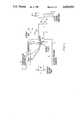
- FIG. 1shows a reactor suitable for employing the methods of this invention.
- FIG. 2shows a reactor similar to FIG. 1 including a second bubble chamber for use in depositing a doped SiO 2 film.
- FIG. 1shows a cross-sectional schematic diagram of a microreactor 10 for employing the methods of the present invention for chemical vapor deposition of an SiO 2 -based dielectric film on a semiconductor structure, for example a silicon wafer.
- Microreactor 10is described in a copending application of Imad Mahawili entitled “Microreactor," U.S. Ser. No. 745,336, now abandoned, filed with the U.S. Patent and Trademark Office on June 14, 1985.
- Microreactor 10includes housing 1 surrounding reactor chamber 2. Housing 1 is made of stainless steel or other inert material which does not react with the gases introduced into chamber 2.
- Heater plate 3, typically a block made of stainless steel,is held in position in chamber 2 by support rod 5 attached to housing 1.
- Silicon wafer 4, upon which the SiO 2 -based film is to be deposited,is placed on heater plate 3. The temperature of plate 3 is regulated by temperature controller 6 which is connected through thermocouple 7 to a cartridge heater embedded in heater plate 3.
- Silicon wafer 4rests upon heater plate 3 and is heated thereby to a selected temperature as determined by temperature controller 6.
- Reactor 10can be operated in the isothermal or cold-wall modes for a range of temperatures from room temperature up to 900° C.
- Exhaust chamber 14is connected to a vacuum pump (not shown) so that microreactor 10 can be operated at reduced pressures, if desired.
- reactor 10was operated at pressures ranging from atmospheric pressure down to 0.5 torr.
- An alkoxysilane 9is introduced into bubble chamber 8 at atmospheric pressure and room temperature (at room temperature, alkoxysilanes are generally in liquid form).
- a carrier gassuch as nitrogen or oxygen is introduced via gas line L 1 .
- the flow rate of the carrier gas into alkoxysilane 9 in bubble chamber 8is regulated by control valve V 1 .
- the carrier gas, together with alkoxysilane vapor,flows from bubble chamber 8 via gas line L 2 to the elongated portion 11 of reactor chamber 2 as shown in FIG. 1.
- the flow rate through line L 2is controlled by valve V 2 .
- a second selected mixture of one or more gasesfor example oxygen, nitrogen, or ozone, may also be introduced into the elongated portion 11 of chamber 2 via line L 3 , which is regulated by flow rate control valve V 3 .
- the above chemical vapor deposition reactorwas used in order to study the deposition rates of SiO 2 -based films for selected alkoxysilanes not previously used for the chemical vapor deposition of SiO 2 -based films on semiconductor wafers.
- Wafer 4was maintained at various selected temperatures for selected carrier gases introduced via line L 1 and for selected gases introduced via line L 3 .
- the deposition rate for the SiO 2 -based film using prior art alkoxysilane tetraethoxysilane Si(OC 2 H 5 ) 4 (TEOS)was used as a control process. Absolute deposition rates were not measured for the alkoxysilanes tested. However, relative rates were determined by visual inspection of the deposited SiO 2 film.
- the reactorwas operated in both the cold wall mode and the hot wall mode.
- Control process 1was carried out for the specific choices of flow rates, temperatures and pressures indicated in parentheses.
- Si(OCH 3 ) 4having a molecular weight of 152.2 g/mole and a boiling point of 121°-122° C. was used in place of tetraethoxysilane.
- triethoxysilane H-Si(OC 2 H 5 ) 3having a molecular weight of 164.3 g/mole and a boiling point of 131.1° C. was used in place of tetraethoxysilane.
- trimethoxysilane, H-Si(OCH 3 ) 3 , 95% pure, having a molecular weight of 122.2 and a boiling point of 86°-87° C.was used in place of tetraethoxysilane.
- Control process 1 and examples 1 through 3all yielded SiO 2 films with the following relative deposition rates, r: r(tetraethoxysilane) ⁇ r(triethoxysilane) ⁇ r(tetramethoxysilane) ⁇ r(trimethoxysilane).
- control process 2Same as control process 1, except that 99.999% pure 02 was used as the carrier gas via line 1 in place of nitrogen. Again control process 2 was carried out for the specific choices of flow rates, temperatures and pressures within the ranges stated as indicated by the values in parentheses.
- trimethoxysilanewas used in place of tetraethoxysilane.
- Control process 2 and examples 4 through 6all yield SiO 2 films with the following relative deposition rates: r(tetraethoxysilane) ⁇ r(triethoxysilane) ⁇ r(tetramethoxysilane) ⁇ r(trimethoxysilane).
- wafer temperaturewas 550°-650° C. (550° C., 600° C., 650° C.) ⁇ 20° C. were the actual wafer temperatures employed.
- Examples 7, 8 and 9are the same as examples 4, 5 and 6, except that the wafer temperature was a selected temperature in the range 550°-650° C. (550° C., 600° C., 650° C.) ⁇ 20° C. were the wafer temperatures selected.
- the deposition rates in this lower temperature rangewere ordered in the same way as given for examples 4, 5 and 6; however, it was noted that very little SiO 2 film was deposited for TEOS (tetraethoxysilane).
- Examples 10, 11 and 12are the same as examples 4, 5 and 6, except that the wafer temperature was a selected temperature in the range 450° C. to 550° C.
- the temperatures selectedwere 450° C., 500° C., and 550° C. ⁇ 20° C. At these lower temperatures, no SiO 2 film was formed using the control process 4 or the example process number 11.
- An SiO 2 filmwas formed in examples 10 and 12 with the SiO 2 deposition rate r(tetramethoxysilane) ⁇ r(trimethoxysilane).
- the wafer temperaturewas a selected temperature in the range 350°-450° C.
- the selected temperatureswere 350° C., 400° C. and 450° C. ⁇ 20° C.
- Examples 13, 14, and 15are the same as examples 4, 5, and 6 except that the wafer temperature was in the range 350°-450° C. At these reduced temperatures, no SiO 2 film was formed using the method of control process 5 or example 14. A very thin film formed using the process of example 13. A thicker film was formed using the process of example 15, i.e., r(tetramethoxysilane) ⁇ r(trimethoxysilane).
- a good quality SiO 2 based filmis deposited using tetramethoxysilane or trimethoxysilane at wafer temperature as low as 350°-550° C.
- good quality SiO 2 based filmis deposited using tetramethoxysilane, trimethoxysilane, and triethoxysilane at wafer temperatures of 550° C. to 650° C.
- the deposition rate of the SiO 2 based filmwas greater using tetramethoxysilane, trimethoxysilane and triethoxysilane than the deposition rate using TEOS.
- Depositing an SiO 2 based film on an IC silicon wafer using these lower reaction temperatureshas an important advantage over the higher temperature reaction required when using TEOS: the electrical properties of the integrated circuit wafer are less affected by lower temperature processing. For example, lower temperature processing causes less diffusion of dopants in the underlying integrated circuit and is more compatible with aluminum metalization.
- methoxysilanes described abovehas the added advantage that they reduce the amount of residual carbon in the deposited SiO 2 based film, which enhances the dielectric quality of the film.
- alkoxysilanes usedwere tetramethoxysilane, triethoxysilane or trimethoxysilane.
- alkoxysilanesmay be employed with the method of this invention:
- the wafer temperaturemay be reduced to the range of 300°-500° C., a temperature which does not adversely affect the properties of active and passive devices formed in and on the wafer surface;
- Example 16provides one example of the use of ozone in the chemical vapor deposition of SiO 2 based films.
- TEOStetraethoxysilane
- Example 16may be modified by using a mixture of O 2 and nitrogen for the carrier gas via line L 1 or by using a mixture of O 2 , nitrogen and less than 10% ozone by weight for the reactant gas via line L 3 .
- example 16was modified by using a mixture of O 2 and less than 10% ozone modified by using a mixture of O 2 and ozone, where the weight percent of ozone present is greater than 0 percent but less than substantially 10 percent it is preferable to introduce ozone via line L 3 .
- An ozone generator(not shown) containing a standard electrodeless discharge tube and capable of producing a concentration of 10% ozone by weight or less from a feed stream of pure oxygen is attached to line L 3 .
- FIG. 2shows a reactor suitable for producing a doped SiO 2 film.
- FIG. 2is similar to FIG. 1 except that a second bubble chamber 15 is provided which contains a dopant source, for example trimethylphosphite or trimethylborate.
- a carrier gassuch as O 2 or N 2 is introduced into the dopant source via line L 4 , which is controlled by valve V4.
- the doped gaspasses via control valve V 5 and line L 5 into mixing chamber 11.
- ozonereadily oxidizes both phosphorous and boron hydrides and alkoxides which are used as dopant sources for doping SiO 2 films. Moreover, oxidation in the presence of ozone takes place at substantially lower temperatures than when pure O 2 is used as the carrier gas.
- the temperature range shown in example 17is 300°-900° C.
- the preferred temperature rangeis lower for selected alkoxysilanes. For example, for a trialkoxysilane the preferred temperature range is 300°-500° C., which does not damage the underlying semiconductor structure.
- the precise configuration of the deposition reactoris not critical to using the methods of this invention and one of ordinary skill in the art will be able to employ other suitable reactors in view of the disclosures made herein.
Landscapes
- Chemical & Material Sciences (AREA)
- Engineering & Computer Science (AREA)
- Manufacturing & Machinery (AREA)
- General Physics & Mathematics (AREA)
- Physics & Mathematics (AREA)
- Computer Hardware Design (AREA)
- Microelectronics & Electronic Packaging (AREA)
- Power Engineering (AREA)
- Condensed Matter Physics & Semiconductors (AREA)
- Inorganic Chemistry (AREA)
- General Chemical & Material Sciences (AREA)
- Chemical Kinetics & Catalysis (AREA)
- Materials Engineering (AREA)
- Mechanical Engineering (AREA)
- Metallurgy (AREA)
- Organic Chemistry (AREA)
- Formation Of Insulating Films (AREA)
Abstract
Description
______________________________________ CONTROL PROCESS 1 ______________________________________ Alkoxysilane: tetraethoxysilane (TEOS) Si(OC.sub.2 H.sub.5).sub.4, electronic grade 99.9% pure; molecular weight, 208.3 g/mole; boiling point 169° C. Carrier gas via Nitrogen line L.sub.1 : Gas via None (line L.sub.3 off) line L.sub.3 : Flow rate via 20-100 sccm (20, 50, 100) sccm line L.sub.1 : Flow rate via 0 line L.sub.3 Wafer temperature: 650° C.-900° C. (650°, 700°, 750°, 900°) ±20° C. Reaction time: 15-30 minutes (15, 30) minutes Pressure: 1 atmosphere to 0.5 torr (1 atmosphere, (10, 5, 0.5) torr) ______________________________________
______________________________________ Alkoxysilane: tetraethoxysilane, tetramethoxysilane, triethoxysilane, or trimethoxysilane Carrier gas via O.sub.2 or Nitrogen line L.sub.1: Reactant gas via O.sub.2 and less than 10% ozone by line L.sub.3 : weight Flow rate for carrier 20-100 sccm (20, 50, 100) sccm gas via line L.sub.1 : Flow rate for gas 20-200 sccm (20, 50, 100, via line L.sub.3 : 200) sccm Wafer temperature: 300-900° C. (300° C., 350° C., - 400° C., 500° C., 600° C., 700° C., - 800° C., 900° C.) ±20° C. Pressure: 1 atmosphere to 0.5 torr (1 atmosphere, (10, 5, 0.5) torr) ______________________________________ (The values of the parameters in parenthesis indicate the values tested)
______________________________________ Alkoxysilane: any alkoxysilane Carrier gas via Line L.sub.1 : O.sub.2 or Nitrogen Reactant gas via Line L.sub.3 : O.sub.2 and less than 10% ozone by weight Carrier gas via line L.sub.4 : O.sub.2 or Nitrogen Flow rate via line L.sub.1 : 20-100 sccm Flow rate via line L.sub.3 : 20-200 sccm Flow rate via line L.sub.4 : 20-100 sccm Wafer temperature: 300°-900° C. Pressure: 1 atmosphere to 0.5 torr Dopant: trimethylphosphite P(OCH.sub.3).sub.3 ______________________________________
Claims (1)
Priority Applications (1)
| Application Number | Priority Date | Filing Date | Title |
|---|---|---|---|
| US07/068,727US4845054A (en) | 1985-06-14 | 1987-06-29 | Low temperature chemical vapor deposition of silicon dioxide films |
Applications Claiming Priority (2)
| Application Number | Priority Date | Filing Date | Title |
|---|---|---|---|
| US74483885A | 1985-06-14 | 1985-06-14 | |
| US07/068,727US4845054A (en) | 1985-06-14 | 1987-06-29 | Low temperature chemical vapor deposition of silicon dioxide films |
Related Parent Applications (1)
| Application Number | Title | Priority Date | Filing Date |
|---|---|---|---|
| US74483885AContinuation | 1985-06-14 | 1985-06-14 |
Publications (1)
| Publication Number | Publication Date |
|---|---|
| US4845054Atrue US4845054A (en) | 1989-07-04 |
Family
ID=26749290
Family Applications (1)
| Application Number | Title | Priority Date | Filing Date |
|---|---|---|---|
| US07/068,727Expired - LifetimeUS4845054A (en) | 1985-06-14 | 1987-06-29 | Low temperature chemical vapor deposition of silicon dioxide films |
Country Status (1)
| Country | Link |
|---|---|
| US (1) | US4845054A (en) |
Cited By (83)
| Publication number | Priority date | Publication date | Assignee | Title |
|---|---|---|---|---|
| US5013691A (en)* | 1989-07-31 | 1991-05-07 | At&T Bell Laboratories | Anisotropic deposition of silicon dioxide |
| US5051380A (en)* | 1989-12-27 | 1991-09-24 | Semiconductor Process Laboratory Co., Ltd. | Process for producing semiconductor device |
| US5059550A (en)* | 1988-10-25 | 1991-10-22 | Sharp Kabushiki Kaisha | Method of forming an element isolating portion in a semiconductor device |
| EP0470632A3 (en)* | 1990-08-10 | 1993-04-21 | Semiconductor Process Laboratory Co., Ltd. | Method of manufacturing a silicon oxide film and an oxide based glass for semiconductor devices |
| EP0478308A3 (en)* | 1990-09-25 | 1993-04-21 | Kawasaki Steel Corporation | Method of forming interlayer-insulating film |
| US5302555A (en)* | 1991-06-10 | 1994-04-12 | At&T Bell Laboratories | Anisotropic deposition of dielectrics |
| US5314845A (en)* | 1989-09-28 | 1994-05-24 | Applied Materials, Inc. | Two step process for forming void-free oxide layer over stepped surface of semiconductor wafer |
| US5316639A (en)* | 1989-06-05 | 1994-05-31 | Sachiko Okazaki | Dielectric material used for an ozone generator and a method of forming a film to the dielectric material |
| US5324539A (en)* | 1991-04-15 | 1994-06-28 | Semiconductor Process Laboratory | Method for forming CVD thin glass films |
| US5336640A (en)* | 1991-01-28 | 1994-08-09 | Kawasaki Steel Corporation | Method of manufacturing a semiconductor device having an insulating layer composed of a BPSG film and a plasma-CVD silicon nitride film |
| WO1994018356A1 (en)* | 1993-02-04 | 1994-08-18 | Watkins-Johnson Company | Method of manufacturing a glass substrate for a thin film |
| WO1994018702A1 (en)* | 1993-02-04 | 1994-08-18 | Watkins-Johnson Company | A thin film semiconductor device and method |
| US5354387A (en)* | 1989-09-28 | 1994-10-11 | Applied Materials, Inc. | Boron phosphorus silicate glass composite layer on semiconductor wafer |
| US5360646A (en)* | 1992-09-10 | 1994-11-01 | Applied Materials, Inc. | Chemical vapor deposition method of silicon dioxide film |
| US5362526A (en)* | 1986-12-19 | 1994-11-08 | Applied Materials, Inc. | Plasma-enhanced CVD process using TEOS for depositing silicon oxide |
| WO1994027316A1 (en)* | 1993-05-14 | 1994-11-24 | Watkins-Johnson Company | Method of manufacturing side walls and semiconductor device having side walls |
| US5376591A (en)* | 1992-06-05 | 1994-12-27 | Semiconductor Process Laboratory Co., Ltd. | Method for manufacturing semiconductor device |
| US5382550A (en)* | 1993-08-05 | 1995-01-17 | Micron Semiconductor, Inc. | Method of depositing SiO2 on a semiconductor substrate |
| US5413967A (en)* | 1991-05-16 | 1995-05-09 | Kabushiki Kaisha Toshiba | Method of manufacturing semiconductor devices |
| US5459108A (en)* | 1992-10-06 | 1995-10-17 | Sharp Kabushiki Kaisha | Normal pressure CVD process for manufacture of a semiconductor device through reaction of a nitrogen containing organic source with ozone |
| US5462899A (en)* | 1992-11-30 | 1995-10-31 | Nec Corporation | Chemical vapor deposition method for forming SiO2 |
| WO1996000803A1 (en)* | 1994-06-28 | 1996-01-11 | Fei Company | Charged particle deposition of electrically insulating films |
| US5496765A (en)* | 1993-06-23 | 1996-03-05 | Siemens Aktiengesellschaft | Method for manufacturing an insulating trench in a substrate for smart-power technologies |
| US5531183A (en)* | 1994-07-13 | 1996-07-02 | Applied Materials, Inc. | Vaporization sequence for multiple liquid precursors used in semiconductor thin film applications |
| US5605867A (en)* | 1992-03-13 | 1997-02-25 | Kawasaki Steel Corporation | Method of manufacturing insulating film of semiconductor device and apparatus for carrying out the same |
| WO1997022992A1 (en)* | 1995-12-15 | 1997-06-26 | Watkins-Johnson Company | Method of forming dielectric films with reduced metal contamination |
| US5650359A (en)* | 1991-05-06 | 1997-07-22 | Texas Instruments Incorporated | Composite dielectric passivation of high density circuits |
| US5672539A (en)* | 1994-01-14 | 1997-09-30 | Micron Technology, Inc. | Method for forming an improved field isolation structure using ozone enhanced oxidation and tapering |
| US5672388A (en)* | 1994-07-08 | 1997-09-30 | Exxon Research & Engineering Company | Membrane reparation and poer size reduction using interfacial ozone assisted chemical vapor deposition |
| US5755886A (en)* | 1986-12-19 | 1998-05-26 | Applied Materials, Inc. | Apparatus for preventing deposition gases from contacting a selected region of a substrate during deposition processing |
| US5783498A (en)* | 1996-05-28 | 1998-07-21 | Nec Corporation | Method of forming silicon dioxide film containing germanium nanocrystals |
| US5827569A (en)* | 1994-07-29 | 1998-10-27 | Akiyama; Shigeo | Hydrogen separation membrane and process for producing the same |
| US5869406A (en)* | 1995-09-28 | 1999-02-09 | Mosel Vitelic, Inc. | Method for forming insulating layers between polysilicon layers |
| US5998162A (en)* | 1995-05-18 | 1999-12-07 | Biosil Ag | Production of secondary metabolites with plant cells immobilized in a porous inorganic support |
| JP3003425B2 (en) | 1992-09-11 | 2000-01-31 | 東亞合成株式会社 | Method for manufacturing silicon oxide film |
| US6054379A (en)* | 1998-02-11 | 2000-04-25 | Applied Materials, Inc. | Method of depositing a low k dielectric with organo silane |
| US6056024A (en)* | 1993-04-28 | 2000-05-02 | Advanced Delivery & Chemical Systems, Ltd. | Bulk chemical delivery system |
| US6057250A (en)* | 1998-01-27 | 2000-05-02 | International Business Machines Corporation | Low temperature reflow dielectric-fluorinated BPSG |
| US6114216A (en)* | 1996-11-13 | 2000-09-05 | Applied Materials, Inc. | Methods for shallow trench isolation |
| US6140222A (en)* | 1992-09-22 | 2000-10-31 | Lucent Technologies Inc. | Integrated circuit dielectric formation |
| US6171945B1 (en) | 1998-10-22 | 2001-01-09 | Applied Materials, Inc. | CVD nanoporous silica low dielectric constant films |
| US6200389B1 (en) | 1994-07-18 | 2001-03-13 | Silicon Valley Group Thermal Systems Llc | Single body injector and deposition chamber |
| US6261975B1 (en) | 1999-03-04 | 2001-07-17 | Applied Materials, Inc. | Method for depositing and planarizing fluorinated BPSG films |
| US6287990B1 (en) | 1998-02-11 | 2001-09-11 | Applied Materials, Inc. | CVD plasma assisted low dielectric constant films |
| US6303523B2 (en) | 1998-02-11 | 2001-10-16 | Applied Materials, Inc. | Plasma processes for depositing low dielectric constant films |
| US6316063B1 (en)* | 1999-12-15 | 2001-11-13 | Intel Corporation | Method for preparing carbon doped oxide insulating layers |
| US6342275B1 (en)* | 1993-12-24 | 2002-01-29 | Seiko Epson Corporation | Method and apparatus for atmospheric pressure plasma surface treatment, method of manufacturing semiconductor device, and method of manufacturing ink jet printing head |
| US6399489B1 (en) | 1999-11-01 | 2002-06-04 | Applied Materials, Inc. | Barrier layer deposition using HDP-CVD |
| US6413583B1 (en) | 1998-02-11 | 2002-07-02 | Applied Materials, Inc. | Formation of a liquid-like silica layer by reaction of an organosilicon compound and a hydroxyl forming compound |
| US20020130385A1 (en)* | 2000-06-15 | 2002-09-19 | Jung Woo-Chan | Method of manufacturing insulating layer and semiconductor device including insulating layer, and semiconductor device formed thereby |
| US6489255B1 (en)* | 1995-06-05 | 2002-12-03 | International Business Machines Corporation | Low temperature/low dopant oxide glass film |
| US20030049388A1 (en)* | 2001-09-10 | 2003-03-13 | Seon-Mee Cho | Silicon carbide deposited by high density plasma chemical-vapor deposition with bias |
| US6541367B1 (en)* | 2000-01-18 | 2003-04-01 | Applied Materials, Inc. | Very low dielectric constant plasma-enhanced CVD films |
| US20030124859A1 (en)* | 1998-09-29 | 2003-07-03 | Applied Materials, Inc. | CVD plasma assisted low dielectric constant films |
| US6593655B1 (en) | 1998-05-29 | 2003-07-15 | Dow Corning Corporation | Method for producing hydrogenated silicon oxycarbide films having low dielectric constant |
| US6593247B1 (en) | 1998-02-11 | 2003-07-15 | Applied Materials, Inc. | Method of depositing low k films using an oxidizing plasma |
| US20030194495A1 (en)* | 2002-04-11 | 2003-10-16 | Applied Materials, Inc. | Crosslink cyclo-siloxane compound with linear bridging group to form ultra low k dielectric |
| US20030211244A1 (en)* | 2002-04-11 | 2003-11-13 | Applied Materials, Inc. | Reacting an organosilicon compound with an oxidizing gas to form an ultra low k dielectric |
| US6660656B2 (en) | 1998-02-11 | 2003-12-09 | Applied Materials Inc. | Plasma processes for depositing low dielectric constant films |
| US20030232495A1 (en)* | 2002-05-08 | 2003-12-18 | Farhad Moghadam | Methods and apparatus for E-beam treatment used to fabricate integrated circuit devices |
| US6667553B2 (en) | 1998-05-29 | 2003-12-23 | Dow Corning Corporation | H:SiOC coated substrates |
| US6709721B2 (en) | 2001-03-28 | 2004-03-23 | Applied Materials Inc. | Purge heater design and process development for the improvement of low k film properties |
| US20040101633A1 (en)* | 2002-05-08 | 2004-05-27 | Applied Materials, Inc. | Method for forming ultra low k films using electron beam |
| US20040152338A1 (en)* | 2003-01-31 | 2004-08-05 | Applied Materials, Inc. | Method for depositing a low dielectric constant film |
| US20040156987A1 (en)* | 2002-05-08 | 2004-08-12 | Applied Materials, Inc. | Ultra low dielectric materials based on hybrid system of linear silicon precursor and organic porogen by plasma-enhanced chemical vapor deposition (PECVD) |
| US20040166665A1 (en)* | 1998-02-11 | 2004-08-26 | Applied Materials, Inc. | Method of decreasing the K value in SIOC layer deposited by chemical vapor deposition |
| US20040234688A1 (en)* | 2002-04-16 | 2004-11-25 | Vinita Singh | Use of cyclic siloxanes for hardness improvement |
| US6838380B2 (en)* | 2001-01-26 | 2005-01-04 | Fei Company | Fabrication of high resistivity structures using focused ion beams |
| US20050023694A1 (en)* | 1998-02-11 | 2005-02-03 | Bjorkman Claes H. | Integrated low k dielectrics and etch stops |
| US6955211B2 (en) | 2002-07-17 | 2005-10-18 | Applied Materials, Inc. | Method and apparatus for gas temperature control in a semiconductor processing system |
| US20070048880A1 (en)* | 2005-08-25 | 2007-03-01 | Seiko Epson Corporation | Capacitor, method of manufacturing the same, method of manufacturing ferroelectric memory device, method of manufacturing actuator, and method of manufacturing liquid jet head |
| US20070134435A1 (en)* | 2005-12-13 | 2007-06-14 | Ahn Sang H | Method to improve the ashing/wet etch damage resistance and integration stability of low dielectric constant films |
| US7297376B1 (en) | 2006-07-07 | 2007-11-20 | Applied Materials, Inc. | Method to reduce gas-phase reactions in a PECVD process with silicon and organic precursors to deposit defect-free initial layers |
| US20080057130A1 (en)* | 2004-04-06 | 2008-03-06 | Nanophase Technologies Corporation | The surface treatment of nanoparticles to control interfacial properties and method of manufacture |
| US20080283972A1 (en)* | 2004-02-19 | 2008-11-20 | Degussa Ag | Silicon Compounds for Producing Sio2-Containing Insulating Layers on Chips |
| US20110070381A1 (en)* | 2009-09-23 | 2011-03-24 | Fei Company | Use of nitrogen-based reducing compounds in beam-induced processing |
| EP2363512A1 (en)* | 2010-02-04 | 2011-09-07 | Air Products And Chemicals, Inc. | Methods to prepare silicon-containing films |
| RU2528278C1 (en)* | 2013-04-23 | 2014-09-10 | Общество с ограниченной ответственностью "СибИС" (ООО "СибИС") | Method of obtaining silicon dioxide layer |
| US9139737B1 (en) | 2011-11-21 | 2015-09-22 | Nanophase Technologies Corporation | Multifunctional coated powders and high solids dispersions |
| KR20180116327A (en)* | 2016-02-19 | 2018-10-24 | 도쿄엘렉트론가부시키가이샤 | Substrate processing method |
| US10555892B1 (en) | 2017-03-09 | 2020-02-11 | Nanophase Technologies Corporation | Functionalized siloxane or polysiloxane coated particles with enhanced light filtering properties |
| US10590278B2 (en) | 2017-04-10 | 2020-03-17 | Nanophase Technologies Corporation | Coated powders having high photostability |
| EP3943450A1 (en) | 2020-07-02 | 2022-01-26 | Nanophase Technologies Corporation | Zinc oxide particles, photostable uv filters, and methods of use thereof |
Citations (9)
| Publication number | Priority date | Publication date | Assignee | Title |
|---|---|---|---|---|
| US3093507A (en)* | 1961-10-06 | 1963-06-11 | Bell Telephone Labor Inc | Process for coating with silicon dioxide |
| US3243363A (en)* | 1960-06-02 | 1966-03-29 | Int Standard Electric Corp | Method of producing metallic and dielectric deposits by electro-chemical means |
| US3473959A (en)* | 1964-08-10 | 1969-10-21 | Licentia Gmbh | Method for coating semiconductors and apparatus |
| US3614548A (en)* | 1969-06-18 | 1971-10-19 | Matsushita Electronics Corp | Semiconductor device having a t{11 o{11 -s{11 o{11 {0 composite oxide layer |
| US3934063A (en)* | 1974-05-31 | 1976-01-20 | Anchor Hocking Corporation | Flame masking of glass articles for metal oxide film deposition |
| JPS5337197A (en)* | 1976-09-17 | 1978-04-06 | Nippon Telegr & Teleph Corp <Ntt> | Preparation of glass free from water |
| US4099990A (en)* | 1975-04-07 | 1978-07-11 | The British Petroleum Company Limited | Method of applying a layer of silica on a substrate |
| JPS5512730A (en)* | 1978-07-14 | 1980-01-29 | Hitachi Ltd | Semiconductor device |
| US4282268A (en)* | 1977-05-04 | 1981-08-04 | Rca Corporation | Method of depositing a silicon oxide dielectric layer |
- 1987
- 1987-06-29USUS07/068,727patent/US4845054A/ennot_activeExpired - Lifetime
Patent Citations (9)
| Publication number | Priority date | Publication date | Assignee | Title |
|---|---|---|---|---|
| US3243363A (en)* | 1960-06-02 | 1966-03-29 | Int Standard Electric Corp | Method of producing metallic and dielectric deposits by electro-chemical means |
| US3093507A (en)* | 1961-10-06 | 1963-06-11 | Bell Telephone Labor Inc | Process for coating with silicon dioxide |
| US3473959A (en)* | 1964-08-10 | 1969-10-21 | Licentia Gmbh | Method for coating semiconductors and apparatus |
| US3614548A (en)* | 1969-06-18 | 1971-10-19 | Matsushita Electronics Corp | Semiconductor device having a t{11 o{11 -s{11 o{11 {0 composite oxide layer |
| US3934063A (en)* | 1974-05-31 | 1976-01-20 | Anchor Hocking Corporation | Flame masking of glass articles for metal oxide film deposition |
| US4099990A (en)* | 1975-04-07 | 1978-07-11 | The British Petroleum Company Limited | Method of applying a layer of silica on a substrate |
| JPS5337197A (en)* | 1976-09-17 | 1978-04-06 | Nippon Telegr & Teleph Corp <Ntt> | Preparation of glass free from water |
| US4282268A (en)* | 1977-05-04 | 1981-08-04 | Rca Corporation | Method of depositing a silicon oxide dielectric layer |
| JPS5512730A (en)* | 1978-07-14 | 1980-01-29 | Hitachi Ltd | Semiconductor device |
Non-Patent Citations (12)
| Title |
|---|
| Adams et al, J. of Electrochem. Soc., Jun. 1979, vol. 126 (6), pp. 1042 1046.* |
| Adams et al, J. of Electrochem. Soc., Jun. 1979, vol. 126 (6), pp. 1042-1046. |
| Belyakova et al, Chemical Abstract, vol. 85, 1976, p. 485, 115517w.* |
| Berkenblitz et al, IBM Tech. Disc. Bull., vol. 13, No. 5, Oct. 1970, p. 1297.* |
| Kirk Othmer Encyclopedia of Chemical Technology, vol. 14, 1967, John Wiley & Sons, TP9E68.* |
| Kirk-Othmer Encyclopedia of Chemical Technology, vol. 14, 1967, John Wiley & Sons, TP9E68. |
| Klerer, J., J. of Electrochem. Soc., No. 1961, vol. 108, No. 11, pp. 1070 1071.* |
| Klerer, J., J. of Electrochem. Soc., No. 1961, vol. 108, No. 11, pp. 1070-1071. |
| Secrist, D. R., et al, Journal of the Electrochemical Society, vol. 113, No. 9, Sep. 1966, pp. 914 920.* |
| Secrist, D. R., et al, Journal of the Electrochemical Society, vol. 113, No. 9, Sep. 1966, pp. 914-920. |
| Tchakuk et al, Chem. Abstract, vol. 71, 1969, p. 384, 54672.* |
| Zagata et al, Chem. Abstract, vol. 89, 1978, p. 879, 122291d.* |
Cited By (148)
| Publication number | Priority date | Publication date | Assignee | Title |
|---|---|---|---|---|
| US5755886A (en)* | 1986-12-19 | 1998-05-26 | Applied Materials, Inc. | Apparatus for preventing deposition gases from contacting a selected region of a substrate during deposition processing |
| US5871811A (en)* | 1986-12-19 | 1999-02-16 | Applied Materials, Inc. | Method for protecting against deposition on a selected region of a substrate |
| US5362526A (en)* | 1986-12-19 | 1994-11-08 | Applied Materials, Inc. | Plasma-enhanced CVD process using TEOS for depositing silicon oxide |
| US5059550A (en)* | 1988-10-25 | 1991-10-22 | Sharp Kabushiki Kaisha | Method of forming an element isolating portion in a semiconductor device |
| US5316639A (en)* | 1989-06-05 | 1994-05-31 | Sachiko Okazaki | Dielectric material used for an ozone generator and a method of forming a film to the dielectric material |
| US5013691A (en)* | 1989-07-31 | 1991-05-07 | At&T Bell Laboratories | Anisotropic deposition of silicon dioxide |
| US5354387A (en)* | 1989-09-28 | 1994-10-11 | Applied Materials, Inc. | Boron phosphorus silicate glass composite layer on semiconductor wafer |
| US5314845A (en)* | 1989-09-28 | 1994-05-24 | Applied Materials, Inc. | Two step process for forming void-free oxide layer over stepped surface of semiconductor wafer |
| US5051380A (en)* | 1989-12-27 | 1991-09-24 | Semiconductor Process Laboratory Co., Ltd. | Process for producing semiconductor device |
| US5484749A (en)* | 1990-08-10 | 1996-01-16 | Alcan-Tech Co., Inc. | Manufacturing method of semiconductor device |
| EP0470632A3 (en)* | 1990-08-10 | 1993-04-21 | Semiconductor Process Laboratory Co., Ltd. | Method of manufacturing a silicon oxide film and an oxide based glass for semiconductor devices |
| US5290736A (en)* | 1990-09-25 | 1994-03-01 | Kawasaki Steel Corporation | Method of forming interlayer-insulating film using ozone and organic silanes at a pressure above atmospheric |
| EP0478308A3 (en)* | 1990-09-25 | 1993-04-21 | Kawasaki Steel Corporation | Method of forming interlayer-insulating film |
| US5336640A (en)* | 1991-01-28 | 1994-08-09 | Kawasaki Steel Corporation | Method of manufacturing a semiconductor device having an insulating layer composed of a BPSG film and a plasma-CVD silicon nitride film |
| US5324539A (en)* | 1991-04-15 | 1994-06-28 | Semiconductor Process Laboratory | Method for forming CVD thin glass films |
| US5650359A (en)* | 1991-05-06 | 1997-07-22 | Texas Instruments Incorporated | Composite dielectric passivation of high density circuits |
| US5413967A (en)* | 1991-05-16 | 1995-05-09 | Kabushiki Kaisha Toshiba | Method of manufacturing semiconductor devices |
| US5302555A (en)* | 1991-06-10 | 1994-04-12 | At&T Bell Laboratories | Anisotropic deposition of dielectrics |
| US5605867A (en)* | 1992-03-13 | 1997-02-25 | Kawasaki Steel Corporation | Method of manufacturing insulating film of semiconductor device and apparatus for carrying out the same |
| US5376591A (en)* | 1992-06-05 | 1994-12-27 | Semiconductor Process Laboratory Co., Ltd. | Method for manufacturing semiconductor device |
| US5360646A (en)* | 1992-09-10 | 1994-11-01 | Applied Materials, Inc. | Chemical vapor deposition method of silicon dioxide film |
| JP3003425B2 (en) | 1992-09-11 | 2000-01-31 | 東亞合成株式会社 | Method for manufacturing silicon oxide film |
| US6140222A (en)* | 1992-09-22 | 2000-10-31 | Lucent Technologies Inc. | Integrated circuit dielectric formation |
| US5459108A (en)* | 1992-10-06 | 1995-10-17 | Sharp Kabushiki Kaisha | Normal pressure CVD process for manufacture of a semiconductor device through reaction of a nitrogen containing organic source with ozone |
| US5462899A (en)* | 1992-11-30 | 1995-10-31 | Nec Corporation | Chemical vapor deposition method for forming SiO2 |
| WO1994018702A1 (en)* | 1993-02-04 | 1994-08-18 | Watkins-Johnson Company | A thin film semiconductor device and method |
| WO1994018356A1 (en)* | 1993-02-04 | 1994-08-18 | Watkins-Johnson Company | Method of manufacturing a glass substrate for a thin film |
| US6056024A (en)* | 1993-04-28 | 2000-05-02 | Advanced Delivery & Chemical Systems, Ltd. | Bulk chemical delivery system |
| WO1994027316A1 (en)* | 1993-05-14 | 1994-11-24 | Watkins-Johnson Company | Method of manufacturing side walls and semiconductor device having side walls |
| US5496765A (en)* | 1993-06-23 | 1996-03-05 | Siemens Aktiengesellschaft | Method for manufacturing an insulating trench in a substrate for smart-power technologies |
| US5382550A (en)* | 1993-08-05 | 1995-01-17 | Micron Semiconductor, Inc. | Method of depositing SiO2 on a semiconductor substrate |
| US6342275B1 (en)* | 1993-12-24 | 2002-01-29 | Seiko Epson Corporation | Method and apparatus for atmospheric pressure plasma surface treatment, method of manufacturing semiconductor device, and method of manufacturing ink jet printing head |
| US5672539A (en)* | 1994-01-14 | 1997-09-30 | Micron Technology, Inc. | Method for forming an improved field isolation structure using ozone enhanced oxidation and tapering |
| US6072226A (en)* | 1994-01-14 | 2000-06-06 | Micron Technology, Inc. | Field isolation structure formed using ozone oxidation and tapering |
| WO1996000803A1 (en)* | 1994-06-28 | 1996-01-11 | Fei Company | Charged particle deposition of electrically insulating films |
| US5827786A (en)* | 1994-06-28 | 1998-10-27 | Fei Company | Charged particle deposition of electrically insulating films |
| US5672388A (en)* | 1994-07-08 | 1997-09-30 | Exxon Research & Engineering Company | Membrane reparation and poer size reduction using interfacial ozone assisted chemical vapor deposition |
| US6464782B1 (en) | 1994-07-13 | 2002-10-15 | Applied Materials, Inc. | Apparatus for vaporization sequence for multiple liquid precursors used in semiconductor thin film applications |
| US5531183A (en)* | 1994-07-13 | 1996-07-02 | Applied Materials, Inc. | Vaporization sequence for multiple liquid precursors used in semiconductor thin film applications |
| US6521048B2 (en) | 1994-07-18 | 2003-02-18 | Asml Us, Inc. | Single body injector and deposition chamber |
| US6200389B1 (en) | 1994-07-18 | 2001-03-13 | Silicon Valley Group Thermal Systems Llc | Single body injector and deposition chamber |
| US5827569A (en)* | 1994-07-29 | 1998-10-27 | Akiyama; Shigeo | Hydrogen separation membrane and process for producing the same |
| US5998162A (en)* | 1995-05-18 | 1999-12-07 | Biosil Ag | Production of secondary metabolites with plant cells immobilized in a porous inorganic support |
| US6489255B1 (en)* | 1995-06-05 | 2002-12-03 | International Business Machines Corporation | Low temperature/low dopant oxide glass film |
| US5869406A (en)* | 1995-09-28 | 1999-02-09 | Mosel Vitelic, Inc. | Method for forming insulating layers between polysilicon layers |
| WO1997022992A1 (en)* | 1995-12-15 | 1997-06-26 | Watkins-Johnson Company | Method of forming dielectric films with reduced metal contamination |
| US5783498A (en)* | 1996-05-28 | 1998-07-21 | Nec Corporation | Method of forming silicon dioxide film containing germanium nanocrystals |
| US6114216A (en)* | 1996-11-13 | 2000-09-05 | Applied Materials, Inc. | Methods for shallow trench isolation |
| US6057250A (en)* | 1998-01-27 | 2000-05-02 | International Business Machines Corporation | Low temperature reflow dielectric-fluorinated BPSG |
| US6660663B1 (en) | 1998-02-11 | 2003-12-09 | Applied Materials Inc. | Computer readable medium for holding a program for performing plasma-assisted CVD of low dielectric constant films formed from organosilane compounds |
| US20050156317A1 (en)* | 1998-02-11 | 2005-07-21 | Applied Materials, Inc. | Low dielectric constant film produced from silicon compounds comprising silicon-carbon bonds |
| US6303523B2 (en) | 1998-02-11 | 2001-10-16 | Applied Materials, Inc. | Plasma processes for depositing low dielectric constant films |
| US6348725B2 (en) | 1998-02-11 | 2002-02-19 | Applied Materials, Inc. | Plasma processes for depositing low dielectric constant films |
| US6784119B2 (en) | 1998-02-11 | 2004-08-31 | Applied Materials Inc. | Method of decreasing the K value in SIOC layer deposited by chemical vapor deposition |
| US6413583B1 (en) | 1998-02-11 | 2002-07-02 | Applied Materials, Inc. | Formation of a liquid-like silica layer by reaction of an organosilicon compound and a hydroxyl forming compound |
| US7651725B2 (en) | 1998-02-11 | 2010-01-26 | Applied Materials, Inc. | Low dielectric constant film produced from silicon compounds comprising silicon-carbon bond |
| US6287990B1 (en) | 1998-02-11 | 2001-09-11 | Applied Materials, Inc. | CVD plasma assisted low dielectric constant films |
| US20040166665A1 (en)* | 1998-02-11 | 2004-08-26 | Applied Materials, Inc. | Method of decreasing the K value in SIOC layer deposited by chemical vapor deposition |
| US6511903B1 (en) | 1998-02-11 | 2003-01-28 | Applied Materials, Inc. | Method of depositing a low k dielectric with organo silane |
| US20050023694A1 (en)* | 1998-02-11 | 2005-02-03 | Bjorkman Claes H. | Integrated low k dielectrics and etch stops |
| US7560377B2 (en) | 1998-02-11 | 2009-07-14 | Applied Materials, Inc. | Plasma processes for depositing low dielectric constant films |
| US6537929B1 (en) | 1998-02-11 | 2003-03-25 | Applied Materials, Inc. | CVD plasma assisted low dielectric constant films |
| US6541282B1 (en) | 1998-02-11 | 2003-04-01 | Applied Materials, Inc. | Plasma processes for depositing low dielectric constant films |
| US20080061439A1 (en)* | 1998-02-11 | 2008-03-13 | Wai-Fan Yau | Low dielectric constant film produced from silicon compounds comprising silicon-carbon bond |
| US6562690B1 (en) | 1998-02-11 | 2003-05-13 | Applied Materials, Inc. | Plasma processes for depositing low dielectric constant films |
| US6858153B2 (en) | 1998-02-11 | 2005-02-22 | Applied Materials Inc. | Integrated low K dielectrics and etch stops |
| US20040147109A1 (en)* | 1998-02-11 | 2004-07-29 | Applied Materials, Inc. | Low dielectric constant film produced from silicon compounds comprising silicon-carbon bond |
| US6593247B1 (en) | 1998-02-11 | 2003-07-15 | Applied Materials, Inc. | Method of depositing low k films using an oxidizing plasma |
| US20080044557A1 (en)* | 1998-02-11 | 2008-02-21 | Wai-Fan Yau | Low dielectric constant film produced from silicon compounds comprising silicon-carbon bond |
| US6596655B1 (en) | 1998-02-11 | 2003-07-22 | Applied Materials Inc. | Plasma processes for depositing low dielectric constant films |
| US7227244B2 (en) | 1998-02-11 | 2007-06-05 | Applied Materials, Inc. | Integrated low k dielectrics and etch stops |
| US6730593B2 (en) | 1998-02-11 | 2004-05-04 | Applied Materials Inc. | Method of depositing a low K dielectric with organo silane |
| US7074708B2 (en) | 1998-02-11 | 2006-07-11 | Applied Materials, Inc. | Method of decreasing the k value in sioc layer deposited by chemical vapor deposition |
| US6660656B2 (en) | 1998-02-11 | 2003-12-09 | Applied Materials Inc. | Plasma processes for depositing low dielectric constant films |
| US6054379A (en)* | 1998-02-11 | 2000-04-25 | Applied Materials, Inc. | Method of depositing a low k dielectric with organo silane |
| US20050191846A1 (en)* | 1998-02-11 | 2005-09-01 | David Cheung | Plasma processes for depositing low dielectric constant films |
| US6667553B2 (en) | 1998-05-29 | 2003-12-23 | Dow Corning Corporation | H:SiOC coated substrates |
| US6593655B1 (en) | 1998-05-29 | 2003-07-15 | Dow Corning Corporation | Method for producing hydrogenated silicon oxycarbide films having low dielectric constant |
| US6800571B2 (en) | 1998-09-29 | 2004-10-05 | Applied Materials Inc. | CVD plasma assisted low dielectric constant films |
| US7205249B2 (en) | 1998-09-29 | 2007-04-17 | Applied Materials, Inc. | CVD plasma assisted low dielectric constant films |
| US20050059264A1 (en)* | 1998-09-29 | 2005-03-17 | David Cheung | CVD plasma assisted low dielectric constant films |
| US20030124859A1 (en)* | 1998-09-29 | 2003-07-03 | Applied Materials, Inc. | CVD plasma assisted low dielectric constant films |
| US6171945B1 (en) | 1998-10-22 | 2001-01-09 | Applied Materials, Inc. | CVD nanoporous silica low dielectric constant films |
| US6261975B1 (en) | 1999-03-04 | 2001-07-17 | Applied Materials, Inc. | Method for depositing and planarizing fluorinated BPSG films |
| US6713390B2 (en) | 1999-11-01 | 2004-03-30 | Applied Materials Inc. | Barrier layer deposition using HDP-CVD |
| US6399489B1 (en) | 1999-11-01 | 2002-06-04 | Applied Materials, Inc. | Barrier layer deposition using HDP-CVD |
| US6316063B1 (en)* | 1999-12-15 | 2001-11-13 | Intel Corporation | Method for preparing carbon doped oxide insulating layers |
| US20050136240A1 (en)* | 2000-01-18 | 2005-06-23 | Mandal Robert P. | Very low dielectric constant plasma-enhanced CVD films |
| US20030211728A1 (en)* | 2000-01-18 | 2003-11-13 | Applied Materials, Inc. | Very low dielectric constant plasma-enhanced CVD films |
| US7205224B2 (en) | 2000-01-18 | 2007-04-17 | Applied Materials, Inc. | Very low dielectric constant plasma-enhanced CVD films |
| US20060226548A1 (en)* | 2000-01-18 | 2006-10-12 | Mandal Robert P | Very low dielectric constant plasma-enhanced cvd films |
| US7825042B2 (en) | 2000-01-18 | 2010-11-02 | Applied Materials, Inc. | Very low dielectric constant plasma-enhanced CVD films |
| US20040235291A1 (en)* | 2000-01-18 | 2004-11-25 | Mandal Robert P. | Very low dielectric constant plasma-enhanced CVD films |
| US7633163B2 (en) | 2000-01-18 | 2009-12-15 | Applied Materials, Inc. | Very low dielectric constant plasma-enhanced CVD films |
| US7012030B2 (en) | 2000-01-18 | 2006-03-14 | Applied Materials Inc. | Very low dielectric constant plasma-enhanced CVD films |
| US6890639B2 (en) | 2000-01-18 | 2005-05-10 | Applied Materials, Inc. | Very low dielectric constant plasma-enhanced CVD films |
| US7601631B2 (en) | 2000-01-18 | 2009-10-13 | Appplied Materials, Inc. | Very low dielectric constant plasma-enhanced CVD films |
| US6596627B2 (en) | 2000-01-18 | 2003-07-22 | Applied Materials Inc. | Very low dielectric constant plasma-enhanced CVD films |
| US6541367B1 (en)* | 2000-01-18 | 2003-04-01 | Applied Materials, Inc. | Very low dielectric constant plasma-enhanced CVD films |
| US7399697B2 (en) | 2000-01-18 | 2008-07-15 | Applied Materials, Inc. | Very low dielectric constant plasma-enhanced CVD films |
| US7094710B2 (en) | 2000-01-18 | 2006-08-22 | Applied Materials | Very low dielectric constant plasma-enhanced CVD films |
| US7180129B2 (en) | 2000-06-15 | 2007-02-20 | Samsung Electronics Co., Ltd. | Semiconductor device including insulating layer |
| US6730619B2 (en)* | 2000-06-15 | 2004-05-04 | Samsung Electronics Co., Ltd. | Method of manufacturing insulating layer and semiconductor device including insulating layer |
| US20050072991A1 (en)* | 2000-06-15 | 2005-04-07 | Jung Woo-Chan | Method of manufacturing insulating layer and semiconductor device including insulating layer, and semiconductor device formed thereby |
| US20020130385A1 (en)* | 2000-06-15 | 2002-09-19 | Jung Woo-Chan | Method of manufacturing insulating layer and semiconductor device including insulating layer, and semiconductor device formed thereby |
| US6838380B2 (en)* | 2001-01-26 | 2005-01-04 | Fei Company | Fabrication of high resistivity structures using focused ion beams |
| US6709721B2 (en) | 2001-03-28 | 2004-03-23 | Applied Materials Inc. | Purge heater design and process development for the improvement of low k film properties |
| US6926926B2 (en) | 2001-09-10 | 2005-08-09 | Applied Materials, Inc. | Silicon carbide deposited by high density plasma chemical-vapor deposition with bias |
| US20030049388A1 (en)* | 2001-09-10 | 2003-03-13 | Seon-Mee Cho | Silicon carbide deposited by high density plasma chemical-vapor deposition with bias |
| US20030211244A1 (en)* | 2002-04-11 | 2003-11-13 | Applied Materials, Inc. | Reacting an organosilicon compound with an oxidizing gas to form an ultra low k dielectric |
| US20030194495A1 (en)* | 2002-04-11 | 2003-10-16 | Applied Materials, Inc. | Crosslink cyclo-siloxane compound with linear bridging group to form ultra low k dielectric |
| US20040234688A1 (en)* | 2002-04-16 | 2004-11-25 | Vinita Singh | Use of cyclic siloxanes for hardness improvement |
| US20070275569A1 (en)* | 2002-05-08 | 2007-11-29 | Farhad Moghadam | Methods and apparatus for e-beam treatment used to fabricate integrated circuit devices |
| US20040101633A1 (en)* | 2002-05-08 | 2004-05-27 | Applied Materials, Inc. | Method for forming ultra low k films using electron beam |
| US7060330B2 (en) | 2002-05-08 | 2006-06-13 | Applied Materials, Inc. | Method for forming ultra low k films using electron beam |
| US20040156987A1 (en)* | 2002-05-08 | 2004-08-12 | Applied Materials, Inc. | Ultra low dielectric materials based on hybrid system of linear silicon precursor and organic porogen by plasma-enhanced chemical vapor deposition (PECVD) |
| US20050153073A1 (en)* | 2002-05-08 | 2005-07-14 | Applied Materials, Inc. | Method for forming ultra low k films using electron beam |
| US7422774B2 (en) | 2002-05-08 | 2008-09-09 | Applied Materials, Inc. | Method for forming ultra low k films using electron beam |
| US7056560B2 (en) | 2002-05-08 | 2006-06-06 | Applies Materials Inc. | Ultra low dielectric materials based on hybrid system of linear silicon precursor and organic porogen by plasma-enhanced chemical vapor deposition (PECVD) |
| US6936551B2 (en) | 2002-05-08 | 2005-08-30 | Applied Materials Inc. | Methods and apparatus for E-beam treatment used to fabricate integrated circuit devices |
| US20030232495A1 (en)* | 2002-05-08 | 2003-12-18 | Farhad Moghadam | Methods and apparatus for E-beam treatment used to fabricate integrated circuit devices |
| US6955211B2 (en) | 2002-07-17 | 2005-10-18 | Applied Materials, Inc. | Method and apparatus for gas temperature control in a semiconductor processing system |
| US6897163B2 (en) | 2003-01-31 | 2005-05-24 | Applied Materials, Inc. | Method for depositing a low dielectric constant film |
| US20040152338A1 (en)* | 2003-01-31 | 2004-08-05 | Applied Materials, Inc. | Method for depositing a low dielectric constant film |
| US20080283972A1 (en)* | 2004-02-19 | 2008-11-20 | Degussa Ag | Silicon Compounds for Producing Sio2-Containing Insulating Layers on Chips |
| US20080057130A1 (en)* | 2004-04-06 | 2008-03-06 | Nanophase Technologies Corporation | The surface treatment of nanoparticles to control interfacial properties and method of manufacture |
| US20090093070A1 (en)* | 2005-08-25 | 2009-04-09 | Seiko Epson Corporation | Capacitor, method of manufacturing the same, method of manufacturing ferroelectric memory device, method of manufacturing actuator, and method of manufacturing liquid jet head |
| US20090153625A1 (en)* | 2005-08-25 | 2009-06-18 | Seiko Epson Corporation | Capacitor, method of manufacturing the same, method of manufacturing ferroelectric memory device, method of manufacturing actuator, and method of manufacturing liquid jet head |
| EP1758150A3 (en)* | 2005-08-25 | 2007-10-31 | Seiko Epson Corporation | Capacitor, method of manufacturing the same and its use |
| US20070048880A1 (en)* | 2005-08-25 | 2007-03-01 | Seiko Epson Corporation | Capacitor, method of manufacturing the same, method of manufacturing ferroelectric memory device, method of manufacturing actuator, and method of manufacturing liquid jet head |
| US20070134435A1 (en)* | 2005-12-13 | 2007-06-14 | Ahn Sang H | Method to improve the ashing/wet etch damage resistance and integration stability of low dielectric constant films |
| US7297376B1 (en) | 2006-07-07 | 2007-11-20 | Applied Materials, Inc. | Method to reduce gas-phase reactions in a PECVD process with silicon and organic precursors to deposit defect-free initial layers |
| US8617668B2 (en) | 2009-09-23 | 2013-12-31 | Fei Company | Method of using nitrogen based compounds to reduce contamination in beam-induced thin film deposition |
| US20110070381A1 (en)* | 2009-09-23 | 2011-03-24 | Fei Company | Use of nitrogen-based reducing compounds in beam-induced processing |
| EP2363512A1 (en)* | 2010-02-04 | 2011-09-07 | Air Products And Chemicals, Inc. | Methods to prepare silicon-containing films |
| US9139737B1 (en) | 2011-11-21 | 2015-09-22 | Nanophase Technologies Corporation | Multifunctional coated powders and high solids dispersions |
| US9657183B2 (en) | 2011-11-21 | 2017-05-23 | Nanophase Technologies Corporation | Multifunctional coated powders and high solids dispersions |
| US10544316B2 (en) | 2011-11-21 | 2020-01-28 | Nanophase Technologies Corporation | Multifunctional coated powders and high solids dispersions |
| RU2528278C1 (en)* | 2013-04-23 | 2014-09-10 | Общество с ограниченной ответственностью "СибИС" (ООО "СибИС") | Method of obtaining silicon dioxide layer |
| US10923358B2 (en) | 2016-02-19 | 2021-02-16 | Tokyo Electron Limited | Substrate processing method |
| KR20180116327A (en)* | 2016-02-19 | 2018-10-24 | 도쿄엘렉트론가부시키가이샤 | Substrate processing method |
| US20190109012A1 (en)* | 2016-02-19 | 2019-04-11 | Tokyo Electron Limited | Substrate processing method |
| US10555892B1 (en) | 2017-03-09 | 2020-02-11 | Nanophase Technologies Corporation | Functionalized siloxane or polysiloxane coated particles with enhanced light filtering properties |
| US10590278B2 (en) | 2017-04-10 | 2020-03-17 | Nanophase Technologies Corporation | Coated powders having high photostability |
| US11499054B2 (en) | 2017-04-10 | 2022-11-15 | Nanophase Technologies Corporation | Coated powders having high photostability |
| EP3943450A1 (en) | 2020-07-02 | 2022-01-26 | Nanophase Technologies Corporation | Zinc oxide particles, photostable uv filters, and methods of use thereof |
| US11672744B2 (en) | 2020-07-02 | 2023-06-13 | Nanophase Technologies Corporation | Zinc oxide particles, photostable UV filters, and methods of use thereof |
| US12083200B2 (en) | 2020-07-02 | 2024-09-10 | Nanophase Technologies Corporation | Zinc oxide particles, photostable UV filters, and methods of use thereof |
Similar Documents
| Publication | Publication Date | Title |
|---|---|---|
| US4845054A (en) | Low temperature chemical vapor deposition of silicon dioxide films | |
| EP0212691A1 (en) | Low temperature chemical vapor deposition of silicon dioxide films | |
| US5204141A (en) | Deposition of silicon dioxide films at temperatures as low as 100 degree c. by lpcvd using organodisilane sources | |
| EP0387403B1 (en) | Deposition of silicon oxide films using alkylsilane liquid sources | |
| US4992306A (en) | Deposition of silicon dioxide and silicon oxynitride films using azidosilane sources | |
| JP2848647B2 (en) | Method for producing silicon-containing coating using organic silicon compound and nitrogen trifluoride | |
| Fujino et al. | Silicon dioxide deposition by atmospheric pressure and low‐temperature CVD using TEOS and ozone | |
| KR100903916B1 (en) | Process for producing silicon oxide films from organoaminosilane precursors | |
| US6733830B2 (en) | Processes for depositing low dielectric constant materials | |
| JP3077119B2 (en) | Chemical vapor deposition of silicon dioxide | |
| US20040185183A1 (en) | Methods of forming fluorine doped insulating materials | |
| US5324539A (en) | Method for forming CVD thin glass films | |
| EP0617142A1 (en) | Preparation of silica thin films | |
| JP2006040936A (en) | Method and apparatus of depositing insulating film | |
| JPH06168937A (en) | Manufacture of silicon oxide film | |
| US7488693B2 (en) | Method for producing silicon oxide film | |
| KR100339820B1 (en) | Film formation method and manufacturing method semiconductor device | |
| JP2723472B2 (en) | Apparatus and method for depositing borophosphosilicate glass on a substrate | |
| US8420170B2 (en) | Methods of forming glass on a substrate | |
| JPH09275103A (en) | Film formation method | |
| EP0286097B1 (en) | Method of forming silicon dioxide glass films | |
| US6432839B2 (en) | Film forming method and manufacturing method of semiconductor device | |
| JPH0793298B2 (en) | Method for forming semiconductor device | |
| JPH07335643A (en) | Film forming method |
Legal Events
| Date | Code | Title | Description |
|---|---|---|---|
| STCF | Information on status: patent grant | Free format text:PATENTED CASE | |
| FEPP | Fee payment procedure | Free format text:PAYOR NUMBER ASSIGNED (ORIGINAL EVENT CODE: ASPN); ENTITY STATUS OF PATENT OWNER: LARGE ENTITY | |
| FEPP | Fee payment procedure | Free format text:PAT HLDR NO LONGER CLAIMS SMALL ENT STAT AS INDIV INVENTOR (ORIGINAL EVENT CODE: LSM1); ENTITY STATUS OF PATENT OWNER: LARGE ENTITY | |
| FPAY | Fee payment | Year of fee payment:4 | |
| AS | Assignment | Owner name:WATKINS-JOHNSON COMPANY, CALIFORNIA Free format text:ASSIGNMENT OF ASSIGNORS INTEREST;ASSIGNOR:BILLMEYER, JOHN, TRUSTEE OF THE ESTATE OF FOCUS SEMICONDUCTOR SYSTEMS;REEL/FRAME:006773/0532 Effective date:19930802 | |
| FPAY | Fee payment | Year of fee payment:8 | |
| AS | Assignment | Owner name:WJ SEMICONDUCTOR EQUIPMENT GROUP, INC., CALIFORNIA Free format text:ASSIGNMENT OF ASSIGNORS INTEREST;ASSIGNOR:WATKINS-JOHNSON COMPANY;REEL/FRAME:009525/0899 Effective date:19980910 | |
| AS | Assignment | Owner name:FIRST UNION COMMERCIAL CORPORATION, VIRGINIA Free format text:SECURITY AGREEMENT;ASSIGNORS:TSMD ACQUISITION CORP.;STELLEX MICROWAVE SYSTEMS, INC.;REEL/FRAME:009556/0267 Effective date:19980529 | |
| AS | Assignment | Owner name:SEMICONDUCTOR EQUIPMENT GROUP, LLC, CALIFORNIA Free format text:ASSIGNMENT OF ASSIGNORS INTEREST;ASSIGNOR:WJ SEMICONUCTOR EQUIPMENT GROUP, INC.;REEL/FRAME:009968/0765 Effective date:19990603 | |
| AS | Assignment | Owner name:SILICON VALLEY GROUP, THERMAL SYSTEMS LLC, CALIFOR Free format text:ASSIGNMENT OF ASSIGNORS INTEREST;ASSIGNOR:SEMICONDUCTOR EQUIPMENT GROUP, LLC;REEL/FRAME:010263/0951 Effective date:19991006 | |
| AS | Assignment | Owner name:FIRST UNION COMMERICIAL CORPORATION, VIRGINIA Free format text:RELINQUISHMENT AND AMENDMENT TO AMENDED AND RESTATED PATENT SECURITY AGREEMENT;ASSIGNORS:TSMD ACQUISITION CORPORATION;STELLEX MICROWAVE SYSTEMS, INC.;REEL/FRAME:010310/0553;SIGNING DATES FROM 19990329 TO 19990330 | |
| FPAY | Fee payment | Year of fee payment:12 | |
| AS | Assignment | Owner name:UNITED COMMERCIAL BANK, CALIFORNIA Free format text:INTELLECTUAL PROPERTY SECURITY AGREEMENT;ASSIGNORS:AVIZA TECHNOLOGY, INC.;AVIZA, INC.;REEL/FRAME:019265/0381 Effective date:20070413 |