US4841099A - Electrically insulating polymer matrix with conductive path formed in situ - Google Patents
Electrically insulating polymer matrix with conductive path formed in situDownload PDFInfo
- Publication number
- US4841099A US4841099AUS07/188,984US18898488AUS4841099AUS 4841099 AUS4841099 AUS 4841099AUS 18898488 AUS18898488 AUS 18898488AUS 4841099 AUS4841099 AUS 4841099A
- Authority
- US
- United States
- Prior art keywords
- polymer matrix
- fibers
- conductive path
- fibrous filler
- electrically
- Prior art date
- Legal status (The legal status is an assumption and is not a legal conclusion. Google has not performed a legal analysis and makes no representation as to the accuracy of the status listed.)
- Expired - Lifetime
Links
- 229920000642polymerPolymers0.000titleclaimsabstractdescription95
- 239000011159matrix materialSubstances0.000titleclaimsabstractdescription68
- 238000011065in-situ storageMethods0.000titleclaimsabstractdescription17
- 239000000835fiberSubstances0.000claimsabstractdescription89
- 239000012765fibrous fillerSubstances0.000claimsabstractdescription39
- 238000006243chemical reactionMethods0.000claimsabstractdescription20
- 229920002239polyacrylonitrilePolymers0.000claimsabstractdescription17
- 238000000034methodMethods0.000claimsdescription55
- 230000001464adherent effectEffects0.000claimsdescription10
- 239000011248coating agentSubstances0.000claimsdescription8
- 238000000576coating methodMethods0.000claimsdescription8
- 238000010438heat treatmentMethods0.000claimsdescription7
- 229910052751metalInorganic materials0.000claimsdescription7
- 239000002184metalSubstances0.000claimsdescription7
- 238000001725laser pyrolysisMethods0.000claimsdescription6
- 239000002344surface layerSubstances0.000claimsdescription6
- 230000008569processEffects0.000description15
- 238000007747platingMethods0.000description14
- CURLTUGMZLYLDI-UHFFFAOYSA-NCarbon dioxideChemical compoundO=C=OCURLTUGMZLYLDI-UHFFFAOYSA-N0.000description11
- 239000000758substrateSubstances0.000description11
- RYGMFSIKBFXOCR-UHFFFAOYSA-NCopperChemical compound[Cu]RYGMFSIKBFXOCR-UHFFFAOYSA-N0.000description9
- 229910052802copperInorganic materials0.000description9
- 239000010949copperSubstances0.000description9
- 239000000463materialSubstances0.000description8
- 230000037361pathwayEffects0.000description8
- 239000000654additiveSubstances0.000description7
- 238000004519manufacturing processMethods0.000description7
- XKRFYHLGVUSROY-UHFFFAOYSA-NArgonChemical compound[Ar]XKRFYHLGVUSROY-UHFFFAOYSA-N0.000description6
- 229910002092carbon dioxideInorganic materials0.000description6
- 238000009713electroplatingMethods0.000description6
- 238000000465mouldingMethods0.000description6
- 239000000047productSubstances0.000description6
- 230000000996additive effectEffects0.000description5
- 239000001569carbon dioxideSubstances0.000description5
- 239000003054catalystSubstances0.000description5
- 239000010410layerSubstances0.000description5
- 239000000203mixtureSubstances0.000description5
- 239000002245particleSubstances0.000description5
- 230000005855radiationEffects0.000description5
- 229920005989resinPolymers0.000description5
- 239000011347resinSubstances0.000description5
- 238000012360testing methodMethods0.000description5
- 229920001207NorylPolymers0.000description4
- PCHJSUWPFVWCPO-UHFFFAOYSA-NgoldChemical compound[Au]PCHJSUWPFVWCPO-UHFFFAOYSA-N0.000description4
- 229910052737goldInorganic materials0.000description4
- 239000010931goldSubstances0.000description4
- 238000000197pyrolysisMethods0.000description4
- 229920001169thermoplasticPolymers0.000description4
- 239000004721Polyphenylene oxideSubstances0.000description3
- 229920000122acrylonitrile butadiene styrenePolymers0.000description3
- 229910052786argonInorganic materials0.000description3
- QVGXLLKOCUKJST-UHFFFAOYSA-Natomic oxygenChemical compound[O]QVGXLLKOCUKJST-UHFFFAOYSA-N0.000description3
- 230000008901benefitEffects0.000description3
- 230000015572biosynthetic processEffects0.000description3
- 238000010276constructionMethods0.000description3
- 238000000354decomposition reactionMethods0.000description3
- 238000013461designMethods0.000description3
- 238000010894electron beam technologyMethods0.000description3
- 239000012467final productSubstances0.000description3
- 238000002347injectionMethods0.000description3
- 239000007924injectionSubstances0.000description3
- 238000001746injection mouldingMethods0.000description3
- 238000011068loading methodMethods0.000description3
- 238000002844meltingMethods0.000description3
- 230000008018meltingEffects0.000description3
- 239000001301oxygenSubstances0.000description3
- 229910052760oxygenInorganic materials0.000description3
- 229920006380polyphenylene oxidePolymers0.000description3
- 239000000243solutionSubstances0.000description3
- 239000004416thermosoftening plasticSubstances0.000description3
- OKTJSMMVPCPJKN-UHFFFAOYSA-NCarbonChemical compound[C]OKTJSMMVPCPJKN-UHFFFAOYSA-N0.000description2
- PXHVJJICTQNCMI-UHFFFAOYSA-NNickelChemical compound[Ni]PXHVJJICTQNCMI-UHFFFAOYSA-N0.000description2
- 239000004727NorylSubstances0.000description2
- 239000004642PolyimideSubstances0.000description2
- PPBRXRYQALVLMV-UHFFFAOYSA-NStyreneChemical compoundC=CC1=CC=CC=C1PPBRXRYQALVLMV-UHFFFAOYSA-N0.000description2
- 238000010521absorption reactionMethods0.000description2
- 238000013459approachMethods0.000description2
- 229910052799carbonInorganic materials0.000description2
- 230000003197catalytic effectEffects0.000description2
- 238000013329compoundingMethods0.000description2
- 238000007796conventional methodMethods0.000description2
- 238000011161developmentMethods0.000description2
- 238000001035dryingMethods0.000description2
- 238000007772electroless platingMethods0.000description2
- 238000005516engineering processMethods0.000description2
- 239000000945fillerSubstances0.000description2
- 150000002736metal compoundsChemical class0.000description2
- 229910044991metal oxideInorganic materials0.000description2
- 150000004706metal oxidesChemical class0.000description2
- 238000001465metallisationMethods0.000description2
- 238000012986modificationMethods0.000description2
- 230000004048modificationEffects0.000description2
- 239000000178monomerSubstances0.000description2
- 230000007935neutral effectEffects0.000description2
- 231100000252nontoxicToxicity0.000description2
- 230000003000nontoxic effectEffects0.000description2
- BASFCYQUMIYNBI-UHFFFAOYSA-NplatinumChemical compound[Pt]BASFCYQUMIYNBI-UHFFFAOYSA-N0.000description2
- 229920001601polyetherimidePolymers0.000description2
- 229920001721polyimidePolymers0.000description2
- 239000000843powderSubstances0.000description2
- 230000002787reinforcementEffects0.000description2
- 239000004616structural foamSubstances0.000description2
- 239000012815thermoplastic materialSubstances0.000description2
- NLHHRLWOUZZQLW-UHFFFAOYSA-NAcrylonitrileChemical compoundC=CC#NNLHHRLWOUZZQLW-UHFFFAOYSA-N0.000description1
- 229920000049Carbon (fiber)Polymers0.000description1
- 229920002943EPDM rubberPolymers0.000description1
- 239000004593EpoxySubstances0.000description1
- 239000004952PolyamideSubstances0.000description1
- 239000005062PolybutadieneSubstances0.000description1
- 239000004697PolyetherimideSubstances0.000description1
- 239000004734Polyphenylene sulfideSubstances0.000description1
- 239000004793PolystyreneSubstances0.000description1
- 239000004372Polyvinyl alcoholSubstances0.000description1
- 229920000297RayonPolymers0.000description1
- BQCADISMDOOEFD-UHFFFAOYSA-NSilverChemical compound[Ag]BQCADISMDOOEFD-UHFFFAOYSA-N0.000description1
- ATJFFYVFTNAWJD-UHFFFAOYSA-NTinChemical compound[Sn]ATJFFYVFTNAWJD-UHFFFAOYSA-N0.000description1
- 229920004738ULTEM®Polymers0.000description1
- HCHKCACWOHOZIP-UHFFFAOYSA-NZincChemical compound[Zn]HCHKCACWOHOZIP-UHFFFAOYSA-N0.000description1
- XECAHXYUAAWDEL-UHFFFAOYSA-Nacrylonitrile butadiene styreneChemical compoundC=CC=C.C=CC#N.C=CC1=CC=CC=C1XECAHXYUAAWDEL-UHFFFAOYSA-N0.000description1
- 239000004676acrylonitrile butadiene styreneSubstances0.000description1
- 239000002318adhesion promoterSubstances0.000description1
- 229910052782aluminiumInorganic materials0.000description1
- XAGFODPZIPBFFR-UHFFFAOYSA-NaluminiumChemical compound[Al]XAGFODPZIPBFFR-UHFFFAOYSA-N0.000description1
- PNEYBMLMFCGWSK-UHFFFAOYSA-Naluminium oxideInorganic materials[O-2].[O-2].[O-2].[Al+3].[Al+3]PNEYBMLMFCGWSK-UHFFFAOYSA-N0.000description1
- 238000004873anchoringMethods0.000description1
- 239000004917carbon fiberSubstances0.000description1
- 238000005266castingMethods0.000description1
- 229920002678cellulosePolymers0.000description1
- 239000001913celluloseSubstances0.000description1
- 239000002131composite materialSubstances0.000description1
- 239000011231conductive fillerSubstances0.000description1
- 239000004020conductorSubstances0.000description1
- 238000001816coolingMethods0.000description1
- 229920001577copolymerPolymers0.000description1
- 239000008367deionised waterSubstances0.000description1
- 229910021641deionized waterInorganic materials0.000description1
- 239000006185dispersionSubstances0.000description1
- 238000005553drillingMethods0.000description1
- 230000000694effectsEffects0.000description1
- 229920001971elastomerPolymers0.000description1
- 239000000806elastomerSubstances0.000description1
- 238000009429electrical wiringMethods0.000description1
- 230000008030eliminationEffects0.000description1
- 238000003379elimination reactionMethods0.000description1
- 229920006351engineering plasticPolymers0.000description1
- 125000003700epoxy groupChemical group0.000description1
- 230000005284excitationEffects0.000description1
- 230000001747exhibiting effectEffects0.000description1
- 239000011152fibreglassSubstances0.000description1
- 239000002657fibrous materialSubstances0.000description1
- 239000012530fluidSubstances0.000description1
- 229920002313fluoropolymerPolymers0.000description1
- 239000006260foamSubstances0.000description1
- 239000007789gasSubstances0.000description1
- 229920000578graft copolymerPolymers0.000description1
- 150000008282halocarbonsChemical class0.000description1
- 230000002209hydrophobic effectEffects0.000description1
- 229920002681hypalonPolymers0.000description1
- 238000009434installationMethods0.000description1
- 239000012212insulatorSubstances0.000description1
- 238000010329laser etchingMethods0.000description1
- 239000011133leadSubstances0.000description1
- 238000003754machiningMethods0.000description1
- 230000005226mechanical processes and functionsEffects0.000description1
- 239000000155meltSubstances0.000description1
- 239000013528metallic particleSubstances0.000description1
- 150000002739metalsChemical class0.000description1
- 239000012778molding materialSubstances0.000description1
- 229910052759nickelInorganic materials0.000description1
- 230000001473noxious effectEffects0.000description1
- 229920000620organic polymerPolymers0.000description1
- 239000011301petroleum pitchSubstances0.000description1
- 238000006552photochemical reactionMethods0.000description1
- 229920003023plasticPolymers0.000description1
- 239000004033plasticSubstances0.000description1
- 229910052697platinumInorganic materials0.000description1
- 229920003223poly(pyromellitimide-1,4-diphenyl ether)Polymers0.000description1
- 229920002492poly(sulfone)Polymers0.000description1
- 229920002647polyamidePolymers0.000description1
- 229920002857polybutadienePolymers0.000description1
- 239000004417polycarbonateSubstances0.000description1
- 229920000515polycarbonatePolymers0.000description1
- 229920000647polyepoxidePolymers0.000description1
- 229920000728polyesterPolymers0.000description1
- 235000013824polyphenolsNutrition0.000description1
- 229920000069polyphenylene sulfidePolymers0.000description1
- 229920001296polysiloxanePolymers0.000description1
- 229920002223polystyrenePolymers0.000description1
- 229920002451polyvinyl alcoholPolymers0.000description1
- 239000004800polyvinyl chlorideSubstances0.000description1
- 229920000915polyvinyl chloridePolymers0.000description1
- 239000002964rayonSubstances0.000description1
- 230000009467reductionEffects0.000description1
- 230000004044responseEffects0.000description1
- 238000007493shaping processMethods0.000description1
- 229910052709silverInorganic materials0.000description1
- 239000004332silverSubstances0.000description1
- 238000005979thermal decomposition reactionMethods0.000description1
- 229920001187thermosetting polymerPolymers0.000description1
- 239000004634thermosetting polymerSubstances0.000description1
- 239000011135tinSubstances0.000description1
- 229910052718tinInorganic materials0.000description1
- 238000012546transferMethods0.000description1
- 238000001721transfer mouldingMethods0.000description1
- 150000003673urethanesChemical class0.000description1
- 229920001567vinyl ester resinPolymers0.000description1
- 125000000391vinyl groupChemical group[H]C([*])=C([H])[H]0.000description1
- 230000000007visual effectEffects0.000description1
- XLYOFNOQVPJJNP-UHFFFAOYSA-NwaterChemical compoundOXLYOFNOQVPJJNP-UHFFFAOYSA-N0.000description1
Images

Classifications
- H—ELECTRICITY
- H05—ELECTRIC TECHNIQUES NOT OTHERWISE PROVIDED FOR
- H05K—PRINTED CIRCUITS; CASINGS OR CONSTRUCTIONAL DETAILS OF ELECTRIC APPARATUS; MANUFACTURE OF ASSEMBLAGES OF ELECTRICAL COMPONENTS
- H05K1/00—Printed circuits
- H05K1/02—Details
- H05K1/03—Use of materials for the substrate
- H05K1/0313—Organic insulating material
- H05K1/0353—Organic insulating material consisting of two or more materials, e.g. two or more polymers, polymer + filler, + reinforcement
- C—CHEMISTRY; METALLURGY
- C25—ELECTROLYTIC OR ELECTROPHORETIC PROCESSES; APPARATUS THEREFOR
- C25D—PROCESSES FOR THE ELECTROLYTIC OR ELECTROPHORETIC PRODUCTION OF COATINGS; ELECTROFORMING; APPARATUS THEREFOR
- C25D5/00—Electroplating characterised by the process; Pretreatment or after-treatment of workpieces
- C25D5/02—Electroplating of selected surface areas
- H—ELECTRICITY
- H05—ELECTRIC TECHNIQUES NOT OTHERWISE PROVIDED FOR
- H05K—PRINTED CIRCUITS; CASINGS OR CONSTRUCTIONAL DETAILS OF ELECTRIC APPARATUS; MANUFACTURE OF ASSEMBLAGES OF ELECTRICAL COMPONENTS
- H05K3/00—Apparatus or processes for manufacturing printed circuits
- H05K3/10—Apparatus or processes for manufacturing printed circuits in which conductive material is applied to the insulating support in such a manner as to form the desired conductive pattern
- H05K3/105—Apparatus or processes for manufacturing printed circuits in which conductive material is applied to the insulating support in such a manner as to form the desired conductive pattern by conversion of non-conductive material on or in the support into conductive material, e.g. by using an energy beam
- H—ELECTRICITY
- H05—ELECTRIC TECHNIQUES NOT OTHERWISE PROVIDED FOR
- H05K—PRINTED CIRCUITS; CASINGS OR CONSTRUCTIONAL DETAILS OF ELECTRIC APPARATUS; MANUFACTURE OF ASSEMBLAGES OF ELECTRICAL COMPONENTS
- H05K2201/00—Indexing scheme relating to printed circuits covered by H05K1/00
- H05K2201/02—Fillers; Particles; Fibers; Reinforcement materials
- H05K2201/0203—Fillers and particles
- H05K2201/0206—Materials
- H05K2201/0212—Resin particles
- H—ELECTRICITY
- H05—ELECTRIC TECHNIQUES NOT OTHERWISE PROVIDED FOR
- H05K—PRINTED CIRCUITS; CASINGS OR CONSTRUCTIONAL DETAILS OF ELECTRIC APPARATUS; MANUFACTURE OF ASSEMBLAGES OF ELECTRICAL COMPONENTS
- H05K2201/00—Indexing scheme relating to printed circuits covered by H05K1/00
- H05K2201/03—Conductive materials
- H05K2201/032—Materials
- H05K2201/0329—Intrinsically conductive polymer [ICP]; Semiconductive polymer
- H—ELECTRICITY
- H05—ELECTRIC TECHNIQUES NOT OTHERWISE PROVIDED FOR
- H05K—PRINTED CIRCUITS; CASINGS OR CONSTRUCTIONAL DETAILS OF ELECTRIC APPARATUS; MANUFACTURE OF ASSEMBLAGES OF ELECTRICAL COMPONENTS
- H05K2203/00—Indexing scheme relating to apparatus or processes for manufacturing printed circuits covered by H05K3/00
- H05K2203/10—Using electric, magnetic and electromagnetic fields; Using laser light
- H05K2203/107—Using laser light
- H—ELECTRICITY
- H05—ELECTRIC TECHNIQUES NOT OTHERWISE PROVIDED FOR
- H05K—PRINTED CIRCUITS; CASINGS OR CONSTRUCTIONAL DETAILS OF ELECTRIC APPARATUS; MANUFACTURE OF ASSEMBLAGES OF ELECTRICAL COMPONENTS
- H05K2203/00—Indexing scheme relating to apparatus or processes for manufacturing printed circuits covered by H05K3/00
- H05K2203/11—Treatments characterised by their effect, e.g. heating, cooling, roughening
- H05K2203/1136—Conversion of insulating material into conductive material, e.g. by pyrolysis
Definitions
- the present inventionrelates generally to electrical components, methods for making electrical components and machines employing such electrical components.
- itrelates to multifunctional electrical components with both electrical and mechanical structural functionality and in particular is directed to the use of such components in automatic reproducing machines such as office copiers, duplicators and printers.
- the componentcomprises an electrically insulating polymer matrix which is filled with an electrically insulating fibrous filler capable of heat conversion to an electrically conducting fibrous filler where at least one continuous electrically conductive path is formed by the in situ heat conversion of the electrically insulating fibrous filler.
- a photoconductive insulating memberIn electrostatographic reproducing apparatus commonly used today a photoconductive insulating member is typically charged to a uniform potential and thereafter exposed to a light image of an original document to be reproduced. The exposure discharges the photoconductive insulating surface in exposed or background areas and creates an electrostatic latent image on the member which corresponds to the image contained within the original document.
- a light beammay be modulated and used to selectively discharge portions of the charged photoconductive surface to record the desired information therein.
- such a systememploys a laser beam.
- the electrostatic latent image on the photoconductive insulating surfaceis made visible by developing the image with developer powder referred to in the art as toner.
- Most development systemsemploy developer which comprises both charged carrier particles and charged toner particles which triboelectrically adhere to the carrier particles.
- developerwhich comprises both charged carrier particles and charged toner particles which triboelectrically adhere to the carrier particles.
- the toner particlesare attracted from the carrier particles by the charged pattern of the image areas of the photoconductive insulating area to form a powder image on the photoconductive area.
- This toner imagemay be subsequently transferred to a support surface such as copy paper to which it may be permanently affixed by heating or by the application of pressure.
- the aforementioned techniquescan be categorized as utilizing dry processed or wet processes.
- dry techniquesare the Konec process developed by Union Carbide and the Adap process developed by Allied Signal. Both processes involve a thermal transfer or embossment of either a conductive ink or metallic particles into the injection molded substrate.
- film-in-mold decorating techniquewhere the film has a metalized pattern on it and is forced to conform to the interior of the mold and is bonded to the exterior of the molded part.
- thermoplastic substratesare chemically pretreated to provide anchoring sites for subsequent catalyst absorption and metallization.
- the molded substrateis processes through a catalyst solution followed by electroless plating of a thin copper layer. Thereafter, resist application and image formation followed by copper electroplating and removal of the temporary resist are accomplished.
- U.S. Pat. No. 3,056,881 to Schwarzforms a metal conductive trace in a work piece by exposing the surface to radiant energy such as an electron beam which reduces the normally non-conductive metal oxide such as alumina to pure aluminum which becomes the conductive portion of the device. Either the electron beam can be moved to trace a pattern on the work piece or the work piece itself moved relative to the beam.
- U.S. Pat. No. 3,627,858 to Parts et al.describes a method for performing a design on the surface of a thermoplastic article using laser radiation to produce an embossed surface.
- a maskmay be interposed between the laser and the article to project the radiation from the laser in a predetermined pattern on the article.
- U.S. Pat. No. 4,159,414 to Suh et al.is directed to forming electrically conductive paths on three dimensional substrates by exposing a polymer composition containing a metal compound preferably a metal oxide to a high intensity laser beam to reduce the metal compound to its elemental state thereby providing an electrically conductive path.
- U.S. Pat. No. 4,286,250 to Sacchettiis directed to laser formed resistor elements wherein an insulator substrate has heat applied, for example, by directing a laser beam to a predetermined portion to provide a carburized conductive resistor portion.
- U.S. Pat. No. 4,568,632 to Blum et al.is directed to using a mask when laser etching a polyimide substrate.
- IBM Technical Disclosure Bulletin Vol. 9, No. 11, April 1967, Page 1474 entitled “Metal Plating of Pyrolyzsate Circuitry", to T. F. Saunders et al.is directed to fabricating printed circuits by the radiant energy pyrolyzation of an organic polymer coating on a substrate sensitized and immersed in an electroless copper plating bath to provide a copper film on the conductive pattern.
- the film thicknesscan be increased by electroplating.
- West German Pat. No. 2,647,796 to Zinkis directed to a circuit board designed as the bottom of a casing which is produced by injection molding thermoplastic material so that the molded section has channels on the side for the printed wiring.
- the thermoplastic materialis then activated and rendered electrically conductive and provided with a coating of a conductive material that forms the wiring paths in an electroplating bath.
- the processpermits a high degree of automation, a three-dimensional profile and the elimination of wiring operations.
- the present inventionis directed to an electrical component which comprises an electrically insulating polymer matrix filled with an electrically insulating fibrous filler which is capable of heat conversion to an electrically conductive fibrous filler which includes at least one continuous electrically conductive path formed by the in situ heat conversion of the electrically insulating fibrous filler.
- the componentis a multifunctional component providing both an electrically conductive pathway and a mechanical structural function.
- the polymer matrixis present as an adherent surface layer on base support member.
- the insulating fibrous fillersare heat convertible carbonaceous fibers which when heat converted from the electrically conductive pathway.
- the heat convertible carbonaceous fibersare thermally stabilized polyacrylonitrile fibers which are heat converted conductive in the electrically conductive pathway.
- the componenthas a plurality of conductive paths formed by the laser pyrolysis of the insulating fibers upon exposure of the polymer matrix through a mask having a predetermined pattern.
- the conductive pathcomprises a narrow groove formed by the laser pyrolysis of a portion of the insulating polymer matrix which melts the polymer and heat converts the electrically insulating fibers to electrically conductive fibers.
- the narrow groove forming the electrically conducting pathwayshas an adherent continuous coating of a conductive metal plated thereon.
- the electrical componentis three-dimensional in form or shape and has at least one electrically conductive path in a three-dimensional shape.
- a machine including a plurality of electrical componentshas at least one support member made from an electrically insulating polymer matrix filled with an electrically insulating fibrous filler which is capable of heat conversion to an electrically conductive fibrous filler and which has at least one continuous electrically conductive path between electrical components formed by the in situ heat conversion of the electrically insulating fibrous filler.
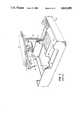
- FIG. 1is an isometric view partially exploded with a portion of the frame section of an electrostatographic reproducing apparatus with a representative illustration of a wiring harness conventionally employed.
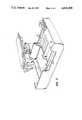
- FIG. 2is a view similar to that illustrated in FIG. 1 wherein the conventional wiring harness has at least in part been replaced by the in situ formed conductive paths according to the present invention.
- FIG. 3is schematic illustration of a system for forming the electrically conductive traces in a structural member.
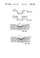
- FIGS. 4A and 4Bare cross-sectional views of a three-dimensional structural member having one electrically conductive path formed therein.
- FIGS. 5A and 5Bare enlarged views of the electrically conductive paths in FIG. 4.
- an electrically conductive pathis formed in a polymer matrix which is filled with electrically insulating fibers that are capable of heat conversion to electrically conducting fibers.
- the conductive pathis obtained by selectively heating the filled polymer matrix to form in situ the electrically conductive path.
- FIGS. 1 and 2the significance of the present invention will be immediately appreciated.
- a structural frame 10 together with machine drive module 12, and platen drive module 14are illustrated as parts of an electrostatographic reproducing apparatus.
- FIG. 1a conventional wiring harness is illustrated comprising a plurality of individual wires 16 held in the harness configuration by fasteners 18 which is here illustrated as a distributing power and/or logic signals from, for example, the control panel on frame 10 to the main machine drive 12.
- FIG. 2illustrates an application of the present invention wherein electro-conductive paths or traces 20 may be formed directly in the machine support frame 10. These electro-conductive paths may be formed as the final step in the manufacture of the individual support frames 20 prior to the assembly of the whole machine and thereby avoid the necessity for manual placement and connection of the conventional wiring harness.
- the electrically insulating polymer matrixmay be formed from any suitable host polymer which is electrically insulating.
- the polymermay be selected from a wide range of commercially available materials which are suitable for molding or other shaping methods such as, for example, casting, extrustion, pultrusion and transfer molding. Polymers which are hydrophobic, exhibiting low moisture uptake are preferred due to their more stable volume resistivity at high relative humidity. Naturally, polymers which are non-toxic and have non-toxic thermal decomposition products are preferred.
- the polymermay for example be selected from a wide range of thermoplastic and thermosetting polymers as well as structural foams of these materials.
- Typical materialsinclude polystyrene, polycarbonate, polyamides, polyesters, phenolics, epoxies, vinyl esters and the like.
- suitable elastomerssuch as for example silicones, urethanes, Hypalons, EPDMs and foams thereof may be used.
- thermoplastic polymersare the ABS resin acrylonitrile-butadiene-styrene copolymer which may be a blend produced from all three monomers or mixtures of copolymers or graft polymers such as styrene and acrylonitrile grafted on polybutadiene.
- polysulfonepolysulfone
- polyphenylene sulfidepolyether imides
- poly(amide-imide)poly(amide-imide)
- fluoroplasticsmay be used.
- low cost molding materialsincluding polyphenylene oxides such as Noryl may be used.
- the electrically insulating polymermay be loaded with any suitable polymeric fibrous material capable of heat conversion to conductive fibrous carbon within the polymer matrix.
- suitable polymeric fibrous materialcapable of heat conversion to conductive fibrous carbon within the polymer matrix.
- Typical of such fibrous fillerare cellulose (rayon) and petroleum pitch based carbon fibers which are heat convertible carbonaceous fibers.
- a particularly preferred carbonaceous fiber of filleris thermally stabilized, polyacrylonitrile fibers which upon heat conversion provide electrically conducting fibers. These fibers are thermally stabilized by heating polyacrylonitrile fibers to temperatures of the order 300° C. in the presence of oxygen and usually under tension for a long period of time of up to twenty four hours wherein the polyacrylonitrile is changed from a white to black fiber while maintaining its electrically insulating characteristics.
- These thermally stabilized fibersalso known as preox fibers can be made electrically conducting upon subsequent heat treatment to temperatures of the order of 2,000° C. in an inert atmosphere.
- the term electrically insulatingis intended to define materials having a resistivity greater than about 10 14 ohm centimeters and the term electrically conductive is intended to define materials having a resistivity less than about 10 9 ohm centimeters.
- the degree of loading the polymer matrix with the fibersis such that upon the heat conversion of the fibers the converted fibers are in electrical contact providing an electrically conducting path in the polymer matrix.
- the fibersmay be included in the polymer matrix in an amount of from about 5 to 70% by weight of the total filled polymer matrix. Preferably, however, from about 10 to 30% by weight of the polymer matrix is made up of the fibers.
- the cost of the fibersis substantially more than the cost of the polymer this range generally provides a good balance between cost and filler function in addition to providing the conducting path.
- the fiberscan have an adhesion promoter such as polyvinyl alcohol, polyvinyl chloride or expoxy monomers coated thereon to enable the polymer in the fluid state when it is heated to readily adhere to the fibers.
- other additivessuch as fiber glass or flame retardents such as halogenated hydrocarbons may be added to the polymer matrix for additional reinforcement and flame retardency respectively.
- the fibershave a length much greater than the diameter with the length being from about 1 to about 12 millimeters and the diameter from about 5 ⁇ 10 -3 to about 5 ⁇ 10 -2 millimeters. It is important that the fibers be of sufficient length that upon pyrolysis they are capable of bridging the area from the pyrolyzed polymer matrix to the bulk of the unpyrolyzed polymer matrix to give durability to the final product. It is therefore important that the fibers maintain their fibrous nature during the compounding operation that result in a uniform dispersion of fibers throughout the polymer matrix. In addition to the fibers providing the conductive path following heat conversion, they also add structure to the host polymer acting to strengthen and stiffen it. In some applications compounding and molding techniques such as 2-shot molding, for example, that cause the fibers to preferentially move to the surface may be preferred.
- the filled polymer matrixmay be formed into an electrical component by conventional molding or extruding techniques.
- a particularly preferred techniqueis injection molding wherein three dimensional parts may be made in a very short time which do not require any post machining such as drilling or routing.
- the electrical componentis to be used as a support member such as the structural frame member or cover the polymer used should be one of the structural polymers mentioned above.
- a portion of the polymer matrix corresponding to the desired conductive pathis heated to a temperature sufficient to convert the electrically insulating fibrous filler to an electrically conductive fibrous filler thereby providing the electrically conductive path.
- the requisite heatingmay be carried out in any suitable manner which generates sufficient thermal excitation in the polymer matrix to convert the electrically insulating fibrous filler to an electrically conductive filler in the desired areas. While other techniques such as electron beam may be used, it is preferred to use a laser beam directed to a portion of the polymer matrix to pyrolyze the portion by melting the polymer and heat convertive the electrically insulating fibers to electrically conductive fibers to form the conductive path.
- a laseris a fast efficient tool and both continuous wave or pulsed laser may be employed which provide a narrow laser beam exposure of the polymer matrix in a predetermined pattern so that the convertible fibers will selectively absorb the radiation and heat convert preferentially becoming conductive over the host polymer.
- any suitable lasermay be employed it being required only that it impinge on the polymer matrix for a sufficient time and with sufficient power to raise the temperature of the fibrous filler to a temperature sufficient to render it electrically conducting. Both argon and carbon dioxide lasers are effective in this regard.
- the polymer matrixis heated locally and undergoes a thermal melting and decomposition with the hottest areas decomposing with the potential for some volatile decomposition products cooling upon contact with and then condensing on adjacent areas. There is some molten plastic flow in a narrow area and a narrow groove or trough may be observed in the exposed areas.
- the fibersare converted to electrically conducting fibers and may be observed in the groove or trough with the heat converted conductive portion of the fiber in the trough and the remaining insulating portion in the unpyrolyzed polymer matrix. As discussed previously, it is important that the fiber fill density be sufficient to insure a plurality of contact points between fibers to produce a continuous conductive fiber path.
- the exposure or heat conversionis preferably carried out in an oxygen free atmosphere since oxygen tends to impede achieving high conductivity by converting carbon to carbon dioxide gas.
- the polymer/fiber compositionhas to be capable of absorbing the laser energy and the product of the absorption must be the necessary rise in temperature to melt or vaporize the polymer and heat convert the fibers.
- the fiber filled polymer matrixmust absorb light at the writing or marking wavelength of the laser and result in the necessary rise in temperature.
- a test plaque made of ABS resin with 30% by weight of heat stabilized chopped preox polyacylonitrile fibers when exposed to a 200 watt peak power industrial CO 2 laser used at 20 watts and pulsed unfocused at 200 to 300 pulses/sec, while scanning at about 1.4 inches/secproduced a visible groove forming a conductive trace in the plaque having a D.C. volume resistivity of about 20 ohm-cm.
- This level of conductivityis sufficient for some purposes such as for example in situations where a high series impedance can be tolerated such as a sensor, for example, or in forming a pattern for subsequent electroplating the trace.
- the conductive pathsmay be individually created by directing a single laser beam for each path. If it is desired to create a plurality of conductive paths in a single piece part, a programmable bed or robot may be coupled in unison with the laser. The motion of the robot would align and carry the part under the laser at a predetermined scan rate. Upon completion of the formation of one conductive path, the laser can be shut off, the part indexed and realigned and the laser re-energized and the bed proceed to once again transport the part under the laser.
- the piece partcan be masked with a mask having a predetermined conductive path pattern and thereafter randomly and/or continuously exposed to the laser thereby pyrolyzing only that portion of the substrate through the pattern in the mask.
- a maskis made from a material which is known to reflect the energy of the laser used.
- a copper maskcould be used to reflect the energy of the carbon dioxide laser without effect upon the copper.
- This procedurehas the advantage in that the pattern size, shape and number of conductive paths are controlled by the mask and not by the programmable bed. Accordingly, higher line densities, better line resolution as well as improved pattern repeatability are achievable. Furthermore, process efficiency can be enhanced with the use of wide laser beams to pyrolyze many traces by a single pass of the part under the laser.
- the laser beamis moved relative to the piece in which it is desired to create a conductive path or a pattern of conductive paths. This may be readily accomplished by holding the laser beam or the work piece stationary while the other is moved relative to the stationary item or by simultaneously moving both the laser and work piece in a controlled programmed manner.
- conductive paths or patterns of conductive pathsmay be readily created in three-dimensional objects or shapes as well as to two-dimensional surfaces.
- FIG. 3schematically illustrates a manner in which a plurality of conductive paths representing circuit patterns can be prepared in a part.
- the part 40is secured to table 42 which is rotatably mounted about the center axis 43 or a motor shaft (not shown) in the motor box 44.
- the tableis movable in the XY plane by movement of worm gear 46 by another motor (not shown) in the motor box 44.
- the laser scanning carriage 48has three lasers 50, 52, 54, one directed in each direction with the carriage movable vertically by worm gear 56 and motor 58 and horizontally by worm gear 60 and motor 62.
- the movement of the table 42 and the scanning carriage 48is controlled by a programmable controller 64 to form the preselected pattern of conductive traces in the part 40.
- a mask 66 having a predetermined patternmaybe placed over at least a portion of the part so that the part may be continuously exposed to the laser. If desired the entire assembly may be placed in an inert atmosphere or a vacuum chamber. Alternatively or in addition an exhaust hose may be placed adjacent the part being marked to remove any noxious materials produced by pyrolysis.
- FIG. 3is merely representative of one manner and device that may be used to form the pattern of conductive traces and that other apparatus and techniques can be used.
- the lasermay be stationary and used with rotating or translating mirrors programmed to cause the beam to scan the part in one, two or three directions.
- the techniques described abovecan be used to provide the necessary circuit in situ in the individual piece parts as frames, covers, support members, etc. so that upon assembly of the final product, the individual piece parts can be put in their proper position and the use of individual wires and wiring harnesses substantially minimized if not eliminated.
- the electrical contacts between the conductive paths on the individual piece partsmay be made with those conventional techniques available to the printed circuit board industry.
- effective techniquesinclude the use of the creation of electrically conductive lands or pads as part of the circuit proper in the individual piece parts which are placed in contact as a result of their final positioning in the main machine thereby completing the circuits.
- a structural component 26such as a subchassis may be made from an insulating structural polymer matrix 27 filled with heat convertible fibers which has a conductive path 28 formed therein.
- the polymer matrixmay be present as an adherent coating 36 on a support member 38 as illustrated in FIG. 4B.
- the enlarged view of FIG. 5Aillustrates a groove 30 formed in the polymer matrix by melting and some decomposition of the polymer locally in response to exposure to the laser beam.
- the troughs or grooves so formedmay be of the order of 0.1 to 5.0 millimeters wide and from about 0.2 to 2.0 millimeters deep.
- conductive fibers 32Contained within the trough are conductive fibers 32 which have been heat converted by exposure to the laser beam. As previously discussed preferably this exposure or conversion takes place in an oxygen-free atmosphere. While the portion 32 of the individual fibers in the trough has been heat converted it should be noted that a portion 34 of the individual fibers extending into the polymer matrix has not been heat converted and serves to anchor the fibers in place in the polymer matrix.
- the groove 30may have an adherent metallic layer 39 plated thereon by conventional techniques to achieve metallic conductivity.
- a carbon dioxide laser with a beam focused to a 200 micron spot having an output power of 1.8 wattswas used to produce traces in a series of 2" ⁇ 2" injection molded test plaques made of polyphenylene oxide, General Electric Noryl resin, with 20% by weight of the total weight being heat stabilized preox polyacrylonitrile fibers chopped to lengths of about 6 mm with diameters of about 10 microns.
- the test plaqueswere placed on a programmable sample table in a vacuum chamber with a transparent window for passages of the continuous wave laser beam and the following traces were made while argon flowed continuously over the samples in the chamber at a pressure of 6 Torr.
- the number of scansis the number of replicate scans in the same trace to try to achieve better uniformity.
- the resistivity for all traceswas determined to be about 0.8 ohm cm.
- Example 4The plaque of Example 4 was placed in a commercial gold electroplating solution (Orotemps-24, a neutral gold plating solution available from Technic Inc., Buffalo, R.I., with 2.4 volts current limited to 1 to 5 milliamps/centimeter for 8 to 12 minutes after which it was removed from the bath rinsed in deionized water and dried. Visual observation confirmed that gold had been electroplated in the trace area.
- the DC resistancewas determined to be near zero with a conventional multimeter.
- Example 1-7Ten parts by weight of the composition which the plaques are made of in Examples 1-7 was mixed with 90 parts of weight of toluence and milled in a roll mill for 48 hours to dissolve the polymer. The resulting despersion was applied with a brush to the surface of a test plaque of unfilled Noryl molded structural foam in a thickness of about 1 mil. Following drying of the coated plaque it was exposed to the laser beam in the manner of Examples 1-7 with a conductive trace being formed. The trace carried into the substrate and the resultant conductive path was formed by the fibers originally in the coating residing eventually in the substrate.
- a carbon dioxide laser with a beam focused to a 200 micron spot having an output power of 3 wattswas used to produce a trace in a 2" ⁇ 2" injection molded test plaque made from General Electric Ultem resin, polyetherimide, filled with 20% by weight of the total weight of heat stabilized preox polyacrylonitrile fibers chopped to a length of about 6 mm with a diameter of about 10 microns.
- the plaquewas placed on a programmable sample table in a vacuum chamber with argon continuously flowing over the sample at a pressure of 8 Torr while a trace was made in the plaque with a single scan of the laser at a scan rate of 1 mm/sec.
- a conductive trace about 0.2 cm wide and 0.4 cm deep with a resistivity of about 2.1 ⁇ 10 -3 ohm cmwas produced.
- Example 10The procedure of Example 10 was repeated except that the plaque was made from General Electric Noryl resin, polyphenylene oxide, filled with 20% by weight of the total weight of the same heat stabilized preox polyacrylonitrile fibers and the scanning rate was 2 mm/sec. A trace having about the same geometry and a resistivity of about 7.4 ⁇ 10 -3 ohms cm was obtained.
- the present inventionprovides an economical alternative to conventional wiring and wire harness construction. It has the advantage of being able to integrate electrical or mechanical functions in the same piece part while at the same time facilitating automated manufacture of individual piece parts and automated assembly of such parts in a machine configuration.
- machine and component circuitryinto mechanical or structural members, substantial cost savings may be achieved in manufacturing and assembly labor, inventory costs in that individual wires, pins, connectors, etc. can be eliminated.
- a typical conventional wiring harness of say 70 wires and connectorscan be reduced to but a single part.
- substantial reduction in manufacturing and assembly error as a result of human involvementmay be avoided.
- the technique according to the present inventionis capable of automated mass production, substantial cost savings may be passed on to the ultimate consumer.
Landscapes
- Engineering & Computer Science (AREA)
- Microelectronics & Electronic Packaging (AREA)
- Manufacturing & Machinery (AREA)
- Chemical & Material Sciences (AREA)
- Organic Chemistry (AREA)
- Electrochemistry (AREA)
- Materials Engineering (AREA)
- Metallurgy (AREA)
- Chemical Kinetics & Catalysis (AREA)
- Manufacturing Of Printed Wiring (AREA)
- Accessory Devices And Overall Control Thereof (AREA)
- Control Or Security For Electrophotography (AREA)
- Compositions Of Macromolecular Compounds (AREA)
- Internal Circuitry In Semiconductor Integrated Circuit Devices (AREA)
- Non-Insulated Conductors (AREA)
- Manufacturing Of Electric Cables (AREA)
Abstract
Description
______________________________________ Example Scan Rate Trace Width Trace Power mm/sec Scans Inches ______________________________________ 1 1.8 W .3 1 0.044-0.060 2 1.8 W .3 2 0.060-0.064 3 1.8 W .6 1 0.056-0.060 4 1.8 W .6 2 0.060-0.064 5 1.8 W 1.0 2 0.036-0.040 6 1.8 W 2.0 2 0.028-0.032 7 1.8 W 3.0 2 0.024-0.028 ______________________________________
Claims (44)
Priority Applications (4)
| Application Number | Priority Date | Filing Date | Title |
|---|---|---|---|
| US07/188,984US4841099A (en) | 1988-05-02 | 1988-05-02 | Electrically insulating polymer matrix with conductive path formed in situ |
| JP1105709AJPH0690884B2 (en) | 1988-05-02 | 1989-04-25 | Electrical device containing an electrically insulating polymer matrix having conductive paths formed in the polymer matrix |
| DE68916318TDE68916318T2 (en) | 1988-05-02 | 1989-04-28 | Electrically insulating plastic matrix with in-situ shaped cables. |
| EP89304345AEP0340997B1 (en) | 1988-05-02 | 1989-04-28 | Electrically insulating polymer matrix with conductive path formed in situ |
Applications Claiming Priority (1)
| Application Number | Priority Date | Filing Date | Title |
|---|---|---|---|
| US07/188,984US4841099A (en) | 1988-05-02 | 1988-05-02 | Electrically insulating polymer matrix with conductive path formed in situ |
Publications (1)
| Publication Number | Publication Date |
|---|---|
| US4841099Atrue US4841099A (en) | 1989-06-20 |
Family
ID=22695408
Family Applications (1)
| Application Number | Title | Priority Date | Filing Date |
|---|---|---|---|
| US07/188,984Expired - LifetimeUS4841099A (en) | 1988-05-02 | 1988-05-02 | Electrically insulating polymer matrix with conductive path formed in situ |
Country Status (4)
| Country | Link |
|---|---|
| US (1) | US4841099A (en) |
| EP (1) | EP0340997B1 (en) |
| JP (1) | JPH0690884B2 (en) |
| DE (1) | DE68916318T2 (en) |
Cited By (51)
| Publication number | Priority date | Publication date | Assignee | Title |
|---|---|---|---|---|
| US4970553A (en)* | 1989-12-04 | 1990-11-13 | Xerox Corporation | Electrical component with conductive path |
| US4985601A (en)* | 1989-05-02 | 1991-01-15 | Hagner George R | Circuit boards with recessed traces |
| US5055637A (en)* | 1989-05-02 | 1991-10-08 | Hagner George R | Circuit boards with recessed traces |
| US5153023A (en)* | 1990-12-03 | 1992-10-06 | Xerox Corporation | Process for catalysis of electroless metal plating on plastic |
| EP0520740A1 (en)* | 1991-06-26 | 1992-12-30 | Xerox Corporation | Electrically connectable module |
| US5267866A (en)* | 1991-12-17 | 1993-12-07 | Xerox Corporation | Flexible electrical interconnect |
| US5270106A (en)* | 1990-04-16 | 1993-12-14 | Xerox Corporation | Fibrillated pultruded electronic component |
| US5281771A (en)* | 1991-12-18 | 1994-01-25 | Xerox Corporation | Multilayer wiring board, interlevel connector, and method for making same |
| US5298681A (en)* | 1992-04-20 | 1994-03-29 | Xerox Corporation | Frame member and assembly for carrying electrical signals and the like |
| US5326935A (en)* | 1992-08-12 | 1994-07-05 | Totoku Electric Co., Ltd. | Multi-layered insulated wire for high frequency transformer winding |
| US5354607A (en)* | 1990-04-16 | 1994-10-11 | Xerox Corporation | Fibrillated pultruded electronic components and static eliminator devices |
| US5362925A (en)* | 1992-08-12 | 1994-11-08 | Totoku Electric Co., Ltd. | Multi-layered insulated wire for high frequency transformer winding |
| US5399424A (en)* | 1992-12-28 | 1995-03-21 | Xerox Corporation | Fibrillated pultruded electronic component |
| US5414216A (en)* | 1993-10-12 | 1995-05-09 | Xerox Corporation | Electrostatographic reproducing machine resistive carbon fiber wire |
| US5420465A (en)* | 1991-12-18 | 1995-05-30 | Xerox Corporation | Switches and sensors utilizing pultrusion contacts |
| US5726482A (en)* | 1994-02-08 | 1998-03-10 | Prolinx Labs Corporation | Device-under-test card for a burn-in board |
| US5767575A (en)* | 1995-10-17 | 1998-06-16 | Prolinx Labs Corporation | Ball grid array structure and method for packaging an integrated circuit chip |
| US5808351A (en)* | 1994-02-08 | 1998-09-15 | Prolinx Labs Corporation | Programmable/reprogramable structure using fuses and antifuses |
| US5834824A (en)* | 1994-02-08 | 1998-11-10 | Prolinx Labs Corporation | Use of conductive particles in a nonconductive body as an integrated circuit antifuse |
| US5872338A (en)* | 1996-04-10 | 1999-02-16 | Prolinx Labs Corporation | Multilayer board having insulating isolation rings |
| US5906042A (en)* | 1995-10-04 | 1999-05-25 | Prolinx Labs Corporation | Method and structure to interconnect traces of two conductive layers in a printed circuit board |
| US5906043A (en)* | 1995-01-18 | 1999-05-25 | Prolinx Labs Corporation | Programmable/reprogrammable structure using fuses and antifuses |
| US5917229A (en)* | 1994-02-08 | 1999-06-29 | Prolinx Labs Corporation | Programmable/reprogrammable printed circuit board using fuse and/or antifuse as interconnect |
| US6034427A (en)* | 1998-01-28 | 2000-03-07 | Prolinx Labs Corporation | Ball grid array structure and method for packaging an integrated circuit chip |
| DE19916467C1 (en)* | 1999-04-12 | 2001-01-11 | Ticona Gmbh | Process for the production of electrically conductive layers on the surface of molded plastic parts by laser energy and the object produced with them |
| US20020040805A1 (en)* | 2000-02-04 | 2002-04-11 | Swager Timothy M. | Insulated nanoscopic pathways, compositions and devices of the same |
| US6417486B1 (en) | 1999-04-12 | 2002-07-09 | Ticona Gmbh | Production of conductor tracks on plastics by means of laser energy |
| US20040029471A1 (en)* | 2000-11-21 | 2004-02-12 | Birgit Severich | Method for graphitising a carbonised fabric |
| US20040189170A1 (en)* | 2001-02-15 | 2004-09-30 | Integral Technologies, Inc. | Low cost lighting circuits manufactured from conductive loaded resin-based materials |
| US20040217472A1 (en)* | 2001-02-16 | 2004-11-04 | Integral Technologies, Inc. | Low cost chip carrier with integrated antenna, heat sink, or EMI shielding functions manufactured from conductive loaded resin-based materials |
| US20050031840A1 (en)* | 2003-08-05 | 2005-02-10 | Xerox Corporation | RF connector |
| US20050029009A1 (en)* | 2003-08-05 | 2005-02-10 | Xerox Corporation | Multi-element connector |
| US20060073607A1 (en)* | 2003-12-05 | 2006-04-06 | Massachusetts Institute Of Technology | Organic materials able to detect analytes |
| US20060127929A1 (en)* | 2004-09-17 | 2006-06-15 | Massachusetts Institute Of Technology | Polymers for analyte detection |
| US20060250781A1 (en)* | 2003-06-27 | 2006-11-09 | Infineon Technologies Ag | Electronic module and method for the production thereof |
| US20080085566A1 (en)* | 2006-10-05 | 2008-04-10 | Massachusetts Institute Of Technology | Emissive compositions with internal standard and related techniques |
| US20100132987A1 (en)* | 2007-03-27 | 2010-06-03 | Nikolaus Hautmann | Method for producing an electrically conductive path on a plastic component |
| US20100168303A1 (en)* | 2004-06-15 | 2010-07-01 | Asahi Kasei Chemicals Corporation | TAB leader tape made of polyphenylene ether-based resin |
| US20110186430A1 (en)* | 2010-02-02 | 2011-08-04 | Matthew Carlyle Sauers | Biosensor and methods for manufacturing |
| US20110212344A1 (en)* | 2010-02-26 | 2011-09-01 | Qing Gong | Metalized Plastic Articles and Methods Thereof |
| US20110274944A1 (en)* | 2010-05-10 | 2011-11-10 | Andri Elia Elia | Polymeric Article Having A Surface Of Different Composition Than Its Bulk And Of Increased Bonding Strength To A Coated Metal Layer |
| US8283423B2 (en) | 2006-09-29 | 2012-10-09 | Massachusetts Institute Of Technology | Polymer synthetic technique |
| CN101682981B (en)* | 2007-05-31 | 2012-12-12 | 罗伯特·博世有限公司 | Control device of a motor vehicle |
| US8367001B2 (en) | 1998-05-05 | 2013-02-05 | Massachusetts Institute Of Technology | Emissive sensors and devices incorporating these sensors |
| US8465678B2 (en) | 1998-05-05 | 2013-06-18 | Massachusetts Institute Of Technology | Emissive polymers and devices incorporating these polymers |
| US8816019B2 (en) | 2013-01-07 | 2014-08-26 | Sabic Global Technologies B.V. | Thermoplastic compositions for laser direct structuring and methods for the manufacture and use thereof |
| US8841000B2 (en) | 2010-08-19 | 2014-09-23 | Byd Company Limited | Metalized plastic articles and methods thereof |
| US8920936B2 (en) | 2010-01-15 | 2014-12-30 | Byd Company Limited | Metalized plastic articles and methods thereof |
| WO2015104651A1 (en) | 2014-01-08 | 2015-07-16 | Global Technology Bridge, Inc. | Apparatus having management of electrical power capacity regions and management of thermal capacity regions |
| US9429522B2 (en) | 2006-10-27 | 2016-08-30 | Massachusetts Institute Of Technology | Sensor of species including toxins and chemical warfare agents |
| WO2025034396A1 (en)* | 2023-08-08 | 2025-02-13 | E Ink Corporation | Backplanes for segmented electro-optic displays and methods of manufacturing same |
Families Citing this family (5)
| Publication number | Priority date | Publication date | Assignee | Title |
|---|---|---|---|---|
| DE10109087A1 (en)* | 2001-02-24 | 2002-10-24 | Leoni Bordnetz Sys Gmbh & Co | Method for producing a molded component with an integrated conductor track |
| DE10132092A1 (en) | 2001-07-05 | 2003-01-23 | Lpkf Laser & Electronics Ag | Track structures and processes for their manufacture |
| CN1326435C (en)* | 2001-07-05 | 2007-07-11 | Lpkf激光和电子股份公司 | Conductor track structures and method for production thereof |
| US7569331B2 (en) | 2005-06-01 | 2009-08-04 | Hewlett-Packard Development Company, L.P. | Conductive patterning |
| US8965159B1 (en) | 2013-11-07 | 2015-02-24 | International Business Machines Corporation | Implementing twisted pair waveguide for electronic substrates |
Citations (21)
| Publication number | Priority date | Publication date | Assignee | Title |
|---|---|---|---|---|
| US3056881A (en)* | 1961-06-07 | 1962-10-02 | United Aircraft Corp | Method of making electrical conductor device |
| US3406126A (en)* | 1966-12-07 | 1968-10-15 | Avco Corp | Conductive synthetic resin composition containing carbon filaments |
| US3414863A (en)* | 1956-05-28 | 1968-12-03 | Jerome H. Lemelson | Electrically conducting panel |
| US3434014A (en)* | 1967-06-13 | 1969-03-18 | Rca Corp | Packaging of electrical equipment |
| US3614541A (en)* | 1969-04-08 | 1971-10-19 | North American Rockwell | Package for an electronic assembly |
| US3626143A (en)* | 1969-04-02 | 1971-12-07 | American Can Co | Scoring of materials with laser energy |
| US3627858A (en)* | 1969-11-24 | 1971-12-14 | Monsanto Res Corp | Method for selectively foaming the surface of a thermoplastic article by use of a laser |
| DE2647796A1 (en)* | 1976-10-22 | 1978-04-27 | Walter Ludwig Zink | PCB acting simultaneously as base of module housing - has wiring in channels separated by raised portions in under side of panel |
| US4159414A (en)* | 1978-04-25 | 1979-06-26 | Massachusetts Institute Of Technology | Method for forming electrically conductive paths |
| US4286250A (en)* | 1979-05-04 | 1981-08-25 | New England Instrument Company | Laser formed resistor elements |
| US4401590A (en)* | 1980-03-26 | 1983-08-30 | Matsushita Electric Industrial Company, Limited | Conductive pyrolytic product and composition using same |
| US4469984A (en)* | 1981-02-13 | 1984-09-04 | Sergeev Jury S | Grid-like electrode for electronic components and process for making same |
| US4489230A (en)* | 1982-02-15 | 1984-12-18 | Alps Electric Co., Ltd. | Manufacturing method for a resistance element |
| US4502098A (en)* | 1981-02-10 | 1985-02-26 | Brown David F | Circuit assembly |
| US4563078A (en)* | 1984-08-31 | 1986-01-07 | Xerox Corporation | Electrostatographic apparatus frame with plural alternative mounting elements |
| US4568632A (en)* | 1982-10-07 | 1986-02-04 | International Business Machines Corporation | Patterning of polyimide films with far ultraviolet light |
| US4584456A (en)* | 1982-09-08 | 1986-04-22 | Tokyo Shibaura Denki Kabushiki Kaisha | Production of resistor from insulating material by local heating |
| US4599193A (en)* | 1983-06-30 | 1986-07-08 | Director-General Of The Agency Of Industrial Science And Technology, An Organ Of The Ministry Of International Trade And Industry Of Japan | Highly electroconductive pyrolyzed product retaining its original shape and composition formed therefrom |
| US4606955A (en)* | 1985-06-18 | 1986-08-19 | E. I. Du Pont De Nemours And Company | Conductive pyrolyzed dielectrics and articles made therefrom |
| US4675467A (en)* | 1986-04-05 | 1987-06-23 | Chronar Corp. | Directed energy conversion of semiconductor materials |
| US4691091A (en)* | 1985-12-31 | 1987-09-01 | At&T Technologies | Direct writing of conductive patterns |
- 1988
- 1988-05-02USUS07/188,984patent/US4841099A/ennot_activeExpired - Lifetime
- 1989
- 1989-04-25JPJP1105709Apatent/JPH0690884B2/ennot_activeExpired - Lifetime
- 1989-04-28DEDE68916318Tpatent/DE68916318T2/ennot_activeExpired - Lifetime
- 1989-04-28EPEP89304345Apatent/EP0340997B1/ennot_activeExpired - Lifetime
Patent Citations (21)
| Publication number | Priority date | Publication date | Assignee | Title |
|---|---|---|---|---|
| US3414863A (en)* | 1956-05-28 | 1968-12-03 | Jerome H. Lemelson | Electrically conducting panel |
| US3056881A (en)* | 1961-06-07 | 1962-10-02 | United Aircraft Corp | Method of making electrical conductor device |
| US3406126A (en)* | 1966-12-07 | 1968-10-15 | Avco Corp | Conductive synthetic resin composition containing carbon filaments |
| US3434014A (en)* | 1967-06-13 | 1969-03-18 | Rca Corp | Packaging of electrical equipment |
| US3626143A (en)* | 1969-04-02 | 1971-12-07 | American Can Co | Scoring of materials with laser energy |
| US3614541A (en)* | 1969-04-08 | 1971-10-19 | North American Rockwell | Package for an electronic assembly |
| US3627858A (en)* | 1969-11-24 | 1971-12-14 | Monsanto Res Corp | Method for selectively foaming the surface of a thermoplastic article by use of a laser |
| DE2647796A1 (en)* | 1976-10-22 | 1978-04-27 | Walter Ludwig Zink | PCB acting simultaneously as base of module housing - has wiring in channels separated by raised portions in under side of panel |
| US4159414A (en)* | 1978-04-25 | 1979-06-26 | Massachusetts Institute Of Technology | Method for forming electrically conductive paths |
| US4286250A (en)* | 1979-05-04 | 1981-08-25 | New England Instrument Company | Laser formed resistor elements |
| US4401590A (en)* | 1980-03-26 | 1983-08-30 | Matsushita Electric Industrial Company, Limited | Conductive pyrolytic product and composition using same |
| US4502098A (en)* | 1981-02-10 | 1985-02-26 | Brown David F | Circuit assembly |
| US4469984A (en)* | 1981-02-13 | 1984-09-04 | Sergeev Jury S | Grid-like electrode for electronic components and process for making same |
| US4489230A (en)* | 1982-02-15 | 1984-12-18 | Alps Electric Co., Ltd. | Manufacturing method for a resistance element |
| US4584456A (en)* | 1982-09-08 | 1986-04-22 | Tokyo Shibaura Denki Kabushiki Kaisha | Production of resistor from insulating material by local heating |
| US4568632A (en)* | 1982-10-07 | 1986-02-04 | International Business Machines Corporation | Patterning of polyimide films with far ultraviolet light |
| US4599193A (en)* | 1983-06-30 | 1986-07-08 | Director-General Of The Agency Of Industrial Science And Technology, An Organ Of The Ministry Of International Trade And Industry Of Japan | Highly electroconductive pyrolyzed product retaining its original shape and composition formed therefrom |
| US4563078A (en)* | 1984-08-31 | 1986-01-07 | Xerox Corporation | Electrostatographic apparatus frame with plural alternative mounting elements |
| US4606955A (en)* | 1985-06-18 | 1986-08-19 | E. I. Du Pont De Nemours And Company | Conductive pyrolyzed dielectrics and articles made therefrom |
| US4691091A (en)* | 1985-12-31 | 1987-09-01 | At&T Technologies | Direct writing of conductive patterns |
| US4675467A (en)* | 1986-04-05 | 1987-06-23 | Chronar Corp. | Directed energy conversion of semiconductor materials |
Non-Patent Citations (8)
| Title |
|---|
| Article "Laser Microchemistry and its Application to Electron-Device Fabrication", by R. M. Osgood, in Annual Review Physics Chemistry, 1983, 34 pp. 77 through 101. |
| Article "Mold Your Own?" by Ganjei et al., in Circuits Mfg. 6/86, pp. 39, 40, 42, 45, 47 and 50. |
| Article Laser Microchemistry and its Application to Electron Device Fabrication , by R. M. Osgood, in Annual Review Physics Chemistry, 1983, 34 pp. 77 through 101.* |
| Article Mold Your Own by Ganjei et al., in Circuits Mfg. 6/86, pp. 39, 40, 42, 45, 47 and 50.* |
| IBM Tech. Disclosure Bulletin, vol 9, No. 11, Apr. 1967, p. 1474, "Metal Plating of Pyrolyzste Circuitry". |
| IBM Tech. Disclosure Bulletin, vol 9, No. 11, Apr. 1967, p. 1474, Metal Plating of Pyrolyzste Circuitry .* |
| Reprinted Article "New Transfer Process Applies 3-D Circuitry to Molded Substrates by Andveiev in Elect. Pkg. & Prod.", 12/84. |
| Reprinted Article New Transfer Process Applies 3 D Circuitry to Molded Substrates by Andveiev in Elect. Pkg. & Prod. , 12/84.* |
Cited By (74)
| Publication number | Priority date | Publication date | Assignee | Title |
|---|---|---|---|---|
| US4985601A (en)* | 1989-05-02 | 1991-01-15 | Hagner George R | Circuit boards with recessed traces |
| US5055637A (en)* | 1989-05-02 | 1991-10-08 | Hagner George R | Circuit boards with recessed traces |
| EP0431334A3 (en)* | 1989-12-04 | 1992-01-15 | Xerox Corporation | Electrical component with conductive path |
| US4970553A (en)* | 1989-12-04 | 1990-11-13 | Xerox Corporation | Electrical component with conductive path |
| US5270106A (en)* | 1990-04-16 | 1993-12-14 | Xerox Corporation | Fibrillated pultruded electronic component |
| US5354607A (en)* | 1990-04-16 | 1994-10-11 | Xerox Corporation | Fibrillated pultruded electronic components and static eliminator devices |
| US5153023A (en)* | 1990-12-03 | 1992-10-06 | Xerox Corporation | Process for catalysis of electroless metal plating on plastic |
| US5220726A (en)* | 1991-06-26 | 1993-06-22 | Xerox Corporation | Method for manufacturing an electrically connectable module |
| US5297969A (en)* | 1991-06-26 | 1994-03-29 | Xerox Corporation | Electrically connectable module with embedded electrical connectors electrically connected to conductive traces |
| EP0520740A1 (en)* | 1991-06-26 | 1992-12-30 | Xerox Corporation | Electrically connectable module |
| US5267866A (en)* | 1991-12-17 | 1993-12-07 | Xerox Corporation | Flexible electrical interconnect |
| US5281771A (en)* | 1991-12-18 | 1994-01-25 | Xerox Corporation | Multilayer wiring board, interlevel connector, and method for making same |
| US5420465A (en)* | 1991-12-18 | 1995-05-30 | Xerox Corporation | Switches and sensors utilizing pultrusion contacts |
| US5298681A (en)* | 1992-04-20 | 1994-03-29 | Xerox Corporation | Frame member and assembly for carrying electrical signals and the like |
| US5326935A (en)* | 1992-08-12 | 1994-07-05 | Totoku Electric Co., Ltd. | Multi-layered insulated wire for high frequency transformer winding |
| US5362925A (en)* | 1992-08-12 | 1994-11-08 | Totoku Electric Co., Ltd. | Multi-layered insulated wire for high frequency transformer winding |
| US5399424A (en)* | 1992-12-28 | 1995-03-21 | Xerox Corporation | Fibrillated pultruded electronic component |
| US5414216A (en)* | 1993-10-12 | 1995-05-09 | Xerox Corporation | Electrostatographic reproducing machine resistive carbon fiber wire |
| US5808351A (en)* | 1994-02-08 | 1998-09-15 | Prolinx Labs Corporation | Programmable/reprogramable structure using fuses and antifuses |
| US5726482A (en)* | 1994-02-08 | 1998-03-10 | Prolinx Labs Corporation | Device-under-test card for a burn-in board |
| US5834824A (en)* | 1994-02-08 | 1998-11-10 | Prolinx Labs Corporation | Use of conductive particles in a nonconductive body as an integrated circuit antifuse |
| US5917229A (en)* | 1994-02-08 | 1999-06-29 | Prolinx Labs Corporation | Programmable/reprogrammable printed circuit board using fuse and/or antifuse as interconnect |
| US5906043A (en)* | 1995-01-18 | 1999-05-25 | Prolinx Labs Corporation | Programmable/reprogrammable structure using fuses and antifuses |
| US5962815A (en)* | 1995-01-18 | 1999-10-05 | Prolinx Labs Corporation | Antifuse interconnect between two conducting layers of a printed circuit board |
| US5906042A (en)* | 1995-10-04 | 1999-05-25 | Prolinx Labs Corporation | Method and structure to interconnect traces of two conductive layers in a printed circuit board |
| US5767575A (en)* | 1995-10-17 | 1998-06-16 | Prolinx Labs Corporation | Ball grid array structure and method for packaging an integrated circuit chip |
| US5872338A (en)* | 1996-04-10 | 1999-02-16 | Prolinx Labs Corporation | Multilayer board having insulating isolation rings |
| US5987744A (en)* | 1996-04-10 | 1999-11-23 | Prolinx Labs Corporation | Method for supporting one or more electronic components |
| US6034427A (en)* | 1998-01-28 | 2000-03-07 | Prolinx Labs Corporation | Ball grid array structure and method for packaging an integrated circuit chip |
| US8465678B2 (en) | 1998-05-05 | 2013-06-18 | Massachusetts Institute Of Technology | Emissive polymers and devices incorporating these polymers |
| US8367001B2 (en) | 1998-05-05 | 2013-02-05 | Massachusetts Institute Of Technology | Emissive sensors and devices incorporating these sensors |
| DE19916467C5 (en)* | 1999-04-12 | 2007-05-16 | Ticona Gmbh | Process for the production of electrically conductive layers on the surface of plastic molded parts by laser energy and the article produced therewith |
| US6417486B1 (en) | 1999-04-12 | 2002-07-09 | Ticona Gmbh | Production of conductor tracks on plastics by means of laser energy |
| US20020110674A1 (en)* | 1999-04-12 | 2002-08-15 | Frank Reil | Production of conductor tracks on plastics by means of laser energy |
| DE19916467C1 (en)* | 1999-04-12 | 2001-01-11 | Ticona Gmbh | Process for the production of electrically conductive layers on the surface of molded plastic parts by laser energy and the object produced with them |
| US20020040805A1 (en)* | 2000-02-04 | 2002-04-11 | Swager Timothy M. | Insulated nanoscopic pathways, compositions and devices of the same |
| US7186355B2 (en)* | 2000-02-04 | 2007-03-06 | Massachusetts Institute Of Technology | Insulated nanoscopic pathways, compositions and devices of the same |
| US20040029471A1 (en)* | 2000-11-21 | 2004-02-12 | Birgit Severich | Method for graphitising a carbonised fabric |
| US7268479B2 (en) | 2001-02-15 | 2007-09-11 | Integral Technologies, Inc. | Low cost lighting circuits manufactured from conductive loaded resin-based materials |
| US20040189170A1 (en)* | 2001-02-15 | 2004-09-30 | Integral Technologies, Inc. | Low cost lighting circuits manufactured from conductive loaded resin-based materials |
| US20040217472A1 (en)* | 2001-02-16 | 2004-11-04 | Integral Technologies, Inc. | Low cost chip carrier with integrated antenna, heat sink, or EMI shielding functions manufactured from conductive loaded resin-based materials |
| US7602614B2 (en) | 2003-06-27 | 2009-10-13 | Infineon Technologies Ag | Electronic module and method for the production thereof |
| US20060250781A1 (en)* | 2003-06-27 | 2006-11-09 | Infineon Technologies Ag | Electronic module and method for the production thereof |
| US20050031840A1 (en)* | 2003-08-05 | 2005-02-10 | Xerox Corporation | RF connector |
| US20050029009A1 (en)* | 2003-08-05 | 2005-02-10 | Xerox Corporation | Multi-element connector |
| US7052763B2 (en) | 2003-08-05 | 2006-05-30 | Xerox Corporation | Multi-element connector |
| US20100310424A1 (en)* | 2003-12-05 | 2010-12-09 | Massachusetts Institute Of Technology | Organic materials able to detect analytes |
| US20060073607A1 (en)* | 2003-12-05 | 2006-04-06 | Massachusetts Institute Of Technology | Organic materials able to detect analytes |
| US8298830B2 (en) | 2003-12-05 | 2012-10-30 | Massachusetts Institute Of Technology | Organic materials able to detect analytes |
| US7759127B2 (en) | 2003-12-05 | 2010-07-20 | Massachusetts Institute Of Technology | Organic materials able to detect analytes |
| US8916633B2 (en)* | 2004-06-15 | 2014-12-23 | Asahi Kasei Chemicals Corporation | TAB leader tape made of polyphenylene ether-based resin |
| US20100168303A1 (en)* | 2004-06-15 | 2010-07-01 | Asahi Kasei Chemicals Corporation | TAB leader tape made of polyphenylene ether-based resin |
| US8617819B2 (en) | 2004-09-17 | 2013-12-31 | Massachusetts Institute Of Technology | Polymers for analyte detection |
| US20060127929A1 (en)* | 2004-09-17 | 2006-06-15 | Massachusetts Institute Of Technology | Polymers for analyte detection |
| US8283423B2 (en) | 2006-09-29 | 2012-10-09 | Massachusetts Institute Of Technology | Polymer synthetic technique |
| US8802447B2 (en) | 2006-10-05 | 2014-08-12 | Massachusetts Institute Of Technology | Emissive compositions with internal standard and related techniques |
| US20080085566A1 (en)* | 2006-10-05 | 2008-04-10 | Massachusetts Institute Of Technology | Emissive compositions with internal standard and related techniques |
| US9429522B2 (en) | 2006-10-27 | 2016-08-30 | Massachusetts Institute Of Technology | Sensor of species including toxins and chemical warfare agents |
| US20100132987A1 (en)* | 2007-03-27 | 2010-06-03 | Nikolaus Hautmann | Method for producing an electrically conductive path on a plastic component |
| CN101682981B (en)* | 2007-05-31 | 2012-12-12 | 罗伯特·博世有限公司 | Control device of a motor vehicle |
| US8920936B2 (en) | 2010-01-15 | 2014-12-30 | Byd Company Limited | Metalized plastic articles and methods thereof |
| US10392708B2 (en) | 2010-01-15 | 2019-08-27 | Byd Company Limited | Metalized plastic articles and methods thereof |
| US9435035B2 (en) | 2010-01-15 | 2016-09-06 | Byd Company Limited | Metalized plastic articles and methods thereof |
| US20110186430A1 (en)* | 2010-02-02 | 2011-08-04 | Matthew Carlyle Sauers | Biosensor and methods for manufacturing |
| US8721850B2 (en) | 2010-02-02 | 2014-05-13 | Roche Diagnostics Operations, Inc. | Biosensor and methods for manufacturing |
| US20110212344A1 (en)* | 2010-02-26 | 2011-09-01 | Qing Gong | Metalized Plastic Articles and Methods Thereof |
| US9103020B2 (en) | 2010-02-26 | 2015-08-11 | Byd Company Limited | Metalized plastic articles and methods thereof |
| US20110274944A1 (en)* | 2010-05-10 | 2011-11-10 | Andri Elia Elia | Polymeric Article Having A Surface Of Different Composition Than Its Bulk And Of Increased Bonding Strength To A Coated Metal Layer |
| US8846151B2 (en) | 2010-08-19 | 2014-09-30 | Byd Company Limited | Metalized plastic articles and methods thereof |
| US8841000B2 (en) | 2010-08-19 | 2014-09-23 | Byd Company Limited | Metalized plastic articles and methods thereof |
| US9770887B2 (en) | 2010-08-19 | 2017-09-26 | Byd Company Limited | Metalized plastic articles and methods thereof |
| US8816019B2 (en) | 2013-01-07 | 2014-08-26 | Sabic Global Technologies B.V. | Thermoplastic compositions for laser direct structuring and methods for the manufacture and use thereof |
| WO2015104651A1 (en) | 2014-01-08 | 2015-07-16 | Global Technology Bridge, Inc. | Apparatus having management of electrical power capacity regions and management of thermal capacity regions |
| WO2025034396A1 (en)* | 2023-08-08 | 2025-02-13 | E Ink Corporation | Backplanes for segmented electro-optic displays and methods of manufacturing same |
Also Published As
| Publication number | Publication date |
|---|---|
| EP0340997B1 (en) | 1994-06-22 |
| DE68916318D1 (en) | 1994-07-28 |
| DE68916318T2 (en) | 1995-01-12 |
| EP0340997A3 (en) | 1989-11-29 |
| JPH0690884B2 (en) | 1994-11-14 |
| JPH0244611A (en) | 1990-02-14 |
| EP0340997A2 (en) | 1989-11-08 |
Similar Documents
| Publication | Publication Date | Title |
|---|---|---|
| US4841099A (en) | Electrically insulating polymer matrix with conductive path formed in situ | |
| US4970553A (en) | Electrical component with conductive path | |
| US5153023A (en) | Process for catalysis of electroless metal plating on plastic | |
| US4691091A (en) | Direct writing of conductive patterns | |
| US4694138A (en) | Method of forming conductor path | |
| US5139862A (en) | Pultruded electronic device | |
| US5396044A (en) | Method of making a fibrillated pultruded electronic component using a laser beam | |
| TWI423750B (en) | Manufacturing method of forming electrical circuit on non-conductive support | |
| US5354607A (en) | Fibrillated pultruded electronic components and static eliminator devices | |
| US5058800A (en) | Method of making electric circuit device | |
| WO1991014015A1 (en) | Method and materials for forming multi-layer circuits by an additive process | |
| JPH05251121A (en) | Multi-layer wiring assembly | |
| KR20030057535A (en) | Methods of manufacturing a printed circuit board shielded against interfering radiation | |
| JP2502039B2 (en) | Method for forming a conductive path on a plastic substrate | |
| US5885683A (en) | Electrical component exhibiting clean laser cut | |
| US5863405A (en) | Process for forming conductive circuit on the surface of molded article | |
| EP0369772B1 (en) | Device for conducting electrical current | |
| KR910001745B1 (en) | Printed circuit board manufacturing method | |
| US7326463B2 (en) | Conductive circuits or cables manufactured from conductive loaded resin-based materials | |
| US6384345B1 (en) | Three dimensional circuit body and method of manufacturing the same | |
| JP2566559B2 (en) | Manufacturing method of printed wiring board | |
| JPH08148809A (en) | Circuit forming method and conductive circuit forming component | |
| US20050199413A1 (en) | Conductive circuits or cables manufactured from conductive loaded resin-based materials | |
| EP0834598A1 (en) | Selective metallization of three dimensional objects | |
| JPH0745914A (en) | Plastic molded product having patterned metal layer |
Legal Events
| Date | Code | Title | Description |
|---|---|---|---|
| AS | Assignment | Owner name:XEROX CORPORATION, STAMFORD, CT. A CORP. OF N.Y. Free format text:ASSIGNMENT OF ASSIGNORS INTEREST.;ASSIGNOR:EPSTEIN, ARTHUR J.;REEL/FRAME:004893/0480 Effective date:19880415 Owner name:XEROX CORPORATON, STAMFORD, COUNTY OF FAIRFIELD, C Free format text:ASSIGNMENT OF ASSIGNORS INTEREST.;ASSIGNORS:EPSTEIN, ARTHUR J.;EWING, JOAN R.;SWIFT, JOSEPH A.;REEL/FRAME:004893/0481 Effective date:19880426 Owner name:XEROX CORPORATION, CONNECTICUT Free format text:ASSIGNMENT OF ASSIGNORS INTEREST;ASSIGNOR:EPSTEIN, ARTHUR J.;REEL/FRAME:004893/0480 Effective date:19880415 Owner name:XEROX CORPORATON, CONNECTICUT Free format text:ASSIGNMENT OF ASSIGNORS INTEREST;ASSIGNORS:EPSTEIN, ARTHUR J.;EWING, JOAN R.;SWIFT, JOSEPH A.;REEL/FRAME:004893/0481 Effective date:19880426 | |
| STCF | Information on status: patent grant | Free format text:PATENTED CASE | |
| FPAY | Fee payment | Year of fee payment:4 | |
| FPAY | Fee payment | Year of fee payment:8 | |
| FPAY | Fee payment | Year of fee payment:12 | |
| AS | Assignment | Owner name:BANK ONE, NA, AS ADMINISTRATIVE AGENT, ILLINOIS Free format text:SECURITY INTEREST;ASSIGNOR:XEROX CORPORATION;REEL/FRAME:013153/0001 Effective date:20020621 | |
| AS | Assignment | Owner name:JPMORGAN CHASE BANK, AS COLLATERAL AGENT, TEXAS Free format text:SECURITY AGREEMENT;ASSIGNOR:XEROX CORPORATION;REEL/FRAME:015134/0476 Effective date:20030625 Owner name:JPMORGAN CHASE BANK, AS COLLATERAL AGENT,TEXAS Free format text:SECURITY AGREEMENT;ASSIGNOR:XEROX CORPORATION;REEL/FRAME:015134/0476 Effective date:20030625 | |
| AS | Assignment | Owner name:XEROX CORPORATION, CONNECTICUT Free format text:RELEASE BY SECURED PARTY;ASSIGNOR:JPMORGAN CHASE BANK, N.A. AS SUCCESSOR-IN-INTEREST ADMINISTRATIVE AGENT AND COLLATERAL AGENT TO JPMORGAN CHASE BANK;REEL/FRAME:066728/0193 Effective date:20220822 |