US4840757A - Replicating process for interference patterns - Google Patents
Replicating process for interference patternsDownload PDFInfo
- Publication number
- US4840757A US4840757AUS07/051,891US5189187AUS4840757AUS 4840757 AUS4840757 AUS 4840757AUS 5189187 AUS5189187 AUS 5189187AUS 4840757 AUS4840757 AUS 4840757A
- Authority
- US
- United States
- Prior art keywords
- coating
- film
- replicating
- pattern
- patterns
- Prior art date
- Legal status (The legal status is an assumption and is not a legal conclusion. Google has not performed a legal analysis and makes no representation as to the accuracy of the status listed.)
- Expired - Lifetime
Links
- 230000003362replicative effectEffects0.000titleclaimsabstractdescription30
- 238000000034methodMethods0.000titleclaimsdescription27
- 238000000576coating methodMethods0.000claimsabstractdescription64
- 239000011248coating agentSubstances0.000claimsabstractdescription55
- 230000005855radiationEffects0.000claimsabstractdescription27
- 239000000758substrateSubstances0.000claimsabstractdescription16
- 239000000463materialSubstances0.000claimsabstractdescription15
- 239000002985plastic filmSubstances0.000claimsdescription19
- 229920006255plastic filmPolymers0.000claimsdescription15
- 239000000203mixtureSubstances0.000claimsdescription7
- 238000010924continuous productionMethods0.000abstractdescription4
- 239000008199coating compositionSubstances0.000abstractdescription3
- 239000000047productSubstances0.000description13
- 238000010894electron beam technologyMethods0.000description12
- 230000010076replicationEffects0.000description11
- 229920006267polyester filmPolymers0.000description9
- 238000001723curingMethods0.000description5
- 238000005266castingMethods0.000description4
- 239000002131composite materialSubstances0.000description4
- 238000002360preparation methodMethods0.000description4
- 229920005989resinPolymers0.000description4
- 239000011347resinSubstances0.000description4
- 239000004820Pressure-sensitive adhesiveSubstances0.000description3
- VYPSYNLAJGMNEJ-UHFFFAOYSA-NSilicium dioxideChemical compoundO=[Si]=OVYPSYNLAJGMNEJ-UHFFFAOYSA-N0.000description3
- 229920006266Vinyl filmPolymers0.000description3
- 238000004519manufacturing processMethods0.000description3
- 229910052751metalInorganic materials0.000description3
- 239000002184metalSubstances0.000description3
- 229920002120photoresistant polymerPolymers0.000description3
- 239000004800polyvinyl chlorideSubstances0.000description3
- 229920000915polyvinyl chloridePolymers0.000description3
- 238000003825pressingMethods0.000description3
- 229920001169thermoplasticPolymers0.000description3
- 239000004416thermosoftening plasticSubstances0.000description3
- 238000012546transferMethods0.000description3
- SMZOUWXMTYCWNB-UHFFFAOYSA-N2-(2-methoxy-5-methylphenyl)ethanamineChemical compoundCOC1=CC=C(C)C=C1CCNSMZOUWXMTYCWNB-UHFFFAOYSA-N0.000description2
- LVGFPWDANALGOY-UHFFFAOYSA-N8-methylnonyl prop-2-enoateChemical compoundCC(C)CCCCCCCOC(=O)C=CLVGFPWDANALGOY-UHFFFAOYSA-N0.000description2
- 229920001944PlastisolPolymers0.000description2
- 238000001227electron beam curingMethods0.000description2
- 238000004049embossingMethods0.000description2
- 239000012530fluidSubstances0.000description2
- 238000001093holographyMethods0.000description2
- -1hydroxyalkyl acrylateChemical compound0.000description2
- 239000000178monomerSubstances0.000description2
- 125000000962organic groupChemical group0.000description2
- 239000000049pigmentSubstances0.000description2
- 229920003023plasticPolymers0.000description2
- 239000004033plasticSubstances0.000description2
- 239000004999plastisolSubstances0.000description2
- 229920001296polysiloxanePolymers0.000description2
- 238000003847radiation curingMethods0.000description2
- NIXOWILDQLNWCW-UHFFFAOYSA-N2-Propenoic acidNatural productsOC(=O)C=CNIXOWILDQLNWCW-UHFFFAOYSA-N0.000description1
- NIXOWILDQLNWCW-UHFFFAOYSA-MAcrylateChemical compound[O-]C(=O)C=CNIXOWILDQLNWCW-UHFFFAOYSA-M0.000description1
- 239000004925Acrylic resinSubstances0.000description1
- 229920000178Acrylic resinPolymers0.000description1
- 239000004593EpoxySubstances0.000description1
- 239000005909KieselgurSubstances0.000description1
- 229920000877Melamine resinPolymers0.000description1
- CERQOIWHTDAKMF-UHFFFAOYSA-MMethacrylateChemical compoundCC(=C)C([O-])=OCERQOIWHTDAKMF-UHFFFAOYSA-M0.000description1
- CERQOIWHTDAKMF-UHFFFAOYSA-NMethacrylic acidChemical compoundCC(=C)C(O)=OCERQOIWHTDAKMF-UHFFFAOYSA-N0.000description1
- BLRPTPMANUNPDV-UHFFFAOYSA-NSilaneChemical compound[SiH4]BLRPTPMANUNPDV-UHFFFAOYSA-N0.000description1
- 229920002472StarchPolymers0.000description1
- ZJCCRDAZUWHFQH-UHFFFAOYSA-NTrimethylolpropaneChemical compoundCCC(CO)(CO)COZJCCRDAZUWHFQH-UHFFFAOYSA-N0.000description1
- DAKWPKUUDNSNPN-UHFFFAOYSA-NTrimethylolpropane triacrylateChemical compoundC=CC(=O)OCC(CC)(COC(=O)C=C)COC(=O)C=CDAKWPKUUDNSNPN-UHFFFAOYSA-N0.000description1
- 229920006397acrylic thermoplasticPolymers0.000description1
- 239000000853adhesiveSubstances0.000description1
- 230000001070adhesive effectEffects0.000description1
- 229910052782aluminiumInorganic materials0.000description1
- XAGFODPZIPBFFR-UHFFFAOYSA-NaluminiumChemical compound[Al]XAGFODPZIPBFFR-UHFFFAOYSA-N0.000description1
- 150000008064anhydridesChemical class0.000description1
- QVGXLLKOCUKJST-UHFFFAOYSA-Natomic oxygenChemical compound[O]QVGXLLKOCUKJST-UHFFFAOYSA-N0.000description1
- 239000011230binding agentSubstances0.000description1
- 239000004927claySubstances0.000description1
- 238000007596consolidation processMethods0.000description1
- 239000003085diluting agentSubstances0.000description1
- 239000000839emulsionSubstances0.000description1
- 239000003822epoxy resinSubstances0.000description1
- 239000000945fillerSubstances0.000description1
- 239000012467final productSubstances0.000description1
- IVJISJACKSSFGE-UHFFFAOYSA-Nformaldehyde;1,3,5-triazine-2,4,6-triamineChemical compoundO=C.NC1=NC(N)=NC(N)=N1IVJISJACKSSFGE-UHFFFAOYSA-N0.000description1
- VOZRXNHHFUQHIL-UHFFFAOYSA-Nglycidyl methacrylateChemical compoundCC(=C)C(=O)OCC1CO1VOZRXNHHFUQHIL-UHFFFAOYSA-N0.000description1
- 210000000569greater omentumAnatomy0.000description1
- LNEPOXFFQSENCJ-UHFFFAOYSA-NhaloperidolChemical compoundC1CC(O)(C=2C=CC(Cl)=CC=2)CCN1CCCC(=O)C1=CC=C(F)C=C1LNEPOXFFQSENCJ-UHFFFAOYSA-N0.000description1
- 239000012948isocyanateSubstances0.000description1
- 150000002513isocyanatesChemical class0.000description1
- 239000002650laminated plasticSubstances0.000description1
- 238000010030laminatingMethods0.000description1
- 238000011031large-scale manufacturing processMethods0.000description1
- 239000010985leatherSubstances0.000description1
- 238000005259measurementMethods0.000description1
- 239000013528metallic particleSubstances0.000description1
- 239000012299nitrogen atmosphereSubstances0.000description1
- 239000001301oxygenSubstances0.000description1
- 229910052760oxygenInorganic materials0.000description1
- 239000006223plastic coatingSubstances0.000description1
- 229920003229poly(methyl methacrylate)Polymers0.000description1
- 229920000647polyepoxidePolymers0.000description1
- 229920000728polyesterPolymers0.000description1
- 230000003252repetitive effectEffects0.000description1
- 239000000377silicon dioxideSubstances0.000description1
- 239000007787solidSubstances0.000description1
- 239000008107starchSubstances0.000description1
- 235000019698starchNutrition0.000description1
- ISXSCDLOGDJUNJ-UHFFFAOYSA-Ntert-butyl prop-2-enoateChemical compoundCC(C)(C)OC(=O)C=CISXSCDLOGDJUNJ-UHFFFAOYSA-N0.000description1
- 239000012815thermoplastic materialSubstances0.000description1
- 229920006163vinyl copolymerPolymers0.000description1
- 230000004304visual acuityEffects0.000description1
- 230000000007visual effectEffects0.000description1
- 239000002023woodSubstances0.000description1
Images
Classifications
- B—PERFORMING OPERATIONS; TRANSPORTING
- B29—WORKING OF PLASTICS; WORKING OF SUBSTANCES IN A PLASTIC STATE IN GENERAL
- B29C—SHAPING OR JOINING OF PLASTICS; SHAPING OF MATERIAL IN A PLASTIC STATE, NOT OTHERWISE PROVIDED FOR; AFTER-TREATMENT OF THE SHAPED PRODUCTS, e.g. REPAIRING
- B29C37/00—Component parts, details, accessories or auxiliary operations, not covered by group B29C33/00 or B29C35/00
- B29C37/0053—Moulding articles characterised by the shape of the surface, e.g. ribs, high polish
- B—PERFORMING OPERATIONS; TRANSPORTING
- B29—WORKING OF PLASTICS; WORKING OF SUBSTANCES IN A PLASTIC STATE IN GENERAL
- B29C—SHAPING OR JOINING OF PLASTICS; SHAPING OF MATERIAL IN A PLASTIC STATE, NOT OTHERWISE PROVIDED FOR; AFTER-TREATMENT OF THE SHAPED PRODUCTS, e.g. REPAIRING
- B29C41/00—Shaping by coating a mould, core or other substrate, i.e. by depositing material and stripping-off the shaped article; Apparatus therefor
- B29C41/24—Shaping by coating a mould, core or other substrate, i.e. by depositing material and stripping-off the shaped article; Apparatus therefor for making articles of indefinite length
- G—PHYSICS
- G03—PHOTOGRAPHY; CINEMATOGRAPHY; ANALOGOUS TECHNIQUES USING WAVES OTHER THAN OPTICAL WAVES; ELECTROGRAPHY; HOLOGRAPHY
- G03F—PHOTOMECHANICAL PRODUCTION OF TEXTURED OR PATTERNED SURFACES, e.g. FOR PRINTING, FOR PROCESSING OF SEMICONDUCTOR DEVICES; MATERIALS THEREFOR; ORIGINALS THEREFOR; APPARATUS SPECIALLY ADAPTED THEREFOR
- G03F7/00—Photomechanical, e.g. photolithographic, production of textured or patterned surfaces, e.g. printing surfaces; Materials therefor, e.g. comprising photoresists; Apparatus specially adapted therefor
- G03F7/0005—Production of optical devices or components in so far as characterised by the lithographic processes or materials used therefor
- G03F7/001—Phase modulating patterns, e.g. refractive index patterns
- B—PERFORMING OPERATIONS; TRANSPORTING
- B29—WORKING OF PLASTICS; WORKING OF SUBSTANCES IN A PLASTIC STATE IN GENERAL
- B29C—SHAPING OR JOINING OF PLASTICS; SHAPING OF MATERIAL IN A PLASTIC STATE, NOT OTHERWISE PROVIDED FOR; AFTER-TREATMENT OF THE SHAPED PRODUCTS, e.g. REPAIRING
- B29C33/00—Moulds or cores; Details thereof or accessories therefor
- B29C33/56—Coatings, e.g. enameled or galvanised; Releasing, lubricating or separating agents
- B29C33/60—Releasing, lubricating or separating agents
- B—PERFORMING OPERATIONS; TRANSPORTING
- B29—WORKING OF PLASTICS; WORKING OF SUBSTANCES IN A PLASTIC STATE IN GENERAL
- B29C—SHAPING OR JOINING OF PLASTICS; SHAPING OF MATERIAL IN A PLASTIC STATE, NOT OTHERWISE PROVIDED FOR; AFTER-TREATMENT OF THE SHAPED PRODUCTS, e.g. REPAIRING
- B29C35/00—Heating, cooling or curing, e.g. crosslinking or vulcanising; Apparatus therefor
- B29C35/02—Heating or curing, e.g. crosslinking or vulcanizing during moulding, e.g. in a mould
- B29C35/08—Heating or curing, e.g. crosslinking or vulcanizing during moulding, e.g. in a mould by wave energy or particle radiation
- B—PERFORMING OPERATIONS; TRANSPORTING
- B29—WORKING OF PLASTICS; WORKING OF SUBSTANCES IN A PLASTIC STATE IN GENERAL
- B29L—INDEXING SCHEME ASSOCIATED WITH SUBCLASS B29C, RELATING TO PARTICULAR ARTICLES
- B29L2011/00—Optical elements, e.g. lenses, prisms
- Y—GENERAL TAGGING OF NEW TECHNOLOGICAL DEVELOPMENTS; GENERAL TAGGING OF CROSS-SECTIONAL TECHNOLOGIES SPANNING OVER SEVERAL SECTIONS OF THE IPC; TECHNICAL SUBJECTS COVERED BY FORMER USPC CROSS-REFERENCE ART COLLECTIONS [XRACs] AND DIGESTS
- Y10—TECHNICAL SUBJECTS COVERED BY FORMER USPC
- Y10T—TECHNICAL SUBJECTS COVERED BY FORMER US CLASSIFICATION
- Y10T156/00—Adhesive bonding and miscellaneous chemical manufacture
- Y10T156/10—Methods of surface bonding and/or assembly therefor
- Y10T156/1002—Methods of surface bonding and/or assembly therefor with permanent bending or reshaping or surface deformation of self sustaining lamina
- Y10T156/1007—Running or continuous length work
- Y10T156/1023—Surface deformation only [e.g., embossing]
- Y—GENERAL TAGGING OF NEW TECHNOLOGICAL DEVELOPMENTS; GENERAL TAGGING OF CROSS-SECTIONAL TECHNOLOGIES SPANNING OVER SEVERAL SECTIONS OF THE IPC; TECHNICAL SUBJECTS COVERED BY FORMER USPC CROSS-REFERENCE ART COLLECTIONS [XRACs] AND DIGESTS
- Y10—TECHNICAL SUBJECTS COVERED BY FORMER USPC
- Y10T—TECHNICAL SUBJECTS COVERED BY FORMER US CLASSIFICATION
- Y10T156/00—Adhesive bonding and miscellaneous chemical manufacture
- Y10T156/10—Methods of surface bonding and/or assembly therefor
- Y10T156/1002—Methods of surface bonding and/or assembly therefor with permanent bending or reshaping or surface deformation of self sustaining lamina
- Y10T156/1039—Surface deformation only of sandwich or lamina [e.g., embossed panels]
Definitions
- the present inventionrelates to a process for replicating patterns in curable coatings.
- the patternsare characterized by the fact that the dimensions of the patterns are at or below the visible wave length of light. These patterns are generally referred to as interference patterns and typical of these patterns are those commonly known as holographic information patterns and diffraction gratings.
- a radiation curable compositionis coated on a substrate and pressed against the surface bearing the pattern to be reproduced.
- the curable coatingis irradiated to at least cure the coating sufficiently so that it can be removed from the pattern surface and with the pattern replicated in the coating.
- Holographyis a fairly new technology. It was discovered about forty years ago and only in the past ten years have commercial applications appeared. Very simply described holography is the recording of a wave or wave front. It is a technical process for forming a visual record of an object wherein the image produced is three dimensional and appears as solid as the original object.
- hologramsThere are several types of holograms but the main interest of the present invention is in the phase type embossed holograms of which one commonly known type is called a white light hologram.
- One known method of preparing a master phase embossed holograminvolves the following steps:
- the mastercan now be used to impress the interference pattern into plastic for large scale production of reflection holograms. This is commonly done by what is known as the hot stamp process.
- a thermoplastic deformable plastic film that has been first metallizedis placed in contact with the pattern surface of the master hologram.
- the compositeis pressed or stamped together while heat is used to soften the plastic so that it deforms sufficiently to the interference pattern.
- the two layersare then separated with the interference pattern in the plastic film.
- the metallic coatingfunctions like a mirror and reflects white light waves through the interference pattern to create the changing images of the pattern.
- the hot stamp process for replicationis the process most commonly used, it suffers from several serious disadvantages.
- the first disadvantagerelates to the materials involved.
- a requisite for the processis a deformable plastic film of the thermoplastic type.
- the heat usedmust be carefully controlled. If not enough heat is used, the plastic film will not deform. If the heat is excessive, the image will be "flowed away.” Even when replicating conditions are carefully controlled, the thermal stability of the resultant reproduction must be considered. This reproduction is still thermoplastic and can be again deformed if subjected to excessive heat.
- Non-thermoplastic materialswhich could provide many desirable properties to the finished product cannot be utilized in the hot stamping process.
- the hot stamp processrequires uniform heat and pressure in its operation as opposed to endless belts and casting drums.
- a composite of the holographic master and the plastic filmare placed in a press having at least one heated platen.
- the pressis closed for a sufficient period of time to deform the plastic film.
- the pressis opened and the composite is separated.
- the operationis limited to the size of the press.
- the size of the final hologramdetermines the number of hologram images that can be set in place on the hologram master.
- endless belts and casting drumsoffer the opportunity for a continuous replication process.
- masters on the belts and drumsare contacted with the plastic film that receive the image by means of a pressure roll which forms a nip with the belt or roll to join the two materials together.
- the hot stamp processis an embossing process that deforms the plastic coating.
- an embossing processdoes not give 100% replication of patterns, especially the ultrafine patterns such as those with which the present invention is concerned.
- U.S. Pat. Nos. 4,289,821 and 4,322,450describe processes for the manufacture of release coated webs.
- a webis coated with an electron beam curable coating which when cured has release properties.
- the freshly coated webis brought in contact with a continuous replicating surface and while in contact the web is irradiated on its back surface by an electron beam to cure the coating. Once the coating is cured it can be removed from the replicating surface and the pattern of the surface is replicated in the coating.
- Patterns made by the processes of these patentsare leather and wood grain patterns as well as very uniform patterns which provide satin and low gloss finishes. Patterns such as these on the replicating surfaces and on the surfaces of replicated products are identifiable as peaks and valleys and they are measurable.
- a Surtronic 3P profiling instrumentUsing a Surtronic 3P profiling instrument, a set of 7 different patterns, representative of finer replications made by this process, was measured.
- the instrumentwas adapted with a data acquisition interface and related software to generate the average spacing between peaks and the average vertical distance between peaks and valleys.
- the instrumentwas adjusted to filter out any part of the patterns with a wave length of 250 microns or greater.
- the peak to peak averagewas from 7.5 microns to 27.5 microns.
- the peak to valley average vertical distancewas from 2.1 microns to 39.6 microns, far greater than the wave length of visible light.
- the patterns reproducedwill exhibit the same light wave characteristics as the original. For example, if the original provides three dimensional holographic images, the reproduction will also. It is surprising that this degree of reproducibility could be obtained for such small patterns.
- the radiation curable coatingscan be applied to substrates or can be cast as self-supporting films.
- the radiation cured coatingsmay have release properties and the patterns replicated therein can themselves be used for transferring the same pattern to films and decorative laminates by known casting and laminating processes.
- Other well known usesinclude heat transferring printed designs against receptive surfaces (e.g. T-shirts) and the manufacture of pressure sensitive adhesive webs for labels and decals.
- substrateswhich are preferably sheet-like materials such as paper and plastic film, are coated on one side with a radiation curable coating.
- This coated surfacewhile still conformable is then pressed against a replicating surface bearing a light wave interference pattern of a size that is at or below the visible wave length of light to cause the surface of the coating to conform to the interference pattern surface.
- the compositeis irradiated at least sufficiently to set the curable resin and then removed from the replicating surface with the cured resin attached to the substrate.
- the substrate with the cured resin coatinghas a virtually 100% replication of the replicating pattern.
- the radiation curable coatingmay be applied to a temporary carrier or directly onto the replicating surface. After irradiation, the cured coating is a self-supporting, patterned film and is separated from the temporary carrier.
- Any number of radiation curable coating compositionsmay be used. Especially suitable are compositions such as those described in U.S. Pat. Nos. 4,327,121 and 4,311,766.
- the from of radiaton employedis preferably electron beam or ultraviolet light.
- the replicating surfaceis preferably provided by a continuous surface such as an endless belt, roll, drum, or other cylindrical surface, which can be revolved past a radiation curing device.
- the coatingis preferably applied directly to the substrate, before it engages the continuous surface, but can also be applied directly to the replicating surface.
- the replicating surfaceis preferably a metal roll with the pattern directly replicated on its surface but can take other forms such as a plate or sleeve attached to the roll surface.
- the inventionis also the products produced by the above processes.
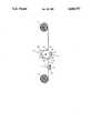
- the FIGUREillustrates schematically the preferred apparatus for carrying out the present invention.
- the FIGUREshows both a substrate and a replicating roll being coated with an electron beam curable composition, after which the substrate, coating and roll are revolved together past an electron beam curing station where the coating is cured, and then the substrate with the cured coating adhered to it, is stripped from the roll.
- coatingis preferably applied either to the substrate or to the replicating roll, but not both.
- a roll 1 of plastic filmis unwound and passed through the following: a coating station 2, and an electron beam curing station 3, from where it is wound onto roll 7.
- the FIGUREalso shows alternative coating station 4.
- the coating station 2is provided by coating roll 10 and backup roll 11 positioned to form a nip through which the film 8 passes.
- Coating roll 10rotates through reservoir 12 of the coating material and transfers a predetermined layer of coating material to one side of film 8.
- Alternative coating station 4is provided by coating roll 13 mounted for rotation in reservoir 14 of coating material and against replicating roll 22.
- the coating roll 13transfers a predetermined layer of coating material to the replicating roll 22.
- the coating station 4would be used when it is desirable to make a self supporting cured film from the radiation curable coating. In such an event, coating material would be applied directly to replicating roll 22.
- the film 8would preferably be replaced by a temporary carrier which would support the coating through the curing operation and could be readily stripped from the cured film at a convenient location.
- coating apparatusis preferred, but any of the conventional coating apparatus, such as knife-over-roll, offset gravure, reverse roll, etc. can be used.
- the replicative surfaceis provided by roll 22, in which the desired pattern is electroformed on the surface.
- the film 8is pressed against the roll 22 by press roll 18 to assure that the coating fills the depressions in the electroformed surface of the roll 22 and that there is continuous intimate contact with the film.
- the roll 22is mounted for rotation by conventional drive means (not shown) and continuously carries the film and coating past the electron beam radiation unit 20 which irradiates the coating and cures it at least sufficiently to permit it to be removed from the roll 22 at take-off roll 19, securely attached to the film 9, and to assure permanent replication of the desired surface.
- Electron beam radiation units useful in the present inventionare readily available and typically consist of a transformer capable of stepping up line voltage and an electron accelerator.
- the electronsare generated from a point source filament and then scanned electromagnetically like a television set to traverse the coated object.
- the electronsare generated in a curtain from an extended filament which can irradiate the entire width of the surface without the need for scanning.
- commercial machinesare available with accelerating voltages of over a million electron volts, the range for this and similar coating applications is typically from 150-300 KV (kiloelectron volts). It is common when curing coatings with electron beam radiation units to take steps to eliminate oxygen from the surface of the coating.
- a nitrogen atmosphereis preferably applied through nozzle 21.
- Typical resins useful in electron beam curable coatingsare styrented polyesters and acrylics, such as vinyl copolymers of various monomers and glycidyl methacrylate reacted with acrylic acid, isocyanate prepolymers reacted with an hydroxyalkyl acrylate, epoxy resins reacted with acrylic or methacrylic acid, and hydroxyalkyl acrylate reacted with an anhydride and subsequently reacted with an epoxy.
- Coating compositions which can be cured by electron beam radiation and are suitable for release functionsgenerally include some or all of the following:
- a reactive monomer diluentsuch as trimethylolpropane triacylate or isodecyl acrylate;
- pigments or fillerssuch as clay, silica or diatomaceous earth
- a holographic master of the type that is conventionally used for hot stamp replicatingwas adhesively attached to the surface of a revolving drum such as that shown in the FIGURE.
- a polyester film of 4 mil thickness and pretreated for adhesionwas coated with a radiation curable coating having the following composition:
- Trimethylolpropane Triacrylate8 parts, by Weight
- An organo functional silicone fluidwas added to the coating in an amount of 2% based on the total coating weight for improving release of a plastic film or sheet later formed against the product produced in this example.
- the coated filmwas pressed against the revolving drum and exposed to electron beam radiation at 4 megarads dosage. The speed of the operation was 150 fpm. After curing, the film was examined for pattern replication. The pattern master was replicated faithfully on the film numerous times at repetitive intervals equal to the circumference of the revolving drum.
- samples of the holographic master die and the patterned and cured polyester filmwere prepared for viewing topographically and in cross-section by a scanning electron microscope.
- the sampleswere viewed at 10,000 ⁇ magnification and photographed.
- the peaks and valleys of the patternswere very identifiable in the photographs.
- the distance from peak to peakwas measured at less than 1 micron (about 0.75 micron).
- the vertical distance from peak to valley on the average for both sampleswas also less than 1 micron (about 0.5 micron) and less than that for peak to peak.
- the visible wave length of lightis from 4,000 angstroms to 7,000 angstroms.
- One micronis equal to 10,000 angstroms.
- the holographic image seen in the replicated film patternshowed the same three dimensional characterists as the holographic image shown in the holographic master.
- Example 2This example is similar in all respects to Example 1 except that a paper web that had been conventionally starch sized and coated with pigment and binder was used in place of polyester film.
- a polyvinyl chloride plastisolwas cast on both the patterned polyester film product of Example 1 and the patterned paper product of Example 2.
- a Gardner metering knifewas used to set down a wet film of 8 mils thickness.
- the plastisolwas dried for 3 minutes at 100° C. and cured for 2 minutes at 190° C.
- the cast polyvinyl chloride filmreadily stripped from both the paper sample and the polyester film sample as a self-supporting film.
- the holographic patternwas faithfully replicated in the polyvinyl chloride film cast from the paper sample and the polyester film sample.
- Example 1the patterned and cured products of Examples 1 and 2 were used as the release sheets to press decorative laminates.
- a 12 by 12 inch platen press at 280° F. and 1200 psiwas used for pressing for 10 minutes.
- the configuration of the stack of materials in the presswas from top to bottom:
- One product of the inventionis a release sheet suitable for heat transferring printed designs to receptive surfaces such as T-shirts and other articles of clothing.
- the release sheetcomprises a substrate having on at least one side thereof a coating of a radiation curable composition which has been cured by radiation.
- the outer surface of the coatinghas a light wave interference pattern at or below the visible wave length of light formed by curing the coating while in contact with a replicating surface having the interference pattern.
- a pressure sensitive adhesive coated webthat is a sheet material with an adhesive coat and a release liner sheet.
- the sheet materialcomprises a substrate having on at least one side thereof a coating of a radiation curable composition which has been cured by radiation.
- the outer surface of the coatinghas a light wave interference pattern at or below the visible wave length of light formed by curing the coating while in contact with a replicating surface having the interference pattern.
- the sheet materialhas the same pattern in it as the replicating surface and the pressure sensitive adhesive web can be converted by known means to produce items such as labels, tapes and decals.
Landscapes
- Physics & Mathematics (AREA)
- General Physics & Mathematics (AREA)
- Engineering & Computer Science (AREA)
- Mechanical Engineering (AREA)
- Holo Graphy (AREA)
Abstract
Description
Claims (1)
Priority Applications (4)
| Application Number | Priority Date | Filing Date | Title |
|---|---|---|---|
| US07/051,891US4840757A (en) | 1987-05-19 | 1987-05-19 | Replicating process for interference patterns |
| PCT/US1988/001554WO1988009252A1 (en) | 1987-05-19 | 1988-05-11 | Replicating process for interference patterns |
| EP19880904875EP0316407A4 (en) | 1987-05-19 | 1988-05-11 | Replicating process for interference patterns |
| CA000567028ACA1333378C (en) | 1987-05-19 | 1988-05-17 | Replicating process for interference patterns |
Applications Claiming Priority (1)
| Application Number | Priority Date | Filing Date | Title |
|---|---|---|---|
| US07/051,891US4840757A (en) | 1987-05-19 | 1987-05-19 | Replicating process for interference patterns |
Publications (1)
| Publication Number | Publication Date |
|---|---|
| US4840757Atrue US4840757A (en) | 1989-06-20 |
Family
ID=21974000
Family Applications (1)
| Application Number | Title | Priority Date | Filing Date |
|---|---|---|---|
| US07/051,891Expired - LifetimeUS4840757A (en) | 1987-05-19 | 1987-05-19 | Replicating process for interference patterns |
Country Status (4)
| Country | Link |
|---|---|
| US (1) | US4840757A (en) |
| EP (1) | EP0316407A4 (en) |
| CA (1) | CA1333378C (en) |
| WO (1) | WO1988009252A1 (en) |
Cited By (63)
| Publication number | Priority date | Publication date | Assignee | Title |
|---|---|---|---|---|
| US5003915A (en)* | 1988-04-18 | 1991-04-02 | American Bank Note Holographics, Inc. | Apparatus for printing and for forming a hologram on sheet material |
| US5279689A (en)* | 1989-06-30 | 1994-01-18 | E. I. Du Pont De Nemours And Company | Method for replicating holographic optical elements |
| US5360501A (en)* | 1990-12-13 | 1994-11-01 | Hughes Aircraft Company | Holographic transfer lamination materials and process |
| US5401348A (en)* | 1989-06-15 | 1995-03-28 | Dai Nippon Insatsu Kabushiki Kaisha | Soft coat film |
| US5466319A (en)* | 1989-06-30 | 1995-11-14 | U.S. Philips Corporation | Method for making optically readable media containing embossed information |
| WO1998016362A1 (en)* | 1996-10-14 | 1998-04-23 | Juan Grifoll Casanovas | Plant for obtaining sheets with optical effects |
| US5807456A (en)* | 1992-04-03 | 1998-09-15 | Gao Gesellschaft Fur Automation Und Organisation | Method for producing metallic planar elements on substrates |
| WO1998041904A1 (en)* | 1997-03-19 | 1998-09-24 | Metallized Products Inc. | A method of producing embosse, light-diffracting patterns |
| US5886798A (en)* | 1995-08-21 | 1999-03-23 | Landis & Gyr Technology Innovation Ag | Information carriers with diffraction structures |
| WO1999038704A1 (en)* | 1998-01-29 | 1999-08-05 | De La Rue International Ltd. | Security device manufacture |
| US5993702A (en)* | 1995-11-09 | 1999-11-30 | Flex Products, Inc. | Embossed substrate and photoreceptor device incorporating the same and method |
| WO2000014024A1 (en)* | 1998-09-04 | 2000-03-16 | Dsm N.V. | Radiation-curable coating compositions, coated optical fiber, radiation-curable matrix forming material and ribbon assembly |
| US6081376A (en)* | 1998-07-16 | 2000-06-27 | Moxtek | Reflective optical polarizer device with controlled light distribution and liquid crystal display incorporating the same |
| ES2145658A1 (en)* | 1996-10-14 | 2000-07-01 | Grifoll Casanovas Juan | Installation for obtaining sheets with optical effects |
| US6086708A (en)* | 1991-04-16 | 2000-07-11 | Colgate, Jr.; Gilbert | Holographic check authentication article and method |
| US6258441B1 (en) | 1989-06-16 | 2001-07-10 | Dai Nippon Insatsu Kabushiki Kaisha | Soft coat film |
| US6355343B1 (en)* | 1998-07-08 | 2002-03-12 | S. D. Warren Services Company | Release sheet for use with multicomponent reactive urethane systems and method of manufacture |
| US6372073B1 (en)* | 1999-08-11 | 2002-04-16 | Southpac Trust International Inc. | Process for producing holographic material |
| US6432244B1 (en)* | 1999-08-11 | 2002-08-13 | Southpac Trust Incorporated | Process for producing holographic material |
| US6444072B1 (en)* | 1999-08-11 | 2002-09-03 | Southpac Trust International | Process for producing holographic material |
| US6447120B2 (en) | 1999-07-28 | 2002-09-10 | Moxtex | Image projection system with a polarizing beam splitter |
| US6452724B1 (en) | 1998-05-14 | 2002-09-17 | Moxtek | Polarizer apparatus for producing a generally polarized beam of light |
| US20020195193A1 (en)* | 1999-08-11 | 2002-12-26 | Weder Donald E. | Method for forming a decorative cover having a holographic image thereon |
| US20030000136A1 (en)* | 1999-08-11 | 2003-01-02 | Weder Donald E. | Method for forming a wrapper having a holographic image thereon |
| US20030000137A1 (en)* | 1999-08-11 | 2003-01-02 | Weder Donald E. | Decorative cover having a holographic image thereon |
| US20030029548A1 (en)* | 1999-08-11 | 2003-02-13 | Weder Donald E. | Method for forming a wrapper having a holographic image thereon |
| US20030037864A1 (en)* | 1999-08-11 | 2003-02-27 | Weder Donald E. | Process for producing holographic material |
| US20030116263A1 (en)* | 2000-05-11 | 2003-06-26 | Hans Kasbauer | Method and apparatus for applying a layer of lacquer to an upper side of a printed medium |
| US6610164B2 (en) | 2000-09-21 | 2003-08-26 | Masonite Corporation | Method of selectively coating a wood composite |
| US6666556B2 (en) | 1999-07-28 | 2003-12-23 | Moxtek, Inc | Image projection system with a polarizing beam splitter |
| US20040007315A1 (en)* | 1995-06-07 | 2004-01-15 | Weder Donald E. | Process for producing holographic material |
| US6785050B2 (en) | 2002-05-09 | 2004-08-31 | Moxtek, Inc. | Corrosion resistant wire-grid polarizer and method of fabrication |
| US20050206847A1 (en)* | 1999-07-28 | 2005-09-22 | Moxtek, Inc. | Image projection system with a polarizing beam splitter |
| US6998196B2 (en) | 2001-12-28 | 2006-02-14 | Wavefront Technology | Diffractive optical element and method of manufacture |
| WO2006032491A1 (en) | 2004-09-23 | 2006-03-30 | Securis Limited | Apparatus for printing microstructures |
| WO2006032494A1 (en) | 2004-09-23 | 2006-03-30 | Securis Limited | Method and apparatus for high speed manufacture of microstructures |
| US20060071792A1 (en)* | 2004-10-05 | 2006-04-06 | Caron Michael R | Radio frequency identification tag and method of making the same |
| US20060119937A1 (en)* | 2004-12-06 | 2006-06-08 | Moxtek, Inc. | Multilayer wire-grid polarizer |
| US20060131709A1 (en)* | 2004-12-21 | 2006-06-22 | Caron Michael R | Semiconductor die positioning system and a method of bonding a semiconductor die to a substrate |
| US7184115B2 (en) | 2002-01-07 | 2007-02-27 | Moxtek, Inc. | Display apparatus with two polarization compensators |
| US7221420B2 (en) | 2002-01-07 | 2007-05-22 | Sony Corporation | Display with a wire grid polarizing beamsplitter |
| US20070128748A1 (en)* | 2004-02-06 | 2007-06-07 | Yit-Shun Leung Ki | Microreplication of transitory-image relief pattern based optically variable devices |
| US20080008939A1 (en)* | 2004-02-10 | 2008-01-10 | Klug Michael A | Deposition of Photosensitive Media For Digital Hologram Recording |
| US7375887B2 (en) | 2001-03-27 | 2008-05-20 | Moxtek, Inc. | Method and apparatus for correcting a visible light beam using a wire-grid polarizer |
| US20080258457A1 (en)* | 2006-09-08 | 2008-10-23 | De La Rue International Limited | Method of manufacturing a security device |
| US20090286665A1 (en)* | 2006-03-16 | 2009-11-19 | Andrew Henry Szuscik-Machnicki | Method of manufacture of particles with controlled dimensions |
| US7630133B2 (en) | 2004-12-06 | 2009-12-08 | Moxtek, Inc. | Inorganic, dielectric, grid polarizer and non-zero order diffraction grating |
| US7789515B2 (en) | 2007-05-17 | 2010-09-07 | Moxtek, Inc. | Projection device with a folded optical path and wire-grid polarizer |
| US7800823B2 (en) | 2004-12-06 | 2010-09-21 | Moxtek, Inc. | Polarization device to polarize and further control light |
| US7887722B1 (en) | 2008-05-22 | 2011-02-15 | Inx International Ink Co. | Method for transferring holographic and other microstructure or refractive images onto a web-carried resin coating in registration with printing on the web |
| EP2232529A4 (en)* | 2007-12-21 | 2011-03-16 | 3M Innovative Properties Co | Method and system for fabricating three-dimensional structures with sub-micron and micron features |
| US7961393B2 (en) | 2004-12-06 | 2011-06-14 | Moxtek, Inc. | Selectively absorptive wire-grid polarizer |
| US8248696B2 (en) | 2009-06-25 | 2012-08-21 | Moxtek, Inc. | Nano fractal diffuser |
| US8316764B1 (en)* | 2008-05-22 | 2012-11-27 | Teh Ming Eric Wu | Apparatus and method for adding a registered image on a sheeted substrate |
| US8611007B2 (en) | 2010-09-21 | 2013-12-17 | Moxtek, Inc. | Fine pitch wire grid polarizer |
| US8755113B2 (en) | 2006-08-31 | 2014-06-17 | Moxtek, Inc. | Durable, inorganic, absorptive, ultra-violet, grid polarizer |
| US8873144B2 (en) | 2011-05-17 | 2014-10-28 | Moxtek, Inc. | Wire grid polarizer with multiple functionality sections |
| US8913320B2 (en) | 2011-05-17 | 2014-12-16 | Moxtek, Inc. | Wire grid polarizer with bordered sections |
| US8913321B2 (en) | 2010-09-21 | 2014-12-16 | Moxtek, Inc. | Fine pitch grid polarizer |
| US8922890B2 (en) | 2012-03-21 | 2014-12-30 | Moxtek, Inc. | Polarizer edge rib modification |
| EP1527902B1 (en) | 2003-10-27 | 2015-03-25 | Giesecke & Devrient GmbH | Method and apparatus for producing a web of material |
| EP2038124B1 (en) | 2006-06-27 | 2016-03-09 | Giesecke & Devrient GmbH | Method of applying a microstructure, mould and article with a microstructure |
| US9348076B2 (en) | 2013-10-24 | 2016-05-24 | Moxtek, Inc. | Polarizer with variable inter-wire distance |
Families Citing this family (7)
| Publication number | Priority date | Publication date | Assignee | Title |
|---|---|---|---|---|
| US4933120A (en)* | 1988-04-18 | 1990-06-12 | American Bank Note Holographics, Inc. | Combined process of printing and forming a hologram |
| US5083850A (en)* | 1989-08-29 | 1992-01-28 | American Bank Note Holographics, Inc. | Technique of forming a separate information bearing printed pattern on replicas of a hologram or other surface relief diffraction pattern |
| US5116548A (en)* | 1989-08-29 | 1992-05-26 | American Bank Note Holographics, Inc. | Replicaton of microstructures by casting in controlled areas of a substrate |
| GB8924111D0 (en)* | 1989-10-26 | 1989-12-13 | Amblehurst Ltd | Optical device |
| US6027595A (en)* | 1998-07-02 | 2000-02-22 | Samsung Electronics Co., Ltd. | Method of making optical replicas by stamping in photoresist and replicas formed thereby |
| ATE270615T1 (en)* | 1998-11-19 | 2004-07-15 | Nilpeter As | METHOD AND DEVICE FOR ROTATIONAL MOLDING OF STRUCTURES WITH SURFACE RELIEF |
| FI3976344T3 (en) | 2019-06-03 | 2025-07-18 | Basf Coatings Gmbh | Method for applying embossed structures to coating media while pre-treating the embossing tool used therefor |
Citations (4)
| Publication number | Priority date | Publication date | Assignee | Title |
|---|---|---|---|---|
| US2867263A (en)* | 1955-04-04 | 1959-01-06 | Bartlett Francis John Woodford | Method of applying patterns to vinyl floor coverings |
| US4289821A (en)* | 1979-09-24 | 1981-09-15 | Scott Paper Company | Surface replication on a coated substrate |
| US4427732A (en)* | 1980-10-02 | 1984-01-24 | Scott Paper Company | Surface replication on a coated substrate |
| US4758296A (en)* | 1983-06-20 | 1988-07-19 | Mcgrew Stephen P | Method of fabricating surface relief holograms |
Family Cites Families (8)
| Publication number | Priority date | Publication date | Assignee | Title |
|---|---|---|---|---|
| US3689346A (en)* | 1970-09-29 | 1972-09-05 | Rowland Dev Corp | Method for producing retroreflective material |
| US3758649A (en)* | 1971-06-21 | 1973-09-11 | Rca Corp | Method of manufacturing holographic replicas |
| US3882207A (en)* | 1972-10-12 | 1975-05-06 | Rca Corp | Process of producing double-sided holographic replicas |
| US4153741A (en)* | 1976-07-30 | 1979-05-08 | Rca Corporation | Method for forming a surface relief pattern in a poly(olefin sulfone) layer |
| DE2800476A1 (en)* | 1977-01-07 | 1978-07-13 | Instruments Sa | Mass prodn. method for grids, graticules etc. - using revolving drum, belt carrying resin and UV light source for polymerisation process |
| US4322450A (en)* | 1979-09-24 | 1982-03-30 | Scott Paper Company | Surface replication on a coated substrate |
| EP0168530B1 (en)* | 1984-07-05 | 1990-04-04 | Docdata N.V. | Method and apparatus for reproducing relief structures onto a substrate |
| GB8420182D0 (en)* | 1984-08-08 | 1984-09-12 | Pa Consulting Services | Diffraction gratings |
- 1987
- 1987-05-19USUS07/051,891patent/US4840757A/ennot_activeExpired - Lifetime
- 1988
- 1988-05-11EPEP19880904875patent/EP0316407A4/ennot_activeCeased
- 1988-05-11WOPCT/US1988/001554patent/WO1988009252A1/ennot_activeApplication Discontinuation
- 1988-05-17CACA000567028Apatent/CA1333378C/ennot_activeExpired - Lifetime
Patent Citations (4)
| Publication number | Priority date | Publication date | Assignee | Title |
|---|---|---|---|---|
| US2867263A (en)* | 1955-04-04 | 1959-01-06 | Bartlett Francis John Woodford | Method of applying patterns to vinyl floor coverings |
| US4289821A (en)* | 1979-09-24 | 1981-09-15 | Scott Paper Company | Surface replication on a coated substrate |
| US4427732A (en)* | 1980-10-02 | 1984-01-24 | Scott Paper Company | Surface replication on a coated substrate |
| US4758296A (en)* | 1983-06-20 | 1988-07-19 | Mcgrew Stephen P | Method of fabricating surface relief holograms |
Cited By (105)
| Publication number | Priority date | Publication date | Assignee | Title |
|---|---|---|---|---|
| US5003915A (en)* | 1988-04-18 | 1991-04-02 | American Bank Note Holographics, Inc. | Apparatus for printing and for forming a hologram on sheet material |
| US5401348A (en)* | 1989-06-15 | 1995-03-28 | Dai Nippon Insatsu Kabushiki Kaisha | Soft coat film |
| US6258441B1 (en) | 1989-06-16 | 2001-07-10 | Dai Nippon Insatsu Kabushiki Kaisha | Soft coat film |
| US5279689A (en)* | 1989-06-30 | 1994-01-18 | E. I. Du Pont De Nemours And Company | Method for replicating holographic optical elements |
| US5466319A (en)* | 1989-06-30 | 1995-11-14 | U.S. Philips Corporation | Method for making optically readable media containing embossed information |
| US5360501A (en)* | 1990-12-13 | 1994-11-01 | Hughes Aircraft Company | Holographic transfer lamination materials and process |
| US6086708A (en)* | 1991-04-16 | 2000-07-11 | Colgate, Jr.; Gilbert | Holographic check authentication article and method |
| US5807456A (en)* | 1992-04-03 | 1998-09-15 | Gao Gesellschaft Fur Automation Und Organisation | Method for producing metallic planar elements on substrates |
| US20040062997A1 (en)* | 1995-06-07 | 2004-04-01 | Weder Donald E. | Method for providing a decorative cover formed of holographic material |
| US20040007316A1 (en)* | 1995-06-07 | 2004-01-15 | Weder Donald E. | Process for producing holographic material |
| US20040007315A1 (en)* | 1995-06-07 | 2004-01-15 | Weder Donald E. | Process for producing holographic material |
| US20040065405A1 (en)* | 1995-06-07 | 2004-04-08 | Weder Donald E. | Method for providing a decorative cover formed of holographic material |
| US5886798A (en)* | 1995-08-21 | 1999-03-23 | Landis & Gyr Technology Innovation Ag | Information carriers with diffraction structures |
| US5993702A (en)* | 1995-11-09 | 1999-11-30 | Flex Products, Inc. | Embossed substrate and photoreceptor device incorporating the same and method |
| ES2145658A1 (en)* | 1996-10-14 | 2000-07-01 | Grifoll Casanovas Juan | Installation for obtaining sheets with optical effects |
| WO1998016362A1 (en)* | 1996-10-14 | 1998-04-23 | Juan Grifoll Casanovas | Plant for obtaining sheets with optical effects |
| WO1998041904A1 (en)* | 1997-03-19 | 1998-09-24 | Metallized Products Inc. | A method of producing embosse, light-diffracting patterns |
| US6344245B1 (en) | 1998-01-29 | 2002-02-05 | De La Rue International Limited | Security device manufacture |
| WO1999038704A1 (en)* | 1998-01-29 | 1999-08-05 | De La Rue International Ltd. | Security device manufacture |
| US6710921B2 (en) | 1998-05-14 | 2004-03-23 | Moxtek | Polarizer apparatus for producing a generally polarized beam of light |
| US6452724B1 (en) | 1998-05-14 | 2002-09-17 | Moxtek | Polarizer apparatus for producing a generally polarized beam of light |
| US20020076500A1 (en)* | 1998-07-08 | 2002-06-20 | S.D Warren Services Company | Release sheet for use with multicomponent reactive urethane systems and method of manufacture |
| US6861024B2 (en)* | 1998-07-08 | 2005-03-01 | S. D. Warren Company | Method of manufacturing a release sheet for use with multicomponent reactive urethane systems |
| US6355343B1 (en)* | 1998-07-08 | 2002-03-12 | S. D. Warren Services Company | Release sheet for use with multicomponent reactive urethane systems and method of manufacture |
| US6081376A (en)* | 1998-07-16 | 2000-06-27 | Moxtek | Reflective optical polarizer device with controlled light distribution and liquid crystal display incorporating the same |
| US6348995B1 (en) | 1998-07-16 | 2002-02-19 | Moxtek | Reflective optical polarizer device with controlled light distribution and liquid crystal display incorporating the same |
| US6362249B2 (en) | 1998-09-04 | 2002-03-26 | Dsm Desotech Inc. | Radiation-curable coating compositions, coated optical fiber, radiation-curable matrix forming material and ribbon assembly |
| WO2000014024A1 (en)* | 1998-09-04 | 2000-03-16 | Dsm N.V. | Radiation-curable coating compositions, coated optical fiber, radiation-curable matrix forming material and ribbon assembly |
| US20040091669A1 (en)* | 1999-05-11 | 2004-05-13 | Weder Donald E. | Wrapper having a holographic image thereon |
| US6666556B2 (en) | 1999-07-28 | 2003-12-23 | Moxtek, Inc | Image projection system with a polarizing beam splitter |
| US6447120B2 (en) | 1999-07-28 | 2002-09-10 | Moxtex | Image projection system with a polarizing beam splitter |
| US20050206847A1 (en)* | 1999-07-28 | 2005-09-22 | Moxtek, Inc. | Image projection system with a polarizing beam splitter |
| US7306338B2 (en) | 1999-07-28 | 2007-12-11 | Moxtek, Inc | Image projection system with a polarizing beam splitter |
| US6461463B1 (en)* | 1999-08-11 | 2002-10-08 | Southpac Trust International, Inc. | Process for producing holographic material |
| US20020166622A1 (en)* | 1999-08-11 | 2002-11-14 | Weder Donald E. | Process for producing decorative elements having a holographic image thereon |
| US20030000137A1 (en)* | 1999-08-11 | 2003-01-02 | Weder Donald E. | Decorative cover having a holographic image thereon |
| US20030000630A1 (en)* | 1999-08-11 | 2003-01-02 | Weder Donald E. | Method for forming a decorative cover having a holographic image thereon |
| US20030000626A1 (en)* | 1999-08-11 | 2003-01-02 | Weder Donald E. | Method for forming a wrapper having a holographic image thereon |
| US20030000631A1 (en)* | 1999-08-11 | 2003-01-02 | Weder Donald E. | Method for forming a decorative cover having a holographic image thereon |
| US20030000628A1 (en)* | 1999-08-11 | 2003-01-02 | Weder Donald E. | Method for forming a wrapper having a holographic image thereon |
| US20030005631A1 (en)* | 1999-08-11 | 2003-01-09 | Weder Donald E. | Decorative cover having a holographic image thereon |
| US20030005630A1 (en)* | 1999-08-11 | 2003-01-09 | Weder Donald E. | Method for forming a decorative cover having a holographic image thereon |
| US20030010428A1 (en)* | 1999-08-11 | 2003-01-16 | Weder Donald E. | Method for forming a decorative cover having a holographic image thereon |
| US20030029548A1 (en)* | 1999-08-11 | 2003-02-13 | Weder Donald E. | Method for forming a wrapper having a holographic image thereon |
| US20030037864A1 (en)* | 1999-08-11 | 2003-02-27 | Weder Donald E. | Process for producing holographic material |
| US6372073B1 (en)* | 1999-08-11 | 2002-04-16 | Southpac Trust International Inc. | Process for producing holographic material |
| US20030000627A1 (en)* | 1999-08-11 | 2003-01-02 | Weder Donald E. | Method for forming a wrapper having a holographic image thereon |
| US20030000136A1 (en)* | 1999-08-11 | 2003-01-02 | Weder Donald E. | Method for forming a wrapper having a holographic image thereon |
| US20020195193A1 (en)* | 1999-08-11 | 2002-12-26 | Weder Donald E. | Method for forming a decorative cover having a holographic image thereon |
| US20020179231A1 (en)* | 1999-08-11 | 2002-12-05 | Weder Donald E. | Process for producing holographic material |
| US20040053016A1 (en)* | 1999-08-11 | 2004-03-18 | Weder Donald E. | Process for producing decorative elements having a holographic image thereon |
| US20040053015A1 (en)* | 1999-08-11 | 2004-03-18 | Weder Donald E. | Process for producing decorative elements having a holographic image thereon |
| US20020170659A1 (en)* | 1999-08-11 | 2002-11-21 | Weder Donald E. | Method for forming a decorative flower pot cover having a holographic image thereon |
| US20020170656A1 (en)* | 1999-08-11 | 2002-11-21 | Weder Donald E. | Method for forming a decorative flower pot cover having a holographic image thereon |
| US6432244B1 (en)* | 1999-08-11 | 2002-08-13 | Southpac Trust Incorporated | Process for producing holographic material |
| US20020166623A1 (en)* | 1999-08-11 | 2002-11-14 | Weder Donald E. | Process for producing decorative elements having a holographic image thereon |
| US20040121130A1 (en)* | 1999-08-11 | 2004-06-24 | Weder Donald E. | Process for producing decorative elements having a holographic image thereon |
| US6444072B1 (en)* | 1999-08-11 | 2002-09-03 | Southpac Trust International | Process for producing holographic material |
| US20030116263A1 (en)* | 2000-05-11 | 2003-06-26 | Hans Kasbauer | Method and apparatus for applying a layer of lacquer to an upper side of a printed medium |
| US6808584B2 (en)* | 2000-05-11 | 2004-10-26 | Heidelberger Druckmaschinen Ag | Method and apparatus for applying a layer of lacquer to an upper side of a printed medium |
| US6610164B2 (en) | 2000-09-21 | 2003-08-26 | Masonite Corporation | Method of selectively coating a wood composite |
| US7375887B2 (en) | 2001-03-27 | 2008-05-20 | Moxtek, Inc. | Method and apparatus for correcting a visible light beam using a wire-grid polarizer |
| US7429437B2 (en) | 2001-12-28 | 2008-09-30 | Wavefront Technology, Inc. | Diffractive optical element and method of manufacture |
| US6998196B2 (en) | 2001-12-28 | 2006-02-14 | Wavefront Technology | Diffractive optical element and method of manufacture |
| US20060121358A1 (en)* | 2001-12-28 | 2006-06-08 | Chris Rich | Diffractive optical element and method of manufacture |
| US7184115B2 (en) | 2002-01-07 | 2007-02-27 | Moxtek, Inc. | Display apparatus with two polarization compensators |
| US7221420B2 (en) | 2002-01-07 | 2007-05-22 | Sony Corporation | Display with a wire grid polarizing beamsplitter |
| US6785050B2 (en) | 2002-05-09 | 2004-08-31 | Moxtek, Inc. | Corrosion resistant wire-grid polarizer and method of fabrication |
| EP1527902B1 (en) | 2003-10-27 | 2015-03-25 | Giesecke & Devrient GmbH | Method and apparatus for producing a web of material |
| EP1527902B2 (en)† | 2003-10-27 | 2018-11-14 | Giesecke+Devrient Currency Technology GmbH | Method for producing a web of material |
| US20070128748A1 (en)* | 2004-02-06 | 2007-06-07 | Yit-Shun Leung Ki | Microreplication of transitory-image relief pattern based optically variable devices |
| US7767362B2 (en)* | 2004-02-10 | 2010-08-03 | Zebra Imaging, Inc. | Deposition of photosensitive media for digital hologram recording |
| US20080008939A1 (en)* | 2004-02-10 | 2008-01-10 | Klug Michael A | Deposition of Photosensitive Media For Digital Hologram Recording |
| WO2006032494A1 (en) | 2004-09-23 | 2006-03-30 | Securis Limited | Method and apparatus for high speed manufacture of microstructures |
| WO2006032491A1 (en) | 2004-09-23 | 2006-03-30 | Securis Limited | Apparatus for printing microstructures |
| US7221277B2 (en)* | 2004-10-05 | 2007-05-22 | Tracking Technologies, Inc. | Radio frequency identification tag and method of making the same |
| USRE41563E1 (en)* | 2004-10-05 | 2010-08-24 | Michael Caron, Inc. | Radio frequency identification tag and method of making the same |
| US20060071792A1 (en)* | 2004-10-05 | 2006-04-06 | Caron Michael R | Radio frequency identification tag and method of making the same |
| US20060119937A1 (en)* | 2004-12-06 | 2006-06-08 | Moxtek, Inc. | Multilayer wire-grid polarizer |
| US8027087B2 (en) | 2004-12-06 | 2011-09-27 | Moxtek, Inc. | Multilayer wire-grid polarizer with off-set wire-grid and dielectric grid |
| US7630133B2 (en) | 2004-12-06 | 2009-12-08 | Moxtek, Inc. | Inorganic, dielectric, grid polarizer and non-zero order diffraction grating |
| US7961393B2 (en) | 2004-12-06 | 2011-06-14 | Moxtek, Inc. | Selectively absorptive wire-grid polarizer |
| US7570424B2 (en) | 2004-12-06 | 2009-08-04 | Moxtek, Inc. | Multilayer wire-grid polarizer |
| US7800823B2 (en) | 2004-12-06 | 2010-09-21 | Moxtek, Inc. | Polarization device to polarize and further control light |
| US7813039B2 (en) | 2004-12-06 | 2010-10-12 | Moxtek, Inc. | Multilayer wire-grid polarizer with off-set wire-grid and dielectric grid |
| US20060131709A1 (en)* | 2004-12-21 | 2006-06-22 | Caron Michael R | Semiconductor die positioning system and a method of bonding a semiconductor die to a substrate |
| US20090286665A1 (en)* | 2006-03-16 | 2009-11-19 | Andrew Henry Szuscik-Machnicki | Method of manufacture of particles with controlled dimensions |
| US9850385B2 (en) | 2006-03-16 | 2017-12-26 | Andrew Henry Szuscik-Machnicki | Particle and composition of particles with controlled dimensions |
| US9095899B2 (en) | 2006-03-16 | 2015-08-04 | Andrew Henry Szuscik-Machnicki | Method of manufacture of particles with controlled dimensions |
| EP2038124B1 (en) | 2006-06-27 | 2016-03-09 | Giesecke & Devrient GmbH | Method of applying a microstructure, mould and article with a microstructure |
| US8755113B2 (en) | 2006-08-31 | 2014-06-17 | Moxtek, Inc. | Durable, inorganic, absorptive, ultra-violet, grid polarizer |
| US20080258457A1 (en)* | 2006-09-08 | 2008-10-23 | De La Rue International Limited | Method of manufacturing a security device |
| US7789515B2 (en) | 2007-05-17 | 2010-09-07 | Moxtek, Inc. | Projection device with a folded optical path and wire-grid polarizer |
| EP2232529A4 (en)* | 2007-12-21 | 2011-03-16 | 3M Innovative Properties Co | Method and system for fabricating three-dimensional structures with sub-micron and micron features |
| US7887722B1 (en) | 2008-05-22 | 2011-02-15 | Inx International Ink Co. | Method for transferring holographic and other microstructure or refractive images onto a web-carried resin coating in registration with printing on the web |
| US8316764B1 (en)* | 2008-05-22 | 2012-11-27 | Teh Ming Eric Wu | Apparatus and method for adding a registered image on a sheeted substrate |
| US8248696B2 (en) | 2009-06-25 | 2012-08-21 | Moxtek, Inc. | Nano fractal diffuser |
| US8913321B2 (en) | 2010-09-21 | 2014-12-16 | Moxtek, Inc. | Fine pitch grid polarizer |
| US8611007B2 (en) | 2010-09-21 | 2013-12-17 | Moxtek, Inc. | Fine pitch wire grid polarizer |
| US8913320B2 (en) | 2011-05-17 | 2014-12-16 | Moxtek, Inc. | Wire grid polarizer with bordered sections |
| US8873144B2 (en) | 2011-05-17 | 2014-10-28 | Moxtek, Inc. | Wire grid polarizer with multiple functionality sections |
| US8922890B2 (en) | 2012-03-21 | 2014-12-30 | Moxtek, Inc. | Polarizer edge rib modification |
| US9348076B2 (en) | 2013-10-24 | 2016-05-24 | Moxtek, Inc. | Polarizer with variable inter-wire distance |
| US9354374B2 (en) | 2013-10-24 | 2016-05-31 | Moxtek, Inc. | Polarizer with wire pair over rib |
| US9632223B2 (en) | 2013-10-24 | 2017-04-25 | Moxtek, Inc. | Wire grid polarizer with side region |
Also Published As
| Publication number | Publication date |
|---|---|
| EP0316407A4 (en) | 1991-01-23 |
| CA1333378C (en) | 1994-12-06 |
| WO1988009252A1 (en) | 1988-12-01 |
| EP0316407A1 (en) | 1989-05-24 |
Similar Documents
| Publication | Publication Date | Title |
|---|---|---|
| US4840757A (en) | Replicating process for interference patterns | |
| US4906315A (en) | Surface relief holograms and holographic hot-stamping foils, and method of fabricating same | |
| CN1929998B (en) | Printing | |
| US4758296A (en) | Method of fabricating surface relief holograms | |
| US4289821A (en) | Surface replication on a coated substrate | |
| EP0050398B1 (en) | Release sheet and method and apparatus of providing surface replication in a release coating | |
| US6358442B1 (en) | Animated light diffracting, prismatic refracting, and/or holographic surface papers, board and other substrates and low-cost pattern transfer method of manufacturing the same | |
| US4893887A (en) | Holographic image transfer process | |
| DE4132476A1 (en) | Hologram printing on paper or cardboard at high speeds - has varnish layer on web print material to be hardened by UV setting | |
| US4427732A (en) | Surface replication on a coated substrate | |
| US5238516A (en) | Method for embossing holograms | |
| US6723259B1 (en) | Anticounterfeit, laser-markable label produced by diffraction gratings | |
| EP0106695B1 (en) | Method of providing a surface effect in a release coating and a release paper product | |
| DE3744650A1 (en) | Holographic impression method | |
| CN1100533A (en) | Ultraviolet-solidified hologram duplicating technology | |
| JPH068254A (en) | Shaping film and production thereof | |
| RU2131615C1 (en) | Method for simultaneous production of copies and direct application of microstructure and device which implements said method | |
| JPH08508106A (en) | Method and apparatus for replicating holographic microstructures and other diffraction gratings on printed matter | |
| JPH04151188A (en) | How to reproduce relief patterns | |
| JPH11291677A (en) | Relief OVD pattern image forming method | |
| JPS62222282A (en) | Method for manufacturing hologram transfer foil | |
| JPH03166583A (en) | Hologram reproducing mold and production thereof and production of hologram | |
| JPH03166582A (en) | Hologram reproducing mold and production thereof and production of hologram | |
| JPH03284786A (en) | Hologram reproduction mold and its manufacturing method, and hologram manufacturing method | |
| JPS60263140A (en) | Resin film hardenable with ultraviolet rays or electron beams |
Legal Events
| Date | Code | Title | Description |
|---|---|---|---|
| AS | Assignment | Owner name:SCOTT PAPER COMPANY, INDUSTRIAL HIGHWAY, TINICUM I Free format text:ASSIGNMENT OF ASSIGNORS INTEREST.;ASSIGNOR:BLENKHORN, GARY P.;REEL/FRAME:004739/0692 Effective date:19870616 | |
| STCF | Information on status: patent grant | Free format text:PATENTED CASE | |
| FEPP | Fee payment procedure | Free format text:PAYOR NUMBER ASSIGNED (ORIGINAL EVENT CODE: ASPN); ENTITY STATUS OF PATENT OWNER: LARGE ENTITY | |
| FPAY | Fee payment | Year of fee payment:4 | |
| AS | Assignment | Owner name:S.D. WARREN COMPANY, MASSACHUSETTS Free format text:ASSIGNMENT OF ASSIGNORS INTEREST;ASSIGNORS:SCOTT PAPER COMPANY;SCOTT CONTINENTAL N.V.;REEL/FRAME:007381/0264 Effective date:19941220 Owner name:S.D. WARREN COMPANY, MASSACHUSETTS Free format text:ASSIGNMENT OF ASSIGNORS INTEREST;ASSIGNOR:SCOTT PAPER COMPANY;REEL/FRAME:007417/0188 Effective date:19941220 | |
| AS | Assignment | Owner name:CHEMICAL BANK, AGENT, NEW YORK Free format text:SECURITY INTEREST;ASSIGNOR:S.D. WARREN COMPANY;REEL/FRAME:007388/0328 Effective date:19941220 | |
| AS | Assignment | Owner name:S. D. WARREN COMPANY, MAINE Free format text:ASSIGNMENT OF ASSIGNORS INTEREST;ASSIGNOR:SCOTT PAPER COMPANY;REEL/FRAME:007521/0187 Effective date:19950509 | |
| FPAY | Fee payment | Year of fee payment:8 | |
| AS | Assignment | Owner name:S.D. WARREN SERVICES COMPANY, MASSACHUSETTS Free format text:ASSIGNMENT OF ASSIGNORS INTEREST;ASSIGNOR:S.D. WARREN COMPANY;REEL/FRAME:010310/0362 Effective date:19990928 | |
| FPAY | Fee payment | Year of fee payment:12 | |
| AS | Assignment | Owner name:S.D WARREN COMPANY, MASSACHUSETTS Free format text:TERMINATION AND RELEASE OF SECURITY INTEREST IN PATENTS RECORDED AT REEL 7388 FRAME 0328;ASSIGNOR:JPMORGAN CHASE BANK (F/K/A CHEMICAL BANK);REEL/FRAME:012539/0495 Effective date:20020116 | |
| AS | Assignment | Owner name:S. D. WARREN COMPANY, MASSACHUSETTS Free format text:MERGER;ASSIGNOR:S. D. WARREN SERVICES COMPANY;REEL/FRAME:015478/0568 Effective date:20040924 |