US4839587A - Test fixture for tab circuits and devices - Google Patents
Test fixture for tab circuits and devicesDownload PDFInfo
- Publication number
- US4839587A US4839587AUS07/174,697US17469788AUS4839587AUS 4839587 AUS4839587 AUS 4839587AUS 17469788 AUS17469788 AUS 17469788AUS 4839587 AUS4839587 AUS 4839587A
- Authority
- US
- United States
- Prior art keywords
- circuit
- test
- received
- circuit board
- tab
- Prior art date
- Legal status (The legal status is an assumption and is not a legal conclusion. Google has not performed a legal analysis and makes no representation as to the accuracy of the status listed.)
- Expired - Lifetime
Links
- 238000012360testing methodMethods0.000titleclaimsabstractdescription94
- 239000004020conductorSubstances0.000claimsabstractdescription20
- 230000005540biological transmissionEffects0.000claimsdescription11
- 239000004065semiconductorSubstances0.000claimsdescription9
- 239000000463materialSubstances0.000claimsdescription8
- 239000000758substrateSubstances0.000claimsdescription8
- 229920002379silicone rubberPolymers0.000claimsdescription4
- 239000002184metalSubstances0.000claimsdescription3
- 229910052751metalInorganic materials0.000claimsdescription3
- RYGMFSIKBFXOCR-UHFFFAOYSA-NCopperChemical compound[Cu]RYGMFSIKBFXOCR-UHFFFAOYSA-N0.000abstractdescription3
- 229910052802copperInorganic materials0.000abstractdescription3
- 239000010949copperSubstances0.000abstractdescription3
- NJPPVKZQTLUDBO-UHFFFAOYSA-NnovaluronChemical compoundC1=C(Cl)C(OC(F)(F)C(OC(F)(F)F)F)=CC=C1NC(=O)NC(=O)C1=C(F)C=CC=C1FNJPPVKZQTLUDBO-UHFFFAOYSA-N0.000description9
- 238000009413insulationMethods0.000description3
- 238000001816coolingMethods0.000description2
- 238000005538encapsulationMethods0.000description2
- 229920003223poly(pyromellitimide-1,4-diphenyl ether)Polymers0.000description2
- 239000011324beadSubstances0.000description1
- 239000000919ceramicSubstances0.000description1
- 229920001971elastomerPolymers0.000description1
- 239000004519greaseSubstances0.000description1
- 238000010438heat treatmentMethods0.000description1
- 238000004519manufacturing processMethods0.000description1
- 238000000034methodMethods0.000description1
- 238000012986modificationMethods0.000description1
- 230000004048modificationEffects0.000description1
- 239000004033plasticSubstances0.000description1
- 229920000642polymerPolymers0.000description1
- 239000002470thermal conductorSubstances0.000description1
Images

Classifications
- G—PHYSICS
- G01—MEASURING; TESTING
- G01R—MEASURING ELECTRIC VARIABLES; MEASURING MAGNETIC VARIABLES
- G01R1/00—Details of instruments or arrangements of the types included in groups G01R5/00 - G01R13/00 and G01R31/00
- G01R1/02—General constructional details
- G01R1/04—Housings; Supporting members; Arrangements of terminals
Definitions
- the present inventionrelates, in general, to a test fixture for high speed and power TAB (Automated Bonding) type semiconductor circuits or devices.
- TABAutomatic Bonding
- TAB circuits or devicesare formed by attaching a semiconductor circuit die to a supporting film having a plurality of conductor leads etched thereon.
- the filmcontains sprocket holes similar to those found on a reel of 35 mm film.
- the circuit dies or devicesare centrally located on the film, and are mechanically and electrically secured to the etched conductor leads which fan out to bonding pads along the outside edges of the film.
- the present inventionseeks to provide a test fixture which meets these criteria.
- test fixturefor reception of a TAB type circuit which includes special circuit boards for maintaining a 50 ohm transmission line to the TAB inner lead bond connections of the circuit, and a thermoelectric heat pump for controllably varying the operating temperature of the circuit.
- the test fixturereceives a film slide type carrier which holds the TAB type semiconductor circuit to be tested.
- An anvilis utilized to apply weight on the top side of the TAB film through a window in the slide carrier to insure that a good electrical connection is made between test pads on the TAB film, and a plurality of test pins that project vertically from a test fixture main circuit board disposed beneath the slide carrier.
- the main circuit boardis provided with a conventional microstrip design to supply signals and power to the test pins.
- a second smaller special circuit boardis provided to maintain the 50 ohm signal path from the test pins to the inner lead bond area of the TAB circuit.
- This circuit boardincludes holes for reception of the test pins, and has its edges metal plated to provide a constant voltage reference plane for the pins.
- This reference planealso extends along the top surface of the special circuit board, and runs parallel to the circuit conductors that are etched in the TAB film from the test pads to the die bond connections of the circuit die.
- a thin dielectrical sheetseparates the TAB film conductors from the reference plane. Both of these reference planes serve to maintain the desired 50 ohm impedance all the way to the TAB inner lead bond connections of the circuit under test.
- thermoelectric heat pumpis provided to enable the circuit under test to be subjected to a complete range of temperature to insure that it operates properly over the entire range.
- a copper thermal chuckis utilized to provide a thermal path between the heat pump and the circuit under test, and a large heat sink is attached to the pump.
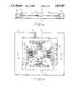
- FIGS. 1A and 1Bare diagrammatic top and cross sectional side views, respectively, of a TAB circuit and carrier frame
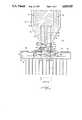
- FIG. 2is a diagrammatic cross sectional front view of the test fixture
- FIG. 3Ais a diagrammatic partial cross sectional side view of a special circuit board that forms a part of the test fixture.
- FIG. 3Bis a diagrammatic top view of the special circuit board.
- Circuit 10includes a circuit die 14 that is surrounded by a body of encapsulation material 16, and is mounted on a Kapton film 18.
- a plurality of conductors 20are etched on the film 18, and provide electrical paths between a plurality of inner lead bond areas 22 of circuit 10 where the conductors are electrically connected to leads (not shown) of die 14, and a plurality of test pads 24 that are disposed around the periphery of circuit 10.
- a plurality of sprocket holes 26are provided in film 18 along two of its edges which are used in the manufacture and handling of circuit 10.
- Carrier frame 12is formed from any suitable material, such as plastic, and is designed in any suitable manner to securely hold the edges of film 18.
- a pair of holes 28are provided in carrier frame 12 to receive test fixture guide rods that help align circuit 10 with the test fixture.
- Fixture 40for receiving circuit 10 and carrier frame 12 in a circuit side down manner.
- Fixture 40includes a layered base structure 41 having a heat sink 42 as its bottom layer, which can be made of any suitable heat conducting material. If desired, heat sink 42 can be cooled by forced air from a fan (not shown). Disposed on top of heat sink 42 near its outer edges, is a layer 44 of thermal insulation. A thermoelectric heat pump 46 is disposed on top of heat sink 42 in an opening in insulation layer 44. The interface between sink 42 and pump 46 can be coated with a thermal grease to reduce the thermal contact resistance.
- thermoelectric heat pump 46is a known type of device which is comprised of an array 47 of two heavily doped semiconductor junctions connected between a pair of smooth ceramic plates.
- a dc voltageWhen a dc voltage is applied to the heat pump, one plate of the pump, depending on the polarity of the voltage, will absorb heat at a rate proportional to the current flowing from the power source. The heat absorbed is transferred to the other plate and must be removed by some means of cooling such as heat sink 42. With these devices, it is possible to obtain differences in temperature of up to 70 degrees Celsius between the two plates. Reversing the direction of the current reverses the heat flow direction.
- These devicescan therefore be used for both heating and cooling an object, and ar thus suitable for use with the present invention, which is designed to subject the circuits under test to temperatures ranging from 20 to 90 degrees Celsius. It will be understood that any suitable type of programmable power supply can be used to control heat pump 46 to automatically vary the device temperature over this range.
- thermoelectric heat pump 46provides an attractive means by which the temperature of a circuit under test can be variably controlled
- the relatively low efficiency of this type of heat pumpindicates that the size of the pump must be considerably larger than the circuit to be able to cool it down to the low end of the specified temperature range.
- a copper thermal chuck or heat spreader 48is disposed on top of heat pump 46 which provides a good thermal path between pump 46 and circuit die 14 when the circuit is in position on the test fixture.
- Chuck 48is a three tiered structure that includes a large bottom pedestal 48a, a middle pedestal 48b, and a small top pedestal 48c. Bottom pedestal 48a is attached directly to the top of heat pump 46, while top pedestal 48c is designed to contact circuit die 14 when carrier 12 is in position.
- a thin sheet of thermally conductive material 50is placed on top pedestal 48c.
- This materialis a thermal conductor when placed under pressure, and consists of a thin metal sheet that is coated on both sides with a silicon rubber.
- Such a materialis manufactured by the Bergquist Company of Minneapolis, Minn. under the name Q-PAD.
- main circuit board 52Disposed on top of insulation layer 44, and bottom pedestal 48a, is a horizontally disposed main circuit board 52, for supplying power and test signals to the circuit under test. To maintain a 50 ohm transmission line to the circuit, conventional microstrip design techniques are employed on the main circuit board 52 by providing an embedded constant voltage reference plane (shown by dashed lines 53).
- test pins 54are soldered to main circuit board 52 and extend vertically through the top of the board as shown. These test pins are electrically connected to the microstrip circuitry in board 52 so that they can transmit power and control signals to the test pads 24 of circuit 10 when it is in position on the test fixture.
- a second special circuit board 56is horizontally disposed on middle pedestal 48b of thermal chuck 48 and on the inner portions of main circuit board 52 over pins 54. This special board serves to maintain a controlled 50 ohm signal path through test pins 54, and all the way to the inner lead bond areas 22 of circuit 10, and is shown in greater detail in FIGS. 3A and 3B.
- FIG. 3Athere is shown a partial cross sectional view of board 56, which includes an insulating substrate 58.
- a conductive layer 60is disposed on all four edges of substrate 58.
- Each of the test pins 54(one shown) passes through a corresponding one of a plurality of holes 62 disposed in substrate 58, as illustrated in FIG. 3B.
- a ground reference planeis established for each of the test pins 54. In this manner, a controlled impedance path is obtained along test pins 54, since each of the pins is disposed parallel to, and at a fixed distance from, this reference plane.
- Conductive layer 60also extends along the top of substrate 58 so that a ground reference plane will also be established for circuit conductors 20 when circuit 10 is disposed in position on top of board 56. Also, a voltage reference plane is established by a second horizontally disposed conductive layer 64 that is embedded within substrate 58. In this manner, a 50 ohm controlled impedance path can also be established along conductors 20 of circuit 10 between test pads 24, and inner lead bond areas 22. To obtain the desired impedance, a thin dielectric polymer layer 66 is disposed over the top portion of first conductive layer 60 to control the spacing between conductors 20 of circuit 10 and the voltage and ground references planes of special circuit board 56, when the circuit 10 is in position on the same.
- the thickness of the dielectric layer 66 in that regionwould have to be correspondingly reduced as well.
- special circuit board 56includes a rectangular opening 68 in the center thereof so that the top pedestal 48c of thermal chuck 48 can make contact with circuit die 14. Also, conductive layer 60 is shown as extending to only a small number of the test pin holes 62 which are labeled 62a. These are the holes which are to receive the ground test pins.
- test pins holes 62bTwo of the test pins holes, labeled 62b, are also electrically isolated from conductive layer 60, and are connected below to the second conductive layer 64. These holes receive the power supply test pins, and provide for capacitive decoupling of the power supply connections to the circuit under test.
- Sheet capacitanceis provided both in the special circuit board 56 and the main circuit board 52 in this manner by placing both power signals in circuit board layers that are in close physical proximity to one another.
- a pair of guide rods 70extend vertically from thermal chuck 48 through main circuit board 52. These guide rods are positioned to pass through the holes 28 in carrier frame 12 to guide the carrier into position on the test fixture 40. When carrier frame 12 is in position, the face down circuit die 14 will rest on top of thermal chuck 48, and, test pads 24 will contact the tops of test pins 54.
- Anvil 72is utilized to apply pressure to these areas of the circuit 10.
- Anvil 72includes an outer weight 74, and a center weight 76, both of which are independent of one another so that the pressure applied to the test pads 24 is independent of the pressure applied to circuit die 14.
- outer weight 74Disposed in the bottom portion of outer weight 74, are two holes 78 for reception of guide rods 70.
- a pair of cavities 80are disposed in the upper portion of outer weight 74 that can be filled with lead beads, or other material, to adjust the weight of the outer weight as necessary to obtain the desired level of pressure on test pads 24. Similar cavities can also be disposed in center weight 76 if desired for adjustment of its weight as well.
- a pair of silicon rubber strips 82are disposed on the bottom of outer weight 74, which are positioned to contact Kapton film 18 of circuit 10 directly opposite test pads 24. These rubber strips transmit the weight of outer weight 74 to the test pad/test pin connections, and accommodate any dimensional mismatches in the test pins 54.
- Anvil center weight 76includes a narrow elongated bottom portion 84 which passes through a centrally disposed opening 86 in outer weight 74. Disposed on the end of bottom portion 84 is another silicon rubber strip 88, which is generally the same size and shape as that of circuit die 14, and is positioned to contact the encapsulation material directly opposite the die. Again, this strip accommodates dimensional mismatches between die 14 and center weight 76, and transmits pressure froom the weight to the die 14 to insure good thermal contact between the die and the sheet 50, and between sheet 50 and thermal chuck 48.
- test fixture 40provides good electrical connections to the circuit 10 through the use of test pins 54 and anvil 72. Proper signal integrity is obtained by maintaining a 50 ohm transmission line to the circuit die 14 through the use of main and special circuit boards 52 and 56, and their voltage and ground reference planes. Finally, the temperature of the circuit 10 is controllable over a wide range through the use of thermoelectric heat pump 46, thermal chuck 48, and heat sink 42.
Landscapes
- Physics & Mathematics (AREA)
- General Physics & Mathematics (AREA)
- Testing Of Individual Semiconductor Devices (AREA)
- Measuring Leads Or Probes (AREA)
Abstract
Description
Claims (9)
Priority Applications (5)
| Application Number | Priority Date | Filing Date | Title |
|---|---|---|---|
| US07/174,697US4839587A (en) | 1988-03-29 | 1988-03-29 | Test fixture for tab circuits and devices |
| CA000594756ACA1293336C (en) | 1988-03-29 | 1989-03-23 | Test fixture for tab circuits and devices |
| EP89904909AEP0400094A1 (en) | 1988-03-29 | 1989-03-28 | Test fixture for tab circuits and devices |
| JP1504707AJPH02500222A (en) | 1988-03-29 | 1989-03-28 | Test equipment for TAB circuits and devices |
| PCT/US1989/001206WO1989009410A1 (en) | 1988-03-29 | 1989-03-28 | Test fixture for tab circuits and devices |
Applications Claiming Priority (1)
| Application Number | Priority Date | Filing Date | Title |
|---|---|---|---|
| US07/174,697US4839587A (en) | 1988-03-29 | 1988-03-29 | Test fixture for tab circuits and devices |
Publications (1)
| Publication Number | Publication Date |
|---|---|
| US4839587Atrue US4839587A (en) | 1989-06-13 |
Family
ID=22637153
Family Applications (1)
| Application Number | Title | Priority Date | Filing Date |
|---|---|---|---|
| US07/174,697Expired - LifetimeUS4839587A (en) | 1988-03-29 | 1988-03-29 | Test fixture for tab circuits and devices |
Country Status (5)
| Country | Link |
|---|---|
| US (1) | US4839587A (en) |
| EP (1) | EP0400094A1 (en) |
| JP (1) | JPH02500222A (en) |
| CA (1) | CA1293336C (en) |
| WO (1) | WO1989009410A1 (en) |
Cited By (115)
| Publication number | Priority date | Publication date | Assignee | Title |
|---|---|---|---|---|
| US4978914A (en)* | 1988-03-15 | 1990-12-18 | Furukawa Denki Kogyo Kabushiki Kaisha | Laminated board for testing electronic components |
| US5006796A (en)* | 1987-10-28 | 1991-04-09 | Irish Transformers Limited | Temperature control instrument for electronic components under test |
| US5036380A (en)* | 1988-03-28 | 1991-07-30 | Digital Equipment Corp. | Burn-in pads for tab interconnects |
| US5122736A (en)* | 1990-12-17 | 1992-06-16 | Intelmatec Corporation | Apparatus for and method of pressing pins of an IC for testing |
| US5124639A (en)* | 1990-11-20 | 1992-06-23 | Motorola, Inc. | Probe card apparatus having a heating element and process for using the same |
| US5124644A (en)* | 1990-12-19 | 1992-06-23 | Vlsi Technology, Inc. | System for positioning a semiconductor chip package with respect to a testing device |
| US5189363A (en)* | 1990-09-14 | 1993-02-23 | Ibm Corporation | Integrated circuit testing system having a cantilevered contact lead probe pattern mounted on a flexible tape for interconnecting an integrated circuit to a tester |
| WO1993004375A1 (en)* | 1991-08-23 | 1993-03-04 | Nchip, Inc. | Burn-in technologies for unpackaged integrated circuits |
| US5196785A (en)* | 1990-12-12 | 1993-03-23 | Hewlett-Packard Company | Tape automated bonding test apparatus for thermal, mechanical and electrical coupling |
| US5227717A (en)* | 1991-12-03 | 1993-07-13 | Sym-Tek Systems, Inc. | Contact assembly for automatic test handler |
| EP0503835A3 (en)* | 1991-03-08 | 1994-03-30 | Hewlett Packard Co | |
| US5331273A (en)* | 1992-04-10 | 1994-07-19 | The United States Of America As Represented By The Secretary Of The Navy | Thermal fixture for testing an integrated circuit |
| US5347215A (en)* | 1991-06-27 | 1994-09-13 | Digital Equipment International Ltd. | Semiconductor chip test jig |
| US5440231A (en)* | 1993-04-19 | 1995-08-08 | Motorola, Inc. | Method and apparatus for coupling a semiconductor device with a tester |
| US5451866A (en)* | 1994-08-26 | 1995-09-19 | The United States Of America As Represented By The Secretary Of The Army | Quick-mount measuring device for evaluating the electrical characteristics of ferroelectric materials |
| US5541524A (en)* | 1991-08-23 | 1996-07-30 | Nchip, Inc. | Burn-in technologies for unpackaged integrated circuits |
| US5757200A (en)* | 1995-03-16 | 1998-05-26 | Advantest Corp. | Lead press mechanism for IC test handler |
| US6049217A (en)* | 1997-12-30 | 2000-04-11 | Intel Corporation | Thermally enhanced test contactor |
| US6072322A (en)* | 1997-12-30 | 2000-06-06 | Intel Corporation | Thermally enhanced test socket |
| US6078185A (en)* | 1996-07-29 | 2000-06-20 | Ando Electric Co., Ltd | Apparatus for controlling insertion of an integrated circuit into a socket for testing and measurement |
| US6215323B1 (en) | 1999-05-28 | 2001-04-10 | Melexis N.V. | Method and apparatus for temperature-controlled testing of integrated circuits |
| US6279832B1 (en) | 1999-03-31 | 2001-08-28 | Melexis Nv | Temperature control system |
| US6323665B1 (en)* | 1997-10-07 | 2001-11-27 | Reliability Incorporated | Apparatus capable of high power dissipation during burn-in of a device under test |
| US6392431B1 (en)* | 1996-10-23 | 2002-05-21 | Aetrium, Inc. | Flexibly suspended heat exchange head for a DUT |
| US6583637B2 (en)* | 2000-06-16 | 2003-06-24 | Murata Manufacturing Co., Ltd. | Load-control-type actuator |
| US6628132B2 (en)* | 2001-08-10 | 2003-09-30 | Teradyne, Inc. | Methods and apparatus for testing a semiconductor structure using improved temperature desoak techniques |
| US6636062B2 (en)* | 2001-04-10 | 2003-10-21 | Delta Design, Inc. | Temperature control device for an electronic component |
| US6744269B1 (en)* | 1997-10-07 | 2004-06-01 | Reliability Incorporated | Burn-in board with adaptable heat sink device |
| US20040263193A1 (en)* | 2003-06-26 | 2004-12-30 | Samsung Electronics Co., Ltd. | Inspecting apparatus for semiconductor device |
| US20050194983A1 (en)* | 1992-06-11 | 2005-09-08 | Schwindt Randy J. | Wafer probe station having a skirting component |
| US6982566B1 (en)* | 2004-04-01 | 2006-01-03 | Altera Corporation | Method and apparatus for operating a burn-in board to achieve lower equilibrium temperature and to minimize thermal runaway |
| US6995582B2 (en)* | 2000-01-13 | 2006-02-07 | Infineon Technologies Ag | Testing device with a contact for connecting to a contact of a semiconductor component |
| US20060158854A1 (en)* | 2005-01-14 | 2006-07-20 | Delta Design, Inc. | Heat sink pedestal with interface medium chamber |
| US7138813B2 (en) | 1999-06-30 | 2006-11-21 | Cascade Microtech, Inc. | Probe station thermal chuck with shielding for capacitive current |
| US7138810B2 (en) | 2002-11-08 | 2006-11-21 | Cascade Microtech, Inc. | Probe station with low noise characteristics |
| US7164279B2 (en) | 1995-04-14 | 2007-01-16 | Cascade Microtech, Inc. | System for evaluating probing networks |
| US7176705B2 (en) | 2004-06-07 | 2007-02-13 | Cascade Microtech, Inc. | Thermal optical chuck |
| US7187188B2 (en) | 2003-12-24 | 2007-03-06 | Cascade Microtech, Inc. | Chuck with integrated wafer support |
| US7190181B2 (en) | 1997-06-06 | 2007-03-13 | Cascade Microtech, Inc. | Probe station having multiple enclosures |
| US7221146B2 (en) | 2002-12-13 | 2007-05-22 | Cascade Microtech, Inc. | Guarded tub enclosure |
| US7221172B2 (en) | 2003-05-06 | 2007-05-22 | Cascade Microtech, Inc. | Switched suspended conductor and connection |
| US7250779B2 (en) | 2002-11-25 | 2007-07-31 | Cascade Microtech, Inc. | Probe station with low inductance path |
| US7250626B2 (en) | 2003-10-22 | 2007-07-31 | Cascade Microtech, Inc. | Probe testing structure |
| US7268533B2 (en) | 2001-08-31 | 2007-09-11 | Cascade Microtech, Inc. | Optical testing device |
| US7304488B2 (en) | 2002-05-23 | 2007-12-04 | Cascade Microtech, Inc. | Shielded probe for high-frequency testing of a device under test |
| US7330041B2 (en) | 2004-06-14 | 2008-02-12 | Cascade Microtech, Inc. | Localizing a temperature of a device for testing |
| US7348787B2 (en) | 1992-06-11 | 2008-03-25 | Cascade Microtech, Inc. | Wafer probe station having environment control enclosure |
| US7352168B2 (en) | 2000-09-05 | 2008-04-01 | Cascade Microtech, Inc. | Chuck for holding a device under test |
| US7355420B2 (en) | 2001-08-21 | 2008-04-08 | Cascade Microtech, Inc. | Membrane probing system |
| US7368925B2 (en) | 2002-01-25 | 2008-05-06 | Cascade Microtech, Inc. | Probe station with two platens |
| US7368927B2 (en) | 2004-07-07 | 2008-05-06 | Cascade Microtech, Inc. | Probe head having a membrane suspended probe |
| US7372285B1 (en)* | 2005-05-25 | 2008-05-13 | National Semiconductor Corporation | Socket-less test board and clamp for electrical testing of integrated circuits |
| US20080116925A1 (en)* | 2006-11-21 | 2008-05-22 | Shinko Electric Industries Co., Ltd. | Probe device |
| US7403028B2 (en) | 2006-06-12 | 2008-07-22 | Cascade Microtech, Inc. | Test structure and probe for differential signals |
| US7403025B2 (en) | 2000-02-25 | 2008-07-22 | Cascade Microtech, Inc. | Membrane probing system |
| US20080174333A1 (en)* | 2007-01-22 | 2008-07-24 | Jun-Pyo Hong | Test sockets having peltier elements, test equipment including the same and methods of testing semiconductor packages using the same |
| US7417446B2 (en) | 2002-11-13 | 2008-08-26 | Cascade Microtech, Inc. | Probe for combined signals |
| US7420381B2 (en) | 2004-09-13 | 2008-09-02 | Cascade Microtech, Inc. | Double sided probing structures |
| US7443186B2 (en) | 2006-06-12 | 2008-10-28 | Cascade Microtech, Inc. | On-wafer test structures for differential signals |
| US7449899B2 (en) | 2005-06-08 | 2008-11-11 | Cascade Microtech, Inc. | Probe for high frequency signals |
| US7456646B2 (en) | 2000-12-04 | 2008-11-25 | Cascade Microtech, Inc. | Wafer probe |
| US7492172B2 (en) | 2003-05-23 | 2009-02-17 | Cascade Microtech, Inc. | Chuck for holding a device under test |
| US7498829B2 (en) | 2003-05-23 | 2009-03-03 | Cascade Microtech, Inc. | Shielded probe for testing a device under test |
| US7504842B2 (en) | 1997-05-28 | 2009-03-17 | Cascade Microtech, Inc. | Probe holder for testing of a test device |
| US7533462B2 (en) | 1999-06-04 | 2009-05-19 | Cascade Microtech, Inc. | Method of constructing a membrane probe |
| US7535247B2 (en) | 2005-01-31 | 2009-05-19 | Cascade Microtech, Inc. | Interface for testing semiconductors |
| US7541821B2 (en) | 1996-08-08 | 2009-06-02 | Cascade Microtech, Inc. | Membrane probing system with local contact scrub |
| US7554322B2 (en) | 2000-09-05 | 2009-06-30 | Cascade Microtech, Inc. | Probe station |
| US7609077B2 (en) | 2006-06-09 | 2009-10-27 | Cascade Microtech, Inc. | Differential signal probe with integral balun |
| US7619419B2 (en) | 2005-06-13 | 2009-11-17 | Cascade Microtech, Inc. | Wideband active-passive differential signal probe |
| US7656172B2 (en) | 2005-01-31 | 2010-02-02 | Cascade Microtech, Inc. | System for testing semiconductors |
| US7681312B2 (en) | 1998-07-14 | 2010-03-23 | Cascade Microtech, Inc. | Membrane probing system |
| US7723999B2 (en) | 2006-06-12 | 2010-05-25 | Cascade Microtech, Inc. | Calibration structures for differential signal probing |
| US7759953B2 (en) | 2003-12-24 | 2010-07-20 | Cascade Microtech, Inc. | Active wafer probe |
| US7764072B2 (en) | 2006-06-12 | 2010-07-27 | Cascade Microtech, Inc. | Differential signal probing system |
| US7876114B2 (en) | 2007-08-08 | 2011-01-25 | Cascade Microtech, Inc. | Differential waveguide probe |
| US20110035540A1 (en)* | 2009-08-10 | 2011-02-10 | Adtron, Inc. | Flash blade system architecture and method |
| US7888957B2 (en) | 2008-10-06 | 2011-02-15 | Cascade Microtech, Inc. | Probing apparatus with impedance optimized interface |
| US8319503B2 (en) | 2008-11-24 | 2012-11-27 | Cascade Microtech, Inc. | Test apparatus for measuring a characteristic of a device under test |
| US8410806B2 (en) | 2008-11-21 | 2013-04-02 | Cascade Microtech, Inc. | Replaceable coupon for a probing apparatus |
| WO2014138428A3 (en)* | 2013-03-08 | 2015-01-08 | SMART Storage Systems, Inc. | Test system with localized heating and method of manufacture thereof |
| US8935466B2 (en) | 2011-03-28 | 2015-01-13 | SMART Storage Systems, Inc. | Data storage system with non-volatile memory and method of operation thereof |
| US8949689B2 (en) | 2012-06-11 | 2015-02-03 | SMART Storage Systems, Inc. | Storage control system with data management mechanism and method of operation thereof |
| US9021319B2 (en) | 2011-09-02 | 2015-04-28 | SMART Storage Systems, Inc. | Non-volatile memory management system with load leveling and method of operation thereof |
| US9043780B2 (en) | 2013-03-27 | 2015-05-26 | SMART Storage Systems, Inc. | Electronic system with system modification control mechanism and method of operation thereof |
| US9063844B2 (en) | 2011-09-02 | 2015-06-23 | SMART Storage Systems, Inc. | Non-volatile memory management system with time measure mechanism and method of operation thereof |
| US9098399B2 (en) | 2011-08-31 | 2015-08-04 | SMART Storage Systems, Inc. | Electronic system with storage management mechanism and method of operation thereof |
| US9123445B2 (en) | 2013-01-22 | 2015-09-01 | SMART Storage Systems, Inc. | Storage control system with data management mechanism and method of operation thereof |
| US9146850B2 (en) | 2013-08-01 | 2015-09-29 | SMART Storage Systems, Inc. | Data storage system with dynamic read threshold mechanism and method of operation thereof |
| US9152555B2 (en) | 2013-11-15 | 2015-10-06 | Sandisk Enterprise IP LLC. | Data management with modular erase in a data storage system |
| US9158349B2 (en) | 2013-10-04 | 2015-10-13 | Sandisk Enterprise Ip Llc | System and method for heat dissipation |
| US9170941B2 (en) | 2013-04-05 | 2015-10-27 | Sandisk Enterprises IP LLC | Data hardening in a storage system |
| US9183137B2 (en) | 2013-02-27 | 2015-11-10 | SMART Storage Systems, Inc. | Storage control system with data management mechanism and method of operation thereof |
| US9214965B2 (en) | 2013-02-20 | 2015-12-15 | Sandisk Enterprise Ip Llc | Method and system for improving data integrity in non-volatile storage |
| US9239781B2 (en) | 2012-02-07 | 2016-01-19 | SMART Storage Systems, Inc. | Storage control system with erase block mechanism and method of operation thereof |
| US9244519B1 (en) | 2013-06-25 | 2016-01-26 | Smart Storage Systems. Inc. | Storage system with data transfer rate adjustment for power throttling |
| US9313874B2 (en) | 2013-06-19 | 2016-04-12 | SMART Storage Systems, Inc. | Electronic system with heat extraction and method of manufacture thereof |
| US9329928B2 (en) | 2013-02-20 | 2016-05-03 | Sandisk Enterprise IP LLC. | Bandwidth optimization in a non-volatile memory system |
| US9348377B2 (en) | 2014-03-14 | 2016-05-24 | Sandisk Enterprise Ip Llc | Thermal isolation techniques |
| US9361222B2 (en) | 2013-08-07 | 2016-06-07 | SMART Storage Systems, Inc. | Electronic system with storage drive life estimation mechanism and method of operation thereof |
| US9367353B1 (en) | 2013-06-25 | 2016-06-14 | Sandisk Technologies Inc. | Storage control system with power throttling mechanism and method of operation thereof |
| US9431113B2 (en) | 2013-08-07 | 2016-08-30 | Sandisk Technologies Llc | Data storage system with dynamic erase block grouping mechanism and method of operation thereof |
| US9485851B2 (en) | 2014-03-14 | 2016-11-01 | Sandisk Technologies Llc | Thermal tube assembly structures |
| US9497889B2 (en) | 2014-02-27 | 2016-11-15 | Sandisk Technologies Llc | Heat dissipation for substrate assemblies |
| US9519319B2 (en) | 2014-03-14 | 2016-12-13 | Sandisk Technologies Llc | Self-supporting thermal tube structure for electronic assemblies |
| US9543025B2 (en) | 2013-04-11 | 2017-01-10 | Sandisk Technologies Llc | Storage control system with power-off time estimation mechanism and method of operation thereof |
| US9549457B2 (en) | 2014-02-12 | 2017-01-17 | Sandisk Technologies Llc | System and method for redirecting airflow across an electronic assembly |
| US9671962B2 (en) | 2012-11-30 | 2017-06-06 | Sandisk Technologies Llc | Storage control system with data management mechanism of parity and method of operation thereof |
| US9898056B2 (en) | 2013-06-19 | 2018-02-20 | Sandisk Technologies Llc | Electronic assembly with thermal channel and method of manufacture thereof |
| US10013033B2 (en) | 2013-06-19 | 2018-07-03 | Sandisk Technologies Llc | Electronic assembly with thermal channel and method of manufacture thereof |
| US10049037B2 (en) | 2013-04-05 | 2018-08-14 | Sandisk Enterprise Ip Llc | Data management in a storage system |
| US10546648B2 (en) | 2013-04-12 | 2020-01-28 | Sandisk Technologies Llc | Storage control system with data management mechanism and method of operation thereof |
| TWI709521B (en)* | 2019-12-12 | 2020-11-11 | 鴻勁精密股份有限公司 | Attaching mechanism of conveying device and testing equipment for its application |
| TWI709520B (en)* | 2019-12-12 | 2020-11-11 | 鴻勁精密股份有限公司 | Attaching mechanism of conveying device and testing equipment for its application |
| TWI874043B (en)* | 2023-12-14 | 2025-02-21 | 長裕欣業股份有限公司 | Electronic component temperature test apparatus |
Families Citing this family (1)
| Publication number | Priority date | Publication date | Assignee | Title |
|---|---|---|---|---|
| US4512821A (en)* | 1982-12-20 | 1985-04-23 | Procedyne Corp. | Method for metal treatment using a fluidized bed |
Citations (9)
| Publication number | Priority date | Publication date | Assignee | Title |
|---|---|---|---|---|
| US3643201A (en)* | 1970-02-09 | 1972-02-15 | Amp Inc | Impedance matching microstrip connector |
| US3710251A (en)* | 1971-04-07 | 1973-01-09 | Collins Radio Co | Microelectric heat exchanger pedestal |
| US3979671A (en)* | 1975-03-06 | 1976-09-07 | International Business Machines Corporation | Test fixture for use in a high speed electronic semiconductor chip test system |
| US4402185A (en)* | 1982-01-07 | 1983-09-06 | Ncr Corporation | Thermoelectric (peltier effect) hot/cold socket for packaged I.C. microprobing |
| US4560962A (en)* | 1983-08-30 | 1985-12-24 | Burroughs Corporation | Multilayered printed circuit board with controlled 100 ohm impedance |
| US4604572A (en)* | 1981-07-08 | 1986-08-05 | Fujitsu Limited | Device for testing semiconductor devices at a high temperature |
| US4616178A (en)* | 1982-05-27 | 1986-10-07 | Harris Corporation | Pulsed linear integrated circuit tester |
| US4672313A (en)* | 1983-02-24 | 1987-06-09 | Commissariat A L'energie Atomique | Device for checking mobile electrical charges in a MOS integrated circuit |
| US4727720A (en)* | 1986-04-21 | 1988-03-01 | Wernicki Paul F | Combination ice mold and ice extractor |
Family Cites Families (1)
| Publication number | Priority date | Publication date | Assignee | Title |
|---|---|---|---|---|
| US4686468A (en)* | 1984-12-10 | 1987-08-11 | Aseco Corporation | Contact set for test apparatus for testing integrated circuit package |
- 1988
- 1988-03-29USUS07/174,697patent/US4839587A/ennot_activeExpired - Lifetime
- 1989
- 1989-03-23CACA000594756Apatent/CA1293336C/ennot_activeExpired - Fee Related
- 1989-03-28WOPCT/US1989/001206patent/WO1989009410A1/ennot_activeApplication Discontinuation
- 1989-03-28EPEP89904909Apatent/EP0400094A1/ennot_activeWithdrawn
- 1989-03-28JPJP1504707Apatent/JPH02500222A/enactivePending
Patent Citations (9)
| Publication number | Priority date | Publication date | Assignee | Title |
|---|---|---|---|---|
| US3643201A (en)* | 1970-02-09 | 1972-02-15 | Amp Inc | Impedance matching microstrip connector |
| US3710251A (en)* | 1971-04-07 | 1973-01-09 | Collins Radio Co | Microelectric heat exchanger pedestal |
| US3979671A (en)* | 1975-03-06 | 1976-09-07 | International Business Machines Corporation | Test fixture for use in a high speed electronic semiconductor chip test system |
| US4604572A (en)* | 1981-07-08 | 1986-08-05 | Fujitsu Limited | Device for testing semiconductor devices at a high temperature |
| US4402185A (en)* | 1982-01-07 | 1983-09-06 | Ncr Corporation | Thermoelectric (peltier effect) hot/cold socket for packaged I.C. microprobing |
| US4616178A (en)* | 1982-05-27 | 1986-10-07 | Harris Corporation | Pulsed linear integrated circuit tester |
| US4672313A (en)* | 1983-02-24 | 1987-06-09 | Commissariat A L'energie Atomique | Device for checking mobile electrical charges in a MOS integrated circuit |
| US4560962A (en)* | 1983-08-30 | 1985-12-24 | Burroughs Corporation | Multilayered printed circuit board with controlled 100 ohm impedance |
| US4727720A (en)* | 1986-04-21 | 1988-03-01 | Wernicki Paul F | Combination ice mold and ice extractor |
Cited By (176)
| Publication number | Priority date | Publication date | Assignee | Title |
|---|---|---|---|---|
| US5006796A (en)* | 1987-10-28 | 1991-04-09 | Irish Transformers Limited | Temperature control instrument for electronic components under test |
| US4978914A (en)* | 1988-03-15 | 1990-12-18 | Furukawa Denki Kogyo Kabushiki Kaisha | Laminated board for testing electronic components |
| US5036380A (en)* | 1988-03-28 | 1991-07-30 | Digital Equipment Corp. | Burn-in pads for tab interconnects |
| US5189363A (en)* | 1990-09-14 | 1993-02-23 | Ibm Corporation | Integrated circuit testing system having a cantilevered contact lead probe pattern mounted on a flexible tape for interconnecting an integrated circuit to a tester |
| US5124639A (en)* | 1990-11-20 | 1992-06-23 | Motorola, Inc. | Probe card apparatus having a heating element and process for using the same |
| US5196785A (en)* | 1990-12-12 | 1993-03-23 | Hewlett-Packard Company | Tape automated bonding test apparatus for thermal, mechanical and electrical coupling |
| US5122736A (en)* | 1990-12-17 | 1992-06-16 | Intelmatec Corporation | Apparatus for and method of pressing pins of an IC for testing |
| WO1992011540A1 (en)* | 1990-12-19 | 1992-07-09 | Vlsi Technology, Inc. | System for positioning a semiconductor chip package with respect to a testing device |
| US5124644A (en)* | 1990-12-19 | 1992-06-23 | Vlsi Technology, Inc. | System for positioning a semiconductor chip package with respect to a testing device |
| EP0503835A3 (en)* | 1991-03-08 | 1994-03-30 | Hewlett Packard Co | |
| US5347215A (en)* | 1991-06-27 | 1994-09-13 | Digital Equipment International Ltd. | Semiconductor chip test jig |
| WO1993004375A1 (en)* | 1991-08-23 | 1993-03-04 | Nchip, Inc. | Burn-in technologies for unpackaged integrated circuits |
| US5541524A (en)* | 1991-08-23 | 1996-07-30 | Nchip, Inc. | Burn-in technologies for unpackaged integrated circuits |
| US5397997A (en)* | 1991-08-23 | 1995-03-14 | Nchip, Inc. | Burn-in technologies for unpackaged integrated circuits |
| US5227717A (en)* | 1991-12-03 | 1993-07-13 | Sym-Tek Systems, Inc. | Contact assembly for automatic test handler |
| US5331273A (en)* | 1992-04-10 | 1994-07-19 | The United States Of America As Represented By The Secretary Of The Navy | Thermal fixture for testing an integrated circuit |
| US7348787B2 (en) | 1992-06-11 | 2008-03-25 | Cascade Microtech, Inc. | Wafer probe station having environment control enclosure |
| US7492147B2 (en) | 1992-06-11 | 2009-02-17 | Cascade Microtech, Inc. | Wafer probe station having a skirting component |
| US7330023B2 (en) | 1992-06-11 | 2008-02-12 | Cascade Microtech, Inc. | Wafer probe station having a skirting component |
| US7595632B2 (en) | 1992-06-11 | 2009-09-29 | Cascade Microtech, Inc. | Wafer probe station having environment control enclosure |
| US20050194983A1 (en)* | 1992-06-11 | 2005-09-08 | Schwindt Randy J. | Wafer probe station having a skirting component |
| US7589518B2 (en) | 1992-06-11 | 2009-09-15 | Cascade Microtech, Inc. | Wafer probe station having a skirting component |
| US5440231A (en)* | 1993-04-19 | 1995-08-08 | Motorola, Inc. | Method and apparatus for coupling a semiconductor device with a tester |
| US5691650A (en)* | 1993-04-19 | 1997-11-25 | Motorola, Inc. | Apparatus for coupling a semiconductor device with a tester |
| US5451866A (en)* | 1994-08-26 | 1995-09-19 | The United States Of America As Represented By The Secretary Of The Army | Quick-mount measuring device for evaluating the electrical characteristics of ferroelectric materials |
| US5757200A (en)* | 1995-03-16 | 1998-05-26 | Advantest Corp. | Lead press mechanism for IC test handler |
| US7321233B2 (en) | 1995-04-14 | 2008-01-22 | Cascade Microtech, Inc. | System for evaluating probing networks |
| US7164279B2 (en) | 1995-04-14 | 2007-01-16 | Cascade Microtech, Inc. | System for evaluating probing networks |
| US6078185A (en)* | 1996-07-29 | 2000-06-20 | Ando Electric Co., Ltd | Apparatus for controlling insertion of an integrated circuit into a socket for testing and measurement |
| US7893704B2 (en) | 1996-08-08 | 2011-02-22 | Cascade Microtech, Inc. | Membrane probing structure with laterally scrubbing contacts |
| US7541821B2 (en) | 1996-08-08 | 2009-06-02 | Cascade Microtech, Inc. | Membrane probing system with local contact scrub |
| US6392431B1 (en)* | 1996-10-23 | 2002-05-21 | Aetrium, Inc. | Flexibly suspended heat exchange head for a DUT |
| US7504842B2 (en) | 1997-05-28 | 2009-03-17 | Cascade Microtech, Inc. | Probe holder for testing of a test device |
| US7436170B2 (en) | 1997-06-06 | 2008-10-14 | Cascade Microtech, Inc. | Probe station having multiple enclosures |
| US7626379B2 (en) | 1997-06-06 | 2009-12-01 | Cascade Microtech, Inc. | Probe station having multiple enclosures |
| US7190181B2 (en) | 1997-06-06 | 2007-03-13 | Cascade Microtech, Inc. | Probe station having multiple enclosures |
| US6323665B1 (en)* | 1997-10-07 | 2001-11-27 | Reliability Incorporated | Apparatus capable of high power dissipation during burn-in of a device under test |
| US6744269B1 (en)* | 1997-10-07 | 2004-06-01 | Reliability Incorporated | Burn-in board with adaptable heat sink device |
| US6049217A (en)* | 1997-12-30 | 2000-04-11 | Intel Corporation | Thermally enhanced test contactor |
| US6072322A (en)* | 1997-12-30 | 2000-06-06 | Intel Corporation | Thermally enhanced test socket |
| US7681312B2 (en) | 1998-07-14 | 2010-03-23 | Cascade Microtech, Inc. | Membrane probing system |
| US7761986B2 (en) | 1998-07-14 | 2010-07-27 | Cascade Microtech, Inc. | Membrane probing method using improved contact |
| US8451017B2 (en) | 1998-07-14 | 2013-05-28 | Cascade Microtech, Inc. | Membrane probing method using improved contact |
| US6467697B2 (en) | 1999-03-31 | 2002-10-22 | Melexis Nv | Temperature control system |
| US6279832B1 (en) | 1999-03-31 | 2001-08-28 | Melexis Nv | Temperature control system |
| US6215323B1 (en) | 1999-05-28 | 2001-04-10 | Melexis N.V. | Method and apparatus for temperature-controlled testing of integrated circuits |
| US7533462B2 (en) | 1999-06-04 | 2009-05-19 | Cascade Microtech, Inc. | Method of constructing a membrane probe |
| US7138813B2 (en) | 1999-06-30 | 2006-11-21 | Cascade Microtech, Inc. | Probe station thermal chuck with shielding for capacitive current |
| US7616017B2 (en) | 1999-06-30 | 2009-11-10 | Cascade Microtech, Inc. | Probe station thermal chuck with shielding for capacitive current |
| US7292057B2 (en) | 1999-06-30 | 2007-11-06 | Cascade Microtech, Inc. | Probe station thermal chuck with shielding for capacitive current |
| US6995582B2 (en)* | 2000-01-13 | 2006-02-07 | Infineon Technologies Ag | Testing device with a contact for connecting to a contact of a semiconductor component |
| US7403025B2 (en) | 2000-02-25 | 2008-07-22 | Cascade Microtech, Inc. | Membrane probing system |
| US6583637B2 (en)* | 2000-06-16 | 2003-06-24 | Murata Manufacturing Co., Ltd. | Load-control-type actuator |
| US7501810B2 (en) | 2000-09-05 | 2009-03-10 | Cascade Microtech, Inc. | Chuck for holding a device under test |
| US7554322B2 (en) | 2000-09-05 | 2009-06-30 | Cascade Microtech, Inc. | Probe station |
| US7423419B2 (en) | 2000-09-05 | 2008-09-09 | Cascade Microtech, Inc. | Chuck for holding a device under test |
| US7969173B2 (en) | 2000-09-05 | 2011-06-28 | Cascade Microtech, Inc. | Chuck for holding a device under test |
| US7518358B2 (en) | 2000-09-05 | 2009-04-14 | Cascade Microtech, Inc. | Chuck for holding a device under test |
| US7352168B2 (en) | 2000-09-05 | 2008-04-01 | Cascade Microtech, Inc. | Chuck for holding a device under test |
| US7514915B2 (en) | 2000-09-05 | 2009-04-07 | Cascade Microtech, Inc. | Chuck for holding a device under test |
| US7688062B2 (en) | 2000-09-05 | 2010-03-30 | Cascade Microtech, Inc. | Probe station |
| US7761983B2 (en) | 2000-12-04 | 2010-07-27 | Cascade Microtech, Inc. | Method of assembling a wafer probe |
| US7495461B2 (en) | 2000-12-04 | 2009-02-24 | Cascade Microtech, Inc. | Wafer probe |
| US7688097B2 (en) | 2000-12-04 | 2010-03-30 | Cascade Microtech, Inc. | Wafer probe |
| US7456646B2 (en) | 2000-12-04 | 2008-11-25 | Cascade Microtech, Inc. | Wafer probe |
| US20040036492A1 (en)* | 2001-04-10 | 2004-02-26 | Gaasch Thomas Francis | Method for controlling the temperature of an electronic component under test |
| US6886976B2 (en) | 2001-04-10 | 2005-05-03 | Delta Design, Inc. | Method for controlling the temperature of an electronic component under test |
| US6636062B2 (en)* | 2001-04-10 | 2003-10-21 | Delta Design, Inc. | Temperature control device for an electronic component |
| US6628132B2 (en)* | 2001-08-10 | 2003-09-30 | Teradyne, Inc. | Methods and apparatus for testing a semiconductor structure using improved temperature desoak techniques |
| US7492175B2 (en) | 2001-08-21 | 2009-02-17 | Cascade Microtech, Inc. | Membrane probing system |
| US7355420B2 (en) | 2001-08-21 | 2008-04-08 | Cascade Microtech, Inc. | Membrane probing system |
| US7268533B2 (en) | 2001-08-31 | 2007-09-11 | Cascade Microtech, Inc. | Optical testing device |
| US7368925B2 (en) | 2002-01-25 | 2008-05-06 | Cascade Microtech, Inc. | Probe station with two platens |
| US7436194B2 (en) | 2002-05-23 | 2008-10-14 | Cascade Microtech, Inc. | Shielded probe with low contact resistance for testing a device under test |
| US7482823B2 (en) | 2002-05-23 | 2009-01-27 | Cascade Microtech, Inc. | Shielded probe for testing a device under test |
| US7489149B2 (en) | 2002-05-23 | 2009-02-10 | Cascade Microtech, Inc. | Shielded probe for testing a device under test |
| US7518387B2 (en) | 2002-05-23 | 2009-04-14 | Cascade Microtech, Inc. | Shielded probe for testing a device under test |
| US7304488B2 (en) | 2002-05-23 | 2007-12-04 | Cascade Microtech, Inc. | Shielded probe for high-frequency testing of a device under test |
| US7138810B2 (en) | 2002-11-08 | 2006-11-21 | Cascade Microtech, Inc. | Probe station with low noise characteristics |
| US7295025B2 (en) | 2002-11-08 | 2007-11-13 | Cascade Microtech, Inc. | Probe station with low noise characteristics |
| US7550984B2 (en) | 2002-11-08 | 2009-06-23 | Cascade Microtech, Inc. | Probe station with low noise characteristics |
| US7453276B2 (en) | 2002-11-13 | 2008-11-18 | Cascade Microtech, Inc. | Probe for combined signals |
| US7417446B2 (en) | 2002-11-13 | 2008-08-26 | Cascade Microtech, Inc. | Probe for combined signals |
| US7250779B2 (en) | 2002-11-25 | 2007-07-31 | Cascade Microtech, Inc. | Probe station with low inductance path |
| US7498828B2 (en) | 2002-11-25 | 2009-03-03 | Cascade Microtech, Inc. | Probe station with low inductance path |
| US7639003B2 (en) | 2002-12-13 | 2009-12-29 | Cascade Microtech, Inc. | Guarded tub enclosure |
| US7221146B2 (en) | 2002-12-13 | 2007-05-22 | Cascade Microtech, Inc. | Guarded tub enclosure |
| US7468609B2 (en) | 2003-05-06 | 2008-12-23 | Cascade Microtech, Inc. | Switched suspended conductor and connection |
| US7221172B2 (en) | 2003-05-06 | 2007-05-22 | Cascade Microtech, Inc. | Switched suspended conductor and connection |
| US7492172B2 (en) | 2003-05-23 | 2009-02-17 | Cascade Microtech, Inc. | Chuck for holding a device under test |
| US7501842B2 (en) | 2003-05-23 | 2009-03-10 | Cascade Microtech, Inc. | Shielded probe for testing a device under test |
| US7498829B2 (en) | 2003-05-23 | 2009-03-03 | Cascade Microtech, Inc. | Shielded probe for testing a device under test |
| US7898273B2 (en) | 2003-05-23 | 2011-03-01 | Cascade Microtech, Inc. | Probe for testing a device under test |
| US7876115B2 (en) | 2003-05-23 | 2011-01-25 | Cascade Microtech, Inc. | Chuck for holding a device under test |
| US7034557B2 (en)* | 2003-06-26 | 2006-04-25 | Samsung Electronics Co., Ltd. | Inspecting apparatus having a radiator to radiate heat from a semiconductor device |
| US20040263193A1 (en)* | 2003-06-26 | 2004-12-30 | Samsung Electronics Co., Ltd. | Inspecting apparatus for semiconductor device |
| US7250626B2 (en) | 2003-10-22 | 2007-07-31 | Cascade Microtech, Inc. | Probe testing structure |
| US8069491B2 (en) | 2003-10-22 | 2011-11-29 | Cascade Microtech, Inc. | Probe testing structure |
| US7187188B2 (en) | 2003-12-24 | 2007-03-06 | Cascade Microtech, Inc. | Chuck with integrated wafer support |
| US7362115B2 (en) | 2003-12-24 | 2008-04-22 | Cascade Microtech, Inc. | Chuck with integrated wafer support |
| US7759953B2 (en) | 2003-12-24 | 2010-07-20 | Cascade Microtech, Inc. | Active wafer probe |
| US7688091B2 (en) | 2003-12-24 | 2010-03-30 | Cascade Microtech, Inc. | Chuck with integrated wafer support |
| US6982566B1 (en)* | 2004-04-01 | 2006-01-03 | Altera Corporation | Method and apparatus for operating a burn-in board to achieve lower equilibrium temperature and to minimize thermal runaway |
| US7504823B2 (en) | 2004-06-07 | 2009-03-17 | Cascade Microtech, Inc. | Thermal optical chuck |
| US7176705B2 (en) | 2004-06-07 | 2007-02-13 | Cascade Microtech, Inc. | Thermal optical chuck |
| US7330041B2 (en) | 2004-06-14 | 2008-02-12 | Cascade Microtech, Inc. | Localizing a temperature of a device for testing |
| US7514944B2 (en) | 2004-07-07 | 2009-04-07 | Cascade Microtech, Inc. | Probe head having a membrane suspended probe |
| US7368927B2 (en) | 2004-07-07 | 2008-05-06 | Cascade Microtech, Inc. | Probe head having a membrane suspended probe |
| US7420381B2 (en) | 2004-09-13 | 2008-09-02 | Cascade Microtech, Inc. | Double sided probing structures |
| US8013623B2 (en) | 2004-09-13 | 2011-09-06 | Cascade Microtech, Inc. | Double sided probing structures |
| US20060158854A1 (en)* | 2005-01-14 | 2006-07-20 | Delta Design, Inc. | Heat sink pedestal with interface medium chamber |
| US20100101088A1 (en)* | 2005-01-14 | 2010-04-29 | Delta Design, Inc. | Method of manufacturing a heat sink pedestal device with interface medium chamber |
| US7986155B2 (en) | 2005-01-14 | 2011-07-26 | Delta Design, Inc. | Method of manufacturing a heat sink pedestal device with interface medium chamber |
| US7639029B2 (en)* | 2005-01-14 | 2009-12-29 | Delta Design, Inc. | Heat sink pedestal with interface medium chamber |
| US7656172B2 (en) | 2005-01-31 | 2010-02-02 | Cascade Microtech, Inc. | System for testing semiconductors |
| US7535247B2 (en) | 2005-01-31 | 2009-05-19 | Cascade Microtech, Inc. | Interface for testing semiconductors |
| US7940069B2 (en) | 2005-01-31 | 2011-05-10 | Cascade Microtech, Inc. | System for testing semiconductors |
| US7898281B2 (en) | 2005-01-31 | 2011-03-01 | Cascade Mircotech, Inc. | Interface for testing semiconductors |
| US7372285B1 (en)* | 2005-05-25 | 2008-05-13 | National Semiconductor Corporation | Socket-less test board and clamp for electrical testing of integrated circuits |
| US7449899B2 (en) | 2005-06-08 | 2008-11-11 | Cascade Microtech, Inc. | Probe for high frequency signals |
| US7619419B2 (en) | 2005-06-13 | 2009-11-17 | Cascade Microtech, Inc. | Wideband active-passive differential signal probe |
| US7609077B2 (en) | 2006-06-09 | 2009-10-27 | Cascade Microtech, Inc. | Differential signal probe with integral balun |
| US7723999B2 (en) | 2006-06-12 | 2010-05-25 | Cascade Microtech, Inc. | Calibration structures for differential signal probing |
| US7403028B2 (en) | 2006-06-12 | 2008-07-22 | Cascade Microtech, Inc. | Test structure and probe for differential signals |
| US7750652B2 (en) | 2006-06-12 | 2010-07-06 | Cascade Microtech, Inc. | Test structure and probe for differential signals |
| US7443186B2 (en) | 2006-06-12 | 2008-10-28 | Cascade Microtech, Inc. | On-wafer test structures for differential signals |
| US7764072B2 (en) | 2006-06-12 | 2010-07-27 | Cascade Microtech, Inc. | Differential signal probing system |
| US20080116925A1 (en)* | 2006-11-21 | 2008-05-22 | Shinko Electric Industries Co., Ltd. | Probe device |
| US7667474B2 (en)* | 2006-11-21 | 2010-02-23 | Shinko Electric Industries Co., Ltd. | Probe device |
| US7659738B2 (en)* | 2007-01-22 | 2010-02-09 | Samsung Electronics Co., Ltd. | Test sockets having peltier elements, test equipment including the same and methods of testing semiconductor packages using the same |
| US20080174333A1 (en)* | 2007-01-22 | 2008-07-24 | Jun-Pyo Hong | Test sockets having peltier elements, test equipment including the same and methods of testing semiconductor packages using the same |
| US7876114B2 (en) | 2007-08-08 | 2011-01-25 | Cascade Microtech, Inc. | Differential waveguide probe |
| US7888957B2 (en) | 2008-10-06 | 2011-02-15 | Cascade Microtech, Inc. | Probing apparatus with impedance optimized interface |
| US9429638B2 (en) | 2008-11-21 | 2016-08-30 | Cascade Microtech, Inc. | Method of replacing an existing contact of a wafer probing assembly |
| US8410806B2 (en) | 2008-11-21 | 2013-04-02 | Cascade Microtech, Inc. | Replaceable coupon for a probing apparatus |
| US10267848B2 (en) | 2008-11-21 | 2019-04-23 | Formfactor Beaverton, Inc. | Method of electrically contacting a bond pad of a device under test with a probe |
| US8319503B2 (en) | 2008-11-24 | 2012-11-27 | Cascade Microtech, Inc. | Test apparatus for measuring a characteristic of a device under test |
| US20110035540A1 (en)* | 2009-08-10 | 2011-02-10 | Adtron, Inc. | Flash blade system architecture and method |
| US8935466B2 (en) | 2011-03-28 | 2015-01-13 | SMART Storage Systems, Inc. | Data storage system with non-volatile memory and method of operation thereof |
| US9098399B2 (en) | 2011-08-31 | 2015-08-04 | SMART Storage Systems, Inc. | Electronic system with storage management mechanism and method of operation thereof |
| US9021319B2 (en) | 2011-09-02 | 2015-04-28 | SMART Storage Systems, Inc. | Non-volatile memory management system with load leveling and method of operation thereof |
| US9063844B2 (en) | 2011-09-02 | 2015-06-23 | SMART Storage Systems, Inc. | Non-volatile memory management system with time measure mechanism and method of operation thereof |
| US9239781B2 (en) | 2012-02-07 | 2016-01-19 | SMART Storage Systems, Inc. | Storage control system with erase block mechanism and method of operation thereof |
| US8949689B2 (en) | 2012-06-11 | 2015-02-03 | SMART Storage Systems, Inc. | Storage control system with data management mechanism and method of operation thereof |
| US9671962B2 (en) | 2012-11-30 | 2017-06-06 | Sandisk Technologies Llc | Storage control system with data management mechanism of parity and method of operation thereof |
| US9123445B2 (en) | 2013-01-22 | 2015-09-01 | SMART Storage Systems, Inc. | Storage control system with data management mechanism and method of operation thereof |
| US9214965B2 (en) | 2013-02-20 | 2015-12-15 | Sandisk Enterprise Ip Llc | Method and system for improving data integrity in non-volatile storage |
| US9329928B2 (en) | 2013-02-20 | 2016-05-03 | Sandisk Enterprise IP LLC. | Bandwidth optimization in a non-volatile memory system |
| US9183137B2 (en) | 2013-02-27 | 2015-11-10 | SMART Storage Systems, Inc. | Storage control system with data management mechanism and method of operation thereof |
| CN105164544A (en)* | 2013-03-08 | 2015-12-16 | 智能存储系统股份有限公司 | Test system with localized heating and method of manufacture |
| WO2014138428A3 (en)* | 2013-03-08 | 2015-01-08 | SMART Storage Systems, Inc. | Test system with localized heating and method of manufacture thereof |
| US9470720B2 (en) | 2013-03-08 | 2016-10-18 | Sandisk Technologies Llc | Test system with localized heating and method of manufacture thereof |
| US9043780B2 (en) | 2013-03-27 | 2015-05-26 | SMART Storage Systems, Inc. | Electronic system with system modification control mechanism and method of operation thereof |
| US9170941B2 (en) | 2013-04-05 | 2015-10-27 | Sandisk Enterprises IP LLC | Data hardening in a storage system |
| US10049037B2 (en) | 2013-04-05 | 2018-08-14 | Sandisk Enterprise Ip Llc | Data management in a storage system |
| US9543025B2 (en) | 2013-04-11 | 2017-01-10 | Sandisk Technologies Llc | Storage control system with power-off time estimation mechanism and method of operation thereof |
| US10546648B2 (en) | 2013-04-12 | 2020-01-28 | Sandisk Technologies Llc | Storage control system with data management mechanism and method of operation thereof |
| US9898056B2 (en) | 2013-06-19 | 2018-02-20 | Sandisk Technologies Llc | Electronic assembly with thermal channel and method of manufacture thereof |
| US9313874B2 (en) | 2013-06-19 | 2016-04-12 | SMART Storage Systems, Inc. | Electronic system with heat extraction and method of manufacture thereof |
| US10013033B2 (en) | 2013-06-19 | 2018-07-03 | Sandisk Technologies Llc | Electronic assembly with thermal channel and method of manufacture thereof |
| US9244519B1 (en) | 2013-06-25 | 2016-01-26 | Smart Storage Systems. Inc. | Storage system with data transfer rate adjustment for power throttling |
| US9367353B1 (en) | 2013-06-25 | 2016-06-14 | Sandisk Technologies Inc. | Storage control system with power throttling mechanism and method of operation thereof |
| US9146850B2 (en) | 2013-08-01 | 2015-09-29 | SMART Storage Systems, Inc. | Data storage system with dynamic read threshold mechanism and method of operation thereof |
| US9431113B2 (en) | 2013-08-07 | 2016-08-30 | Sandisk Technologies Llc | Data storage system with dynamic erase block grouping mechanism and method of operation thereof |
| US9361222B2 (en) | 2013-08-07 | 2016-06-07 | SMART Storage Systems, Inc. | Electronic system with storage drive life estimation mechanism and method of operation thereof |
| US9158349B2 (en) | 2013-10-04 | 2015-10-13 | Sandisk Enterprise Ip Llc | System and method for heat dissipation |
| US9152555B2 (en) | 2013-11-15 | 2015-10-06 | Sandisk Enterprise IP LLC. | Data management with modular erase in a data storage system |
| US9549457B2 (en) | 2014-02-12 | 2017-01-17 | Sandisk Technologies Llc | System and method for redirecting airflow across an electronic assembly |
| US9848512B2 (en) | 2014-02-27 | 2017-12-19 | Sandisk Technologies Llc | Heat dissipation for substrate assemblies |
| US9497889B2 (en) | 2014-02-27 | 2016-11-15 | Sandisk Technologies Llc | Heat dissipation for substrate assemblies |
| US9485851B2 (en) | 2014-03-14 | 2016-11-01 | Sandisk Technologies Llc | Thermal tube assembly structures |
| US9348377B2 (en) | 2014-03-14 | 2016-05-24 | Sandisk Enterprise Ip Llc | Thermal isolation techniques |
| US9519319B2 (en) | 2014-03-14 | 2016-12-13 | Sandisk Technologies Llc | Self-supporting thermal tube structure for electronic assemblies |
| TWI709521B (en)* | 2019-12-12 | 2020-11-11 | 鴻勁精密股份有限公司 | Attaching mechanism of conveying device and testing equipment for its application |
| TWI709520B (en)* | 2019-12-12 | 2020-11-11 | 鴻勁精密股份有限公司 | Attaching mechanism of conveying device and testing equipment for its application |
| TWI874043B (en)* | 2023-12-14 | 2025-02-21 | 長裕欣業股份有限公司 | Electronic component temperature test apparatus |
Also Published As
| Publication number | Publication date |
|---|---|
| CA1293336C (en) | 1991-12-17 |
| WO1989009410A1 (en) | 1989-10-05 |
| JPH02500222A (en) | 1990-01-25 |
| EP0400094A1 (en) | 1990-12-05 |
Similar Documents
| Publication | Publication Date | Title |
|---|---|---|
| US4839587A (en) | Test fixture for tab circuits and devices | |
| US4763409A (en) | Method of manufacturing semiconductor device | |
| US4744007A (en) | High density LSI package for logic circuits | |
| US7932596B2 (en) | Thermally enhanced electronic flip-chip packaging with external-connector-side die and method | |
| US4103318A (en) | Electronic multichip module | |
| US4737839A (en) | Semiconductor chip mounting system | |
| US6028358A (en) | Package for a semiconductor device and a semiconductor device | |
| US4918571A (en) | Chip carrier with energy storage means | |
| GB1186261A (en) | Mounting Structures for Circuit Packages and Manufacture thereof. | |
| US4551787A (en) | Apparatus for use in cooling integrated circuit chips | |
| US4574470A (en) | Semiconductor chip mounting system | |
| WO1983002527A1 (en) | Holding device for an integrated circuit chip | |
| JPH0550134B2 (en) | ||
| US5273439A (en) | Thermally conductive elastomeric interposer connection system | |
| US20040107704A1 (en) | Workpiece chuck with temperature control assembly having spacers between layers providing clearance for thermoelectric modules | |
| GB1291165A (en) | Improvements in or relating to semi-conductor devices | |
| EP0247927B1 (en) | Apparatus and method for high temperature environmental testing of a semiconductor device | |
| JPH01173627A (en) | Integrated circuit package | |
| JP2518092B2 (en) | Electronic circuit module | |
| US7476965B2 (en) | Electronic device with integrated heat distributor | |
| US5469329A (en) | Printed circuit board with bi-metallic heat spreader | |
| US4536786A (en) | Lead electrode connection in a semiconductor device | |
| US12130248B2 (en) | Heat source simulation structure | |
| US20020106912A1 (en) | Interconnect assembly for an electronic assembly and assembly method therefor | |
| JP3270876B2 (en) | Electronic component measuring device |
Legal Events
| Date | Code | Title | Description |
|---|---|---|---|
| AS | Assignment | Owner name:DIGITAL EQUIPMENT CORPORATION, MAYNARD, MASSACHUSE Free format text:ASSIGNMENT OF ASSIGNORS INTEREST.;ASSIGNORS:FLATLEY, ROBERT;HOBSON, DAVID;REEL/FRAME:004865/0741 Effective date:19880328 Owner name:DIGITAL EQUIPMENT CORPORATION,MASSACHUSETTS Free format text:ASSIGNMENT OF ASSIGNORS INTEREST;ASSIGNORS:FLATLEY, ROBERT;HOBSON, DAVID;REEL/FRAME:004865/0741 Effective date:19880328 | |
| STCF | Information on status: patent grant | Free format text:PATENTED CASE | |
| FEPP | Fee payment procedure | Free format text:PAYOR NUMBER ASSIGNED (ORIGINAL EVENT CODE: ASPN); ENTITY STATUS OF PATENT OWNER: LARGE ENTITY | |
| FPAY | Fee payment | Year of fee payment:4 | |
| FPAY | Fee payment | Year of fee payment:8 | |
| FPAY | Fee payment | Year of fee payment:12 | |
| AS | Assignment | Owner name:COMPAQ INFORMATION TECHNOLOGIES GROUP, L.P., TEXAS Free format text:ASSIGNMENT OF ASSIGNORS INTEREST;ASSIGNORS:DIGITAL EQUIPMENT CORPORATION;COMPAQ COMPUTER CORPORATION;REEL/FRAME:012447/0903;SIGNING DATES FROM 19991209 TO 20010620 | |
| AS | Assignment | Owner name:HEWLETT-PACKARD DEVELOPMENT COMPANY, L.P., TEXAS Free format text:CHANGE OF NAME;ASSIGNOR:COMPAQ INFORMATION TECHNOLOGIES GROUP, LP;REEL/FRAME:015000/0305 Effective date:20021001 |