US4839304A - Method of making a field effect transistor with overlay gate structure - Google Patents
Method of making a field effect transistor with overlay gate structureDownload PDFInfo
- Publication number
- US4839304A US4839304AUS07/134,123US13412387AUS4839304AUS 4839304 AUS4839304 AUS 4839304AUS 13412387 AUS13412387 AUS 13412387AUS 4839304 AUS4839304 AUS 4839304A
- Authority
- US
- United States
- Prior art keywords
- gate electrode
- protection film
- field effect
- effect transistor
- semi
- Prior art date
- Legal status (The legal status is an assumption and is not a legal conclusion. Google has not performed a legal analysis and makes no representation as to the accuracy of the status listed.)
- Expired - Lifetime
Links
Images


Classifications
- H—ELECTRICITY
- H10—SEMICONDUCTOR DEVICES; ELECTRIC SOLID-STATE DEVICES NOT OTHERWISE PROVIDED FOR
- H10D—INORGANIC ELECTRIC SEMICONDUCTOR DEVICES
- H10D30/00—Field-effect transistors [FET]
- H10D30/01—Manufacture or treatment
- H10D30/061—Manufacture or treatment of FETs having Schottky gates
- H10D30/0612—Manufacture or treatment of FETs having Schottky gates of lateral single-gate Schottky FETs
- H—ELECTRICITY
- H01—ELECTRIC ELEMENTS
- H01L—SEMICONDUCTOR DEVICES NOT COVERED BY CLASS H10
- H01L21/00—Processes or apparatus adapted for the manufacture or treatment of semiconductor or solid state devices or of parts thereof
- H01L21/02—Manufacture or treatment of semiconductor devices or of parts thereof
- H01L21/04—Manufacture or treatment of semiconductor devices or of parts thereof the devices having potential barriers, e.g. a PN junction, depletion layer or carrier concentration layer
- H01L21/18—Manufacture or treatment of semiconductor devices or of parts thereof the devices having potential barriers, e.g. a PN junction, depletion layer or carrier concentration layer the devices having semiconductor bodies comprising elements of Group IV of the Periodic Table or AIIIBV compounds with or without impurities, e.g. doping materials
- H01L21/28—Manufacture of electrodes on semiconductor bodies using processes or apparatus not provided for in groups H01L21/20 - H01L21/268
- H01L21/283—Deposition of conductive or insulating materials for electrodes conducting electric current
- H01L21/285—Deposition of conductive or insulating materials for electrodes conducting electric current from a gas or vapour, e.g. condensation
- H01L21/28506—Deposition of conductive or insulating materials for electrodes conducting electric current from a gas or vapour, e.g. condensation of conductive layers
- H01L21/28575—Deposition of conductive or insulating materials for electrodes conducting electric current from a gas or vapour, e.g. condensation of conductive layers on semiconductor bodies comprising AIIIBV compounds
- H01L21/28587—Deposition of conductive or insulating materials for electrodes conducting electric current from a gas or vapour, e.g. condensation of conductive layers on semiconductor bodies comprising AIIIBV compounds characterised by the sectional shape, e.g. T, inverted T
- Y—GENERAL TAGGING OF NEW TECHNOLOGICAL DEVELOPMENTS; GENERAL TAGGING OF CROSS-SECTIONAL TECHNOLOGIES SPANNING OVER SEVERAL SECTIONS OF THE IPC; TECHNICAL SUBJECTS COVERED BY FORMER USPC CROSS-REFERENCE ART COLLECTIONS [XRACs] AND DIGESTS
- Y10—TECHNICAL SUBJECTS COVERED BY FORMER USPC
- Y10S—TECHNICAL SUBJECTS COVERED BY FORMER USPC CROSS-REFERENCE ART COLLECTIONS [XRACs] AND DIGESTS
- Y10S148/00—Metal treatment
- Y10S148/143—Shadow masking
Definitions
- This inventionrelates to a field effect transistor and, more particularly, to a MES type field effect transistor with an overlay gate structure.
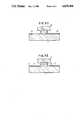
- FIG. 1A typical example of a MES type field effect transistor with the overlay type gate electrode is illustrated in FIG. 1 of the drawings.
- reference numeral 1designates a gallium-arsenide semi-insulating substrate and a gate electrode 2 of a tungsten silicide (WSi) is formed on the upper surface of the semi-insulating substrate 1.
- WSitungsten silicide
- the upper surface of the semi-insulating substratehas an exposed area on the both sides of the gate electrode 2, and the exposed area is covered with an oxide layer 3.
- a multiple metal layer 4which is longer in length than the gate electrode 2, so that the multiple metal layer 4 has an outer peripheral portion 5 projecting from the outer peripheral of the gate electrode 2.
- the multiple metal layer 4has a titanium film, a platinum film and an aurum film.
- the process of fabricating the MES type field effect transistor illustrated in FIG. 1starts with preparation of the gallium-arsenide semi-insulating substrate 1, and the gate electrode 2 is formed by a deposition of tungsten silicide followed by a lithography techniques. After formation of the gate electrode 2, the oxide layer 3 is formed on the exposed area of the semi-insulating substrate 1 so as to create a smooth topography and, thereafter, the multiple metal layer 4 is deposited and etched to form the overlay gate structure.
- the MES type field effect transistor illustrated in FIG. 1has the gate structure with a low resistance by virtue of the multiple metal layer 4, however a problem is encountered in a large parasitic capacitance due to direct contact with the oxide layer 3.
- the MES type field effect transistor illustrated in FIG. 2comprises a semi-insulating substrate 11, a gate electrode 12 formed on the upper surface of the semi-insulating substrate 11, a conductive metal layer 13 provided on the gate electrode 12, and a thin insulating film 14.
- the metal layer 13is longer in length than the gate electrode 12 so that the metal layer 13 has an outer peripheral portion 15 projecting from the outer peripheral of the gate electrode 12.
- the process of fabricationstarts with preparation of the semi-insulating substrate 11, and the gate electrode 12 is formed on the semi-insulating substrate 11. After the gate electrode 12 is formed on the upper surface of the semi-insulating substrate 11, an oxide film (not shown ) is deposited to create a smooth topography.
- the formation of the conductive metal layer 13follows, and, thereafter, the oxide film is etched away to expose the upper surface of the semi-insulating substrate 11.
- the thin insulating film 14is deposited on the exposed upper surface of the semi-insulating substrate 11 for protection.
- the metal layer with the outer peripheral portion 15has been already formed on the gate electrode 12, so that the thin insulating film 14 hardly covers the entire exposed upper surface under the outer peripheral portion 15.
- the MES type field effect transistor illustrated in FIG. 2has an exposed area under the outer peripheral portion 15 of the metal layer 13 even if the thin insulating film 14 is applied to the upper surface of the semi-insulating substrate 11.
- the MES structure illustrated in FIG. 2is free from the large parasitic capacitance, however another problem is encountered in the MES structure illustrated in FIG. 2 in incomplete protection film of the upper surface of the semi-insulating substrate 11.
- the present inventionproposes to cover an exposed area of the upper surface of the substrate with a protection film formed before formation of a thick filling layer for creating a smooth topography.
- a metal-semiconductor type field effect transistorcomprising, (a) a semi-insulating substrate with a surface having a gate forming area and a remaining area, (b) a gate electrode formed on the gate forming area of the surface of the semi-insulating substrate and having side wall, (c) a protection film formed on the side walls of the gate electrode and the remaining area of the surface of the semi-insulating substrate, and (d) a conductive layer formed on the gate electrode and having an outer peripheral portion projecting from an outer peripheral of the gate electrode.
- the semi-insulating substratemay be formed of a gallium-arsenide compound semiconductor
- the gate electrodemay be formed of a tungsten silicide.
- the protection filmis formed by a silicon nitride film with a thickness of about 1000 angstroms
- the conductive layerhas a multiple metal structure formed of titanium, platinum and aurum.
- the multiple structuremay have three metal films formed of titanium, platinum and aurum, respectively, and having thicknesses of about 500 angstroms, 200 angstroms and 400 angstroms, respectively.
- a process of fabricating a metal-semiconductor type field effect transistorcomprising the steps of (a) preparing a semi-insulating substrate with a surface having a gate forming area and a remaining area, (b) forming a gate electrode on the gate forming area of the surface of the semi-insulating substrate, the gate electrode having an upper surface and side walls, (c) forming a protection film on the upper surface and the side walls of the gate electrode and the remaining area of the surface of the semi-insulating substrate, (d) covering the protection film with a material which is different in etching rate from the protection film, (e) forming a filling layer of the material for creating a generally smooth topography by removing a part of the material over the gate electrode and a part of the protection film on the upper surface of the gate electrode, the filling layer having an upper surface substantially coplanar to the upper surface of the gate electrode, (f) forming a conductive layer on the upper surface of the gate electrode
- the protection filmis formed by a silicon nitride film deposited by using a plasma-assisted chemical vapor deposition technique, and the protection film is covered with the material by a spin coating technique using a silicon oxide in solution.
- the silicon oxidemay be dissolved in an organic solvent.
- the generally smooth topographyis created by a dry etching technique using a CF 4 -containing gaseous mixture.
- the filling layermay be removed by a wet etching technique using an etching solution containing hydrofluoric acid, and the etching solution may contain hydrofluoric acid diluted with water so as to have a hydrofluoric-acid/water ratio about 1:30.
- the protection filmis formed by a silicon nitride film deposited by a photo-excited chemical vapor deposition technique, and the material is formed of polymide resin.
- the polymide resinmay be partially removed by a dry etching technique using a CF 4 --O 2 gaseous mixture, and, thereafter, the protection film of silicon nitride may be partially removed by a dry etching technique using a CF 4 etching gas, thereby forming the filling layer.
- the polymide resinmay be removed in an oxygen plasma so as to space the conductive layer from the protection film on the semi-insulating substrate.
- FIG. 1is a cross sectional view showing the structure of a prior-art MES type field effect transistor with a overlay gate structure
- FIG. 2is a cross sectional view showing the structure of another prior-art MES type field effect transistor with a overlay gate structure which is proposed to overcome the problem encountered in the MES type field effect transistor illustrated in FIG. 1;
- FIGS. 3A to 3Gare cross sectional views showing a series of process steps for fabricating a MES type field effect transistor with a overlay gate structure according to the present invention.
- the starting materialis a gallium-arsenide (GaAs) semi-insulating substrate 21, and tungsten silicide (WSi) is deposited on a surface of the semi-insulating substrate 21 by using, for example, a sputtering technique.
- tungsten silicide layer(not shown) is deposited to a thickness of about 5000 angstroms, a mask is applied thereon and, then, the tungsten silicide layer is partially removed by an etching process.
- a gate electrode 22is formed on the semi-insulating substrate 21, and, upon completion of the gate electrode 22, an exposed area extends on the both sides of the gate electrode 22.
- silicon nitrideis deposited on the entire surface of the resultant structure, namely an upper surface and side walls of the gate electrode 22 and the exposed area of the semi-insulating substrate 21, to a thickness of about 1000 angstroms by a plasma-assisted chemical vapor deposition technique, then a protection film 23 is provided on the gate electrode 22 and the exposed area of the semi-insulating substrate 21.
- the resultant structureis illustrated in FIG. 3A.
- a solution of a silicon oxideis spun onto the resultant structure shown in FIG. 3A, so that the resultant structure is covered with the silicon oxide.
- the silicon oxide dissolved in an organic solventis used.
- the silicon oxideis partially removed by a dry etching technique using a CF 4 --(tetrafluoric carbon)-containing gaseous mixture to exposed the protection film 23 on the upper surface of the gate electrode 22.
- the CF 4 -containing gaseous mixturealso etches the silicon nitride, so that the protection film 23 on the upper surface of the gate electrode 22 is then removed to expose the upper surface of the gate electrode 22. In this way, a filling layer 24 is formed on the protection film 23.
- a generally smooth topographyis created as will be seen from FIG. 3B.
- the filling layer 24has an upper surface substantially coplanar to the upper surface of the gate electrode 22.
- a multiple metal structureis formed on the entire surface of the resultant structure shown in FIG. 3B.
- titanium, platinum and aurumare deposited in succession by using sputtering techniques.
- the titanium film, the platinum film and the aurum filmhave thicknesses of about 500 angstroms, 200 angstroms and 400 angstroms, respectively, and, then, a photoresist mask is applied on the multiple metal structure.
- the photoresist maskthe multiple metal structure is partially removed by using an ion milling technique to form a conductive layer 25 which has a length L1 longer then the length L2 of the gate electrode 22 as will be better seen from FIG. 3C.
- the MES type field effect transistorhas a gate structure consisting of the gate electrode 22 combined with the conductive layer 25, so that the resistance of the gate structure is relatively small in value. This results in that the gate structure can propagate an electric signal without any delay.
- the filling layer 24is removed to expose the protection film 23 by a wet etching technique. Namely, the resultant structure shown in FIG. 3C is dipped into an etching solution containing hydrofluoric acid (HF) for several seconds.
- the hydrofluoric acidis diluted with water, and, in this instance, the hydrofluoric acid and the water is in the ratio 1:30.
- the filling layer 24 of the silicon oxideis etched away, and the conductive layer 25 is spaced from the protection film 23 which extends on the surface of the semi-insulating substrate.
- the protection film 23perfectly covers the surface of the semi-insulating substrate 21 and the side walls of the gate electrode 22.
- the parasitic capacitanceis drastically reduced and the electric signal on the gate structure is not affected by a time constant CR.
- the surface of the semi-insulating substrate 21is perfectly covered with the protection film 23, so that the MES type field effect transistor can operate in stable.
- the MES type field effect transistor with the overlay gate structureis illustrated in FIG. 3D.
- the protection film 23is partialy removed to form source and drain contact windows by using a lithographic technique, and, thereafter, ohmic electrodes of an Au-Ge-Ni alloy are formed in the source and drain contact windows as will be seen from FIG. 3E.
- an oxide film 28 of about 1000 angstromsis formed on the entire surface of the resultant structure shown in FIG. 3E, and the oxide film 28 is partially etched away to expose the top surfaces of the ohmic electrodes 26 and 27 by using a photo-resist mask.
- the resultant structureis illustrated in FIG. 3F of the drawings.
- titanium and aurumOn the entire surface of the resultant structure shown in FIG. 3F are subsequently deposited titanium and aurum to thicknesses of about 500 angstroms and 2000 angstroms, respectively, by sputtering techniques.
- source and drain electrodes 29 and 30are grown on the ohmic electrodes 26 and 27, respectively, by an electroplating technique using a photo-resist film as a mask.
- the photo-resist filmis stripped off and, thereafter, the multiple-layer consisting of the titanium film and the arum film is removed by an ion milling (see FIG. 3G).
- the protection film and the filling layerare formed by the silicon nitride film deposited by the plasma-assisted chemical vapor deposition technique and the silicon oxide film, however a silicon nitride film (Si 3 N 4 ) deposited by a photo-excited chemical vapor deposition technique and a polymide resin film are available for forming the protection film and the filling layer, respectively.
- a gaseous mixture of CF 4 and O 2is used for the etching process for forming the filling layer.
- the protection film of silicon nitride on the upper surface of the gate electrodeis exposed by the etching process using the CF 4 --O 2 gaseous mixture, and, thereafter, the upper surface of the gate electrode is exposed by changing the etching gas from the CF 4 --O 2 gaseous mixture to a CF 4 gas.
- the polymide resinis removed in an oxygen (O 2 ) plasma.
- the protection filmis formed by the silicon nitride film deposited by the photo-exited chemical vapor deposition as described hereinbefore, the surface of the semi-insulating substrate is less damaged in comparison with that covered with the silicon nitride film deposited by the plasma-assisted chemical vapor deposition.
- the silicon nitride film deposited by the photo-excited chemical vapor depositionis liable to be corroded by the etching solution containing the hydrofluric acid (HF), so that it is preferable to use the polymide resin film as the filling layer which can be removed by using the oxygen plasma.
Landscapes
- Engineering & Computer Science (AREA)
- Physics & Mathematics (AREA)
- Condensed Matter Physics & Semiconductors (AREA)
- General Physics & Mathematics (AREA)
- Manufacturing & Machinery (AREA)
- Computer Hardware Design (AREA)
- Microelectronics & Electronic Packaging (AREA)
- Power Engineering (AREA)
- Junction Field-Effect Transistors (AREA)
- Electrodes Of Semiconductors (AREA)
- Internal Circuitry In Semiconductor Integrated Circuit Devices (AREA)
- Formation Of Insulating Films (AREA)
Abstract
Description
Claims (11)
Applications Claiming Priority (2)
| Application Number | Priority Date | Filing Date | Title |
|---|---|---|---|
| JP61303104AJPS63155671A (en) | 1986-12-18 | 1986-12-18 | Manufacture of semiconductor device |
| JP61-303104 | 1986-12-18 |
Publications (1)
| Publication Number | Publication Date |
|---|---|
| US4839304Atrue US4839304A (en) | 1989-06-13 |
Family
ID=17916937
Family Applications (1)
| Application Number | Title | Priority Date | Filing Date |
|---|---|---|---|
| US07/134,123Expired - LifetimeUS4839304A (en) | 1986-12-18 | 1987-12-17 | Method of making a field effect transistor with overlay gate structure |
Country Status (2)
| Country | Link |
|---|---|
| US (1) | US4839304A (en) |
| JP (1) | JPS63155671A (en) |
Cited By (34)
| Publication number | Priority date | Publication date | Assignee | Title |
|---|---|---|---|---|
| US5030589A (en)* | 1987-10-22 | 1991-07-09 | Mitsubishi Denki Kabushiki Kaisha | Production method for a semiconductor device |
| US5036017A (en)* | 1988-11-29 | 1991-07-30 | Mitsubishi Denki Kabushiki Kaisha | Method of making asymmetrical field effect transistor |
| US5039621A (en)* | 1990-06-08 | 1991-08-13 | Texas Instruments Incorporated | Semiconductor over insulator mesa and method of forming the same |
| US5296728A (en)* | 1990-02-26 | 1994-03-22 | Rohm Co., Ltd. | Compound semiconductor device with different gate-source and gate-drain spacings |
| US5650342A (en)* | 1988-09-08 | 1997-07-22 | Mitsubishi Denki Kabushiki Kaisha | Method of making a field effect transistor with a T shaped polysilicon gate electrode |
| US5686325A (en)* | 1994-11-30 | 1997-11-11 | Fujitsu Limited | Method for forming MESFET having T-shaped gate electrode |
| US5702958A (en)* | 1994-08-09 | 1997-12-30 | Texas Instruments Incorporated | Method for the fabrication of bipolar transistors |
| US5856232A (en)* | 1995-11-21 | 1999-01-05 | Electronics And Telecommunications Research Institute | Method for fabricating T-shaped electrode and metal layer having low resistance |
| US6075262A (en)* | 1995-09-21 | 2000-06-13 | Fujitsu Limited | Semiconductor device having T-shaped gate electrode |
| US6239007B1 (en)* | 1999-12-10 | 2001-05-29 | Taiwan Semiconductor Manufacturing Co., Ltd. | Method of forming T-shaped gate |
| US20010034686A1 (en)* | 1997-12-10 | 2001-10-25 | Eder Jeff Scott | Method of and system for defining and measuring the real options of a commercial enterprise |
| US20020046143A1 (en)* | 1995-10-03 | 2002-04-18 | Eder Jeffrey Scott | Method of and system for evaluating cash flow and elements of a business enterprise |
| US6448163B1 (en)* | 2000-08-10 | 2002-09-10 | Advanced Micro Devices, Inc. | Method for fabricating T-shaped transistor gate |
| US20040193503A1 (en)* | 2000-10-04 | 2004-09-30 | Eder Jeff Scott | Interactive sales performance management system |
| US20040210509A1 (en)* | 1997-01-06 | 2004-10-21 | Eder Jeff Scott | Automated method of and system for identifying, measuring and enhancing categories of value for a value chain |
| US20040215522A1 (en)* | 2001-12-26 | 2004-10-28 | Eder Jeff Scott | Process optimization system |
| US20050071266A1 (en)* | 2001-02-05 | 2005-03-31 | Eder Jeff Scott | Value and risk management system |
| US20050119900A1 (en)* | 2002-06-12 | 2005-06-02 | Eder Jeff S. | Purchasing optimization system |
| US20050119922A1 (en)* | 1997-01-06 | 2005-06-02 | Eder Jeff S. | Method of and system for analyzing, modeling and valuing elements of a business enterprise |
| US20050160658A1 (en)* | 2004-01-24 | 2005-07-28 | Andrzej Buczkowski | Fishing lure |
| US20050246314A1 (en)* | 2002-12-10 | 2005-11-03 | Eder Jeffrey S | Personalized medicine service |
| US20060059028A1 (en)* | 2002-09-09 | 2006-03-16 | Eder Jeffrey S | Context search system |
| US20060101017A1 (en)* | 2004-11-08 | 2006-05-11 | Eder Jeffrey S | Search ranking system |
| US20060143115A1 (en)* | 2000-10-17 | 2006-06-29 | Eder Jeffrey S | Enterprise risk management system |
| US20060175792A1 (en)* | 2004-04-13 | 2006-08-10 | Kimir Seatpost | Adjustable Bicycle Seat Post Assembly |
| US20070011049A1 (en)* | 2005-07-09 | 2007-01-11 | Eder Jeffrey S | Intelligent, personalized commerce chain |
| US20070239581A1 (en)* | 2006-04-02 | 2007-10-11 | Eder Jeff S | A data processing framework for financial services |
| US20080071588A1 (en)* | 1997-12-10 | 2008-03-20 | Eder Jeff S | Method of and system for analyzing, modeling and valuing elements of a business enterprise |
| US20090018891A1 (en)* | 2003-12-30 | 2009-01-15 | Jeff Scott Eder | Market value matrix |
| US20090043637A1 (en)* | 2004-06-01 | 2009-02-12 | Eder Jeffrey Scott | Extended value and risk management system |
| US7523065B2 (en) | 2001-12-12 | 2009-04-21 | Asset Trust, Inc. | Risk transfer supply chain system |
| US20110140123A1 (en)* | 2004-01-16 | 2011-06-16 | Sheppard Scott T | Nitride-Based Transistors With a Protective Layer and a Low-Damage Recess |
| US20140319689A1 (en)* | 2012-08-16 | 2014-10-30 | Infineon Technologies Ag | Contact Pads with Sidewall Spacers and Method of Making Contact Pads with Sidewall Spacers |
| CN110137073A (en)* | 2019-05-14 | 2019-08-16 | 中国科学院微电子研究所 | A method for anisotropic etching patterned polyimide layer |
Citations (11)
| Publication number | Priority date | Publication date | Assignee | Title |
|---|---|---|---|---|
| EP0057558A2 (en)* | 1981-01-30 | 1982-08-11 | Fujitsu Limited | Field effect semiconductor device and method of manufacturing such a device |
| US4518629A (en)* | 1982-12-10 | 1985-05-21 | Commissariat A L'energie Atomique | Process for positioning an electrical contact hole between two interconnection lines of an integrated circuit |
| US4546540A (en)* | 1982-09-16 | 1985-10-15 | Hitachi, Ltd. | Self-aligned manufacture of FET |
| US4551905A (en)* | 1982-12-09 | 1985-11-12 | Cornell Research Foundation, Inc. | Fabrication of metal lines for semiconductor devices |
| US4599790A (en)* | 1985-01-30 | 1986-07-15 | Texas Instruments Incorporated | Process for forming a T-shaped gate structure |
| US4670090A (en)* | 1986-01-23 | 1987-06-02 | Rockwell International Corporation | Method for producing a field effect transistor |
| US4694564A (en)* | 1985-07-29 | 1987-09-22 | Takatomo Enoki | Method for the manufacture of a Schottky gate field effect transistor |
| US4700462A (en)* | 1986-10-08 | 1987-10-20 | Hughes Aircraft Company | Process for making a T-gated transistor |
| US4735913A (en)* | 1986-05-06 | 1988-04-05 | Bell Communications Research, Inc. | Self-aligned fabrication process for GaAs MESFET devices |
| US4774206A (en)* | 1986-03-19 | 1988-09-27 | Siemens Aktiengesellschaft | Method for the manufacture of a self-aligned metal contact |
| JPH117172A (en)* | 1997-06-17 | 1999-01-12 | Canon Inc | Image forming device |
- 1986
- 1986-12-18JPJP61303104Apatent/JPS63155671A/enactivePending
- 1987
- 1987-12-17USUS07/134,123patent/US4839304A/ennot_activeExpired - Lifetime
Patent Citations (11)
| Publication number | Priority date | Publication date | Assignee | Title |
|---|---|---|---|---|
| EP0057558A2 (en)* | 1981-01-30 | 1982-08-11 | Fujitsu Limited | Field effect semiconductor device and method of manufacturing such a device |
| US4546540A (en)* | 1982-09-16 | 1985-10-15 | Hitachi, Ltd. | Self-aligned manufacture of FET |
| US4551905A (en)* | 1982-12-09 | 1985-11-12 | Cornell Research Foundation, Inc. | Fabrication of metal lines for semiconductor devices |
| US4518629A (en)* | 1982-12-10 | 1985-05-21 | Commissariat A L'energie Atomique | Process for positioning an electrical contact hole between two interconnection lines of an integrated circuit |
| US4599790A (en)* | 1985-01-30 | 1986-07-15 | Texas Instruments Incorporated | Process for forming a T-shaped gate structure |
| US4694564A (en)* | 1985-07-29 | 1987-09-22 | Takatomo Enoki | Method for the manufacture of a Schottky gate field effect transistor |
| US4670090A (en)* | 1986-01-23 | 1987-06-02 | Rockwell International Corporation | Method for producing a field effect transistor |
| US4774206A (en)* | 1986-03-19 | 1988-09-27 | Siemens Aktiengesellschaft | Method for the manufacture of a self-aligned metal contact |
| US4735913A (en)* | 1986-05-06 | 1988-04-05 | Bell Communications Research, Inc. | Self-aligned fabrication process for GaAs MESFET devices |
| US4700462A (en)* | 1986-10-08 | 1987-10-20 | Hughes Aircraft Company | Process for making a T-gated transistor |
| JPH117172A (en)* | 1997-06-17 | 1999-01-12 | Canon Inc | Image forming device |
Cited By (53)
| Publication number | Priority date | Publication date | Assignee | Title |
|---|---|---|---|---|
| US5030589A (en)* | 1987-10-22 | 1991-07-09 | Mitsubishi Denki Kabushiki Kaisha | Production method for a semiconductor device |
| US5650342A (en)* | 1988-09-08 | 1997-07-22 | Mitsubishi Denki Kabushiki Kaisha | Method of making a field effect transistor with a T shaped polysilicon gate electrode |
| US5036017A (en)* | 1988-11-29 | 1991-07-30 | Mitsubishi Denki Kabushiki Kaisha | Method of making asymmetrical field effect transistor |
| US5296728A (en)* | 1990-02-26 | 1994-03-22 | Rohm Co., Ltd. | Compound semiconductor device with different gate-source and gate-drain spacings |
| US5039621A (en)* | 1990-06-08 | 1991-08-13 | Texas Instruments Incorporated | Semiconductor over insulator mesa and method of forming the same |
| US5162882A (en)* | 1990-06-08 | 1992-11-10 | Texas Instruments Incorporated | Semiconductor over insulator mesa |
| US5702958A (en)* | 1994-08-09 | 1997-12-30 | Texas Instruments Incorporated | Method for the fabrication of bipolar transistors |
| US5686325A (en)* | 1994-11-30 | 1997-11-11 | Fujitsu Limited | Method for forming MESFET having T-shaped gate electrode |
| US6075262A (en)* | 1995-09-21 | 2000-06-13 | Fujitsu Limited | Semiconductor device having T-shaped gate electrode |
| US20020046143A1 (en)* | 1995-10-03 | 2002-04-18 | Eder Jeffrey Scott | Method of and system for evaluating cash flow and elements of a business enterprise |
| US5856232A (en)* | 1995-11-21 | 1999-01-05 | Electronics And Telecommunications Research Institute | Method for fabricating T-shaped electrode and metal layer having low resistance |
| US20040210509A1 (en)* | 1997-01-06 | 2004-10-21 | Eder Jeff Scott | Automated method of and system for identifying, measuring and enhancing categories of value for a value chain |
| US20080313065A1 (en)* | 1997-01-06 | 2008-12-18 | Jeff Scott Eder | Method of and system for analyzing, modeling and valuing elements of a business enterprise |
| US20080215386A1 (en)* | 1997-01-06 | 2008-09-04 | Jeff Scott Eder | Method of and system for analyzing, modeling and valuing elements of a business enterprise |
| US20080140549A1 (en)* | 1997-01-06 | 2008-06-12 | Jeff Scott Eder | Automated method of and system for identifying, measuring and enhancing categories of value for a value chain |
| US20050119922A1 (en)* | 1997-01-06 | 2005-06-02 | Eder Jeff S. | Method of and system for analyzing, modeling and valuing elements of a business enterprise |
| US20010034686A1 (en)* | 1997-12-10 | 2001-10-25 | Eder Jeff Scott | Method of and system for defining and measuring the real options of a commercial enterprise |
| US20080071588A1 (en)* | 1997-12-10 | 2008-03-20 | Eder Jeff S | Method of and system for analyzing, modeling and valuing elements of a business enterprise |
| US6239007B1 (en)* | 1999-12-10 | 2001-05-29 | Taiwan Semiconductor Manufacturing Co., Ltd. | Method of forming T-shaped gate |
| US6448163B1 (en)* | 2000-08-10 | 2002-09-10 | Advanced Micro Devices, Inc. | Method for fabricating T-shaped transistor gate |
| US20040193503A1 (en)* | 2000-10-04 | 2004-09-30 | Eder Jeff Scott | Interactive sales performance management system |
| US20050251468A1 (en)* | 2000-10-04 | 2005-11-10 | Eder Jeff S | Process management system |
| US20060184570A1 (en)* | 2000-10-17 | 2006-08-17 | Eder Jeff S | Value impact risk transfer products |
| US20090070182A1 (en)* | 2000-10-17 | 2009-03-12 | Jeffrey Scott Eder | Organization activity management system |
| US20090132448A1 (en)* | 2000-10-17 | 2009-05-21 | Jeffrey Scott Eder | Segmented predictive model system |
| US20060143115A1 (en)* | 2000-10-17 | 2006-06-29 | Eder Jeffrey S | Enterprise risk management system |
| US8185486B2 (en) | 2000-10-17 | 2012-05-22 | Asset Trust, Inc. | Segmented predictive model system |
| US20060184449A1 (en)* | 2000-10-17 | 2006-08-17 | Eder Jeff S | A risk management system for securities |
| US20050071266A1 (en)* | 2001-02-05 | 2005-03-31 | Eder Jeff Scott | Value and risk management system |
| US7873567B2 (en) | 2001-02-05 | 2011-01-18 | Asset Trust, Inc. | Value and risk management system |
| US7523065B2 (en) | 2001-12-12 | 2009-04-21 | Asset Trust, Inc. | Risk transfer supply chain system |
| US20040215522A1 (en)* | 2001-12-26 | 2004-10-28 | Eder Jeff Scott | Process optimization system |
| US20050119900A1 (en)* | 2002-06-12 | 2005-06-02 | Eder Jeff S. | Purchasing optimization system |
| US20080027769A1 (en)* | 2002-09-09 | 2008-01-31 | Jeff Scott Eder | Knowledge based performance management system |
| US20090171740A1 (en)* | 2002-09-09 | 2009-07-02 | Jeffrey Scott Eder | Contextual management system |
| US10346926B2 (en) | 2002-09-09 | 2019-07-09 | Xenogenic Development Llc | Context search system |
| US20060059028A1 (en)* | 2002-09-09 | 2006-03-16 | Eder Jeffrey S | Context search system |
| US10719888B2 (en) | 2002-09-09 | 2020-07-21 | Xenogenic Development Limited Liability Company | Context search system |
| US20090271342A1 (en)* | 2002-12-10 | 2009-10-29 | Jeffrey Scott Eder | Personalized medicine system |
| US20050246314A1 (en)* | 2002-12-10 | 2005-11-03 | Eder Jeffrey S | Personalized medicine service |
| US20090018891A1 (en)* | 2003-12-30 | 2009-01-15 | Jeff Scott Eder | Market value matrix |
| US11316028B2 (en)* | 2004-01-16 | 2022-04-26 | Wolfspeed, Inc. | Nitride-based transistors with a protective layer and a low-damage recess |
| US20110140123A1 (en)* | 2004-01-16 | 2011-06-16 | Sheppard Scott T | Nitride-Based Transistors With a Protective Layer and a Low-Damage Recess |
| US20050160658A1 (en)* | 2004-01-24 | 2005-07-28 | Andrzej Buczkowski | Fishing lure |
| US20060175792A1 (en)* | 2004-04-13 | 2006-08-10 | Kimir Seatpost | Adjustable Bicycle Seat Post Assembly |
| US20090043637A1 (en)* | 2004-06-01 | 2009-02-12 | Eder Jeffrey Scott | Extended value and risk management system |
| US20060101017A1 (en)* | 2004-11-08 | 2006-05-11 | Eder Jeffrey S | Search ranking system |
| US20070011049A1 (en)* | 2005-07-09 | 2007-01-11 | Eder Jeffrey S | Intelligent, personalized commerce chain |
| US8498915B2 (en) | 2006-04-02 | 2013-07-30 | Asset Reliance, Inc. | Data processing framework for financial services |
| US20070239581A1 (en)* | 2006-04-02 | 2007-10-11 | Eder Jeff S | A data processing framework for financial services |
| US20140319689A1 (en)* | 2012-08-16 | 2014-10-30 | Infineon Technologies Ag | Contact Pads with Sidewall Spacers and Method of Making Contact Pads with Sidewall Spacers |
| US10049994B2 (en)* | 2012-08-16 | 2018-08-14 | Infineon Technologies Ag | Contact pads with sidewall spacers and method of making contact pads with sidewall spacers |
| CN110137073A (en)* | 2019-05-14 | 2019-08-16 | 中国科学院微电子研究所 | A method for anisotropic etching patterned polyimide layer |
Also Published As
| Publication number | Publication date |
|---|---|
| JPS63155671A (en) | 1988-06-28 |
Similar Documents
| Publication | Publication Date | Title |
|---|---|---|
| US4839304A (en) | Method of making a field effect transistor with overlay gate structure | |
| US4746628A (en) | Method for making a thin film transistor | |
| US5288660A (en) | Method for forming self-aligned t-shaped transistor electrode | |
| US20040051183A1 (en) | Method of forming self-aligned contact structure with locally etched gate conductive layer | |
| US20090315021A1 (en) | Double-masking technique for increasing fabrication yield in superconducting electronics | |
| US4977100A (en) | Method of fabricating a MESFET | |
| US5217911A (en) | Method of producing a semiconductor structure including a Schottky junction | |
| EP0259490B1 (en) | A method of producing a semiconductor device | |
| US5512518A (en) | Method of manufacture of multilayer dielectric on a III-V substrate | |
| EP0392120B1 (en) | Semiconductor device with a gate having asymmetric sidewalls, and a production method thereof | |
| US5821170A (en) | Method for etching an insulating material | |
| JP2003100775A (en) | Semiconductor device and manufacturing method thereof | |
| JP3125869B2 (en) | Method for manufacturing semiconductor device | |
| JPH0472381B2 (en) | ||
| US5237192A (en) | MESFET semiconductor device having a T-shaped gate electrode | |
| JP2551315B2 (en) | Method for manufacturing semiconductor device | |
| JP2503667B2 (en) | Method for manufacturing semiconductor device | |
| JPH0574817A (en) | Manufacture of semiconductor device | |
| JPH02199825A (en) | Manufacture of electrode | |
| JP2822956B2 (en) | Method for manufacturing compound semiconductor device | |
| JP2658884B2 (en) | Method for manufacturing semiconductor device | |
| JP3304595B2 (en) | Method for manufacturing semiconductor device | |
| JPH1065000A (en) | Formation of contact hole of semiconductor device | |
| JPS6025277A (en) | Manufacturing method of semiconductor device | |
| KR100272577B1 (en) | Method for fabricating bipolar transistor |
Legal Events
| Date | Code | Title | Description |
|---|---|---|---|
| AS | Assignment | Owner name:NEC CORPORATION, JAPAN Free format text:ASSIGNMENT OF ASSIGNORS INTEREST.;ASSIGNOR:MORIKAWA, HIROSHI;REEL/FRAME:005030/0786 Effective date:19871207 | |
| STCF | Information on status: patent grant | Free format text:PATENTED CASE | |
| FEPP | Fee payment procedure | Free format text:PAYOR NUMBER ASSIGNED (ORIGINAL EVENT CODE: ASPN); ENTITY STATUS OF PATENT OWNER: LARGE ENTITY | |
| FPAY | Fee payment | Year of fee payment:4 | |
| FEPP | Fee payment procedure | Free format text:PAYER NUMBER DE-ASSIGNED (ORIGINAL EVENT CODE: RMPN); ENTITY STATUS OF PATENT OWNER: LARGE ENTITY Free format text:PAYOR NUMBER ASSIGNED (ORIGINAL EVENT CODE: ASPN); ENTITY STATUS OF PATENT OWNER: LARGE ENTITY | |
| FPAY | Fee payment | Year of fee payment:8 | |
| FEPP | Fee payment procedure | Free format text:PAYER NUMBER DE-ASSIGNED (ORIGINAL EVENT CODE: RMPN); ENTITY STATUS OF PATENT OWNER: LARGE ENTITY | |
| FEPP | Fee payment procedure | Free format text:PAYOR NUMBER ASSIGNED (ORIGINAL EVENT CODE: ASPN); ENTITY STATUS OF PATENT OWNER: LARGE ENTITY | |
| FPAY | Fee payment | Year of fee payment:12 | |
| AS | Assignment | Owner name:NEC ELECTRONICS CORPORATION, JAPAN Free format text:ASSIGNMENT OF ASSIGNORS INTEREST;ASSIGNOR:NEC CORPORATION;REEL/FRAME:013758/0440 Effective date:20021101 |