US4837606A - Vertical MOSFET with reduced bipolar effects - Google Patents
Vertical MOSFET with reduced bipolar effectsDownload PDFInfo
- Publication number
- US4837606A US4837606AUS07/014,196US1419687AUS4837606AUS 4837606 AUS4837606 AUS 4837606AUS 1419687 AUS1419687 AUS 1419687AUS 4837606 AUS4837606 AUS 4837606A
- Authority
- US
- United States
- Prior art keywords
- region
- source
- drain
- conductivity type
- junction
- Prior art date
- Legal status (The legal status is an assumption and is not a legal conclusion. Google has not performed a legal analysis and makes no representation as to the accuracy of the status listed.)
- Expired - Lifetime
Links
Images

Classifications
- H—ELECTRICITY
- H10—SEMICONDUCTOR DEVICES; ELECTRIC SOLID-STATE DEVICES NOT OTHERWISE PROVIDED FOR
- H10D—INORGANIC ELECTRIC SEMICONDUCTOR DEVICES
- H10D30/00—Field-effect transistors [FET]
- H10D30/60—Insulated-gate field-effect transistors [IGFET]
- H10D30/64—Double-diffused metal-oxide semiconductor [DMOS] FETs
- H10D30/66—Vertical DMOS [VDMOS] FETs
- H—ELECTRICITY
- H10—SEMICONDUCTOR DEVICES; ELECTRIC SOLID-STATE DEVICES NOT OTHERWISE PROVIDED FOR
- H10D—INORGANIC ELECTRIC SEMICONDUCTOR DEVICES
- H10D30/00—Field-effect transistors [FET]
- H10D30/01—Manufacture or treatment
- H10D30/021—Manufacture or treatment of FETs having insulated gates [IGFET]
- H10D30/028—Manufacture or treatment of FETs having insulated gates [IGFET] of double-diffused metal oxide semiconductor [DMOS] FETs
- H10D30/0291—Manufacture or treatment of FETs having insulated gates [IGFET] of double-diffused metal oxide semiconductor [DMOS] FETs of vertical DMOS [VDMOS] FETs
- H—ELECTRICITY
- H10—SEMICONDUCTOR DEVICES; ELECTRIC SOLID-STATE DEVICES NOT OTHERWISE PROVIDED FOR
- H10D—INORGANIC ELECTRIC SEMICONDUCTOR DEVICES
- H10D62/00—Semiconductor bodies, or regions thereof, of devices having potential barriers
- H10D62/10—Shapes, relative sizes or dispositions of the regions of the semiconductor bodies; Shapes of the semiconductor bodies
- H10D62/17—Semiconductor regions connected to electrodes not carrying current to be rectified, amplified or switched, e.g. channel regions
- H10D62/393—Body regions of DMOS transistors or IGBTs
Definitions
- the present inventionrelates to a vertical field effect transistors (FETs) such as vertical metal oxide semiconductor FETs (MOSFETs). More particularly, the invention relates to vertical, double diffused MOSFET (VDMOS) devices having source and gate electrodes on one surface of a semiconductor wafer and a drain electrode on an opposing surface of the wafer. Furthermore, the invention relates to VDMOS devices which incorporate three or four semiconductor layers.
- FETsvertical field effect transistors
- MOSFETsvertical metal oxide semiconductor FETs
- VDMOSvertical, double diffused MOSFET
- a VDMOS deviceincorporates a semiconductor wafer in which source, body and drain regions of alternate conductivity type are disposed in series.
- the body regionis disposed adjacent to a wafer surface, and the source and drain regions are located so as to define the length and width of a channel region in the body region at that surface.
- An insulated gate electrodeis disposed on the wafer surface over the channel region.
- an appropriate voltage on the gate electrodeinverts the conductivity type of the body region in that portion of the channel region that is contiguous with the wafer surface; so as to form an inversion channel contiguous with the wafer surface.
- the remainder of the channel regioncomprises a depletion region which is associated with this inversion channel.
- the depth of the depletion region portion of the channel regionis determined by the magnitude of the voltage applied to the gate electrode, and the inversion channel permits current flow between the source and drain regions.
- device operationis described as being unipolar in nature, with electron or hole flow being selectively modulated by an applied voltage to the gate.
- a conventional VDMOS structureis further described in U.S. Pat. No. 4,145,700, POWER FIELD EFFECT TRANSISTORS, C. J. Jambotkar, Mar. 20, 1979.
- Inherent in the source/body/drain structure of a VDMOS deviceis a parasitic NPN or PNP bipolar transistor.
- this parasitic transistoris detrimental to FET performance
- various effortshave been employed so as to reduce its gain.
- An example of such an effortis described in U.S. Pat. No. 4,072,975, INSULATED GATE FIELD EFFECT TRANSISTOR, A. Ishitani, Feb. 7, 1978.
- the configuration of the present inventionwas conceived.
- the structure of the present inventionmay provide greater punchthrough protection and lower on-resistance.
- the inventioncan yield a device having a threshold voltage which is lower than that of an equivalent device not incorporating the invention.
- a semiconductor waferincludes, in series, source, body and drain regions of alternate conductivity type, such that PN junctions exist between neighboring regions.
- the length and width of a channel regionis defined in the body region at a surface of the wafer by the spacing between the source and drain regions at the wafer surface.
- the body regionfurther includes a supplementary region of similar conductivity type to the body region.
- the supplementary regionhas a relatively high areal dopant concentration and it extends laterally beneath a portion of the channel region.
- a source electrodeis disposed on one surface of the wafer and a drain electrode is disposed on an opposing surface.
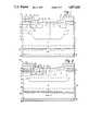
- FIG. 1is a sectional view of a conventional VDMOS device incorporating a conventional means for reducing the parasitic bipolar transistor.
- FIGS. 2 and 3are sectional views of first and second embodiments of the structure of the present invention incorporated in a VDMOS device having either three or four layers.
- FIG. 1Illustrated in FIG. 1 is a conventional N channel VDMOS device 10. It includes a semiconductor wafer 12 having opposing first and second major surfaces 14 and 16 respectively. An N type drain region 18 is disposed across the second surface 16 and extends to the first surface 14. The drain region 18 typically further comprises a planar N+ type portion 20 contiguous with the second surface 16 and an N- type extended drain portion 22 extending from the planar portion 20 to the surface 14.
- a body region 24 of P type conductivitywhich forms a body/drain PN junction 26 at its interface with the extended drain region 22.
- the body region 24might be any of a variety of geometric shapes.
- the body/drain PN junction 26might intercept the first surface 14 in the shape of a hexagon or square.
- N+ type source region 28Extending into the wafer 12 from the surface 14 within the boundary of the body/drain PN junction 26 is an N+ type source region 28.
- the source region 28forms a source/body PN junction 30 at its interface with the body region 24.
- the spacing between the source/body PN junction 30 and body/drain PN junction 26 at the first surface 14defines the length of a channel region 32 in the body region 24 at the first surface 14.
- the source region 28is ring-shaped (although not necessarily circular) and has a substantially similar shaped periphery (e.g. square or hexagonal) as the body region 24; the periphery being substantially concentric (at the first surface) with the body region 24.
- a source electrode 34contacts the source region 28 on the first surface 14, a drain electrode 36 contacts the N+type portions 20 on the second surface 16, and a gate electrode 38, spaced from the first surface 14 by a gate oxide 40, overlies the channel region 32.
- the source electrode 34is typically maintained at ground potential and the drain electrode 36 is maintained at a positive potential which might be, for example, in the 20 to 2000 volt range. So as to initiate a current flow between source and drain, a positive voltage greater than some threshold voltage is applied to the gate electrode 38. Typically the threshold voltage is in the range of approximately 1 to 5 volts.
- the device 10operates as a unipolar FET, the series nature of the source, body and drain regions 28, 24, and 18 inherently creates a parasitic NPN bipolar transistor. So as to reduce the effect of this bipolar transistor, the device 10 is provided with a P+ type body region 42 contiguous with the P type body region 24 in which the channel region is formed. The P+ type body region 42 is in ohmic contact with the source electrode 34 at the first surface 14. The presence of the P+ type body region 42 reduces the effect of the parasitic NPN bipolar transistor because it reduces the gain thereof. In an optimal conventional design, the P+ type region 42 extends laterally (i.e. in a direction parallel to the surface 14) as far as possible without extending into the channel region 32, and it is centered in the body region 24.
- the P+ type region 42extends to a depth greater than that of the body region 24 so as to form a P+/N-junction 44 at its interface with the extended drain region 22.
- a typical range of depths for the body region 24is from 2 to 4 microns, and a typical range of depths for the P+ type region 42 is from 4 to 8 microns.
- the interface between the P+ type region 42 and the body region 24is represented by a broken line 46 and is commonly referred to as a "high-low junction".
- the P+ type body regionis formed by doping and diffusing an appropriate P type dopant through an aperture in a mask on the surface 14.
- the aperture of such a maskis located such that the high-low junction 46 which is ultimately formed does not extend into the channel region 32.
- the location of the aperture which determined the location of the P+ type body region 42 in device 10is shown at 48 in FIG. 1.
- the region of peak dopant concentration within the P+ type region 42occurs at or near the surface 14 and is laterally defined by the aperture 48. Dopant concentration decreases monotonically as a function of lateral distance and depth from this region of peak dopant concentration.
- FIGS. 2 and 3An improvement over the prior art structure is shown in FIGS. 2 and 3, wherein N channel devices 50 and 150, each incorporating the present invention, are illustrated. Portions of device 150 which correspond to portions of device 50 are identified by a similar reference number preceded by the numeral 1. For clarity of description the basic features of both devices will be described with respect to device 50 only, although a similar description applies to the corresponding features of device 150. The distinctions between the devices 50 and 150 are related to the configurations of the supplementary regions 80 and 180, as elaborated upon below.
- the device 50includes a semiconductor wafer 52 having first and second opposing major surfaces 54 and 56 respectively.
- the present inventionis equally suitable to three layer and four layer structures; that portion of the wafer which is adjacent to the second surface 56 is of relatively high conductivity and may be of either N+ type or P+ type material.
- this high conductivity region, identified at 58is of N+type material and it is referred to as a high conductivity drain portion.
- the high conductivity region 58comprises a P+type region adjacent to the second surface 56; the P+type region being referred to as an anode region.
- the P+ type anode regionmay extend through the entire high conductivity region 58, or the high conductivity region 58 can comprise a P+ type anode region adjacent to the surface 56, as shown at 57, and an overlying N+ type region, as shown at 59.
- Description of such four layer (source/body/drain/anode) devicepresently referred to as a COMFET (TM of RCA Corporation), can be found in commonly assigned U.S. Pat. No. 4,364,073, POWER MOSFET WITH AN ANODE REGION, H. W. Becke et al., Dec. 14, 1982. It also should be understood that the conductivity types of all regions can be reversed, so as to yield P channel VDMOS devices of three or four layers.
- an N- type extended drain region 60Disposed on the high conductivity portion 58 and extending to the first surface 54 is an N- type extended drain region 60.
- a P type body region 62extends into the wafer from the surface 54 and forms a body/drain PN junction 64 with the N- type extended drain region 60.
- Extending into the wafer within the boundary of the body region 62is an N+ type source region 66 which forms a source/body PN junction 68 at its interface with the body region 62.
- the source/body junction 68is disposed at a predetermined depth from the surface 54 and is spaced from the body/drain junction 64 so as to define the length of a channel region 70 in the body region 62 near the first surface 54.
- the device 50 of the present inventioncan have a body region of, for example, hexagonal shape, and a hexagonal-ring shaped source region 66 having a periphery which is substantially concentric therewith.
- optimum PN junction depths as well as the conductivities of particular regionsmay be different in the device 50 compared to the conventional device 10.
- a source electrode 72contacts the source region 66 and body region 62, and a gate electrode 74 which overlies a gate insulator 76, overlies the channel region 70.
- the gate insulator 76comprises oxide and the source electrode 72 additionally contacts the body region 62.
- a drain electrode 78contacts the N+type or P+type portion of the high conductivity region 58 on the second wafer surface 56.
- the device 50incorporates a supplementary region 80 within the boundary of the body region 62.
- the supplementary region 80is of similar conductivity type to the body region 62, but it is of relatively high areal dopant concentration compared to the body region.
- the interface between the supplementary region 80 and the body region 62is a high-low junction and it is represented by dashed line 82.
- Peak dopant concentration within the supplementary region 80occurs in a region which is disposed at a substantially uniform depth from the first surface 54, as represented by the dotted line 84.
- This peak dopant concentration region 84is substantially parallel to the wafer surface 54 and is optimally located at a depth which is substantially equal to or greater than that of the source/body PN junction 68. Dopant concentration within the supplementary region 80 decreases monotonically with distance from the peak concentration region 84.
- the supplementary region 80extends laterally beneath a portion of the channel region 70, and it is desirable that this lateral extension underlie as much of the channel region as possible. In an optimum configuration the supplementary region 80 will approach but not infringe upon any portion of the channel region 70.
- the source region 66might extend to a depth of 0.4 microns from the first surface 54
- the maximum depth of the channel region 70might be 0.1-0.2 microns
- the peak concentration region 84 of the supplementary region 80might occur at a depth of 0.4-0.6 microns
- the high-low junction 82might extend laterally, beneath the channel region 70, a distance of 0.1 - 0.5 microns.
- the supplementary region 180is not entirely contained within the boundary of the body region 162.
- the region of peak dopant concentration 184is at a substantially similar or deeper depth compared to region 84 in device 50, and the supplementary region 180 extends laterally beneath the entire channel region 70.
- the contour of the body/drain PN junction 164may also have a greater lateral extent in this embodiment.
- a supplementary regioncan be provided which additionally extends the depth of the body/drain PN junction 64 or 164, and/or which includes a high-low junction 82 or 182 which intercepts the first wafer surface 54 or 154.
- the supplementary region 80 or 180is formed by ion implantation at an appropriate dosage and voltage so as to yield a peak concentration in the regions identified at 84 or 184.
- the edge of the gate electrodes 74 or 174(as well as the edges of the respective underlying and overlying materials) can be used to substantially determine the aperture location of an implantation mask, when this ion implantation is performed.
- the lateral extent of the supplementary regions 80 and 180is determined by implantation energy, dosage and species and the extent of subsequent annealing.
- the P type regions 62 or 162can be formed by selectively doping the wafer in areas not covered with the gate electrode, gate insulator, and other masking layers, and by subsequently diffusing.
- both the source region 66 or 166 and the supplementary region 80 or 180are then formed by ion implantation through the same aperture(s) in the gate electrode and gate insulator.
- boron and arsenic dopant speciesare chosen because boron diffuses at a significantly faster rate than arsenic. Additionally, boron is selected for its relatively high penetration depth (i.e. its "projected range") during ion implantation. Associated with this projected range is a lateral spreading of the implanted dose beyond the dimensions of the mask aperture through which the implantation was made. Peak concentration of the boron should be in the approximate 10 18 to 10 20 cm -3 range.
- both the source region and supplementary region implantationsare performed through the same aperture(s), they will automatically be aligned with respect to each other. It should be further noted that one can deliberately choose to not fully anneal following the boron implantation, in either sequence. If this is done, the crystallographic damage that remains can serve to further reduce carrier lifetime and mobility in the supplementary regions 80 and 180, and will serve to further reduce the gain of the parasitic bipolar transistor.
- the devices 50 and 150provide more effective suppression of the parasitic bipolar transistor than conventional devices because a P+ type portion of the body region is located closer to and underneath a portion of the channel region. Additionally, the specific location of the supplementary regions 80 and 180 provides greater punchthrough protection for the devices. Punchthrough, a well recognized and undesirable phenomenon, tends to occur at the portion of the source/body PN junctions having the smallest radius of curvature.
- the areas of small radius of curvature of the source/body PN junction 30are labeled as 88.
- the areas of small radius of curvatureare labeled as 98 and 198 respectively. These areas 88, 98 and 198 occur near the deepest portions of the source regions 28, 66 and 166.
- Punchthrough voltageis determined by the P type concentration (in an NPN structure) adjacent to the small radius of curvature areas.
- the presence of the P+ type supplementary regions 80 and 180 at these areasreduces the likelihood of punchthrough at these areas, i.e. the voltage at which punchthrough will occur is increased.
- the punchthrough voltagehas little if any dependence on the P type concentration in the body regions 62 and 162, since this relatively low conductivity portion of the respective body regions is no longer adjacent to the small radius of curvature portions of the source region.
- the P type concentration in the body region 24has to be maintained at a certain level so as to provide a punchthrough voltage greater than the source-to-drain breakdown voltage. In the device 50 of the present invention this constraint is no longer present.
- the present inventiontherefore permits the P type concentration in the body region to be reduced in the channel regions 70 and 170, thereby permitting a lower threshold voltage without sacrificing punchthrough susceptibility.
- Another potential advantage of the present inventionexists at the source electrode contact with the source region. Whereas in the conventional device 10 a portion of the source region 28 is counterdoped with P type impurities when the P+ type body region 42 is formed, this counterdoping is not present in the source regions 66 and 166 of the present invention. Thus, the resistance of the contact between source electrode 72 or 172 and the respective source region 66 or 166 in the devices 50 and 150 should be lower than the contact resistance between the source electrode 34 and the source region 28 in the device 10.
- the present inventioncan optionally be incorporated into device 10, so as to form a device with both a conventional P+ type body region 42 and a supplementary P+ type region 80 or 180. Although such a structure would not provide the indicated reduced source electrode contact resistance, it would still provide superior suppression of the parasitic bipolar transistor, enhanced punchthrough protection, and the possibility of a reduced threshold voltage.
- boronbe used as the P type source region dopant and phosphorus be used as the N type supplementary region dopant. Although these two dopant species have similar diffusion rates, phosphorus can be implanted with a greater projected range, so as to yield the desired structure, if appropriate implantation equipment and parameters are used.
Landscapes
- Insulated Gate Type Field-Effect Transistor (AREA)
Abstract
Description
Claims (5)
Priority Applications (1)
| Application Number | Priority Date | Filing Date | Title |
|---|---|---|---|
| US07/014,196US4837606A (en) | 1984-02-22 | 1987-02-12 | Vertical MOSFET with reduced bipolar effects |
Applications Claiming Priority (3)
| Application Number | Priority Date | Filing Date | Title |
|---|---|---|---|
| US06/582,601US4587713A (en) | 1984-02-22 | 1984-02-22 | Method for making vertical MOSFET with reduced bipolar effects |
| US79861285A | 1985-11-15 | 1985-11-15 | |
| US07/014,196US4837606A (en) | 1984-02-22 | 1987-02-12 | Vertical MOSFET with reduced bipolar effects |
Related Parent Applications (1)
| Application Number | Title | Priority Date | Filing Date |
|---|---|---|---|
| US79861285AContinuation | 1984-02-22 | 1985-11-15 |
Publications (1)
| Publication Number | Publication Date |
|---|---|
| US4837606Atrue US4837606A (en) | 1989-06-06 |
Family
ID=27360039
Family Applications (1)
| Application Number | Title | Priority Date | Filing Date |
|---|---|---|---|
| US07/014,196Expired - LifetimeUS4837606A (en) | 1984-02-22 | 1987-02-12 | Vertical MOSFET with reduced bipolar effects |
Country Status (1)
| Country | Link |
|---|---|
| US (1) | US4837606A (en) |
Cited By (40)
| Publication number | Priority date | Publication date | Assignee | Title |
|---|---|---|---|---|
| US4972240A (en)* | 1988-03-04 | 1990-11-20 | Nissan Motor Company, Limited | Vertical power MOS transistor |
| US4998151A (en)* | 1989-04-13 | 1991-03-05 | General Electric Company | Power field effect devices having small cell size and low contact resistance |
| US5029321A (en)* | 1988-12-19 | 1991-07-02 | Mitsubishi Denki Kabushiki Kaisha | Solid state image sensing device formed of charge coupled devices |
| US5119153A (en)* | 1989-09-05 | 1992-06-02 | General Electric Company | Small cell low contact resistance rugged power field effect devices and method of fabrication |
| US5136349A (en)* | 1989-08-30 | 1992-08-04 | Siliconix Incorporated | Closed cell transistor with built-in voltage clamp |
| US5234851A (en)* | 1989-09-05 | 1993-08-10 | General Electric Company | Small cell, low contact assistance rugged power field effect devices and method of fabrication |
| US5298770A (en)* | 1991-08-22 | 1994-03-29 | Samsung Electronics Co. Ltd. | Power switching MOS transistor |
| US5528058A (en)* | 1986-03-21 | 1996-06-18 | Advanced Power Technology, Inc. | IGBT device with platinum lifetime control and reduced gaw |
| US5550067A (en)* | 1992-03-30 | 1996-08-27 | Nippondenso Co., Ltd. | Method for producing semiconductor device having DMOS and NMOS elements formed in the same substrate |
| US5696396A (en)* | 1993-11-12 | 1997-12-09 | Nippondenso Co., Ltd. | Semiconductor device including vertical MOSFET structure with suppressed parasitic diode operation |
| US5701023A (en)* | 1994-08-03 | 1997-12-23 | National Semiconductor Corporation | Insulated gate semiconductor device typically having subsurface-peaked portion of body region for improved ruggedness |
| US5703383A (en)* | 1995-04-11 | 1997-12-30 | Kabushiki Kaisha Toshiba | Power semiconductor device |
| US5750429A (en)* | 1995-10-23 | 1998-05-12 | Toyota Jidosha Kabushiki Kaisha | Semiconductor device and manufacture method of the same |
| US5886383A (en)* | 1997-01-10 | 1999-03-23 | International Rectifier Corporation | Integrated schottky diode and mosgated device |
| US5923065A (en)* | 1996-06-12 | 1999-07-13 | Megamos Corporation | Power MOSFET device manufactured with simplified fabrication processes to achieve improved ruggedness and product cost savings |
| WO2000052750A3 (en)* | 1999-03-04 | 2001-08-09 | Infineon Technologies Ag | Method for producing a body area for a vertical mos transistor array with reduced specific starting resistor |
| US6462378B1 (en)* | 1999-01-15 | 2002-10-08 | Fairchild Korea Semiconductor, Ltd. | Power MOSFET with decreased body resistance under source region |
| WO2002084745A2 (en) | 2001-04-11 | 2002-10-24 | Silicon Wireless Corporation | Power semiconductor devices and methods of forming same |
| US20020175351A1 (en)* | 2001-04-11 | 2002-11-28 | Baliga Bantval Jayant | Power semiconductor devices having retrograded-doped transition regions that enhance breakdown voltage characteristics and methods of forming same |
| US20020185679A1 (en)* | 2000-06-23 | 2002-12-12 | Baliga Bantval Jayant | Power semiconductor devices having linear transfer characteristics and methods of forming and operating same |
| US6686604B2 (en) | 2001-09-21 | 2004-02-03 | Agere Systems Inc. | Multiple operating voltage vertical replacement-gate (VRG) transistor |
| US6690040B2 (en) | 2001-09-10 | 2004-02-10 | Agere Systems Inc. | Vertical replacement-gate junction field-effect transistor |
| US6709904B2 (en) | 2001-09-28 | 2004-03-23 | Agere Systems Inc. | Vertical replacement-gate silicon-on-insulator transistor |
| US6759730B2 (en) | 2001-09-18 | 2004-07-06 | Agere Systems Inc. | Bipolar junction transistor compatible with vertical replacement gate transistor |
| US6773994B2 (en) | 2001-12-26 | 2004-08-10 | Agere Systems Inc. | CMOS vertical replacement gate (VRG) transistors |
| US20040188737A1 (en)* | 2001-09-18 | 2004-09-30 | Samir Chaudhry | Structure and fabrication method for capacitors integratible with vertical replacement gate transistors |
| US20070284754A1 (en)* | 2006-05-12 | 2007-12-13 | Ronald Wong | Power MOSFET contact metallization |
| US20080258212A1 (en)* | 2007-04-19 | 2008-10-23 | Vishay-Siliconix | Trench metal oxide semiconductor with recessed trench material and remote contacts |
| US20090050960A1 (en)* | 2004-05-13 | 2009-02-26 | Vishay-Siliconix | Stacked Trench Metal-Oxide-Semiconductor Field Effect Transistor Device |
| US7833863B1 (en) | 2003-12-02 | 2010-11-16 | Vishay-Siliconix | Method of manufacturing a closed cell trench MOSFET |
| CN102760754A (en)* | 2012-07-31 | 2012-10-31 | 杭州士兰集成电路有限公司 | Depletion type VDMOS (Vertical Double-diffusion Metal Oxide Semiconductor) and manufacturing method thereof |
| US20130181280A1 (en)* | 2012-01-16 | 2013-07-18 | Microsemi Corporation | Pseudo self aligned radhard mosfet and process of manufacture |
| US20140110797A1 (en)* | 2012-10-18 | 2014-04-24 | Fuji Electric Co., Ltd. | Semiconductor device and method for manufacturing semiconductor device |
| US20140264343A1 (en)* | 2013-03-13 | 2014-09-18 | D3 Semiconductor LLC | Device architecture and method for temperature compensation of vertical field effect devices |
| US20150287774A1 (en)* | 2014-04-07 | 2015-10-08 | Semiconductor Components Industries, Llc | High voltage capacitor and method |
| GB2530284A (en)* | 2014-09-17 | 2016-03-23 | Anvil Semiconductors Ltd | High voltage semiconductor devices |
| US9306056B2 (en) | 2009-10-30 | 2016-04-05 | Vishay-Siliconix | Semiconductor device with trench-like feed-throughs |
| CN107958937A (en)* | 2017-11-29 | 2018-04-24 | 贵州大学 | A kind of power MOSFET device based on inverted well process and its manufacturing method |
| US9960269B2 (en)* | 2016-02-02 | 2018-05-01 | Renesas Electronics Corporation | Semiconductor device and method of manufacturing the same |
| US11901446B2 (en) | 2021-08-18 | 2024-02-13 | Unity Power Technology Limited | SiC MOSFET with transverse P+ region |
Citations (12)
| Publication number | Priority date | Publication date | Assignee | Title |
|---|---|---|---|---|
| US4055884A (en)* | 1976-12-13 | 1977-11-01 | International Business Machines Corporation | Fabrication of power field effect transistors and the resulting structures |
| US4072975A (en)* | 1976-04-29 | 1978-02-07 | Sony Corporation | Insulated gate field effect transistor |
| GB2062349A (en)* | 1979-10-30 | 1981-05-20 | Rca Corp | Mosfet |
| US4297718A (en)* | 1973-05-22 | 1981-10-27 | Semiconductor Research Foundation Mitsubishi Denki K.K. | Vertical type field effect transistor |
| US4329704A (en)* | 1978-09-20 | 1982-05-11 | Fujitsu Limited | MOS Random access memory with buried storage capacitor |
| US4344081A (en)* | 1980-04-14 | 1982-08-10 | Supertex, Inc. | Combined DMOS and a vertical bipolar transistor device and fabrication method therefor |
| US4364073A (en)* | 1980-03-25 | 1982-12-14 | Rca Corporation | Power MOSFET with an anode region |
| US4374455A (en)* | 1979-10-30 | 1983-02-22 | Rca Corporation | Method for manufacturing a vertical, grooved MOSFET |
| US4455565A (en)* | 1980-02-22 | 1984-06-19 | Rca Corporation | Vertical MOSFET with an aligned gate electrode and aligned drain shield electrode |
| US4455566A (en)* | 1979-06-18 | 1984-06-19 | Fujitsu Limited | Highly integrated semiconductor memory device |
| US4466175A (en)* | 1981-06-17 | 1984-08-21 | U.S. Philips Corporation | Manufacture of vertical insulated gate field effect transistors |
| JPH05223277A (en)* | 1992-02-13 | 1993-08-31 | Matsushita Electric Ind Co Ltd | Integral-type air conditioner |
- 1987
- 1987-02-12USUS07/014,196patent/US4837606A/ennot_activeExpired - Lifetime
Patent Citations (13)
| Publication number | Priority date | Publication date | Assignee | Title |
|---|---|---|---|---|
| US4297718A (en)* | 1973-05-22 | 1981-10-27 | Semiconductor Research Foundation Mitsubishi Denki K.K. | Vertical type field effect transistor |
| US4072975A (en)* | 1976-04-29 | 1978-02-07 | Sony Corporation | Insulated gate field effect transistor |
| US4145700A (en)* | 1976-12-13 | 1979-03-20 | International Business Machines Corporation | Power field effect transistors |
| US4055884A (en)* | 1976-12-13 | 1977-11-01 | International Business Machines Corporation | Fabrication of power field effect transistors and the resulting structures |
| US4329704A (en)* | 1978-09-20 | 1982-05-11 | Fujitsu Limited | MOS Random access memory with buried storage capacitor |
| US4455566A (en)* | 1979-06-18 | 1984-06-19 | Fujitsu Limited | Highly integrated semiconductor memory device |
| US4374455A (en)* | 1979-10-30 | 1983-02-22 | Rca Corporation | Method for manufacturing a vertical, grooved MOSFET |
| GB2062349A (en)* | 1979-10-30 | 1981-05-20 | Rca Corp | Mosfet |
| US4455565A (en)* | 1980-02-22 | 1984-06-19 | Rca Corporation | Vertical MOSFET with an aligned gate electrode and aligned drain shield electrode |
| US4364073A (en)* | 1980-03-25 | 1982-12-14 | Rca Corporation | Power MOSFET with an anode region |
| US4344081A (en)* | 1980-04-14 | 1982-08-10 | Supertex, Inc. | Combined DMOS and a vertical bipolar transistor device and fabrication method therefor |
| US4466175A (en)* | 1981-06-17 | 1984-08-21 | U.S. Philips Corporation | Manufacture of vertical insulated gate field effect transistors |
| JPH05223277A (en)* | 1992-02-13 | 1993-08-31 | Matsushita Electric Ind Co Ltd | Integral-type air conditioner |
Non-Patent Citations (4)
| Title |
|---|
| "A Highly Reliable 16 Output High Voltage NMOS/CMOS Logic IC With Shielded Source Structure", H. Wakaumi et al., IEDM, 1983, pp. 416-419. |
| "A Parasitic Effect-Free, High Voltage MOS ICs with Shielded Source Structure", H. Sakuma et al., IEDM, 1982, pp. 254-257. |
| A Highly Reliable 16 Output High Voltage NMOS/CMOS Logic IC With Shielded Source Structure , H. Wakaumi et al., IEDM, 1983, pp. 416 419.* |
| A Parasitic Effect Free, High Voltage MOS ICs with Shielded Source Structure , H. Sakuma et al., IEDM, 1982, pp. 254 257.* |
Cited By (88)
| Publication number | Priority date | Publication date | Assignee | Title |
|---|---|---|---|---|
| US5528058A (en)* | 1986-03-21 | 1996-06-18 | Advanced Power Technology, Inc. | IGBT device with platinum lifetime control and reduced gaw |
| US4972240A (en)* | 1988-03-04 | 1990-11-20 | Nissan Motor Company, Limited | Vertical power MOS transistor |
| US5029321A (en)* | 1988-12-19 | 1991-07-02 | Mitsubishi Denki Kabushiki Kaisha | Solid state image sensing device formed of charge coupled devices |
| US4998151A (en)* | 1989-04-13 | 1991-03-05 | General Electric Company | Power field effect devices having small cell size and low contact resistance |
| US5136349A (en)* | 1989-08-30 | 1992-08-04 | Siliconix Incorporated | Closed cell transistor with built-in voltage clamp |
| US5119153A (en)* | 1989-09-05 | 1992-06-02 | General Electric Company | Small cell low contact resistance rugged power field effect devices and method of fabrication |
| US5234851A (en)* | 1989-09-05 | 1993-08-10 | General Electric Company | Small cell, low contact assistance rugged power field effect devices and method of fabrication |
| US5298770A (en)* | 1991-08-22 | 1994-03-29 | Samsung Electronics Co. Ltd. | Power switching MOS transistor |
| US5550067A (en)* | 1992-03-30 | 1996-08-27 | Nippondenso Co., Ltd. | Method for producing semiconductor device having DMOS and NMOS elements formed in the same substrate |
| US5696396A (en)* | 1993-11-12 | 1997-12-09 | Nippondenso Co., Ltd. | Semiconductor device including vertical MOSFET structure with suppressed parasitic diode operation |
| US5701023A (en)* | 1994-08-03 | 1997-12-23 | National Semiconductor Corporation | Insulated gate semiconductor device typically having subsurface-peaked portion of body region for improved ruggedness |
| US5897355A (en)* | 1994-08-03 | 1999-04-27 | National Semiconductor Corporation | Method of manufacturing insulated gate semiconductor device to improve ruggedness |
| US5703383A (en)* | 1995-04-11 | 1997-12-30 | Kabushiki Kaisha Toshiba | Power semiconductor device |
| US5750429A (en)* | 1995-10-23 | 1998-05-12 | Toyota Jidosha Kabushiki Kaisha | Semiconductor device and manufacture method of the same |
| US6034398A (en)* | 1995-10-23 | 2000-03-07 | Toyota Jidosha Kabushiki Kaisha | Semiconductor device and manufacturing method of the same |
| US5923065A (en)* | 1996-06-12 | 1999-07-13 | Megamos Corporation | Power MOSFET device manufactured with simplified fabrication processes to achieve improved ruggedness and product cost savings |
| US5886383A (en)* | 1997-01-10 | 1999-03-23 | International Rectifier Corporation | Integrated schottky diode and mosgated device |
| US6462378B1 (en)* | 1999-01-15 | 2002-10-08 | Fairchild Korea Semiconductor, Ltd. | Power MOSFET with decreased body resistance under source region |
| WO2000052750A3 (en)* | 1999-03-04 | 2001-08-09 | Infineon Technologies Ag | Method for producing a body area for a vertical mos transistor array with reduced specific starting resistor |
| US6670244B2 (en) | 1999-03-04 | 2003-12-30 | Infineon Technologies Ag | Method for fabricating a body region for a vertical MOS transistor arrangement having a reduced on resistivity |
| EP2261961A2 (en) | 1999-03-04 | 2010-12-15 | Infineon Technologies AG | Method of making a vertical MOS transistor device |
| US20050001268A1 (en)* | 2000-06-23 | 2005-01-06 | Baliga Bantval Jayant | Power semiconductor devices having linear transfer characteristics when regions therein are in velocity saturation modes and methods of forming and operating same |
| US6784486B2 (en) | 2000-06-23 | 2004-08-31 | Silicon Semiconductor Corporation | Vertical power devices having retrograded-doped transition regions therein |
| US20020185679A1 (en)* | 2000-06-23 | 2002-12-12 | Baliga Bantval Jayant | Power semiconductor devices having linear transfer characteristics and methods of forming and operating same |
| EP2362423A3 (en)* | 2001-04-11 | 2012-01-04 | Silicon Semiconductor Corporation | Vertical power semiconductor device and method of making the same |
| US20020175351A1 (en)* | 2001-04-11 | 2002-11-28 | Baliga Bantval Jayant | Power semiconductor devices having retrograded-doped transition regions that enhance breakdown voltage characteristics and methods of forming same |
| KR100869324B1 (en) | 2001-04-11 | 2008-11-18 | 실리콘 세미컨덕터 코포레이션 | Power semiconductor device with side extension base shielding area to prevent base rich-through and manufacturing method thereof |
| WO2002084745A2 (en) | 2001-04-11 | 2002-10-24 | Silicon Wireless Corporation | Power semiconductor devices and methods of forming same |
| US20040099905A1 (en)* | 2001-04-11 | 2004-05-27 | Baliga Bantval Jayant | Power semiconductor devices having laterally extending base shielding regions that inhibit base reach-through and schottky rectifying flyback diodes |
| US7041559B2 (en) | 2001-04-11 | 2006-05-09 | Silicon Semiconductor Corporation | Methods of forming power semiconductor devices having laterally extending base shielding regions |
| US20050032291A1 (en)* | 2001-04-11 | 2005-02-10 | Baliga Bantval Jayant | Methods of forming power semiconductor devices having laterally extending base shielding regions |
| EP2362422A3 (en)* | 2001-04-11 | 2012-01-04 | Silicon Semiconductor Corporation | Vertical power semiconductor device and method of making the same |
| WO2002084745A3 (en)* | 2001-04-11 | 2003-08-21 | Silicon Wireless Corp | Power semiconductor devices and methods of forming same |
| US6781194B2 (en) | 2001-04-11 | 2004-08-24 | Silicon Semiconductor Corporation | Vertical power devices having retrograded-doped transition regions and insulated trench-based electrodes therein |
| US20020177277A1 (en)* | 2001-04-11 | 2002-11-28 | Baliga Bantval Jayant | Power semiconductor devices having laterally extending base shielding regions that inhibit base reach through and methods of forming same |
| US6791143B2 (en) | 2001-04-11 | 2004-09-14 | Silicon Semiconductor Corporation | Power semiconductor devices having laterally extending base shielding regions that inhibit base reach-through |
| US20040232479A1 (en)* | 2001-04-11 | 2004-11-25 | Baliga Bantval Jayant | Methods of forming vertical power devices having trench-based source electrodes with sidewall source contacts |
| US6800897B2 (en) | 2001-04-11 | 2004-10-05 | Silicon Semiconductor Corporation | Integrated circuit power devices having junction barrier controlled schottky diodes therein |
| US7033877B2 (en) | 2001-09-10 | 2006-04-25 | Agere Systems Inc. | Vertical replacement-gate junction field-effect transistor |
| US6690040B2 (en) | 2001-09-10 | 2004-02-10 | Agere Systems Inc. | Vertical replacement-gate junction field-effect transistor |
| US20060166429A1 (en)* | 2001-09-10 | 2006-07-27 | Samir Chaudhry | Vertical replacement-gate junction field-effect transistor |
| US20040110345A1 (en)* | 2001-09-10 | 2004-06-10 | Samir Chaudhry | Vertical replacement-gate junction field-effect transistor |
| US7491610B2 (en) | 2001-09-18 | 2009-02-17 | Agere Systems Inc. | Fabrication method |
| US7700432B2 (en) | 2001-09-18 | 2010-04-20 | Agere Systems Inc. | Method of fabricating a vertical transistor and capacitor |
| US20040188737A1 (en)* | 2001-09-18 | 2004-09-30 | Samir Chaudhry | Structure and fabrication method for capacitors integratible with vertical replacement gate transistors |
| US20100044767A1 (en)* | 2001-09-18 | 2010-02-25 | Agere Systems Inc. | Structure and fabrication method for capacitors integratible with vertical replacement gate transistors |
| US6759730B2 (en) | 2001-09-18 | 2004-07-06 | Agere Systems Inc. | Bipolar junction transistor compatible with vertical replacement gate transistor |
| US7242056B2 (en) | 2001-09-18 | 2007-07-10 | Agere Systems Inc. | Structure and fabrication method for capacitors integratible with vertical replacement gate transistors |
| US20070228440A1 (en)* | 2001-09-18 | 2007-10-04 | Agere Systems Inc. | Structure and fabrication method for capacitors integratible with vertical replacement gate transistors |
| US20070238243A1 (en)* | 2001-09-18 | 2007-10-11 | Agere Systems Inc. | Fabrication method |
| US7633118B2 (en) | 2001-09-18 | 2009-12-15 | Agere Systems Inc. | Structure and fabrication method for capacitors integratible with vertical replacement gate transistors |
| US20090130810A1 (en)* | 2001-09-18 | 2009-05-21 | Agere Systems Inc. | Fabrication method |
| US7911006B2 (en) | 2001-09-18 | 2011-03-22 | Agere Systems Inc. | Structure and fabrication method for capacitors integratible with vertical replacement gate transistors |
| US7056783B2 (en) | 2001-09-21 | 2006-06-06 | Agere Systems Inc. | Multiple operating voltage vertical replacement-gate (VRG) transistor |
| US20050048709A1 (en)* | 2001-09-21 | 2005-03-03 | Layman Paul Arthur | Multiple operating voltage vertical replacement-gate (VRG) transistor |
| US6686604B2 (en) | 2001-09-21 | 2004-02-03 | Agere Systems Inc. | Multiple operating voltage vertical replacement-gate (VRG) transistor |
| US7078280B2 (en) | 2001-09-28 | 2006-07-18 | Agere Systems Inc. | Vertical replacement-gate silicon-on-insulator transistor |
| US20040155264A1 (en)* | 2001-09-28 | 2004-08-12 | Samir Chaudhry | Vertical replacement-gate silicon-on-insulator transistor |
| US6709904B2 (en) | 2001-09-28 | 2004-03-23 | Agere Systems Inc. | Vertical replacement-gate silicon-on-insulator transistor |
| US6773994B2 (en) | 2001-12-26 | 2004-08-10 | Agere Systems Inc. | CMOS vertical replacement gate (VRG) transistors |
| US7833863B1 (en) | 2003-12-02 | 2010-11-16 | Vishay-Siliconix | Method of manufacturing a closed cell trench MOSFET |
| US8183629B2 (en) | 2004-05-13 | 2012-05-22 | Vishay-Siliconix | Stacked trench metal-oxide-semiconductor field effect transistor device |
| US20090050960A1 (en)* | 2004-05-13 | 2009-02-26 | Vishay-Siliconix | Stacked Trench Metal-Oxide-Semiconductor Field Effect Transistor Device |
| US8697571B2 (en) | 2006-05-12 | 2014-04-15 | Vishay-Siliconix | Power MOSFET contact metallization |
| US20070284754A1 (en)* | 2006-05-12 | 2007-12-13 | Ronald Wong | Power MOSFET contact metallization |
| US8471390B2 (en) | 2006-05-12 | 2013-06-25 | Vishay-Siliconix | Power MOSFET contact metallization |
| US20080258212A1 (en)* | 2007-04-19 | 2008-10-23 | Vishay-Siliconix | Trench metal oxide semiconductor with recessed trench material and remote contacts |
| US8368126B2 (en) | 2007-04-19 | 2013-02-05 | Vishay-Siliconix | Trench metal oxide semiconductor with recessed trench material and remote contacts |
| US8883580B2 (en) | 2007-04-19 | 2014-11-11 | Vishay-Siliconix | Trench metal oxide semiconductor with recessed trench material and remote contacts |
| US9306056B2 (en) | 2009-10-30 | 2016-04-05 | Vishay-Siliconix | Semiconductor device with trench-like feed-throughs |
| US10032901B2 (en) | 2009-10-30 | 2018-07-24 | Vishay-Siliconix | Semiconductor device with trench-like feed-throughs |
| US8841718B2 (en)* | 2012-01-16 | 2014-09-23 | Microsemi Corporation | Pseudo self aligned radhard MOSFET and process of manufacture |
| US20130181280A1 (en)* | 2012-01-16 | 2013-07-18 | Microsemi Corporation | Pseudo self aligned radhard mosfet and process of manufacture |
| CN102760754A (en)* | 2012-07-31 | 2012-10-31 | 杭州士兰集成电路有限公司 | Depletion type VDMOS (Vertical Double-diffusion Metal Oxide Semiconductor) and manufacturing method thereof |
| CN102760754B (en)* | 2012-07-31 | 2015-07-15 | 杭州士兰集成电路有限公司 | Depletion type VDMOS (Vertical Double-diffusion Metal Oxide Semiconductor) and manufacturing method thereof |
| US20140110797A1 (en)* | 2012-10-18 | 2014-04-24 | Fuji Electric Co., Ltd. | Semiconductor device and method for manufacturing semiconductor device |
| US9608057B2 (en) | 2012-10-18 | 2017-03-28 | Fuji Electric Co., Ltd. | Semiconductor device and method for manufacturing semiconductor device |
| US9331194B2 (en)* | 2012-10-18 | 2016-05-03 | Fuji Electric Co., Ltd. | Semiconductor device and method for manufacturing semiconductor device |
| WO2014160453A3 (en)* | 2013-03-13 | 2014-11-27 | D3 Semiconductor LLC | Device architecture and method for temperature compensation of vertical field effect devices |
| US20140264343A1 (en)* | 2013-03-13 | 2014-09-18 | D3 Semiconductor LLC | Device architecture and method for temperature compensation of vertical field effect devices |
| US20150287774A1 (en)* | 2014-04-07 | 2015-10-08 | Semiconductor Components Industries, Llc | High voltage capacitor and method |
| US10411086B2 (en)* | 2014-04-07 | 2019-09-10 | Semiconductor Components Industries, Llc | High voltage capacitor and method |
| US11018216B2 (en) | 2014-04-07 | 2021-05-25 | Semiconductor Components Industries, Llc | High voltage capacitor and method |
| GB2530284A (en)* | 2014-09-17 | 2016-03-23 | Anvil Semiconductors Ltd | High voltage semiconductor devices |
| US10157979B2 (en) | 2014-09-17 | 2018-12-18 | Anvil Semiconductors Limited | High voltage semiconductor device with reduced peak electric field in active and termination areas of the device |
| US9960269B2 (en)* | 2016-02-02 | 2018-05-01 | Renesas Electronics Corporation | Semiconductor device and method of manufacturing the same |
| CN107958937A (en)* | 2017-11-29 | 2018-04-24 | 贵州大学 | A kind of power MOSFET device based on inverted well process and its manufacturing method |
| US11901446B2 (en) | 2021-08-18 | 2024-02-13 | Unity Power Technology Limited | SiC MOSFET with transverse P+ region |
Similar Documents
| Publication | Publication Date | Title |
|---|---|---|
| US4837606A (en) | Vertical MOSFET with reduced bipolar effects | |
| US4587713A (en) | Method for making vertical MOSFET with reduced bipolar effects | |
| US5264719A (en) | High voltage lateral semiconductor device | |
| US5268586A (en) | Vertical power MOS device with increased ruggedness and method of fabrication | |
| US5614751A (en) | Edge termination structure for power MOSFET | |
| US4639762A (en) | MOSFET with reduced bipolar effects | |
| US6091086A (en) | Reverse blocking IGBT | |
| US5933733A (en) | Zero thermal budget manufacturing process for MOS-technology power devices | |
| US5893736A (en) | Methods of forming insulated gate semiconductor devices having spaced epitaxial JFET regions therein | |
| US4605948A (en) | Semiconductor structure for electric field distribution | |
| US7238987B2 (en) | Lateral semiconductor device and method for producing the same | |
| KR910020923A (en) | Power transistor device and manufacturing method | |
| JPH09232567A (en) | MOS gate power device and manufacturing method thereof | |
| US5879967A (en) | Methods forming power semiconductor devices having latch-up inhibiting regions | |
| US7622741B2 (en) | Semiconductor device and method for manufacturing same | |
| US20250107166A1 (en) | Semiconductor device and manufacturing method of semiconductor device | |
| US5770880A (en) | P-collector H.V. PMOS switch VT adjusted source/drain | |
| US4975751A (en) | High breakdown active device structure with low series resistance | |
| US5874338A (en) | MOS-technology power device and process of making same | |
| JP2000509916A (en) | Semiconductor device controllable by electric field effect | |
| US6501128B1 (en) | Insulated gate transistor and the method of manufacturing the same | |
| JP3409244B2 (en) | Semiconductor device | |
| GB2165091A (en) | IGFET and method for fabricating same | |
| JP3437967B2 (en) | Power FET with reduced threshold voltage | |
| US5912491A (en) | MOS device |
Legal Events
| Date | Code | Title | Description |
|---|---|---|---|
| AS | Assignment | Owner name:GENERAL ELECTRIC COMPANY Free format text:MERGER;ASSIGNOR:R C A CORPORATION, A CORP. OF DE.;REEL/FRAME:004837/0618 Effective date:19880129 Owner name:GENERAL ELECTRIC COMPANY,STATELESS Free format text:MERGER;ASSIGNOR:R C A CORPORATION, A CORP. OF DE.;REEL/FRAME:004837/0618 Effective date:19880129 | |
| FEPP | Fee payment procedure | Free format text:PAYOR NUMBER ASSIGNED (ORIGINAL EVENT CODE: ASPN); ENTITY STATUS OF PATENT OWNER: LARGE ENTITY | |
| STCF | Information on status: patent grant | Free format text:PATENTED CASE | |
| FEPP | Fee payment procedure | Free format text:PAYER NUMBER DE-ASSIGNED (ORIGINAL EVENT CODE: RMPN); ENTITY STATUS OF PATENT OWNER: LARGE ENTITY | |
| REFU | Refund | Free format text:REFUND OF EXCESS PAYMENTS PROCESSED (ORIGINAL EVENT CODE: R169); ENTITY STATUS OF PATENT OWNER: LARGE ENTITY | |
| FPAY | Fee payment | Year of fee payment:4 | |
| REFU | Refund | Free format text:REFUND OF EXCESS PAYMENTS PROCESSED (ORIGINAL EVENT CODE: R169); ENTITY STATUS OF PATENT OWNER: LARGE ENTITY | |
| FEPP | Fee payment procedure | Free format text:PAYOR NUMBER ASSIGNED (ORIGINAL EVENT CODE: ASPN); ENTITY STATUS OF PATENT OWNER: LARGE ENTITY | |
| FPAY | Fee payment | Year of fee payment:8 | |
| AS | Assignment | Owner name:INTERSIL CORPORATION, FLORIDA Free format text:ASSIGNMENT OF ASSIGNORS INTEREST;ASSIGNOR:HARRIS CORPORATION;REEL/FRAME:010255/0405 Effective date:19990813 | |
| AS | Assignment | Owner name:CREDIT SUISSE FIRST BOSTON, AS COLLATERAL AGENT, N Free format text:SECURITY INTEREST;ASSIGNOR:INTERSIL CORPORATION;REEL/FRAME:010351/0410 Effective date:19990813 | |
| FPAY | Fee payment | Year of fee payment:12 | |
| AS | Assignment | Owner name:INTERSIL HOLDING CORPORATION, CALIFORNIA Free format text:INTELLECTUAL PROPERTY PARTIAL RELEASE;ASSIGNOR:CREIDT SUISSE FIRST BOSTON;REEL/FRAME:011667/0166 Effective date:20010303 | |
| AS | Assignment | Owner name:FAIRCHILD SEMICONDUCTOR CORPORATION, MAINE Free format text:REASSIGNMENT OF PATENT APPLICATIONS;ASSIGNOR:INTERSIL CORPORATION;REEL/FRAME:012002/0206 Effective date:20010406 |