US4837496A - Low voltage current source/start-up circuit - Google Patents
Low voltage current source/start-up circuitDownload PDFInfo
- Publication number
- US4837496A US4837496AUS07/173,758US17375888AUS4837496AUS 4837496 AUS4837496 AUS 4837496AUS 17375888 AUS17375888 AUS 17375888AUS 4837496 AUS4837496 AUS 4837496A
- Authority
- US
- United States
- Prior art keywords
- transistor
- resistor
- current
- transistors
- currents
- Prior art date
- Legal status (The legal status is an assumption and is not a legal conclusion. Google has not performed a legal analysis and makes no representation as to the accuracy of the status listed.)
- Expired - Lifetime
Links
Images

Classifications
- G—PHYSICS
- G05—CONTROLLING; REGULATING
- G05F—SYSTEMS FOR REGULATING ELECTRIC OR MAGNETIC VARIABLES
- G05F3/00—Non-retroactive systems for regulating electric variables by using an uncontrolled element, or an uncontrolled combination of elements, such element or such combination having self-regulating properties
- G05F3/02—Regulating voltage or current
- G05F3/08—Regulating voltage or current wherein the variable is DC
- G05F3/10—Regulating voltage or current wherein the variable is DC using uncontrolled devices with non-linear characteristics
- G05F3/16—Regulating voltage or current wherein the variable is DC using uncontrolled devices with non-linear characteristics being semiconductor devices
- G05F3/20—Regulating voltage or current wherein the variable is DC using uncontrolled devices with non-linear characteristics being semiconductor devices using diode- transistor combinations
Definitions
- This inventionrelates generally to current source circuits, and more particularly the invention relates to a current source circuit which can be operated from a low-voltage variable power supply and is independent of power supply voltage and start-up currents.
- a current source circuittypically has a high output impedance but produces current which is not necessarily independent of the power supply voltage.
- Dobkin U.S. Pat. No. 3,930,172discloses a circuit which is independent of power supply. As described in the patent, a first pair of transistors is connected in series with one another between the supply and a second pair of transistors is connected in series with one another between the supply. The base-emitter junctions of the transistors are connected in a series loop, such that a voltage is developed between the base-emitter junctions of two adjacent transistors which is equal to the base-emitter voltage summation. The base-emitter voltages of any series-connected transistors oppose one another in the series loop.
- the Dobkin circuitrequires voltage equal to two base-emitter voltage drops (V BE ) for minimum operation. The output resistance is actually negative.
- Taylor U.S. Pat. No. 4,574,233discloses a circuit including a first transistor having an output current which is sensed across a resistance connected between the emitter of the first transistor and the negative side of a supply voltage.
- a series-negative feedback loopcomprising two transistors is connected between the emitter of the first transistor and the base of the first transistor.
- the three transistors and the other circuit componentsare selected to result in an incremental output resistance approaching that of a cascode current source, while having a voltage drop across the circuit of substantially less than one volt.
- the output current through the first transistoris dependent on input currents through the pair of transistors which are in turn dependent on the power supply.
- An object of the present inventionis an improved start-up circuit/current source whose operation is independent of power supply.
- Another object of the inventionis a circuit which operates from a power supply having a voltage as low as a single base-emitter voltage drop (V BE ).
- a feature of the inventionis the use of two equal start-up currents and feedback circuitry whereby two current sources operate independently of the start-up current magnitudes and the magnitude of the start-up currents does not have to be accurately controlled.
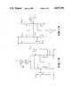
- FIG. 1is a schematic of a start-up circuit/current source in accordance with one embodiment of the invention.
- FIG. 2is a schematic of a start-up circuit/current source in accordance with another embodiment of the invention.
- FIG. 3is a schematic of a start-up circuit/current source in accordance with still another embodiment of the invention.
- FIG. 4is a schematic of another embodiment of the start-up circuit/current source of FIGS. 2 and 3 but using opposite conductivity-type bipolar transistors.
- FIG. 1is a schematic of a start-up circuit/current source in accordance with one embodiment of the invention in which two current sources, I 01 and I 02 , are provided using two start-up FET currents, I J1 and I J2 .
- the magnitude of I 01 and I 02is independent of I J1 and I J2 and the power supply voltage V+.
- the total supply voltage(V+ to ground) does not have to be more than a base-emitter voltage drop (for transistors Q1 and Q3) plus a small resistive drop across a resistor R3, and a small saturation voltage across FETs J1 or J2.
- FIG. 1is similar to the circuit of U.S. Pat. No. 4,574,233, supra. However, the patented circuit produces an output current which is a function of start-up currents and thus a function of the power supply voltage, whereas the circuit of FIG. 1 produces an output current which is independent of power supply voltage. This is accomplished by making the two start-up currents equal and having the emitter areas of Q3 and Q4 unequal as will be described below.
- the magnitude of FET currents of J1 and J2is difficult to control, but they can be made equal.
- the FETscan be operated in the pinched-off region or in the linear (resistive) region. In fact, the two FETs can be replaced by two equal value resistors.
- the start-up current I J1is provided through the serial circuit comprising FET J1, resistor R1, NPN transistor Q4, and resistor R4 between V+ and ground.
- the start-up current I J2is provided through the serial circuit comprising FET J2, NPN transistor Q3 (having shorted collector and base), and resistor R3 from V+ to ground. The bases of transistors Q3 and Q4 are connected.
- the current source I 01is provided through NPN transistor Q1 (having a base bias provided by the start-up current I J1 ) and the series resistor R3.
- the current source I 02is provided through NPN transistor Q2 (having a base bias generated by start-up current I J1 ) and a series resistor R2. Resistors R1, R3 and R4 are equal in resistance to a value R.
- the output resistance of current source I 01is extremely high and effectively the output resistance of a common-base configured transistor.
- the base voltage of transistor Q1 with respect to ground, however,is a function of I J2 flowing through resistor R3.
- the output resistance of current source I 02is not as high as the output resistance of current source I 01 since transistor Q2 is in a common-emitter configuration degenerated by R2. However, the base voltage of transistor Q2 is independent of start-up FET currents I J1 and I J2 .
- the output impedance of Q1is high because as the collector voltage of Q1 is increased, and its base-emitter voltage is reduced due to the Early effect, the current I 01 , which is not a function of V BEQ1 , will not change.
- the output impedance of current source I 02is not as high as the I 01 output impedance because I 02 is dependent on V BEQ2 , which reduces due to increasing collector voltage on Q2.
- the collector voltage of Q2tracks the collector voltage of Q1
- the V BE variations in Q1 and Q2 due to the Early effectwill be equal in equation (4), and the effective output resistance of I 02 will be high.
- circuit of FIG. 1can be simplified by shorting out R1 and deleting Q2 and R2.
- FETs J1 and J2can be replaced by matched resistors; the absolute value of the current I, through the resistors, will vary significantly with supply voltage, but as long as the two currents match, the above equations will be satisfied.
- V BEbase-emitter voltage
- J3FET
- FIG. 4is a schematic of another embodiment in which PNP (sourcing) transistor current sources are achieved by replacing the NPN transistors Q1, Q2, Q3, and Q4 by PNP transistors. Emitter scaling is then achieved by emitter periphery and not by emitter area ratioing. Transistor Q5 and transistor Q6 of FIGS. 2 and 3 are replaced by two matched NPN transistors Q7, Q8.
Landscapes
- Engineering & Computer Science (AREA)
- Physics & Mathematics (AREA)
- Microelectronics & Electronic Packaging (AREA)
- Nonlinear Science (AREA)
- Electromagnetism (AREA)
- General Physics & Mathematics (AREA)
- Radar, Positioning & Navigation (AREA)
- Automation & Control Theory (AREA)
- Control Of Electrical Variables (AREA)
Abstract
Description
I.sub.J1 =I.sub.J2 =I
IR.sub.3 +I.sub.01 R.sub.3 +V.sub.BEQ1 =IR.sub.1 +V.sub.BEQ2 +I.sub.02 R.sub.2 (4)
Claims (6)
Priority Applications (1)
| Application Number | Priority Date | Filing Date | Title |
|---|---|---|---|
| US07/173,758US4837496A (en) | 1988-03-28 | 1988-03-28 | Low voltage current source/start-up circuit |
Applications Claiming Priority (1)
| Application Number | Priority Date | Filing Date | Title |
|---|---|---|---|
| US07/173,758US4837496A (en) | 1988-03-28 | 1988-03-28 | Low voltage current source/start-up circuit |
Publications (1)
| Publication Number | Publication Date |
|---|---|
| US4837496Atrue US4837496A (en) | 1989-06-06 |
Family
ID=22633359
Family Applications (1)
| Application Number | Title | Priority Date | Filing Date |
|---|---|---|---|
| US07/173,758Expired - LifetimeUS4837496A (en) | 1988-03-28 | 1988-03-28 | Low voltage current source/start-up circuit |
Country Status (1)
| Country | Link |
|---|---|
| US (1) | US4837496A (en) |
Cited By (31)
| Publication number | Priority date | Publication date | Assignee | Title |
|---|---|---|---|---|
| US4887022A (en)* | 1989-06-01 | 1989-12-12 | Cherry Semiconductor Corporation | Under voltage lockout circuit for switching mode power supply |
| US5949277A (en)* | 1997-10-20 | 1999-09-07 | Vlsi Technology, Inc. | Nominal temperature and process compensating bias circuit |
| US6060918A (en)* | 1993-08-17 | 2000-05-09 | Mitsubishi Denki Kabushiki Kaisha | Start-up circuit |
| US6137347A (en)* | 1998-11-04 | 2000-10-24 | Motorola, Ltd. | Mid supply reference generator |
| US6737849B2 (en)* | 2002-06-19 | 2004-05-18 | International Business Machines Corporation | Constant current source having a controlled temperature coefficient |
| US6784652B1 (en)* | 2003-02-25 | 2004-08-31 | National Semiconductor Corporation | Startup circuit for bandgap voltage reference generator |
| US20100123486A1 (en)* | 2008-11-14 | 2010-05-20 | Berghegger Ralf Schroeder Genannt | Driver for a Synchronous Rectifier and Power Converter Employing the Same |
| US20100321964A1 (en)* | 2009-06-17 | 2010-12-23 | Antony Brinlee | Power Adapter Employing a Power Reducer |
| US8502520B2 (en) | 2007-03-14 | 2013-08-06 | Flextronics International Usa, Inc | Isolated power converter |
| US8514593B2 (en) | 2009-06-17 | 2013-08-20 | Power Systems Technologies, Ltd. | Power converter employing a variable switching frequency and a magnetic device with a non-uniform gap |
| US8520414B2 (en) | 2009-01-19 | 2013-08-27 | Power Systems Technologies, Ltd. | Controller for a power converter |
| US8520420B2 (en) | 2009-12-18 | 2013-08-27 | Power Systems Technologies, Ltd. | Controller for modifying dead time between switches in a power converter |
| US8638578B2 (en) | 2009-08-14 | 2014-01-28 | Power System Technologies, Ltd. | Power converter including a charge pump employable in a power adapter |
| US8767418B2 (en) | 2010-03-17 | 2014-07-01 | Power Systems Technologies Ltd. | Control system for a power converter and method of operating the same |
| US8787043B2 (en) | 2010-01-22 | 2014-07-22 | Power Systems Technologies, Ltd. | Controller for a power converter and method of operating the same |
| US8792257B2 (en) | 2011-03-25 | 2014-07-29 | Power Systems Technologies, Ltd. | Power converter with reduced power dissipation |
| US8792256B2 (en) | 2012-01-27 | 2014-07-29 | Power Systems Technologies Ltd. | Controller for a switch and method of operating the same |
| US8976549B2 (en) | 2009-12-03 | 2015-03-10 | Power Systems Technologies, Ltd. | Startup circuit including first and second Schmitt triggers and power converter employing the same |
| US9019061B2 (en) | 2009-03-31 | 2015-04-28 | Power Systems Technologies, Ltd. | Magnetic device formed with U-shaped core pieces and power converter employing the same |
| US9077248B2 (en) | 2009-06-17 | 2015-07-07 | Power Systems Technologies Ltd | Start-up circuit for a power adapter |
| US9088216B2 (en) | 2009-01-19 | 2015-07-21 | Power Systems Technologies, Ltd. | Controller for a synchronous rectifier switch |
| US9099232B2 (en) | 2012-07-16 | 2015-08-04 | Power Systems Technologies Ltd. | Magnetic device and power converter employing the same |
| US9106130B2 (en) | 2012-07-16 | 2015-08-11 | Power Systems Technologies, Inc. | Magnetic device and power converter employing the same |
| US9190898B2 (en) | 2012-07-06 | 2015-11-17 | Power Systems Technologies, Ltd | Controller for a power converter and method of operating the same |
| US9197132B2 (en) | 2006-12-01 | 2015-11-24 | Flextronics International Usa, Inc. | Power converter with an adaptive controller and method of operating the same |
| US9214264B2 (en) | 2012-07-16 | 2015-12-15 | Power Systems Technologies, Ltd. | Magnetic device and power converter employing the same |
| US9240712B2 (en) | 2012-12-13 | 2016-01-19 | Power Systems Technologies Ltd. | Controller including a common current-sense device for power switches of a power converter |
| US9246391B2 (en) | 2010-01-22 | 2016-01-26 | Power Systems Technologies Ltd. | Controller for providing a corrected signal to a sensed peak current through a circuit element of a power converter |
| US9300206B2 (en) | 2013-11-15 | 2016-03-29 | Power Systems Technologies Ltd. | Method for estimating power of a power converter |
| US9379629B2 (en) | 2012-07-16 | 2016-06-28 | Power Systems Technologies, Ltd. | Magnetic device and power converter employing the same |
| DE102021134256A1 (en) | 2021-12-22 | 2023-06-22 | Infineon Technologies Ag | start-up circuit |
Citations (11)
| Publication number | Priority date | Publication date | Assignee | Title |
|---|---|---|---|---|
| US3835410A (en)* | 1972-12-26 | 1974-09-10 | Rca Corp | Current amplifier |
| US3930172A (en)* | 1974-11-06 | 1975-12-30 | Nat Semiconductor Corp | Input supply independent circuit |
| US4308496A (en)* | 1979-08-09 | 1981-12-29 | Tokyo Shibaura Denki Kabushiki Kaisha | Reference current source circuit |
| US4352057A (en)* | 1980-07-02 | 1982-09-28 | Sony Corporation | Constant current source |
| US4370608A (en)* | 1980-04-14 | 1983-01-25 | Tokyo Shibaura Denki Kabushiki Kaisha | Integrable conversion circuit for converting input voltage to output current or voltage |
| US4399399A (en)* | 1981-12-21 | 1983-08-16 | Motorola, Inc. | Precision current source |
| US4525682A (en)* | 1984-02-07 | 1985-06-25 | Zenith Electronics Corporation | Biased current mirror having minimum switching delay |
| US4563632A (en)* | 1982-09-30 | 1986-01-07 | Sgs-Ates Componenti Elettronici Spa | Monolithically integratable constant-current generating circuit with low supply voltage |
| US4574233A (en)* | 1984-03-30 | 1986-03-04 | Tektronix, Inc. | High impedance current source |
| US4578633A (en)* | 1983-08-31 | 1986-03-25 | Kabushiki Kaisha Toshiba | Constant current source circuit |
| US4733161A (en)* | 1986-02-25 | 1988-03-22 | Kabushiki Kaisha Toshiba | Constant current source circuit |
- 1988
- 1988-03-28USUS07/173,758patent/US4837496A/ennot_activeExpired - Lifetime
Patent Citations (11)
| Publication number | Priority date | Publication date | Assignee | Title |
|---|---|---|---|---|
| US3835410A (en)* | 1972-12-26 | 1974-09-10 | Rca Corp | Current amplifier |
| US3930172A (en)* | 1974-11-06 | 1975-12-30 | Nat Semiconductor Corp | Input supply independent circuit |
| US4308496A (en)* | 1979-08-09 | 1981-12-29 | Tokyo Shibaura Denki Kabushiki Kaisha | Reference current source circuit |
| US4370608A (en)* | 1980-04-14 | 1983-01-25 | Tokyo Shibaura Denki Kabushiki Kaisha | Integrable conversion circuit for converting input voltage to output current or voltage |
| US4352057A (en)* | 1980-07-02 | 1982-09-28 | Sony Corporation | Constant current source |
| US4399399A (en)* | 1981-12-21 | 1983-08-16 | Motorola, Inc. | Precision current source |
| US4563632A (en)* | 1982-09-30 | 1986-01-07 | Sgs-Ates Componenti Elettronici Spa | Monolithically integratable constant-current generating circuit with low supply voltage |
| US4578633A (en)* | 1983-08-31 | 1986-03-25 | Kabushiki Kaisha Toshiba | Constant current source circuit |
| US4525682A (en)* | 1984-02-07 | 1985-06-25 | Zenith Electronics Corporation | Biased current mirror having minimum switching delay |
| US4574233A (en)* | 1984-03-30 | 1986-03-04 | Tektronix, Inc. | High impedance current source |
| US4733161A (en)* | 1986-02-25 | 1988-03-22 | Kabushiki Kaisha Toshiba | Constant current source circuit |
Cited By (33)
| Publication number | Priority date | Publication date | Assignee | Title |
|---|---|---|---|---|
| US4887022A (en)* | 1989-06-01 | 1989-12-12 | Cherry Semiconductor Corporation | Under voltage lockout circuit for switching mode power supply |
| US6060918A (en)* | 1993-08-17 | 2000-05-09 | Mitsubishi Denki Kabushiki Kaisha | Start-up circuit |
| US5949277A (en)* | 1997-10-20 | 1999-09-07 | Vlsi Technology, Inc. | Nominal temperature and process compensating bias circuit |
| US6137347A (en)* | 1998-11-04 | 2000-10-24 | Motorola, Ltd. | Mid supply reference generator |
| US6737849B2 (en)* | 2002-06-19 | 2004-05-18 | International Business Machines Corporation | Constant current source having a controlled temperature coefficient |
| US6784652B1 (en)* | 2003-02-25 | 2004-08-31 | National Semiconductor Corporation | Startup circuit for bandgap voltage reference generator |
| US9197132B2 (en) | 2006-12-01 | 2015-11-24 | Flextronics International Usa, Inc. | Power converter with an adaptive controller and method of operating the same |
| US8502520B2 (en) | 2007-03-14 | 2013-08-06 | Flextronics International Usa, Inc | Isolated power converter |
| US8488355B2 (en) | 2008-11-14 | 2013-07-16 | Power Systems Technologies, Ltd. | Driver for a synchronous rectifier and power converter employing the same |
| US20100123486A1 (en)* | 2008-11-14 | 2010-05-20 | Berghegger Ralf Schroeder Genannt | Driver for a Synchronous Rectifier and Power Converter Employing the Same |
| US9088216B2 (en) | 2009-01-19 | 2015-07-21 | Power Systems Technologies, Ltd. | Controller for a synchronous rectifier switch |
| US8520414B2 (en) | 2009-01-19 | 2013-08-27 | Power Systems Technologies, Ltd. | Controller for a power converter |
| US9019061B2 (en) | 2009-03-31 | 2015-04-28 | Power Systems Technologies, Ltd. | Magnetic device formed with U-shaped core pieces and power converter employing the same |
| US8514593B2 (en) | 2009-06-17 | 2013-08-20 | Power Systems Technologies, Ltd. | Power converter employing a variable switching frequency and a magnetic device with a non-uniform gap |
| US8643222B2 (en) | 2009-06-17 | 2014-02-04 | Power Systems Technologies Ltd | Power adapter employing a power reducer |
| US20100321964A1 (en)* | 2009-06-17 | 2010-12-23 | Antony Brinlee | Power Adapter Employing a Power Reducer |
| US9077248B2 (en) | 2009-06-17 | 2015-07-07 | Power Systems Technologies Ltd | Start-up circuit for a power adapter |
| US8638578B2 (en) | 2009-08-14 | 2014-01-28 | Power System Technologies, Ltd. | Power converter including a charge pump employable in a power adapter |
| US8976549B2 (en) | 2009-12-03 | 2015-03-10 | Power Systems Technologies, Ltd. | Startup circuit including first and second Schmitt triggers and power converter employing the same |
| US8520420B2 (en) | 2009-12-18 | 2013-08-27 | Power Systems Technologies, Ltd. | Controller for modifying dead time between switches in a power converter |
| US8787043B2 (en) | 2010-01-22 | 2014-07-22 | Power Systems Technologies, Ltd. | Controller for a power converter and method of operating the same |
| US9246391B2 (en) | 2010-01-22 | 2016-01-26 | Power Systems Technologies Ltd. | Controller for providing a corrected signal to a sensed peak current through a circuit element of a power converter |
| US8767418B2 (en) | 2010-03-17 | 2014-07-01 | Power Systems Technologies Ltd. | Control system for a power converter and method of operating the same |
| US8792257B2 (en) | 2011-03-25 | 2014-07-29 | Power Systems Technologies, Ltd. | Power converter with reduced power dissipation |
| US8792256B2 (en) | 2012-01-27 | 2014-07-29 | Power Systems Technologies Ltd. | Controller for a switch and method of operating the same |
| US9190898B2 (en) | 2012-07-06 | 2015-11-17 | Power Systems Technologies, Ltd | Controller for a power converter and method of operating the same |
| US9099232B2 (en) | 2012-07-16 | 2015-08-04 | Power Systems Technologies Ltd. | Magnetic device and power converter employing the same |
| US9106130B2 (en) | 2012-07-16 | 2015-08-11 | Power Systems Technologies, Inc. | Magnetic device and power converter employing the same |
| US9214264B2 (en) | 2012-07-16 | 2015-12-15 | Power Systems Technologies, Ltd. | Magnetic device and power converter employing the same |
| US9379629B2 (en) | 2012-07-16 | 2016-06-28 | Power Systems Technologies, Ltd. | Magnetic device and power converter employing the same |
| US9240712B2 (en) | 2012-12-13 | 2016-01-19 | Power Systems Technologies Ltd. | Controller including a common current-sense device for power switches of a power converter |
| US9300206B2 (en) | 2013-11-15 | 2016-03-29 | Power Systems Technologies Ltd. | Method for estimating power of a power converter |
| DE102021134256A1 (en) | 2021-12-22 | 2023-06-22 | Infineon Technologies Ag | start-up circuit |
Similar Documents
| Publication | Publication Date | Title |
|---|---|---|
| US4837496A (en) | Low voltage current source/start-up circuit | |
| EP0108428B1 (en) | Differential amplifier circuit with rail-to-rail capability | |
| US4399399A (en) | Precision current source | |
| JP2540593B2 (en) | Comparator with extended common mode input voltage range | |
| EP0616421A1 (en) | Feedback amplifier for regulating cascode gain enhancement | |
| US4961046A (en) | Voltage-to-current converter | |
| US4636743A (en) | Front end stage of an operational amplifier | |
| US4636744A (en) | Front end of an operational amplifier | |
| US4639685A (en) | Offset reduction in unity gain buffer amplifiers | |
| US5294893A (en) | Differential output amplifier input stage with rail-to-rail common mode input range | |
| US4647841A (en) | Low voltage, high precision current source | |
| EP0155720B1 (en) | Cascode current source arrangement | |
| US3866063A (en) | Improved rectifying circuit | |
| US4004245A (en) | Wide common mode range differential amplifier | |
| JP2869664B2 (en) | Current amplifier | |
| KR900005552B1 (en) | Current mirror circuit | |
| US5164658A (en) | Current transfer circuit | |
| EP0596653A1 (en) | Low voltage reference current generating circuit | |
| US4317082A (en) | Current mirror circuit | |
| IE54144B1 (en) | Differential amplifier with improved linear amplification | |
| JPH0247883B2 (en) | ||
| US4477780A (en) | Operational amplifier with multiple switchable outputs | |
| US5432433A (en) | Current source having current mirror arrangement with plurality of output portions | |
| US5122759A (en) | Class-A differential amplifier and method | |
| US4284912A (en) | Switching circuits for differential amplifiers |
Legal Events
| Date | Code | Title | Description |
|---|---|---|---|
| AS | Assignment | Owner name:LINEAR TECHNOLOGY INC., MILPITAS, CA. A CORP. OF C Free format text:ASSIGNMENT OF ASSIGNORS INTEREST.;ASSIGNOR:ERDI, GEORGE;REEL/FRAME:004872/0401 Effective date:19880303 Owner name:LINEAR TECHNOLOGY INC., A CORP. CA.,CALIFORNIA Free format text:ASSIGNMENT OF ASSIGNORS INTEREST;ASSIGNOR:ERDI, GEORGE;REEL/FRAME:004872/0401 Effective date:19880303 | |
| STCF | Information on status: patent grant | Free format text:PATENTED CASE | |
| FEPP | Fee payment procedure | Free format text:PAYOR NUMBER ASSIGNED (ORIGINAL EVENT CODE: ASPN); ENTITY STATUS OF PATENT OWNER: LARGE ENTITY | |
| FPAY | Fee payment | Year of fee payment:4 | |
| FPAY | Fee payment | Year of fee payment:8 | |
| FPAY | Fee payment | Year of fee payment:12 | |
| AS | Assignment | Owner name:ANALOG DEVICES INTERNATIONAL UNLIMITED COMPANY, IRELAND Free format text:ASSIGNMENT OF ASSIGNORS INTEREST;ASSIGNOR:LINEAR TECHNOLOGY LLC;REEL/FRAME:057888/0345 Effective date:20181105 |