US4837180A - Ladder gate LDDFET - Google Patents
Ladder gate LDDFETDownload PDFInfo
- Publication number
- US4837180A US4837180AUS07/072,086US7208687AUS4837180AUS 4837180 AUS4837180 AUS 4837180AUS 7208687 AUS7208687 AUS 7208687AUS 4837180 AUS4837180 AUS 4837180A
- Authority
- US
- United States
- Prior art keywords
- layer
- silicon dioxide
- gate region
- etching
- dioxide layer
- Prior art date
- Legal status (The legal status is an assumption and is not a legal conclusion. Google has not performed a legal analysis and makes no representation as to the accuracy of the status listed.)
- Expired - Lifetime
Links
Images


Classifications
- H—ELECTRICITY
- H10—SEMICONDUCTOR DEVICES; ELECTRIC SOLID-STATE DEVICES NOT OTHERWISE PROVIDED FOR
- H10D—INORGANIC ELECTRIC SEMICONDUCTOR DEVICES
- H10D30/00—Field-effect transistors [FET]
- H10D30/01—Manufacture or treatment
- H10D30/021—Manufacture or treatment of FETs having insulated gates [IGFET]
- H10D30/0223—Manufacture or treatment of FETs having insulated gates [IGFET] having source and drain regions or source and drain extensions self-aligned to sides of the gate
- H10D30/0227—Manufacture or treatment of FETs having insulated gates [IGFET] having source and drain regions or source and drain extensions self-aligned to sides of the gate having both lightly-doped source and drain extensions and source and drain regions self-aligned to the sides of the gate, e.g. lightly-doped drain [LDD] MOSFET or double-diffused drain [DDD] MOSFET
- H—ELECTRICITY
- H10—SEMICONDUCTOR DEVICES; ELECTRIC SOLID-STATE DEVICES NOT OTHERWISE PROVIDED FOR
- H10D—INORGANIC ELECTRIC SEMICONDUCTOR DEVICES
- H10D30/00—Field-effect transistors [FET]
- H10D30/60—Insulated-gate field-effect transistors [IGFET]
- H—ELECTRICITY
- H10—SEMICONDUCTOR DEVICES; ELECTRIC SOLID-STATE DEVICES NOT OTHERWISE PROVIDED FOR
- H10D—INORGANIC ELECTRIC SEMICONDUCTOR DEVICES
- H10D64/00—Electrodes of devices having potential barriers
- H10D64/20—Electrodes characterised by their shapes, relative sizes or dispositions
- H10D64/27—Electrodes not carrying the current to be rectified, amplified, oscillated or switched, e.g. gates
- H10D64/311—Gate electrodes for field-effect devices
- H10D64/411—Gate electrodes for field-effect devices for FETs
- H10D64/511—Gate electrodes for field-effect devices for FETs for IGFETs
- H10D64/517—Gate electrodes for field-effect devices for FETs for IGFETs characterised by the conducting layers
- H10D64/518—Gate electrodes for field-effect devices for FETs for IGFETs characterised by the conducting layers characterised by their lengths or sectional shapes
- Y—GENERAL TAGGING OF NEW TECHNOLOGICAL DEVELOPMENTS; GENERAL TAGGING OF CROSS-SECTIONAL TECHNOLOGIES SPANNING OVER SEVERAL SECTIONS OF THE IPC; TECHNICAL SUBJECTS COVERED BY FORMER USPC CROSS-REFERENCE ART COLLECTIONS [XRACs] AND DIGESTS
- Y10—TECHNICAL SUBJECTS COVERED BY FORMER USPC
- Y10S—TECHNICAL SUBJECTS COVERED BY FORMER USPC CROSS-REFERENCE ART COLLECTIONS [XRACs] AND DIGESTS
- Y10S438/00—Semiconductor device manufacturing: process
- Y10S438/911—Differential oxidation and etching
Definitions
- MOSFETmetal-oxide-semiconductor field effect transistor
- MOSFETmetal-oxide-semiconductor field effect transistor
- the reduction of device dimensionsis not accompanied by a corresponding reduction in power requirements.
- NMOSn-channel MOS
- CHEchannel hot-electron
- lightly doped drain (LDD) deviceshave been proposed. See K. Saito et al, "A New Short Channel MOSFET with Lightly Doped Drain,” Denshi Tsushin Rengo Taikai (in Japanese) (April 1978), p. 220.
- LDDlightly doped drain
- narrow, self-aligned, n - regionsare introduced between the channel and the n + source/drain regions. The n - region spreads the high electric field out near the drain junction, allowing the device to be operated at a higher supply voltage with fewer hot-electron problems.
- LDDFETlightly-doped drain field effect transistor
- Spacer and overhang techniquesare most commonly adopted.
- the spacer techniqueinvolves a reactive-ion etching (RIE) step after silicon dioxide is chemical vapor deposited to form sidewall oxide spacers.
- Oxide spacersare used to mask the heavy and deep implant of the n + drain/source regions after the formation of the shallow n - drain/source regions. See FIG. 2, p. 590, of Paul J. Tsang et al., "Fabrication of High-Performance LDDFET's with Oxide Sidewall-Spacer Technology," IEEE Transactions on Electron Devices, Vol. ED-29, No. 4 (April 1982).
- the overhang techniqueinvolves a polysilicon over-etching step after SiO 2 /Si 3 N 4 /poly-Si/SiO 2 gate stack is patterned to form SiO 2 /Si 3 N 4 overhangs.
- SiO 2 /Si 3 N 4 overhangsare used to mask the heavy and deep implant of the n + drain/source regions followed by the formation of the shallow n - drain/source regions. See FIG. 2, p. 1360, of Seiki Ogura et al., " Design and Characteristics of the Lightly Doped Drain-Source (LDD) Insulated Gate Field-Effect Transistor," IEEE Transactions on Electron Devices, Vol. ED-27, No. 8 (Aug. 1980).
- LDDLightly Doped Drain-Source
- SEPOSself-defined polysilicon sidewall
- SAPSDself-aligned polysilicon source/drain
- the present inventionrelates to a technique of fabricating a lightly-doped drain field effect transistor (LDDFET).
- LDDFETlightly-doped drain field effect transistor
- a high quality silicon dioxide layeris thermally grown on silicon wafer, and a polysilicon layer is then deposited over the thermal oxide gate-forming layer.
- a n + diffusion stepis performed to dope the polysilicon layer.
- the photoresist mask having a polysilicon gate patternis then applied using conventional photoresist coating and optical lithography techniques.
- the photoresist masking layeris stripped and a polysilicon oxidation step performed to oxidize the remaining thin steps of polysilicon completely. Thereafter, a heavy n-type ion implantation process is performed to form the source/drain regions.
- the silicon dioxide layeris removed and a light n-type dose ion implantation process performed to form the lightly-doped source/drain regions between the source/drain regions and the gate region.
- the LDDFETis then fabricated according to conventional procedures.
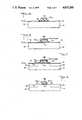
- FIGS. 1 to 9show transverse sectional views of the structure formed at various stages in the fabrication of the LDDFET in accordance with a first embodiment of the invention.
- FIG. 1shows the structure after the initial coating steps wherein the silicon wafer is first coated with a thin, thermally-coated silicon dioxide layer and a n-doped polysilicon layer having on top of it a defined photoresist mask layer with the gate pattern.
- FIG. 2shows the structure after the anisotropic etch of a part of the polysilicon layer.
- FIG. 4shows the structure after the anisotropic etch of the polysilicon layer outside the gate region to expose the source/drain regions.
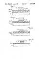
- FIG. 7shows the structure being implanted with a heavy dose of ions.
- the source and drain regions which are formedare illustrated.
- FIG. 8shows the structure after the removal of the silicon dioxide layer.
- FIG. 9shows the structure after lightly doped source/drain regions are formed.
- FIGS. 10-18A second embodiment of the invention is described in FIGS. 10-18.
- FIG. 10shows the structure after the initial coating steps wherein the silicon wafer is first coated with a thin, thermally-coated silicon dioxide layer, a n-doped polysilicon layer, and a silicon nitride layer having on top of it a defined photoresist mask layer with the gate pattern.
- FIG. 12shows the structure after the isotropic etch of part of the photoresist masking layer showing selected portions of the unetched silicon nitride layer exposed.
- FIG. 13shows the structure after the anisotropic etch of the silicon nitride layer and the portion of the polysilicon layer outside the gate region.
- FIG. 14illustrates the structure after the removal of the photoresist masking layer.
- the ladder polysilicon gate with silicon nitride covering the gate regionis shown.
- FIG. 15shows the structure resulting from the oxidation of the outer surface of the polysilicon. The steps are completely oxidized and sidewall polysilicon dioxide spacers are formed.
- FIG. 17shows the structure after the removal of the silicon dioxide and silicon nitride layers.
- FIG. 18shows the structure being doped to form the lightly-doped source/drain regions.
- FIGS. 19 through 23A third embodiment of the invention is shown in FIGS. 19 through 23.
- FIG. 19shows the structure after initial coating steps wherein the silicon wafer is first coated with a thin silicon dioxide layer, an n-doped polysilicon layer, a second thin silicon dioxide layer, and a defined photoresist mask layer with a gate pattern.
- FIG. 20illustrates the structure remaining after the structure shown in FIG. 19 has been anisotropically etched to remove completely the unmasked upper silicon dioxide layer and to remove partially the polysilicon layer.
- FIG. 21shows the structure after the formation of silicon dioxide spacers.
- FIG. 22illustrates the remaining structure after an anisotropic etching step completely removes the unmasked portion of the polysilicon layer.
- FIG. 23illustrates the structure after the removal of the silicon dioxide spacers and the unmasked portion of the first silicon dioxide layer.
- FIGS. 24 through 28A fourth embodiment of the invention is shown in FIGS. 24 through 28.
- FIG. 24shows the structure after initial coating steps wherein the silicon wafer is first coated with a thin silicon dioxide layer, an n-doped polysilicon layer, a silicon nitride layer, and a defined photoresist mask layer with a gate pattern.
- FIG. 25illustrates the structure remaining after the structure shown in FIG. 19 has been anisotropically etched to remove completely the unmasked silicon nitride layer and partially remove the polysilicon layer.
- FIG. 27illustrates the remaining structure after an anisotropic etching step completely removes the unmasked portion of the polysilicon layer.
- FIG. 28illustrates the structure after the removal of the silicon dioxide spacers and the unmasked portion of the silicon dioxide layer.
- LDDFETlightly doped drain field effect transistor
- FIG. 2shows the resulting structure after the unmasked portions of polysilicon 30 are partially etched anisotropically.
- the anisotropic etchingcan be performed using a dry etching process.
- the polysilicon etchis preferably performed by introducing 65 SCCM (standard cubic centimeters per minute) of Ar and 20 SCCM of NF 3 gases into AME-8110 system (trademark of Applied Material Co.) at a pressure of 40 milli-torr and a D.C. bias of -230 V.
- the etch rateis about 250 ⁇ 15 Angstroms/min.
- the amount of the polysilicon layer removedis carefully determined, typically 700 Angstroms.
- the remainder of the unmasked polysilicon layer, designated by the reference character 32,is left on the silicon dioxide.
- FIG. 3shows the resulting structure after the photoresist masking layer is isotropically etched.
- This etch stepexposes the desired portion of the etch-resistant polysilicon 30.
- the isotropic etchingcan be performed using dry etching process, for example, by introducing 50 SCCM of O 2 gas into AME-8110 system, at a pressure of 100 milli-torr and a power of 300 watts to etch the photoresist at a lateral rate of about 800 ⁇ 30 Angstroms/min.
- the remaining portion of photoresist masking layer 40is designated by the reference character 42.
- the remaining portion of the unetched polysilicon 30is designated by the reference character 34.
- FIG. 4shows the structure after a portion of polysilicon layer 32 is removed completely by anisotropic etching using a AME-8110 system.
- a polysilicon “step,” designated by the reference character 36which surrounds the bottom of the polysilicon gate 30, the latter being under the eroded photoresist masking layer 42.
- the polysilicon step 36is the remainder of the exposed unetched polysilicon 34 after the first polysilicon anisotropic etching.
- the length of this stepcorresponds to the length of lightly-doped regions and is in the range of 0.25 -0.30 micrometer for standard applications.
- the thickness of polysilicon step 36is, making reference to FIG.
- the thickness of polysilicon step 36is, in this example, 700 Angstroms.
- FIG. 6illustrates the structure after the polysilicon layer is oxidized.
- the oxidationcompletely oxidizes the thin polysilicon steps 36.
- the thickness of the oxidized step 50is about twice the thickness of the unoxidized material 36.
- the thickness of the oxidemust be sufficient to mask the silicon during the source/drain implantation step. For example, if a 60 kilo-electron-volt (KeV) arsenic dopant implantation is to be used, a 1400 Angstroms silicon dioxide must be formed.
- the polysilicon gate 30is also oxidized during this step and, as can be seen in FIG. 6, the resulting polysilicon gate 38 is thinner.
- This polysilicon oxidation stepmay be performed in the ambient of 5 min. O 2 +45 min. O 2 & HCL+15 min. N 2 at 920° C. in a furnace.
- the silicon dioxide layer 22is thicker due to the oxidation of silicon at source/drain regions. This thickness is controlled so that the projected range of arsenic in silicon dioxide is sufficient to allow the peak of the dose distribution penetrating into the silicon to form source/drain regions. If the thickness of the silicon dioxide 22 is thicker than that of the projected range of arsenic in silicon dioxide, an etch using diluted hydrogen fluoride solution may be used.
- FIG. 7shows the resulting structure after the source/drain region is heavily dosed by an ion implantation process.
- the portions not covered by the polysilicon oxideform the highly-doped source/drain regions 62.
- 6 ⁇ 10 15 doses/cm 2 at 60 KeV energyis used in the source/drain ion implantation process.
- FIG. 8shows the resulting structure after the silicon dioxide layers 22 and 50 are removed. These layers may be removed by etching with a buffered oxide etchant or a diluted hydrogen fluoride solution. The lengths of the regions 52 between the polysilicon gate 38 and source/drain regions 62 are equal, and ready to be formed into the lightly-doped regions.
- FIG. 9shows the resulting LDDFET structure after the lightly-dosed source/drain ion implantation step is performed.
- the conditions of the light dose source/drain ion implantation stepfor example, are 1 ⁇ 10 13 dose/cm 2 , phosphorus at 50 KeV.
- the lightly-doped source/drain regions 64are self-aligned.
- the LDDFETis ready for practical applications.
- the process described abovecan be modified by adding a silicon nitride layer on the polysilicon layer.
- a silicon nitride layerBy applying the anisotropic film etching and the isotropic photoresist etching, a ladder-shaped polysilicon gate covered with silicon nitride can be obtained.
- the silicon nitrideserves as oxidation resisting layer to prevent the oxidation of the top of the gate. This avoids any possible decrease in the thickness of the polysilicon gate.
- FIGS. 10-18The fundamental steps of this embodiment are shown in FIGS. 10-18. Since the specific processing steps are readily understood from the description of FIGS. 1-9 (that is, the first embodiment of the invention), in discussing these figures reference will be made only to the significant modifications.
- a silicon nitride layeris deposited atop the polysilicon layer. This layer may be deposited using conventional low pressure chemical vapor deposition (LPCVD) or plasma-enhanced chemical vapor deposition (PECVD). Thereafter, an anisotropic etching step is performed using reactive-ion etching process to completely remove the unmasked silicon nitride and partially removed the unmasked polysilicon.
- LPCVDlow pressure chemical vapor deposition
- PECVDplasma-enhanced chemical vapor deposition
- the anisotropic etchingcan be performed using the reactive-ion etching system, for example, the AME-8110 system.
- the silicon nitride etchingis performed using 60 SCCM of CHF 3 and 35 SCCM of O 2 at a pressure of 40 milli-torr and a power of 600 watts. This gives an etch rate of about 630 ⁇ 10 Angstroms/min.
- For polysilicon etching65 SCCM of Ar and 20 SCCM of NF 3 , a pressure of 40 milli-torr and a D.C. bias of -230 V are preferred, with the etch rate being about 250 ⁇ 15 Angstroms/min.
- FIG. 12After the mask erosion step, the structure shown in FIG. 12 is formed. This step is comparable to that shown in FIG. 3 of the first embodiment of the invention.
- the structure in FIG. 13is achieved after a second anisotropic etching step under conditions comparable to those discussed above, except here the etching is continued until all of the unmasked polysilicon is removed except for a thin, typically 700 Angstrom, peripheral step of polysilicon surrounding the gate region.
- FIGS. 14 and 15show the structure after the removal of the photoresist and the oxidation of the polysilicon, respectively. It will be recognized that the structure shown in FIG. 15 is comparable to that illustrated in FIG. 6, except that silicon nitride covers the central polysilicon layer rather than polysilicon oxide shown in FIG. 6.
- the further steps in the processinclude the heavy ion implantation step shown in FIG. 16 to form the heavily doped source and drain regions, the removal of the silicon nitride layer and the silicon dioxide shown in FIG. 17, and finally the light ion implantation step shown in FIG. 18, the latter being comparable to that shown in FIG. 9 of the first embodiment.
- FIGS. 19-23 and 24-28Third and fourth embodiments of the invention are shown in FIGS. 19-23 and 24-28. Basically, the steps illustrated serve to form a structure comparable to that formed in FIG. 5 of the first embodiment of the invention.
- the third and fourth embodimentsdiffer fundamentally in that, in the fourth embodiment, as shown in FIG. 24, a silicon nitride layer is placed atop of the polysilicon layer, while in the third embodiment a second silicon dioxide layer 70 is used (FIG. 19).
- the key variation in these embodimentsis the formation of oxide spacers after the anisotropic etching of the unmasked silicon dioxide or silicon nitride layer, as the case may be, and the partial removal of the polysilicon layer shown in FIGS. 20 and 25. This oxide spacer, illustrated in FIGS.
- FIGS. 21 and 26is formed by CVD oxide deposition and anisotropic etching.
- the spaceris designated by the character 82 on FIG. 21.
- the structure shown in FIGS. 21 and 26is subject to anisotropic etching to completely remove the unmasked portion 31 of the polysilicon layer.
- the residual "step" 36remains under the oxide sidewall spacer.
- FIGS. 23 and 28illustrate the structure remaining after an isotropic oxide etching process removes the spacers and the unmasked portion of the silicon dioxide.
- the ladder-shaped polysilicon gates formed, as shown in FIGS. 23 and 28,are thereafter subjected to the polysilicon oxidation, heavy ion implantation step, oxide removal step, and light implantation step described in the first and second embodiments of the invention.
Landscapes
- Insulated Gate Type Field-Effect Transistor (AREA)
Abstract
Description
Claims (15)
Priority Applications (1)
| Application Number | Priority Date | Filing Date | Title |
|---|---|---|---|
| US07/072,086US4837180A (en) | 1987-07-09 | 1987-07-09 | Ladder gate LDDFET |
Applications Claiming Priority (1)
| Application Number | Priority Date | Filing Date | Title |
|---|---|---|---|
| US07/072,086US4837180A (en) | 1987-07-09 | 1987-07-09 | Ladder gate LDDFET |
Publications (1)
| Publication Number | Publication Date |
|---|---|
| US4837180Atrue US4837180A (en) | 1989-06-06 |
Family
ID=22105476
Family Applications (1)
| Application Number | Title | Priority Date | Filing Date |
|---|---|---|---|
| US07/072,086Expired - LifetimeUS4837180A (en) | 1987-07-09 | 1987-07-09 | Ladder gate LDDFET |
Country Status (1)
| Country | Link |
|---|---|
| US (1) | US4837180A (en) |
Cited By (29)
| Publication number | Priority date | Publication date | Assignee | Title |
|---|---|---|---|---|
| US4907048A (en)* | 1987-11-23 | 1990-03-06 | Xerox Corporation | Double implanted LDD transistor self-aligned with gate |
| US4963504A (en)* | 1987-11-23 | 1990-10-16 | Xerox Corporation | Method for fabricating double implanted LDD transistor self-aligned with gate |
| US4968646A (en)* | 1988-12-20 | 1990-11-06 | Thomson Composants Militaires Et Spatiaux | Process for fabricating small size electrodes in an integrated circuit |
| US4978626A (en)* | 1988-09-02 | 1990-12-18 | Motorola, Inc. | LDD transistor process having doping sensitive endpoint etching |
| US5015599A (en)* | 1989-11-03 | 1991-05-14 | U.S. Philips Corporation | Method of manufacturing a device comprising MIS transistors having a projecting gate on the weakly doped parts of source and drain regions |
| US5015598A (en)* | 1989-11-03 | 1991-05-14 | U.S. Philips Corporation | Method of manufacturing a device comprising MIS transistors having a gate electrode in the form of an inverted "T" |
| US5032535A (en)* | 1988-04-26 | 1991-07-16 | Kabushiki Kaisha Toshiba | Method of manufacturing semiconductor device |
| US5102816A (en)* | 1990-03-27 | 1992-04-07 | Sematech, Inc. | Staircase sidewall spacer for improved source/drain architecture |
| US5102815A (en)* | 1990-12-19 | 1992-04-07 | Intel Corporation | Method of fabricating a composite inverse T-gate metal oxide semiconductor device |
| FR2669466A1 (en)* | 1990-11-16 | 1992-05-22 | Haond Michel | METHOD FOR ETCHING INTEGRATED CIRCUIT LAYERS WITH FIXED DEPTH AND CORRESPONDING INTEGRATED CIRCUIT. |
| US5120673A (en)* | 1990-01-25 | 1992-06-09 | Nec Corporation | Process of fabricating field effect transistor with ldd structure |
| US5177571A (en)* | 1988-10-24 | 1993-01-05 | Mitsubishi Denki Kabushiki Kaisha | Ldd mosfet with particularly shaped gate electrode immune to hot electron effect |
| US5228950A (en)* | 1990-12-04 | 1993-07-20 | Applied Materials, Inc. | Dry process for removal of undesirable oxide and/or silicon residues from semiconductor wafer after processing |
| US5238859A (en)* | 1988-04-26 | 1993-08-24 | Kabushiki Kaisha Toshiba | Method of manufacturing semiconductor device |
| US5766991A (en)* | 1990-05-11 | 1998-06-16 | U.S. Philips Corporation | CMOS process utilizing disposable silicon nitride spacers for making lightly doped drain |
| US5837588A (en)* | 1998-01-26 | 1998-11-17 | Texas Instruments-Acer Incorporated | Method for forming a semiconductor device with an inverse-T gate lightly-doped drain structure |
| US5856227A (en)* | 1997-05-01 | 1999-01-05 | Taiwan Semiconductor Manufacturing Company, Ltd. | Method of fabricating a narrow polycide gate structure on an ultra-thin gate insulator layer |
| US6069046A (en)* | 1997-11-26 | 2000-05-30 | Advanced Micro Devices, Inc. | Transistor fabrication employing implantation of dopant into junctions without subjecting sidewall surfaces of a gate conductor to ion bombardment |
| US6110785A (en)* | 1998-04-29 | 2000-08-29 | Advanced Micro Devices, Inc. | Formulation of high performance transistors using gate trim etch process |
| US6110838A (en)* | 1994-04-29 | 2000-08-29 | Texas Instruments Incorporated | Isotropic polysilicon plus nitride stripping |
| US6168993B1 (en)* | 2000-01-19 | 2001-01-02 | Advanced Micro Devices, Inc. | Process for fabricating a semiconductor device having a graded junction |
| US6284612B1 (en)* | 1998-03-25 | 2001-09-04 | Texas Instruments - Acer Incorporated | Process to fabricate ultra-short channel MOSFETs with self-aligned silicide contact |
| US6475842B1 (en)* | 2000-08-09 | 2002-11-05 | Agere Systems Inc. | Process for gate oxide side-wall protection from plasma damage to form highly reliable gate dielectrics |
| US6566178B2 (en)* | 2001-04-30 | 2003-05-20 | Hannstar Display Corporation | Transistor and associated driving device |
| US7041540B1 (en)* | 2005-02-01 | 2006-05-09 | Chunghwa Picture Tubes, Ltd. | Thin film transistor and method for fabricating the same |
| US7256113B1 (en)* | 2001-12-14 | 2007-08-14 | Advanced Micro Devices, Inc. | System for forming a semiconductor device and method thereof |
| US20080188068A1 (en)* | 2007-02-06 | 2008-08-07 | Trivedi Vishal P | Method of forming a semiconductor device having a removable sidewall spacer |
| US20080188067A1 (en)* | 2007-02-06 | 2008-08-07 | Freescale Semiconductor, Inc. | Process of forming an electronic device including forming a gate electrode layer and forming a patterned masking layer |
| WO2015188522A1 (en)* | 2014-06-13 | 2015-12-17 | 京东方科技集团股份有限公司 | Thin film transistor and manufacturing method therefor, and display device |
Citations (5)
| Publication number | Priority date | Publication date | Assignee | Title |
|---|---|---|---|---|
| JPS54161282A (en)* | 1978-06-12 | 1979-12-20 | Toshiba Corp | Manufacture of mos semiconductor device |
| JPS5662367A (en)* | 1979-10-26 | 1981-05-28 | Hitachi Ltd | Manufacturing of semiconductor device |
| JPS57141337A (en)* | 1981-02-24 | 1982-09-01 | Bunshiyoudou:Kk | Turnover device for stacked paper |
| JPS59220971A (en)* | 1983-05-31 | 1984-12-12 | Toshiba Corp | Manufacturing method of semiconductor device |
| JPS6055665A (en)* | 1983-09-06 | 1985-03-30 | Toshiba Corp | Manufacturing method of semiconductor device |
- 1987
- 1987-07-09USUS07/072,086patent/US4837180A/ennot_activeExpired - Lifetime
Patent Citations (5)
| Publication number | Priority date | Publication date | Assignee | Title |
|---|---|---|---|---|
| JPS54161282A (en)* | 1978-06-12 | 1979-12-20 | Toshiba Corp | Manufacture of mos semiconductor device |
| JPS5662367A (en)* | 1979-10-26 | 1981-05-28 | Hitachi Ltd | Manufacturing of semiconductor device |
| JPS57141337A (en)* | 1981-02-24 | 1982-09-01 | Bunshiyoudou:Kk | Turnover device for stacked paper |
| JPS59220971A (en)* | 1983-05-31 | 1984-12-12 | Toshiba Corp | Manufacturing method of semiconductor device |
| JPS6055665A (en)* | 1983-09-06 | 1985-03-30 | Toshiba Corp | Manufacturing method of semiconductor device |
Non-Patent Citations (4)
| Title |
|---|
| Huang et al., "A Novel Submicron LDD Transistor with Inverse-T Gate Structure", IEDM 1986, pp. 742-745. |
| Huang et al., A Novel Submicron LDD Transistor with Inverse T Gate Structure , IEDM 1986, pp. 742 745.* |
| Ohta et al., "A Quadruply Self-Aligned MOA (QSA MOS) a New Short Channel High Speed High Density MOSFET for VLSI", IEDM 1979, pp. 581-584. |
| Ohta et al., A Quadruply Self Aligned MOA (QSA MOS) a New Short Channel High Speed High Density MOSFET for VLSI , IEDM 1979, pp. 581 584.* |
Cited By (36)
| Publication number | Priority date | Publication date | Assignee | Title |
|---|---|---|---|---|
| US4963504A (en)* | 1987-11-23 | 1990-10-16 | Xerox Corporation | Method for fabricating double implanted LDD transistor self-aligned with gate |
| US4907048A (en)* | 1987-11-23 | 1990-03-06 | Xerox Corporation | Double implanted LDD transistor self-aligned with gate |
| US5238859A (en)* | 1988-04-26 | 1993-08-24 | Kabushiki Kaisha Toshiba | Method of manufacturing semiconductor device |
| US5032535A (en)* | 1988-04-26 | 1991-07-16 | Kabushiki Kaisha Toshiba | Method of manufacturing semiconductor device |
| US4978626A (en)* | 1988-09-02 | 1990-12-18 | Motorola, Inc. | LDD transistor process having doping sensitive endpoint etching |
| US5177571A (en)* | 1988-10-24 | 1993-01-05 | Mitsubishi Denki Kabushiki Kaisha | Ldd mosfet with particularly shaped gate electrode immune to hot electron effect |
| US4968646A (en)* | 1988-12-20 | 1990-11-06 | Thomson Composants Militaires Et Spatiaux | Process for fabricating small size electrodes in an integrated circuit |
| US5015599A (en)* | 1989-11-03 | 1991-05-14 | U.S. Philips Corporation | Method of manufacturing a device comprising MIS transistors having a projecting gate on the weakly doped parts of source and drain regions |
| US5015598A (en)* | 1989-11-03 | 1991-05-14 | U.S. Philips Corporation | Method of manufacturing a device comprising MIS transistors having a gate electrode in the form of an inverted "T" |
| US5120673A (en)* | 1990-01-25 | 1992-06-09 | Nec Corporation | Process of fabricating field effect transistor with ldd structure |
| US5102816A (en)* | 1990-03-27 | 1992-04-07 | Sematech, Inc. | Staircase sidewall spacer for improved source/drain architecture |
| US5766991A (en)* | 1990-05-11 | 1998-06-16 | U.S. Philips Corporation | CMOS process utilizing disposable silicon nitride spacers for making lightly doped drain |
| FR2669466A1 (en)* | 1990-11-16 | 1992-05-22 | Haond Michel | METHOD FOR ETCHING INTEGRATED CIRCUIT LAYERS WITH FIXED DEPTH AND CORRESPONDING INTEGRATED CIRCUIT. |
| EP0487380A1 (en)* | 1990-11-16 | 1992-05-27 | France Telecom | Process for etching layers at a given depth in integrated circuits |
| US5330617A (en)* | 1990-11-16 | 1994-07-19 | France Telecom | Method for etching integrated-circuit layers to a fixed depth and corresponding integrated circuit |
| US5228950A (en)* | 1990-12-04 | 1993-07-20 | Applied Materials, Inc. | Dry process for removal of undesirable oxide and/or silicon residues from semiconductor wafer after processing |
| US5102815A (en)* | 1990-12-19 | 1992-04-07 | Intel Corporation | Method of fabricating a composite inverse T-gate metal oxide semiconductor device |
| US6110838A (en)* | 1994-04-29 | 2000-08-29 | Texas Instruments Incorporated | Isotropic polysilicon plus nitride stripping |
| US5856227A (en)* | 1997-05-01 | 1999-01-05 | Taiwan Semiconductor Manufacturing Company, Ltd. | Method of fabricating a narrow polycide gate structure on an ultra-thin gate insulator layer |
| US6069046A (en)* | 1997-11-26 | 2000-05-30 | Advanced Micro Devices, Inc. | Transistor fabrication employing implantation of dopant into junctions without subjecting sidewall surfaces of a gate conductor to ion bombardment |
| US5837588A (en)* | 1998-01-26 | 1998-11-17 | Texas Instruments-Acer Incorporated | Method for forming a semiconductor device with an inverse-T gate lightly-doped drain structure |
| US6284612B1 (en)* | 1998-03-25 | 2001-09-04 | Texas Instruments - Acer Incorporated | Process to fabricate ultra-short channel MOSFETs with self-aligned silicide contact |
| US6110785A (en)* | 1998-04-29 | 2000-08-29 | Advanced Micro Devices, Inc. | Formulation of high performance transistors using gate trim etch process |
| US6168993B1 (en)* | 2000-01-19 | 2001-01-02 | Advanced Micro Devices, Inc. | Process for fabricating a semiconductor device having a graded junction |
| US6475842B1 (en)* | 2000-08-09 | 2002-11-05 | Agere Systems Inc. | Process for gate oxide side-wall protection from plasma damage to form highly reliable gate dielectrics |
| US6734034B2 (en)* | 2001-04-30 | 2004-05-11 | Hannstar Display Corporation | Transistor and associated driving device |
| US20030194838A1 (en)* | 2001-04-30 | 2003-10-16 | Po-Sheng Shih | Transistor and associated driving device |
| US6566178B2 (en)* | 2001-04-30 | 2003-05-20 | Hannstar Display Corporation | Transistor and associated driving device |
| US7256113B1 (en)* | 2001-12-14 | 2007-08-14 | Advanced Micro Devices, Inc. | System for forming a semiconductor device and method thereof |
| US7041540B1 (en)* | 2005-02-01 | 2006-05-09 | Chunghwa Picture Tubes, Ltd. | Thin film transistor and method for fabricating the same |
| US20080188068A1 (en)* | 2007-02-06 | 2008-08-07 | Trivedi Vishal P | Method of forming a semiconductor device having a removable sidewall spacer |
| US20080188067A1 (en)* | 2007-02-06 | 2008-08-07 | Freescale Semiconductor, Inc. | Process of forming an electronic device including forming a gate electrode layer and forming a patterned masking layer |
| US7727829B2 (en)* | 2007-02-06 | 2010-06-01 | Freescale Semiconductor, Inc. | Method of forming a semiconductor device having a removable sidewall spacer |
| US7737018B2 (en) | 2007-02-06 | 2010-06-15 | Freescale Semiconductor, Inc. | Process of forming an electronic device including forming a gate electrode layer and forming a patterned masking layer |
| WO2015188522A1 (en)* | 2014-06-13 | 2015-12-17 | 京东方科技集团股份有限公司 | Thin film transistor and manufacturing method therefor, and display device |
| US9748398B2 (en)* | 2014-06-13 | 2017-08-29 | Boe Technology Group Co., Ltd. | Thin film transistor and manufacturing method thereof, display device |
Similar Documents
| Publication | Publication Date | Title |
|---|---|---|
| US4837180A (en) | Ladder gate LDDFET | |
| US4906589A (en) | Inverse-T LDDFET with self-aligned silicide | |
| US4818715A (en) | Method of fabricating a LDDFET with self-aligned silicide | |
| US5818085A (en) | Body contact for a MOSFET device fabricated in an SOI layer | |
| USH986H (en) | Field effect-transistor with asymmetrical structure | |
| JP3029653B2 (en) | Method for manufacturing semiconductor device | |
| US6127699A (en) | Method for fabricating MOSFET having increased effective gate length | |
| US5656518A (en) | Method for fabrication of a non-symmetrical transistor | |
| US5714393A (en) | Diode-connected semiconductor device and method of manufacture | |
| US6184155B1 (en) | Method for forming a ultra-thin gate insulator layer | |
| JP2586342B2 (en) | Method for manufacturing semiconductor device | |
| US5705439A (en) | Method to make an asymmetrical LDD structure for deep sub-micron MOSFETS | |
| US5654215A (en) | Method for fabrication of a non-symmetrical transistor | |
| US5427971A (en) | Method for fabrication of semiconductor elements | |
| US5923982A (en) | Method of making asymmetrical transistor with lightly and heavily doped drain regions and ultra-heavily doped source region using two source/drain implant steps | |
| US5858847A (en) | Method for a lightly doped drain structure | |
| EP0439173A2 (en) | Process of fabricating field effect transistor with LDD structure | |
| US6906345B2 (en) | Semiconductor device and method of manufacturing the same | |
| US5915181A (en) | Method for forming a deep submicron MOSFET device using a silicidation process | |
| US5604138A (en) | Process for making a semiconductor MOS transistor | |
| US6110790A (en) | Method for making a MOSFET with self-aligned source and drain contacts including forming an oxide liner on the gate, forming nitride spacers on the liner, etching the liner, and forming contacts in the gaps | |
| JPH05267331A (en) | Manufacture of mos semiconductor device | |
| US6087238A (en) | Semiconductor device having reduced-width polysilicon gate and non-oxidizing barrier layer and method of manufacture thereof | |
| JPH0831602B2 (en) | Method for manufacturing MIS field effect transistor | |
| KR0170436B1 (en) | Method of manufacturing mosfet |
Legal Events
| Date | Code | Title | Description |
|---|---|---|---|
| AS | Assignment | Owner name:INDUSTRIAL TECHNOLOGY RESEARCH INSTITUTE, CHU-TUNG Free format text:ASSIGNMENT OF ASSIGNORS INTEREST.;ASSIGNOR:CHAO, FUNG-CHING;REEL/FRAME:004786/0875 Effective date:19870820 Owner name:INDUSTRIAL TECHNOLOGY RESEARCH INSTITUTE, CHU-TUNG Free format text:ASSIGNMENT OF ASSIGNORS INTEREST;ASSIGNOR:CHAO, FUNG-CHING;REEL/FRAME:004786/0875 Effective date:19870820 | |
| STCF | Information on status: patent grant | Free format text:PATENTED CASE | |
| FEPP | Fee payment procedure | Free format text:PAYOR NUMBER ASSIGNED (ORIGINAL EVENT CODE: ASPN); ENTITY STATUS OF PATENT OWNER: LARGE ENTITY | |
| FPAY | Fee payment | Year of fee payment:4 | |
| FEPP | Fee payment procedure | Free format text:PAT HLDR NO LONGER CLAIMS SMALL ENT STAT AS NONPROFIT ORG (ORIGINAL EVENT CODE: LSM3); ENTITY STATUS OF PATENT OWNER: LARGE ENTITY Free format text:PAYER NUMBER DE-ASSIGNED (ORIGINAL EVENT CODE: RMPN); ENTITY STATUS OF PATENT OWNER: LARGE ENTITY | |
| FPAY | Fee payment | Year of fee payment:8 | |
| FEPP | Fee payment procedure | Free format text:PAYOR NUMBER ASSIGNED (ORIGINAL EVENT CODE: ASPN); ENTITY STATUS OF PATENT OWNER: LARGE ENTITY | |
| FPAY | Fee payment | Year of fee payment:12 |