US4831456A - Imaging apparatus using a solid-state imaging element having a substrate - Google Patents
Imaging apparatus using a solid-state imaging element having a substrateDownload PDFInfo
- Publication number
- US4831456A US4831456AUS07/113,824US11382487AUS4831456AUS 4831456 AUS4831456 AUS 4831456AUS 11382487 AUS11382487 AUS 11382487AUS 4831456 AUS4831456 AUS 4831456A
- Authority
- US
- United States
- Prior art keywords
- circuit board
- terminal group
- camera head
- end portion
- external terminal
- Prior art date
- Legal status (The legal status is an assumption and is not a legal conclusion. Google has not performed a legal analysis and makes no representation as to the accuracy of the status listed.)
- Expired - Lifetime
Links
Images


Classifications
- A—HUMAN NECESSITIES
- A61—MEDICAL OR VETERINARY SCIENCE; HYGIENE
- A61B—DIAGNOSIS; SURGERY; IDENTIFICATION
- A61B1/00—Instruments for performing medical examinations of the interior of cavities or tubes of the body by visual or photographical inspection, e.g. endoscopes; Illuminating arrangements therefor
- A61B1/04—Instruments for performing medical examinations of the interior of cavities or tubes of the body by visual or photographical inspection, e.g. endoscopes; Illuminating arrangements therefor combined with photographic or television appliances
- A61B1/05—Instruments for performing medical examinations of the interior of cavities or tubes of the body by visual or photographical inspection, e.g. endoscopes; Illuminating arrangements therefor combined with photographic or television appliances characterised by the image sensor, e.g. camera, being in the distal end portion
- A61B1/051—Details of CCD assembly
- A—HUMAN NECESSITIES
- A61—MEDICAL OR VETERINARY SCIENCE; HYGIENE
- A61B—DIAGNOSIS; SURGERY; IDENTIFICATION
- A61B1/00—Instruments for performing medical examinations of the interior of cavities or tubes of the body by visual or photographical inspection, e.g. endoscopes; Illuminating arrangements therefor
- A61B1/04—Instruments for performing medical examinations of the interior of cavities or tubes of the body by visual or photographical inspection, e.g. endoscopes; Illuminating arrangements therefor combined with photographic or television appliances
- A61B1/05—Instruments for performing medical examinations of the interior of cavities or tubes of the body by visual or photographical inspection, e.g. endoscopes; Illuminating arrangements therefor combined with photographic or television appliances characterised by the image sensor, e.g. camera, being in the distal end portion
- H—ELECTRICITY
- H04—ELECTRIC COMMUNICATION TECHNIQUE
- H04N—PICTORIAL COMMUNICATION, e.g. TELEVISION
- H04N23/00—Cameras or camera modules comprising electronic image sensors; Control thereof
- H04N23/50—Constructional details
- H04N23/54—Mounting of pick-up tubes, electronic image sensors, deviation or focusing coils
- H—ELECTRICITY
- H04—ELECTRIC COMMUNICATION TECHNIQUE
- H04N—PICTORIAL COMMUNICATION, e.g. TELEVISION
- H04N23/00—Cameras or camera modules comprising electronic image sensors; Control thereof
- H04N23/50—Constructional details
- H04N23/555—Constructional details for picking-up images in sites, inaccessible due to their dimensions or hazardous conditions, e.g. endoscopes or borescopes
- H—ELECTRICITY
- H04—ELECTRIC COMMUNICATION TECHNIQUE
- H04N—PICTORIAL COMMUNICATION, e.g. TELEVISION
- H04N23/00—Cameras or camera modules comprising electronic image sensors; Control thereof
- H04N23/60—Control of cameras or camera modules
- H04N23/66—Remote control of cameras or camera parts, e.g. by remote control devices
Definitions
- the present inventionrelates to an imaging apparatus such as an endoscope or a monitor TV camera which comprises a solid-state imaging device in a camera head.
- An endoscopea so-called electronic scope, is known as a conventional imaging apparatus.
- a solid-state imaging deviceSID
- an optical image received by the light-receiving surface of the SIDcan be monitored through a camera control unit.
- An endoscopecomprising a camera head incorporating such an SID is disclosed in Japanese Patent Disclosure No. 60-208726.
- an SID chipis arranged to be perpendicular to the axis of an endoscope insertion section, and external terminals are randomly arranged on the rear surface of the SID. All the external terminals are connected to circuit boards mounting electrical parts. Conductive wire groups of a power cable connecting a camera control unit and the camera head, are connected to all the circuit boards mounting the electrical parts, and are also connected to the external terminals of the SID.
- the imaging apparatus of the present inventioncomprises a camera head and a camera control unit.
- An objective optical systemis arranged at the front end portion of the camera head, and a solid-state imaging device including a first external terminal group of terminals to or from which signals processed inside the camera head are input or output, and a second external terminal group, which is separated from the first external terminal group, and including terminals to or from which signals that are not processed inside the camera head are input or output, is arranged behind the objective optical system.
- One connecting terminal group of a circuit boardwhich has at least two connecting terminal groups is connected to the first external terminal group.
- the other connecting terminal group of the circuit boardis connected to one end portion of a first conductive wire group of a power cable.
- One end portion of a second conductive wire group of the power cableis connected to the second external terminal group.
- the other end portion of each of the first and second conductive wire groupsis connected to the camera control unit.
- the circuit boardis coupled to only the external terminals of the first group, not to all external terminals. It can therefore be relatively small. Further, since no signal exchange is required between the two separated groups of external terminals, the wiring inside the electrical signal processing section is simple and requires but a small space.
- the power cablesare divided into two groups.
- the layout of these cablesis therefore simple, and does not require dead space.
- circuit boardOn the circuit board, there are mounted electronic parts, such as ICs, capacitors, resistors, and transistors, used to amplify the video signals output from the SID, stabilize the voltage applied to the SID, prevents the reflection of signals due to the matching between the camera head and the power cables, and remove noise from the signals.
- electronic partssuch as ICs, capacitors, resistors, and transistors, used to amplify the video signals output from the SID, stabilize the voltage applied to the SID, prevents the reflection of signals due to the matching between the camera head and the power cables, and remove noise from the signals.
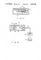
- FIG. 1is a longitudinal sectional view showing an endoscope comprising an imaging apparatus according to a first embodiment of the present invention
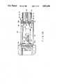
- FIGS. 2 and 3are longitudinal sectional views showing a camera head section of the imaging apparatus illustrated in FIG. 1;
- FIG. 4is a cross-sectional view taken along a line A--A in FIG. 3;
- FIGS. 5 to 7are respectively a front view, a longitudinal sectional view, and a rear view showing a solid-state imaging device according to the first embodiment
- FIGS. 8 and 9are longitudinal sectional views showing a first modification of the camera head section of the imaging apparatus according to the first embodiment
- FIG. 10is a longitudinal sectional view showing a second modification of the camera head section of the imaging apparatus according to the first embodiment
- FIG. 11is a longitudinal sectional view showing a third modification of the camera head section of the imaging apparatus according to the first embodiment
- FIG. 12is a longitudinal sectional view schematically showing a imaging apparatus according to a second embodiment of the present invention.
- FIG. 13is a longitudinal sectional view showing a camera head section of the imaging apparatus according the second embodiment
- FIG. 14is a view showing a wiring state in the camera head
- FIGS. 15 to 17are respectively a plan view, a side view, and a bottom view of a circuit board
- FIGS. 18 to 20are respectively a front view, a longitudinal sectional view, and a bottom view showing a first modification of the solid-state imaging device
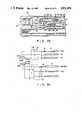
- FIG. 21is a schematic view showing the solid-state imaging device and an electrical circuit shown in FIGS. 18 to 20;
- FIGS. 22 to 24are respectively a front view, a longitudinal sectional view, and a bottom view showing a second modification of the solid-state imaging device
- FIG. 25is a longitudinal sectional view showing a camera head incorporating the solid-state imaging device illustrated in FIGS. 22 to 24;
- FIG. 26is a longitudinal sectional view showing another modification of the camera head section of the imaging apparatus according to the second embodiment
- FIGS. 27 and 28are respectively a longitudinal sectional view and a rear view, showing the solid-state imaging device illustrated in FIG. 26;
- FIG. 29is a longitudinal sectional view showing an imaging apparatus according to a third embodiment of the present invention.
- FIG. 30is a schematic view showing a solid-state imaging device and electrical circuit according to another modification.
- FIG. 1shows the structure of a distal end portion of an insertion section of an endoscope or an electronic scope comprising an imaging apparatus according to the present invention.
- the insertion section of the endoscopecomprises bending section 2.
- a plurality of tubular segments 4 which are rotatably coupled to each otherare arranged in bending section 2.
- the outer surface of each tubular segment 4is covered by braid 6 and rubber sheath 8.
- Metal distal end member 10is coupled to tubular segment 4 arranged in the distal end portion via insulating member 12.
- An exposed portion of distal end member 10is covered with insulating cover 14 and sheath 8.
- Distal end member 10 and sheath 8are connected by threaded adhesive layer 16.
- a plurality of mounting holesar formed in distal end member 10 and insulating cover 14 arranged at the distal end of the insertion section.
- Objective optical system 18 and illumination optical system 20are fitted in the mounting holes.
- Forceps channel 22is constituted by pipe-like insulating member 23 fitted in the mounting hole of distal end member 10, forceps channel pipe 24 engaged with the rear opening portion of the inner hole of insulating member 23, and forceps channel tube 26 coupled to the rear end portion of pipe 24 and extending inside the insertion section.
- Illumination optical system 20 having a plurality of optical lenses 20Aare optically connected to the distal end surface of light guide fiber 28 inserted through the insertion section.
- Solid-state imaging device (SID) 30constituting camera head section 29 of the imaging apparatus, and electrical signal processing section 32 connected to SID 30 are arranged behind objective optical system 18 having a plurality of objective lenses 18A. Therefore, living tissues in a body cavity are observed using SID 30, and diseased tissues can be simultaneously treated using forceps inserted in channel 22.
- SID 30is illustrated in detail in FIGS. 5 to 7.
- SID chip 36, color filter array 37, and cover glass 38are sequentially stacked on base 34 formed of a ceramic multi-layered substrate, and are packaged by seal member 42.
- SID chip 36comprises image area 39, optical black 40, and horizontal shift register 41, and is die-bonded to the surface of base 34.
- Chip electrodes 44 of SID chip 36 and bonding pads 46 with through holes formed on base 34are connected through bonding wires 48. Bonding pads 46 are connected to flat leads consisting of first and second external terminal groups 50A, 50B formed on the bottom surface of base 34.
- Color filter array 37 and cover glass 38are sequentially stacked on the upper surface of SID chip 36, and these components are packaged by seal member 42.
- SID 30 with the above structureis arranged to be perpendicular to the axis of the insertion section of the endoscope, i.e., perpendicular to the optical axis of objective optical system 18 in recess 10A formed in the rear end portion of distal end member 10.
- SID 30is fixed by adhesive layer 52 so that its light receiving surface faces objective optical system 18.
- Electrical signal processing section 32comprises first circuit board 54 on the upper and lower surfaces of which electrical parts are mounted, and second circuit board 56 on which only a conductive pattern is formed. More specifically, IC 58 is arranged on the upper surface of first circuit board 54, and capacitors 60 are mounted on the lower surface. In particular, IC 58 employs a compact package structure, as shown in FIG. 2. More specifically, bare chip 59 is directly die-bonded to first circuit board 54. Bare chip 59 and circuit board 54 are connected through bonding wires 62. A portion around bare chip 59 is sealed by IC seal member 64.
- a large number of L-shaped board lead legs 66are bonded on the upper surface of one edge portion of first circuit board 54, and a large number of grooves 68A are formed on the lower surface of the other edge portion of board 54.
- Shield wire connecting land 68is provided to each groove.
- Bare chip 59 and capacitors 60are connected to some of lead legs 66 and some of shield wire connecting leads 68.
- a large number of L-shaped board lead legs 70are formed on one end portion of second circuit board 56, and pipe-shaped terminals 72 through which lead wires are inserted are formed on the other end portion thereof.
- a wiring patternis formed on the entire surface of board 56, and is connected to lead legs 70 and pipe-shaped terminals 72. An open end portion of each terminals 72 is obliquely cut so that a lead wire can be easily inserted therein.
- first and second circuit boards 54 and 56are less broad than SID 30.
- First and second circuit boards 54 and 56extend to be vertically shifted and parallel to each other.
- Lead legs 66 and 70 of boards 54 and 56are soldered to flat leads 50.
- Boards 54 and 56are arranged along the axial direction of the insertion section.
- Power cable 73 inserted through the insertion sectionis divided into first bundle 74 of shield wires and second bundle 76 of shield wires.
- Each shield wireis soldered to corresponding lead 68 or terminal 72.
- the shield wiresare divided into two bundles 74 and 76 of shield wires, and bundles 74 and 76 are inserted in through holes of shield wire holder 78. Then, shield wire inner conductors 80 and 81 covered with insulating tubes are exposed from the bundles of shield wires.
- conductor 80A of each shield wire inner conductor 80 in first bundle 74 of shield wiresis soldered to lead 68, and conductor 81A of each shield wire inner conductor 81 in second bundle 76 of lead wires is inserted through corresponding pipe-shaped terminal 72 and is soldered thereto.
- Outer conductors 82 of bundles 74 and 76 of shield wiresare bonded to shield wire holder 78 by solder layer 84.
- Holder 78is bonded inside the proximal end portion of metal shield cover 86 arranged to surround circuit boards 54 and 56 by conductive adhesive layer 78A.
- Holder 78is electrically connected to shield cover 86.
- a distal end portion of shield cover 86is electrically connected to metal distal end member 10. Therefore, the entire electrical signal processing section 32 can be shielded.
- First and second bundles of lead wires 74 and 76are adhered to holder 78 by adhesive 88, thereby reinforcing contacting portions.
- circuit boards 54 and 56are arranged along the axial direction of the insertion section. Therefore, if the number of shield wires or electrical components is increased, boards 54 and 56 need only be extended in the axial direction of the insertion section. Therefore, processing section 32 will not become larger than the radial size of the package of SID 30. For this reason, the layout of components such as light guide fiber 28, forceps channel tube 26, and the like is not interfered by the circuit boards connected to the SID, and an insertion section with a thin distal end portion can be formed. Since soldered portions are concentrated on specific portions of circuit boards 54 and 56, a wiring operation can be facilitated.
- the imaging apparatushas the following advantages. More specifically, since lead legs 66 and 70 are provided to the edge portions of boards 54 and 56, manufacture of parts can be facilitated as compared to a case wherein lead legs 66 and 70 are arranged on the rear surface of SID 30. Since metal shield cover 86 is used as a support member for power cable 73, power cable 73 can be reliably supported. Since conductors 80 can be connected only by inserting them into pipe-shaped terminals 72, the wiring operation of the shield wires can be facilitated. Since the shield wires are divided into two bundles, the layout of the cable inside the insertion section of the endoscope can be easily performed.
- the diameter of the insertion sectioncan be decreased, and the resistance of the cable when the bent section is repetitively bent can be improved.
- the circuit boardcan be rendered compact, and hence, the entire electrical signal processing section 32 can also be rendered compact.
- Processing section 32can be perfectly shielded by distal end member 10, shield cover 86, shield wire holder 78, and outer conductors 82, and is satisfactorily protected from noise. Since the shield members are insulated from external metal members at the distal end portion such as tubular segment 4, braid 6, channel pipe 24, and the like, electrical safety can be ensured.
- a first modification of a camera head sectionwill be described with reference to FIGS. 8 and 9.
- the connecting structure and the shield structure of circuit boards 54 and 56are different from those of the first embodiment. More specifically, a plurality of lead legs 92 in two horizontal lines project from the bottom surface of SID 30 which are vertically shifted from each other.
- First and second circuit boards 54 and 56each having flat lands 94 at two edge portions are integrally bonded to each other by substrate integrating member 96. One end portion of the integrated circuit board is inserted between upper and lower lead legs 9 and is soldered thereto.
- circuit boards 54 and 56can be easily aligned to SID 30. Since boards 54 and 56 are integrally bonded to each other, they can be easily fixed to SID 30, thus improving workability.
- Projection 102projects from the rear end portion of distal end member 10.
- L-shaped support member 98 having a shield wire holding portionis mounted on projection 102.
- Member 98is formed of a metal, and is electrically connected to member 10. The upper and two side surfaces of support member 98 are covered with conductive film 100, and insulating filler 104 for holding conductive film 100 is provided inside film 100.
- processing section 32since the entire processing section 32 is not shielded by a hard member unlike in the first embodiment, a space necessary for shielding can be reduced. As a result, processing section 32 can be rendered compact.
- FIGS. 10 and 11show another modification of the camera head section.
- the electrical signal processing section of the camera head section according to the first embodiment of the present inventionis applied to a side-view type endoscope.
- SID 30is incorporated in the front portion of distal end member 10.
- the light receiving surface of SID 30is arranged to face the front surface of objective optical system 18 arranged therebehind.
- First circuit board 54 mounting electrical parts and second circuit board 56 on which only a wiring pattern is formedare arranged to be parallel to each other along the axial direction of the insertion section of the endoscope.
- SID 30 and processing section 32may be arranged behind objective optical system 18.
- FIGS. 12 to 17A second embodiment of an imaging apparatus according to the present invention will now be described with reference to FIGS. 12 to 17.
- electrical signal processing section 32 in camera head 29comprises only first circuit board 54 on which electrical parts are mounted.
- IC 58 and capacitors 60are mounted on the upper surface of board 54.
- Power cable 73 connected to camera head 29is connected to camera control unit (CCU) 105.
- CCU 105is connected to TV monitor 107.
- IC 58employs a compact package structure. Bare chip 59 is bonded onto first circuit board 54. Chip 59 and board 54 are connected through bonding wires 62. A portion around chip 59 is sealed by IC seal member 64.
- Power cable 73is divided, over the overall length of the power cable, into first bundle 74 of shield wires including signal lines subjected to signal processing inside the camera head, and second bundle 76 of shield wires consisting of signal lines which are not subjected to signal processing, and the bundles are respectively inserted in two through holes of cable holder 78.
- Shield wire inner conductors 81 of bundle 76are directly connected to terminals 50h to 50n (shown in FIG. 7) which are not subjected to signal processing inside processing section 32, i.e., the camera head.
- Shield wire inner conductors 80 of bundle 74are connected to terminals formed on the rear end portion of first circuit board 54.
- a reset pulse terminal ( ⁇ R) of SID chip 36is connected to ( ⁇ R) of shield wire 111 through chip electrode 44a, bonding pad 46, and flat lead 50n.
- a power supply terminal (VDD) of SID chip 36is connected to (VDD) of simple wire 112 through chip electrode 44b, bonding pad 46b, flat lead 50e, and first circuit board 54.
- a video output terminal (Vout)is connected to a shield wire (Vout) through chip electrode 44c, bonding pad 46c, flat lead 50c, and first circuit board 54.
- a load gate terminal(LG) (a constant current source for an output buffer, i.e., an applied voltage line for setting a current value upon transfer) is connected to first circuit board 54 through chip electrode 44d, bonding pad 46d, and flat lead 50b.
- An output gate terminal(OG) (an output line for an output buffer) is connected to first circuit board 54 through chip electrode 44e, bonding pad 46e, and flat lead 50b.
- terminals (H1, H2) for horizontal clock pulses (1) and (2) as a CCD transfer groupthe terminal for the horizontal clock pulse (1) is connected to a shield wire (H1) through chip electrode 44f, bonding pad 46f, and flat lead 50m, and the terminal for the horizontal clock pulse (2) is connected to a shield wire (H2) through chip electrode 44g, bonding pad 46g, and flat lead 50l.
- a test terminal (IG) which is used for testing a CCD before it is incorporated in the camera head and is used as a GND terminal after testingis connected to first circuit board 54 through chip electrode 44f, bonding pad 46h, and flat lead 50f.
- terminals (V1, V2, V3, V4) for vertical clock pulses (1), (2), (3), and (4) as a CCD transfer groupthe terminal for the vertical clock pulse (1) is connected to a shield wire (V1) through chip electrode 44i, bonding pad 46i, and flat lead 50k.
- the terminal for the vertical clock pulse (2)is connected to a shield wire (V2) through chip electrode 44j, bonding pad 46j, and flat lead 50i.
- the terminal for the clock pulse (3)is connected to a shield wire (V3) through chip electrode 44k, bonding pad 46k, and flat lead 50j.
- the terminal for the vertical clock pulse (4)is connected to a shield wired (V4) through chip electrode 44l, bonding pad 46l, and flat lead 50h.
- a terminal (PW) connected to an electrode of an intermediate layer of a CCD waferis connected to first circuit board 54 through chip electrode 44m, bonding pad 46m, and flat lead 50g.
- a substrate power supply terminal (Vsub) connected to an electrode of a lowermost layer of the CCD waferis connected to first circuit board 54 through chip electrode 44n, bonding pad 46n, and flat lead 50a.
- Flat leads 50h to 50n to which terminals ⁇ R, H1, H2, V1, V2, V3, and V4 of SID chip 36 are connected,are terminals which receive signals that need not be processed inside the camera head. These leads are arranged in line on one side of base 14, and are directly connected to the inner conductors of shield wires.
- Flat leads 50a to 50g connected to terminals VDD, Vout, LG, OG, IG, PW, and Vsub of chip 36are terminals to or from which signals that must be processed inside the camera head are input or output. These leads are connected to the terminals of circuit board 54.
- Selection terminals 118A and 118B of circuit board 54 shown in FIG. 14are used for adjusting variations in drive voltages (OG) and (Vsub) during manufacture of the SID, and connections between terminals are selected in accordance with characteristics of individual SIDs.
- the IG terminal (50f) and the PW terminal (50g) of SID chip 36are used for testing the electrical performance of the SID chip itself. In a mounting state after the test, these terminals are electrically connected to each other on circuit board 54.
- a dummy cable connected to circuit board 54is used for removing noise components of the Vout cable. More specifically, noise components of the Vout cable can be removed by utilizing the fact that the noise components appearing on the dummy cable are the same as those on the Vout cable.
- FIGS. 15, 16, and 17illustrate circuit board 54 in detail.
- circuit board 54has patterns 106 connected to flat leads 50a to 50g on the left side portion, and each pattern 106 has through hole 108 for arranging and wiring an electrical part on circuit board 54.
- side-surface through holes 110are formed on the side surface of circuit board 54.
- a molded elementis not used as IC 58, and bare chip (IC chip) 59 is attached onto circuit board 54 and is connected to the patterns on circuit board 54 by bonding wires 62.
- IC chip 59 and the connecting portionsare sealed by IC seal member 64 in order to protect them from an outer atmosphere.
- Patterns 114 for connecting inner conductors 80 of shield wires 111 and simple wires 112are provided on the right side portion of circuit board 54.
- first bundle of shield wires 74consists of two coaxial shield wires 111 (Vout and dummy wires), and two simple wires 112 (GND and VDD wires). Inner conductor 80 of each shield wire 111 and each simple wire 112 are connected to patterns 114 of circuit board 54. Outer conductors 92 of shield wires 74 are electrically connected to cable holder 78.
- Second bundle of shield wires 76consists of seven coaxial shield wires 111 (V1, V2, V3, V4, H1, H2, and ⁇ R), and inner conductors 81 of shield wires 111 are directly connected to flat leads 50h to 50n of the SID, and outer conductors 82 are electrically connected to cable holder 78.
- Bundles 74 and 76 of shield wiresare covered by unit shield 116, and the proximal end portion of shield 116 is connected to a ground terminal (not shown) of the CCU. Shield 116 is further covered by cable protection sheath 118.
- the wiring inside the electrical signal processing sectionis simplified, and the layout of the components requires a minimum space.
- the processing sectioncan be rendered compact, and the entire camera head can be made compact.
- No second circuit board having a wiring patternis mounted on the terminal group of the SID for receiving signals which are not subjected to signal processing in the camera head, and the cable is directly connected to the terminal group.
- a soldered portioncan be eliminated, and workability can be improved.
- the imaging apparatus according to the second embodimentemploys a simultaneous type SID.
- An imaging apparatus according to this modificationemploys a frame-sequential type SID.
- Frame-sequential type SID 30comprises base 34.
- SID chip 36is die-bonded onto the upper surface of base 34.
- SID chip 36has chip electrodes 120a to 120f, image area 39, optical black 40, and horizontal shift register 41. Bonding pads 122a to 122f with through holes are provided on two edge portions of the upper surface of base 34.
- Chip electrodes 120a to 120f and bonding pads 122a to 122fare connected through bonding wires 48.
- Pin-shaped leads 124a, to 124felectrically connected to bonding pads 122a to 122f project from the bottom surface of base 34.
- a parallel clock pulse terminal ( ⁇ P) of SID chip 36is connected to ( ⁇ P) of shield wire 111 through chip electrode 120a, bonding pad 122a, and lead 124c.
- a serial clock pulse terminal ( ⁇ S)is connected to a shield wire ( ⁇ S) through chip electrode 120b, bonding pad 122b, and lead 124b.
- An anti-blooming gate terminal( ⁇ AB) is connected to a shield wire ( ⁇ AB) through chip electrode 120c, bonding pad 122c, and lead 124a.
- a substrate terminal (Vsub)is connected to first circuit board 54 via chip electrode 120d, bonding pad 122d, and lead 124f.
- a video output terminal (Vout)is connected to a shield wire (Vout) through chip electrode 120e, bonding pad 122e, lead 124e, and first circuit board 54.
- a power supply terminal(VDD) is connected to a simple wire (VDD) through chip electrode 120f, bonding pad 122f, lead 124d, and first circuit board 54.
- Leads 124a, 124b, and 124c connected to terminals ⁇ P, ⁇ S, and ⁇ AB which are not subjected signal processing in the processing sectionare aligned in line on one side of the rear surface of base 34.
- Leads 124d, 124e, and 124f connected to terminals Vsub, Vout, and VDD which are subjected signal processing in the processing sectionare aligned in line on the opposite side on the rear surface of base 34.
- Leads 124a, 124b, and 124eare connected to the shield wires ( ⁇ AB, ⁇ S, and ( ⁇ P), respectively, and leads 124d, 124e, and 124f are connected to the terminals of circuit board 54.
- Power cable 73consists of two simple wires 112 (VDD and GND), and five shield wires 111 ( ⁇ AB, ⁇ S, ⁇ P, Vout, and dummy), and is covered with unit shield 116.
- VDD and GNDsimple wires 112
- ⁇ AB, ⁇ S, ⁇ P, Vout, and dummyshield wires 111
- unit shield 116Other arrangements in this modification are the same as those in the second embodiment, and a detailed description thereof will be omitted.
- SID 30external I/O terminals 124a to 124f are arranged on the side surface of SID chip 36.
- the external terminalsare divided into a first terminal group which are subjected to signal processing inside electrical signal processing section 32, and a second terminal group which is not subjected to signal processing inside processing section 32, and the terminal groups are separately arranged.
- SID chip 36 and external I/O terminals 124a to 124fare connected by bumps 128, and the respective terminals are separated in the same manner as in SID 30 according to the first modification.
- the pattern on circuit board 54is based on the circuit diagram shown in FIG. 21.
- a pattern for connecting terminals 124d, 124e, and 124f of SID 30 subjected signal processing inside processing section 32 to inner conductors 81 of shield wires 111 and simple wires 122is provided on one surface of circuit board 54, and a pattern for mounting IC 58 and capacitor 60 is provided on the other surface of circuit board 54.
- Cable 73is divided into a cable group consisting of only signal lines which are not subjected to signal processing inside the camera head, and another cable group subjected to signal processing therein, immediately before cable holder 78.
- Inner conductors 80 of the cable group consisting of signal lines which are not subjected to signal processingfurther extend from cable holder 78, and are directly connected to terminals 124d, 124e, and 124f of the SID which are not subjected signal processing in the camera head.
- Outer conductors 82 of shield wires 111are soldered to cable holder 78.
- FIGS. 26 to 28show a third modification.
- power cable 73is not divided along the entire length of the cable but is divided into two groups immediately before electrical signal processing section 32.
- External terminal groups on one side of SID 30are aligned in line in the previous embodiments and modifications.
- a terminal group on one sideis arranged in line and the other terminal group is arranged in two lines.
- Each of two terminal groups of SID 30may be aligned in two or more lines.
- external terminalsare separated into a first external terminal group connected to a surrounding circuit inside a camera head, and a second external terminal group which are not connected thereto.
- a circuit board for a peripheral circuitcan be designed to be compact, and the wiring inside the electrical signal processing section can be simplified. Therefore, the electrical signal processing section inside the camera head can be rendered compact, and the entire camera head can also be rendered compact.
- a third embodiment of the present inventionwill be described with reference to FIGS. 29.
- Prism 134 as an optical elementis arranged behind objective optical system 18, so that one surface of prism 134 is attached to the rear surface of the objective optical system, and solid-state imaging device (CCD) 30 is attached to the other surface of prism 134. Therefore, an optical image incident on objective optical system 18 is totally reflected by prism 134, and is guided toward an image area of CCD 30 arranged to be substantially parallel to the axis of camera head 29.
- Flat lead arrays serving as first and second external terminal groupsare provided on the upper and lower surfaces at the proximal end portion of CCD 30.
- first circuit board 54is arranged behind prism 134. Bent connecting leads 66 are fixed near the central portion of the lower surface of first circuit board 54 by brazing. Each connecting lead 66 is soldered to the first external terminal group on the upper surface of CCD 30. Electronic parts such as IC 58, capacitor 60, and the like are mounted on the central portion of first circuit board 54, and first and second conductive wire connecting portions 135A and 135B are formed at two edge portions of board 54. Inner and external conductors 80 and 82 of first bundle 74 of signal lines are connected to first conductive wire connecting portion 135A. Fixing portion 132 for bundle 74 of signal lines is provided on the rear portion of connecting portion 135A. The distal end portions, inner conductors 80, and external conductor 82 of first bundle 74 of signal lines are fixed to first circuit board 54 by fixing resin 133.
- Second circuit board 56is arranged to be substantially parallel to first circuit board 54 behind CCD 30. Bent connecting leads 67 are fixed to the lower surface of the distal end portion of board 56 by brazing. Each connecting lead 67 is soldered to the second external terminal group on the lower surface of CCD 30. Inner and external conductors 81 and 82 of second bundle of signal lines 76 are connected to conductor connecting portion 135C of second circuit board 56. Fixing portion 132 for bundle 76 of signal lines is provided on the rear portion of connecting portion 135C. The distal end portion, inner conductors 81, and external conductor 82 of second bundle 76 of signal lines are fixed to second circuit board 54 by fixing resin 133.
- An imaging apparatusfurther comprises third bundle 130 of signal lines. Inner conductors 131 of bundle 130 are connected to second conductive wire connecting portion 135B of first circuit board 54.
- CCD 30according to the third embodiment comprises two GND terminals.
- One GND terminalis connected to external conductor 82 of first bundle 74 of signal lines through first circuit board 54, and the other GND terminal is connected to external conductor 82 of second bundle 76 of signal lines through second circuit board 56.
- connecting terminalsneed not be arranged at the two edge portions on the first and second boards, but can be arranged on desired portions thereon depending on a wiring pattern.
- the present inventionis not limited to two bundles of power cables. For example, three or more bundles of power cables may be arranged.
- leads 124a to 124f of CCD 30are respectively connected to shield wires 111 substantially in the same manner as in the CCD shown in FIG. 21.
- leads 124a, 124b, and 124c of CCD 30are connected to one terminal group of second circuit board 56, and inner conductors 81 of shield wires 111 ( ⁇ AB, ⁇ S, and ⁇ P) are connected to the other terminal group of board 56.
- Capacitors 136are respectively connected between one and the other terminal groups on second circuit board 56, respectively. Therefore, second circuit board 56 can perform signal processing, and output only an AC component.
- the external terminals of the CCDare divided to two groups, and the respective terminal groups are connected to circuit boards for signal processing.
- signal exchangeis not performed at all between the circuit boards connected to the two external terminal groups.
- the camera headcan be rendered compact in the same manner as in the above embodiments.
Landscapes
- Health & Medical Sciences (AREA)
- Life Sciences & Earth Sciences (AREA)
- Engineering & Computer Science (AREA)
- Surgery (AREA)
- Multimedia (AREA)
- Signal Processing (AREA)
- Radiology & Medical Imaging (AREA)
- Molecular Biology (AREA)
- Optics & Photonics (AREA)
- Pathology (AREA)
- Biophysics (AREA)
- Physics & Mathematics (AREA)
- Biomedical Technology (AREA)
- Heart & Thoracic Surgery (AREA)
- Medical Informatics (AREA)
- Nuclear Medicine, Radiotherapy & Molecular Imaging (AREA)
- Animal Behavior & Ethology (AREA)
- General Health & Medical Sciences (AREA)
- Public Health (AREA)
- Veterinary Medicine (AREA)
- Endoscopes (AREA)
- Transforming Light Signals Into Electric Signals (AREA)
- Instruments For Viewing The Inside Of Hollow Bodies (AREA)
Abstract
Description
Claims (27)
Applications Claiming Priority (4)
| Application Number | Priority Date | Filing Date | Title |
|---|---|---|---|
| JP61-292042 | 1986-12-08 | ||
| JP29204286 | 1986-12-08 | ||
| JP62221436AJP2735101B2 (en) | 1986-12-08 | 1987-09-04 | Imaging device |
| JP62-221436 | 1987-09-04 |
Publications (1)
| Publication Number | Publication Date |
|---|---|
| US4831456Atrue US4831456A (en) | 1989-05-16 |
Family
ID=26524297
Family Applications (1)
| Application Number | Title | Priority Date | Filing Date |
|---|---|---|---|
| US07/113,824Expired - LifetimeUS4831456A (en) | 1986-12-08 | 1987-10-26 | Imaging apparatus using a solid-state imaging element having a substrate |
Country Status (3)
| Country | Link |
|---|---|
| US (1) | US4831456A (en) |
| JP (1) | JP2735101B2 (en) |
| DE (1) | DE3736688A1 (en) |
Cited By (51)
| Publication number | Priority date | Publication date | Assignee | Title |
|---|---|---|---|---|
| US4989586A (en)* | 1989-07-21 | 1991-02-05 | Olympus Optical Co., Ltd. | Endoscope having a solid-state image pickup device |
| US5021888A (en)* | 1987-12-18 | 1991-06-04 | Kabushiki Kaisha Toshiba | Miniaturized solid state imaging device |
| US5126859A (en)* | 1989-06-14 | 1992-06-30 | Sharp Kabushiki Kaisha | Contact type image sensor |
| US5130804A (en)* | 1990-01-09 | 1992-07-14 | Konica Corporation | Compact recording apparatus with functional components mounted on a substrate |
| US5321585A (en)* | 1992-06-25 | 1994-06-14 | General Motors Corporation | Directly solderable auxiliary circuit board assembly and methods of making and using the same |
| US5376960A (en)* | 1991-09-10 | 1994-12-27 | Richard Wolf Gmbh | Video endoscope with solid-state imaging device |
| DE29810950U1 (en) | 1998-06-18 | 1998-08-20 | Henke-Sass, Wolf GmbH, 78532 Tuttlingen | Lens with an aperture and a CCD camera |
| US5868664A (en)* | 1996-02-23 | 1999-02-09 | Envision Medical Corporation | Electrically isolated sterilizable endoscopic video camera head |
| US6141037A (en)* | 1998-03-18 | 2000-10-31 | Linvatec Corporation | Video camera system and related method |
| US6290645B1 (en) | 1998-12-16 | 2001-09-18 | Dynamic Surgical Inventions Llc | Endoscopic video camera lamp and coupling assembly |
| US6313456B1 (en)* | 1999-01-25 | 2001-11-06 | Sony Corporation | Solid state imaging device having a box-shaped circuit board |
| US6417885B1 (en)* | 1995-08-30 | 2002-07-09 | Matsushita Electric Industrial Co., Ltd. | Solid-state image pickup device with a separable circuit board |
| US20020122583A1 (en)* | 2000-09-11 | 2002-09-05 | Thompson Robert Lee | System and method for obtaining and utilizing maintenance information |
| US20020171733A1 (en)* | 2001-05-21 | 2002-11-21 | Asahi Kogaku Kogyo Kabushiki Kaisha | Video scope utilized in electronic endoscope system |
| US6567115B1 (en)* | 1999-01-07 | 2003-05-20 | Sony Corporation | Solid-state imaging device |
| US6577339B1 (en) | 1997-07-30 | 2003-06-10 | Pinotage, Llc | Aircraft monitoring and analysis system and method |
| US20040130640A1 (en)* | 2002-12-25 | 2004-07-08 | Olympus Corporation | Solid-state imaging device and manufacturing method thereof |
| US20050200978A1 (en)* | 2004-03-11 | 2005-09-15 | Pinotage, L.L.C. | Lens assembly and optical imaging using same |
| US20050267328A1 (en)* | 2002-05-16 | 2005-12-01 | C2Cure Inc. | Miniature camera head |
| US20050285973A1 (en)* | 2004-06-25 | 2005-12-29 | Harpuneet Singh | System and method for mounting an image capture device on a flexible substrate |
| US20060038108A1 (en)* | 2002-12-19 | 2006-02-23 | Siemens Aktiengesellschaft | Image-generation device, in particular for installation in the roof area or exterior rearview mirror of a motor vehicle |
| US20060109368A1 (en)* | 2004-11-23 | 2006-05-25 | Robert Ayrenschmalz | Image pick-up module and method for assembly of an image pick-up module |
| US20060164510A1 (en)* | 2005-01-24 | 2006-07-27 | Doron Adler | Sensor with narrow mounting profile |
| US20090021618A1 (en)* | 2007-07-18 | 2009-01-22 | Peter Schwarz | Image Pick-Up Module |
| US20090054764A1 (en)* | 2000-04-10 | 2009-02-26 | C2Cure, Inc. | Three-dimensional image reconstruction using two light sources |
| US7588535B2 (en) | 2001-12-11 | 2009-09-15 | C2Cure Inc. | Apparatus, method and system for intravascular photographic imaging |
| US7758499B2 (en) | 2001-08-10 | 2010-07-20 | C2Cure, Inc. | Method and apparatus for viewing through blood |
| US20110244723A1 (en)* | 2008-12-16 | 2011-10-06 | Fujikura Ltd. | Connection structure of coaxial harness |
| US20110295064A1 (en)* | 2009-06-25 | 2011-12-01 | Olympus Medical Systems Corp. | Image pickup unit |
| EP2491850A1 (en)* | 2011-02-24 | 2012-08-29 | Fujifilm Corporation | Clip for stress relief in a soldered connection of a signal cable to a distal endoscope camera |
| WO2014037069A1 (en)* | 2012-09-05 | 2014-03-13 | Olympus Winter & Ibe Gmbh | Video endoscope |
| US20150265137A1 (en)* | 2013-09-25 | 2015-09-24 | Olympus Corporation | Electric unit, and endoscope loaded with electric unit |
| CN105223684A (en)* | 2011-03-30 | 2016-01-06 | 富士胶片株式会社 | Endoscope and camera head thereof |
| US9257763B2 (en) | 2013-07-02 | 2016-02-09 | Gyrus Acmi, Inc. | Hybrid interconnect |
| US20160072989A1 (en)* | 2014-09-10 | 2016-03-10 | Cook Medical Technologies Llc | Low profile circuit board connectors for imaging systems |
| CN105592771A (en)* | 2013-09-30 | 2016-05-18 | 奥林巴斯株式会社 | Imaging module, and endoscope device |
| US9510739B2 (en) | 2013-07-12 | 2016-12-06 | Gyrus Acmi, Inc. | Endoscope small imaging system |
| US9532010B2 (en) | 2013-06-17 | 2016-12-27 | Karl Storz Gmbh & Co. Kg | Observation instrument with a symmetrical image field given use of asymmetric image sensors |
| EP3155957A1 (en)* | 2015-10-15 | 2017-04-19 | Fujifilm Corporation | Endoscope |
| US20170255001A1 (en)* | 2014-12-08 | 2017-09-07 | Olympus Corporation | Imaging unit, endoscope, and method of manufacturing imaging unit |
| US20170365963A1 (en)* | 2016-06-20 | 2017-12-21 | Sumitomo Electric Industries, Ltd. | Coaxial cable and method for manufacturing the same |
| EP2477392A4 (en)* | 2009-09-11 | 2018-01-17 | Olympus Corporation | Image pickup device and method for manufacturing image pickup device |
| US20180249896A1 (en)* | 2015-11-09 | 2018-09-06 | Olympus Corporation | Cable connection structure, imaging module, and endoscope |
| US20190068848A1 (en)* | 2017-08-31 | 2019-02-28 | Fujikura Ltd. | Imaging module and harness unit |
| US10373741B2 (en)* | 2017-05-10 | 2019-08-06 | Creganna Unlimited Company | Electrical cable |
| US10485404B2 (en) | 2016-03-01 | 2019-11-26 | Karl Storz Endovision, Inc. | Compact image sensor module and method of assembly for image sensor modules |
| US10499798B2 (en) | 2016-03-03 | 2019-12-10 | Fujifilm Corporation | Endoscope |
| US10582839B2 (en)* | 2014-06-16 | 2020-03-10 | Olympus Corporation | Image pickup unit, wiring board with cable, and manufacturing method of wiring board with cable |
| EP3788943A1 (en)* | 2019-09-06 | 2021-03-10 | Ambu A/S | A tip part assembly for an endoscope |
| US10966594B2 (en)* | 2016-01-14 | 2021-04-06 | Olympus Corporation | Imaging device, endoscope, and method of manufacturing imaging device |
| US11632490B2 (en) | 2018-04-06 | 2023-04-18 | i-PRO Co., Ltd. | Camera module, camera, and cable connection method for camera module |
Families Citing this family (7)
| Publication number | Priority date | Publication date | Assignee | Title |
|---|---|---|---|---|
| US4993405A (en)* | 1989-05-15 | 1991-02-19 | Olympus Optical Co., Ltd. | Imaging apparatus |
| FR2707823B1 (en)* | 1993-07-13 | 1995-10-06 | Augais Thierry | Fully integrated stand-alone single shot imager. |
| FR2737650B1 (en)* | 1995-08-07 | 1997-11-28 | Tokendo Sarl | VIDEOENDOSCOPE |
| FR2751197B1 (en)* | 1996-07-18 | 1998-09-04 | Tokendo Sarl | DISTAL DEVICE FOR VIDEOENCOSCOPIC PROBE, AND VIDEOENDOSCOPIC PROBE PROVIDED WITH SUCH DEVICE |
| JP5862225B2 (en)* | 2011-11-22 | 2016-02-16 | 株式会社リコー | Imaging device |
| KR102244153B1 (en)* | 2013-09-13 | 2021-04-23 | 엘지이노텍 주식회사 | Camera module |
| JP7055672B2 (en)* | 2018-03-14 | 2022-04-18 | 京セラ株式会社 | Electronic devices, imaging devices, and mobiles |
Citations (10)
| Publication number | Priority date | Publication date | Assignee | Title |
|---|---|---|---|---|
| US2764149A (en)* | 1951-05-23 | 1956-09-25 | Sheldon Edward Emanuel | Electrical device for the examination of the interior of the human body |
| US4491865A (en)* | 1982-09-29 | 1985-01-01 | Welch Allyn, Inc. | Image sensor assembly |
| JPS60208726A (en)* | 1984-04-02 | 1985-10-21 | ウエルチ・アリン・インコ−ポレ−テツド | Image sensor assembly |
| DE3542761A1 (en)* | 1984-12-05 | 1986-06-05 | Olympus Optical Co., Ltd., Tokio/Tokyo | ENDOSCOPE |
| DE3600283A1 (en)* | 1985-01-14 | 1986-07-17 | Olympus Optical Co., Ltd., Tokio/Tokyo | ENDOSCOPE |
| US4639772A (en)* | 1984-02-07 | 1987-01-27 | Circon Corporation | Focusable video camera for use with endoscopes |
| US4677471A (en)* | 1985-08-16 | 1987-06-30 | Olympus Optical Co., Ltd. | Endoscope |
| US4745470A (en)* | 1986-04-04 | 1988-05-17 | Olympus Optical Co., Ltd. | Endoscope using a chip carrier type solid state imaging device |
| US4745471A (en)* | 1986-05-13 | 1988-05-17 | Olympus Optical Co., Ltd. | Solid-state imaging apparatus and endoscope |
| JPH06240414A (en)* | 1993-02-16 | 1994-08-30 | Nisshin Steel Co Ltd | High strength hardened steel tube excellent in corrosion resistance |
- 1987
- 1987-09-04JPJP62221436Apatent/JP2735101B2/ennot_activeExpired - Lifetime
- 1987-10-26USUS07/113,824patent/US4831456A/ennot_activeExpired - Lifetime
- 1987-10-29DEDE19873736688patent/DE3736688A1/enactiveGranted
Patent Citations (11)
| Publication number | Priority date | Publication date | Assignee | Title |
|---|---|---|---|---|
| US2764149A (en)* | 1951-05-23 | 1956-09-25 | Sheldon Edward Emanuel | Electrical device for the examination of the interior of the human body |
| US4491865A (en)* | 1982-09-29 | 1985-01-01 | Welch Allyn, Inc. | Image sensor assembly |
| DE3410401A1 (en)* | 1982-09-29 | 1985-10-03 | Welch Allyn, Inc., Skaneateles Falls, N.Y. | Electro-optical image scanner |
| US4639772A (en)* | 1984-02-07 | 1987-01-27 | Circon Corporation | Focusable video camera for use with endoscopes |
| JPS60208726A (en)* | 1984-04-02 | 1985-10-21 | ウエルチ・アリン・インコ−ポレ−テツド | Image sensor assembly |
| DE3542761A1 (en)* | 1984-12-05 | 1986-06-05 | Olympus Optical Co., Ltd., Tokio/Tokyo | ENDOSCOPE |
| DE3600283A1 (en)* | 1985-01-14 | 1986-07-17 | Olympus Optical Co., Ltd., Tokio/Tokyo | ENDOSCOPE |
| US4677471A (en)* | 1985-08-16 | 1987-06-30 | Olympus Optical Co., Ltd. | Endoscope |
| US4745470A (en)* | 1986-04-04 | 1988-05-17 | Olympus Optical Co., Ltd. | Endoscope using a chip carrier type solid state imaging device |
| US4745471A (en)* | 1986-05-13 | 1988-05-17 | Olympus Optical Co., Ltd. | Solid-state imaging apparatus and endoscope |
| JPH06240414A (en)* | 1993-02-16 | 1994-08-30 | Nisshin Steel Co Ltd | High strength hardened steel tube excellent in corrosion resistance |
Cited By (89)
| Publication number | Priority date | Publication date | Assignee | Title |
|---|---|---|---|---|
| US5021888A (en)* | 1987-12-18 | 1991-06-04 | Kabushiki Kaisha Toshiba | Miniaturized solid state imaging device |
| US5126859A (en)* | 1989-06-14 | 1992-06-30 | Sharp Kabushiki Kaisha | Contact type image sensor |
| US4989586A (en)* | 1989-07-21 | 1991-02-05 | Olympus Optical Co., Ltd. | Endoscope having a solid-state image pickup device |
| US5130804A (en)* | 1990-01-09 | 1992-07-14 | Konica Corporation | Compact recording apparatus with functional components mounted on a substrate |
| US5376960A (en)* | 1991-09-10 | 1994-12-27 | Richard Wolf Gmbh | Video endoscope with solid-state imaging device |
| US5321585A (en)* | 1992-06-25 | 1994-06-14 | General Motors Corporation | Directly solderable auxiliary circuit board assembly and methods of making and using the same |
| US6417885B1 (en)* | 1995-08-30 | 2002-07-09 | Matsushita Electric Industrial Co., Ltd. | Solid-state image pickup device with a separable circuit board |
| US6390972B1 (en) | 1996-02-23 | 2002-05-21 | Linvatec Corporation | Electrically-isolated, sterilizable, endoscopic video camera head |
| US5868664A (en)* | 1996-02-23 | 1999-02-09 | Envision Medical Corporation | Electrically isolated sterilizable endoscopic video camera head |
| US20040218083A1 (en)* | 1997-07-30 | 2004-11-04 | Pinotage L.L.C., An Arkansas Corporation | Lens assembly |
| US6577339B1 (en) | 1997-07-30 | 2003-06-10 | Pinotage, Llc | Aircraft monitoring and analysis system and method |
| US6744467B2 (en) | 1997-07-30 | 2004-06-01 | Pinotage, Llc | Lens system for camera |
| US6141037A (en)* | 1998-03-18 | 2000-10-31 | Linvatec Corporation | Video camera system and related method |
| DE29810950U1 (en) | 1998-06-18 | 1998-08-20 | Henke-Sass, Wolf GmbH, 78532 Tuttlingen | Lens with an aperture and a CCD camera |
| US6606125B1 (en) | 1998-06-18 | 2003-08-12 | Henke-Sass, Wolf Gmbh | Shutter, in particular for an objective, and a CCD-camera |
| US6290645B1 (en) | 1998-12-16 | 2001-09-18 | Dynamic Surgical Inventions Llc | Endoscopic video camera lamp and coupling assembly |
| US6567115B1 (en)* | 1999-01-07 | 2003-05-20 | Sony Corporation | Solid-state imaging device |
| US6313456B1 (en)* | 1999-01-25 | 2001-11-06 | Sony Corporation | Solid state imaging device having a box-shaped circuit board |
| US20090054764A1 (en)* | 2000-04-10 | 2009-02-26 | C2Cure, Inc. | Three-dimensional image reconstruction using two light sources |
| US7559892B2 (en) | 2000-04-10 | 2009-07-14 | C2Cure, Inc. | Medical wireless imaging device |
| US6529620B2 (en) | 2000-09-11 | 2003-03-04 | Pinotage, L.L.C. | System and method for obtaining and utilizing maintenance information |
| US7068301B2 (en) | 2000-09-11 | 2006-06-27 | Pinotage L.L.C. | System and method for obtaining and utilizing maintenance information |
| US20020122583A1 (en)* | 2000-09-11 | 2002-09-05 | Thompson Robert Lee | System and method for obtaining and utilizing maintenance information |
| US20020171733A1 (en)* | 2001-05-21 | 2002-11-21 | Asahi Kogaku Kogyo Kabushiki Kaisha | Video scope utilized in electronic endoscope system |
| US6947070B2 (en)* | 2001-05-21 | 2005-09-20 | Pentax Corporation | Video scope utilized in electronic endoscope system |
| US7758499B2 (en) | 2001-08-10 | 2010-07-20 | C2Cure, Inc. | Method and apparatus for viewing through blood |
| US7588535B2 (en) | 2001-12-11 | 2009-09-15 | C2Cure Inc. | Apparatus, method and system for intravascular photographic imaging |
| US20050267328A1 (en)* | 2002-05-16 | 2005-12-01 | C2Cure Inc. | Miniature camera head |
| US8194121B2 (en) | 2002-05-16 | 2012-06-05 | C2Cure, Inc. | Miniature camera head |
| US20060038108A1 (en)* | 2002-12-19 | 2006-02-23 | Siemens Aktiengesellschaft | Image-generation device, in particular for installation in the roof area or exterior rearview mirror of a motor vehicle |
| US7208716B2 (en) | 2002-12-19 | 2007-04-24 | Siemens Aktiengesellschaft | Image-generation device, in particular for installation in the roof area or exterior rearview mirror of a motor vehicle |
| US7091599B2 (en)* | 2002-12-25 | 2006-08-15 | Olympus Corporation | Solid-state imaging device |
| US20040130640A1 (en)* | 2002-12-25 | 2004-07-08 | Olympus Corporation | Solid-state imaging device and manufacturing method thereof |
| US7898085B2 (en) | 2002-12-25 | 2011-03-01 | Olympus Corporation | Solid-state imaging device and manufacturing method thereof |
| US20050200978A1 (en)* | 2004-03-11 | 2005-09-15 | Pinotage, L.L.C. | Lens assembly and optical imaging using same |
| US7054076B2 (en) | 2004-03-11 | 2006-05-30 | Pinotage, L.L.C. | Lens assembly and optical imaging system using same |
| US7050245B2 (en) | 2004-03-11 | 2006-05-23 | Pinotage L.L.C. | Lens assembly and optical imaging using same |
| US7714931B2 (en)* | 2004-06-25 | 2010-05-11 | Flextronics International Usa, Inc. | System and method for mounting an image capture device on a flexible substrate |
| US20050285973A1 (en)* | 2004-06-25 | 2005-12-29 | Harpuneet Singh | System and method for mounting an image capture device on a flexible substrate |
| US7893956B2 (en) | 2004-11-23 | 2011-02-22 | Karl Storz Gmbh & Co. Kg | Image pick-up module and method for assembly of an image pick-up module |
| US20060109368A1 (en)* | 2004-11-23 | 2006-05-25 | Robert Ayrenschmalz | Image pick-up module and method for assembly of an image pick-up module |
| WO2006077573A1 (en)* | 2005-01-24 | 2006-07-27 | C2Cure Inc. | Sensor with narrow mounting profile |
| US20060164510A1 (en)* | 2005-01-24 | 2006-07-27 | Doron Adler | Sensor with narrow mounting profile |
| US20090021618A1 (en)* | 2007-07-18 | 2009-01-22 | Peter Schwarz | Image Pick-Up Module |
| US8072537B2 (en)* | 2007-07-18 | 2011-12-06 | Karl Storz Gmbh & Co. Kg | Image pick-up module |
| US20110244723A1 (en)* | 2008-12-16 | 2011-10-06 | Fujikura Ltd. | Connection structure of coaxial harness |
| US8210867B2 (en)* | 2008-12-16 | 2012-07-03 | Fujikura Ltd. | Connection structure of coaxial harness |
| US8821382B2 (en)* | 2009-06-25 | 2014-09-02 | Olympus Medical Systems Corp. | Image pickup unit |
| US20110295064A1 (en)* | 2009-06-25 | 2011-12-01 | Olympus Medical Systems Corp. | Image pickup unit |
| EP2477392A4 (en)* | 2009-09-11 | 2018-01-17 | Olympus Corporation | Image pickup device and method for manufacturing image pickup device |
| CN105193372A (en)* | 2011-02-24 | 2015-12-30 | 富士胶片株式会社 | Clip for stress relief in a soldered connection of a signal cable to a distal endoscope camera |
| CN105193372B (en)* | 2011-02-24 | 2018-10-16 | 富士胶片株式会社 | Endoscope with signal cable |
| CN102648839A (en)* | 2011-02-24 | 2012-08-29 | 富士胶片株式会社 | Endoscope with signal cable |
| EP2491850A1 (en)* | 2011-02-24 | 2012-08-29 | Fujifilm Corporation | Clip for stress relief in a soldered connection of a signal cable to a distal endoscope camera |
| CN102648839B (en)* | 2011-02-24 | 2015-07-29 | 富士胶片株式会社 | Endoscope with signal cable |
| US8679000B2 (en) | 2011-02-24 | 2014-03-25 | Fujifilm Corporation | Endoscope having signal cable |
| CN105223684A (en)* | 2011-03-30 | 2016-01-06 | 富士胶片株式会社 | Endoscope and camera head thereof |
| CN104768444A (en)* | 2012-09-05 | 2015-07-08 | 奥林匹斯冬季和Ibe有限公司 | Video endoscope |
| US9277851B2 (en) | 2012-09-05 | 2016-03-08 | Olympus Winter & Ibe Gmbh | Video endoscope |
| WO2014037069A1 (en)* | 2012-09-05 | 2014-03-13 | Olympus Winter & Ibe Gmbh | Video endoscope |
| CN104768444B (en)* | 2012-09-05 | 2016-05-18 | 奥林匹斯冬季和Ibe有限公司 | Video-endoscope |
| US9532010B2 (en) | 2013-06-17 | 2016-12-27 | Karl Storz Gmbh & Co. Kg | Observation instrument with a symmetrical image field given use of asymmetric image sensors |
| US9257763B2 (en) | 2013-07-02 | 2016-02-09 | Gyrus Acmi, Inc. | Hybrid interconnect |
| US9510739B2 (en) | 2013-07-12 | 2016-12-06 | Gyrus Acmi, Inc. | Endoscope small imaging system |
| US20150265137A1 (en)* | 2013-09-25 | 2015-09-24 | Olympus Corporation | Electric unit, and endoscope loaded with electric unit |
| CN105592771A (en)* | 2013-09-30 | 2016-05-18 | 奥林巴斯株式会社 | Imaging module, and endoscope device |
| US10617285B2 (en) | 2013-09-30 | 2020-04-14 | Olympus Corporation | Imaging module with multi-layer substrate and endoscope apparatus |
| US10582839B2 (en)* | 2014-06-16 | 2020-03-10 | Olympus Corporation | Image pickup unit, wiring board with cable, and manufacturing method of wiring board with cable |
| US20160072989A1 (en)* | 2014-09-10 | 2016-03-10 | Cook Medical Technologies Llc | Low profile circuit board connectors for imaging systems |
| CN106797428A (en)* | 2014-09-10 | 2017-05-31 | 库克医学技术有限责任公司 | Small Profile Board Connectors for Imaging Systems |
| WO2016040156A1 (en)* | 2014-09-10 | 2016-03-17 | Cook Medical Technologies Llc | Low profile circuit board connectors for imaging systems |
| AU2015315524B2 (en)* | 2014-09-10 | 2018-09-27 | Cook Medical Technologies Llc | Low profile circuit board connectors for imaging systems |
| EP3190946B1 (en) | 2014-09-10 | 2019-05-08 | Cook Medical Technologies LLC | Low profile circuit board connectors for imaging systems |
| EP3536220A1 (en)* | 2014-09-10 | 2019-09-11 | Cook Medical Technologies LLC | Low profile circuit board connectors for imaging systems |
| US20170255001A1 (en)* | 2014-12-08 | 2017-09-07 | Olympus Corporation | Imaging unit, endoscope, and method of manufacturing imaging unit |
| EP3155957A1 (en)* | 2015-10-15 | 2017-04-19 | Fujifilm Corporation | Endoscope |
| US10281711B2 (en) | 2015-10-15 | 2019-05-07 | Fujifilm Corporation | Endoscope with retention member |
| US10912448B2 (en)* | 2015-11-09 | 2021-02-09 | Olympus Corporation | Cable connection structure, imaging module, and endoscope |
| US20180249896A1 (en)* | 2015-11-09 | 2018-09-06 | Olympus Corporation | Cable connection structure, imaging module, and endoscope |
| US10966594B2 (en)* | 2016-01-14 | 2021-04-06 | Olympus Corporation | Imaging device, endoscope, and method of manufacturing imaging device |
| US10485404B2 (en) | 2016-03-01 | 2019-11-26 | Karl Storz Endovision, Inc. | Compact image sensor module and method of assembly for image sensor modules |
| US10499798B2 (en) | 2016-03-03 | 2019-12-10 | Fujifilm Corporation | Endoscope |
| US20170365963A1 (en)* | 2016-06-20 | 2017-12-21 | Sumitomo Electric Industries, Ltd. | Coaxial cable and method for manufacturing the same |
| US10224682B2 (en)* | 2016-06-20 | 2019-03-05 | Sumitomo Electric Industries, Ltd. | Coaxial cable and method for manufacturing the same |
| US10373741B2 (en)* | 2017-05-10 | 2019-08-06 | Creganna Unlimited Company | Electrical cable |
| US20190068848A1 (en)* | 2017-08-31 | 2019-02-28 | Fujikura Ltd. | Imaging module and harness unit |
| US10757302B2 (en)* | 2017-08-31 | 2020-08-25 | Fujikura Ltd. | Small, solid-state imaging module and harness unit |
| US11632490B2 (en) | 2018-04-06 | 2023-04-18 | i-PRO Co., Ltd. | Camera module, camera, and cable connection method for camera module |
| EP3788943A1 (en)* | 2019-09-06 | 2021-03-10 | Ambu A/S | A tip part assembly for an endoscope |
Also Published As
| Publication number | Publication date |
|---|---|
| DE3736688C2 (en) | 1989-10-19 |
| JP2735101B2 (en) | 1998-04-02 |
| DE3736688A1 (en) | 1988-06-16 |
| JPS63272180A (en) | 1988-11-09 |
Similar Documents
| Publication | Publication Date | Title |
|---|---|---|
| US4831456A (en) | Imaging apparatus using a solid-state imaging element having a substrate | |
| US5220198A (en) | Solid state imaging apparatus in which a solid state imaging device chip and substrate are face-bonded with each other | |
| US4998182A (en) | Connector for optical sensor | |
| US6494739B1 (en) | Miniature connector with improved strain relief for an imager assembly | |
| US4745470A (en) | Endoscope using a chip carrier type solid state imaging device | |
| JP3863583B2 (en) | Imaging device | |
| WO2011030608A1 (en) | Image pickup device and method for manufacturing image pickup device | |
| JPH0435474A (en) | Solid-state image pickup element | |
| JPH1176156A (en) | Imaging device | |
| JP2902734B2 (en) | Solid-state imaging device | |
| JP3548467B2 (en) | Imaging device | |
| JPH09173287A (en) | Electronic endoscope | |
| JP3623311B2 (en) | Solid-state imaging device | |
| JPH09192093A (en) | Image pickup apparatus | |
| JP4197767B2 (en) | Solid-state imaging device | |
| JP4054117B2 (en) | Electronic endoscope | |
| JPH10248803A (en) | Image pick-up device | |
| JPH0884278A (en) | Solid-state image pickup device | |
| JPH1147084A (en) | Imaging unit for endoscope | |
| JPH10108049A (en) | Image-pickup device | |
| JPS63124495A (en) | Circuit board device | |
| JPH04106974A (en) | Solid state image sensor | |
| JPH01198182A (en) | Image pickup device | |
| JP3850077B2 (en) | Endoscope device | |
| JP2000295503A (en) | Image pickup unit for endoscope |
Legal Events
| Date | Code | Title | Description |
|---|---|---|---|
| AS | Assignment | Owner name:OLYMPUS OPTICAL CO., LTD., 43-2, 2-CHOME, HATAGAYA Free format text:ASSIGNMENT OF ASSIGNORS INTEREST.;ASSIGNOR:TAKAMURA, KOJI;REEL/FRAME:004795/0160 Effective date:19871019 Owner name:OLYMPUS OPTICAL CO., LTD., 43-2, 2-CHOME, HATAGAYA Free format text:ASSIGNMENT OF ASSIGNORS INTEREST;ASSIGNOR:TAKAMURA, KOJI;REEL/FRAME:004795/0160 Effective date:19871019 | |
| FEPP | Fee payment procedure | Free format text:PAYOR NUMBER ASSIGNED (ORIGINAL EVENT CODE: ASPN); ENTITY STATUS OF PATENT OWNER: LARGE ENTITY | |
| STCF | Information on status: patent grant | Free format text:PATENTED CASE | |
| FPAY | Fee payment | Year of fee payment:4 | |
| FEPP | Fee payment procedure | Free format text:PAYER NUMBER DE-ASSIGNED (ORIGINAL EVENT CODE: RMPN); ENTITY STATUS OF PATENT OWNER: LARGE ENTITY Free format text:PAYOR NUMBER ASSIGNED (ORIGINAL EVENT CODE: ASPN); ENTITY STATUS OF PATENT OWNER: LARGE ENTITY | |
| FPAY | Fee payment | Year of fee payment:8 | |
| FPAY | Fee payment | Year of fee payment:12 |