US4830623A - Connector arrangement for electrically interconnecting first and second arrays of pad-type contacts - Google Patents
Connector arrangement for electrically interconnecting first and second arrays of pad-type contactsDownload PDFInfo
- Publication number
- US4830623A US4830623AUS07/154,197US15419788AUS4830623AUS 4830623 AUS4830623 AUS 4830623AUS 15419788 AUS15419788 AUS 15419788AUS 4830623 AUS4830623 AUS 4830623A
- Authority
- US
- United States
- Prior art keywords
- contact carrier
- structures
- circuit board
- flexible circuit
- connector system
- Prior art date
- Legal status (The legal status is an assumption and is not a legal conclusion. Google has not performed a legal analysis and makes no representation as to the accuracy of the status listed.)
- Expired - Fee Related
Links
Images


Classifications
- H—ELECTRICITY
- H05—ELECTRIC TECHNIQUES NOT OTHERWISE PROVIDED FOR
- H05K—PRINTED CIRCUITS; CASINGS OR CONSTRUCTIONAL DETAILS OF ELECTRIC APPARATUS; MANUFACTURE OF ASSEMBLAGES OF ELECTRICAL COMPONENTS
- H05K7/00—Constructional details common to different types of electric apparatus
- H05K7/02—Arrangements of circuit components or wiring on supporting structure
- H05K7/10—Plug-in assemblages of components, e.g. IC sockets
- H05K7/1053—Plug-in assemblages of components, e.g. IC sockets having interior leads
- H05K7/1061—Plug-in assemblages of components, e.g. IC sockets having interior leads co-operating by abutting
- H—ELECTRICITY
- H01—ELECTRIC ELEMENTS
- H01R—ELECTRICALLY-CONDUCTIVE CONNECTIONS; STRUCTURAL ASSOCIATIONS OF A PLURALITY OF MUTUALLY-INSULATED ELECTRICAL CONNECTING ELEMENTS; COUPLING DEVICES; CURRENT COLLECTORS
- H01R12/00—Structural associations of a plurality of mutually-insulated electrical connecting elements, specially adapted for printed circuits, e.g. printed circuit boards [PCB], flat or ribbon cables, or like generally planar structures, e.g. terminal strips, terminal blocks; Coupling devices specially adapted for printed circuits, flat or ribbon cables, or like generally planar structures; Terminals specially adapted for contact with, or insertion into, printed circuits, flat or ribbon cables, or like generally planar structures
- H01R12/70—Coupling devices
- H01R12/71—Coupling devices for rigid printing circuits or like structures
- H01R12/712—Coupling devices for rigid printing circuits or like structures co-operating with the surface of the printed circuit or with a coupling device exclusively provided on the surface of the printed circuit
- H01R12/714—Coupling devices for rigid printing circuits or like structures co-operating with the surface of the printed circuit or with a coupling device exclusively provided on the surface of the printed circuit with contacts abutting directly the printed circuit; Button contacts therefore provided on the printed circuit
Definitions
- This inventionrelates to electrical circuit interconnections, and more particularly to connector arrangements of the type that are particularly useful with electronic circuit components of the semiconductor type.
- circuit interconnection configurations of greater densityas well as circuit path configurations that control impedance and resistive effects which may alter circuit performance
- Conventionally employed methods of interconnecting electrical or electronic circuit componentshave included the "pin and socket” type and the so-called “zero force insertion” type in which a circuit card may be inserted when cooperating contacts are in an open position, and the contacts are then cammed to a closed position. These and other techniques have required substantial space or generally have a tendency to utilize complex arrangements and complicated manufacturing procedures. Additionally, certain types of commercially employed connectors cannot be easily matched in impedance to the circuit cards being connected, thus causing reflections which degrade signal quality.
- an electrical connector systemfor electrically interconnecting an integrated circuit chip unit having a plurality of arrays of first contacts arranged in a first pattern with a circuit board having a plurality of planar arrays of second contact pads arranged in a second pattern, each pattern being of peripheral form.
- the connector systemincludes a module member adapted to support the integrated circuit chip unit generally over the pattern of the circuit board, a plurality of multi-conductor flexible circuit structures extending between respective portions of the first and second peripheral patterns, each flexible circuit structure having one ends of its conductors disposed on the module member for electrical connection to respective contacts of the integrated circuit chip unit and contact pads at the other ends of its conductors for electrical connection to corresponding contact pads of said circuit board, a plurality of rigid nonconductive contact carrier structures, the other ends of each flexible circuit structure being secured to a corresponding contact carrier member.
- Each flexible circuit structureis in disposed within the interior of the connector system in an inwardly bowed configuration in which the flexible circuit structure extends from the respective ends inwardly from the peripheral patterns.
- a device that causes movement relative to the circuit board of each of the contact carrier structures of contact pads to produce wiping during connecting motionis adapted to move the contact carrier structures inwardly relative to the peripheral pattern on the circuit board during the wiping motion.
- the pad arrays on the flexible circuit structuresinclude a ground plane pad and an array of pads for signal traces, the ground plane pad being closest to the ends of the flexable circuit structure thereby to correspond to the exterior of the peripheral pattern of pads on the module member.
- a high frequency electrical connector systemfor electrically interconnecting an integrated circuit chip unit having a plurality of planar arrays of first contact pads arranged in a first pattern with a circuit board having a plurality of planar arrays of second contact pads arranged in a second pattern.
- the systemincludes a module member adapted to receive the integrated circuit chip unit, a plurality of multi-conductor flexible circuit structures, each flexible circuit structure having one ends of its conductors disposed on the module member for electrical connection to respective contact pads of said integrated circuit chip unit and contact pads at the other ends of its conductors for electrical connection to corresponding contact pads of the circuit board, a plurality of rigid nonconductive contact carrier structures, the other ends of each flexible circuit structure being secured to a corresponding contact carrie member.
- Each carrier structureincludes a driven portion, a plurality of actuator portions cooperate with the driven portions, the module member is resiliently coupled to the carrier structures with the actuator portions adjacent the driven portions, and unitary clamp structure is operable, with respective ones of the contact pad arrays of the flexible circuit structures and the circuit board in face-to-face engagement, to move the module member towards the circuit board in clamping movement.
- the clamping movementcauses interaction of the actuator mechanisms and the driven portions to produce lateral movements of the contact carrier structures in directions parallel to the planes of the contact arrays of the flexible circuits and circuit board in wiping actions.
- the resilient contact array mounting structuresare resilient sheet members having low stress relaxation when in compression that is carried by the contact carrier structure.
- Both the resilient elastomeric coupling structure and the resilient contact array mounting structuremay be of foam-type material, such material preferably having a density in the range of 2-50 pounds per cubic inch, and an air or cell volume in the range of about 25-95 percent, the foam-type material having a compression set, tested by ASTM Test Standard D3574 of less than ten percent compression set after 22 hours at 158° F. at 50 percent compression with one half hour recovery.
- Such foam materialis preferably selected from the group consisting of urethanes, silicones, natural rubbers, copolymers of butadiene-styrene, butadiene-acrylonitrile, butadiene-isobutylene, chloroprene polymers, polysulfide polymers, plasticized vinyl chloride, and acetate polymers and copolymers, and is in sheet form and has a thickness of less than one half centimeter.
- a connector subassembly with frame structurethat includes a drive portion, contact carrier structure adapted to receive a circuit which has an array of pad-type contacts corresponding to pad-type contacts of a second array and that includes a driven portion, actuator mechanism disposed between said drive and driven portions, resilient structure interconnecting the frame structure and the contact carrier structure in a manner allowing guided movement of the frame structure towards the contact carrier structure, first guide structure associated with the frame structure for allowing the guided movement of the frame structure towards the contact carrier structure such that the actuator mechanism increases the lateral spacing between the drive and driven portions, and second guide structure associated with the contact carrier structure and allowing translational movement of the contact carrier structure relative to the frame structure while maintaining the pad-type contacts of said first and second circuits in alignment to produce lateral movement of the contact carrier structure parallel to the plane of the pad-type contacts in wiping action.
- the actuator mechanismincludes a rigid plate member; and in another embodiment, the actuator mechanism includes a resilient spring member that is disposed between the drive and driven portions.
- the connector subassemblyincludes a plurality of contact carrier structures with the contact carrier structures being arranged in about a central area, and common clamp structure is operable to move the contact carrier structures inwardly towards the central area in wiping actions.
- the flexible circuitsare of transmission line type and include a plurality of conductor traces with terminal pads at one end spaced less than one hundred mils on center, and at least one ground plane, the conductor traces having the same characteristic impedance and being impedance matched to circuits being interconnected.
- FIG. 1is an isometric view with portions broken away of a connector assembly in accordance with the invention.
- FIG. 2Ais a cross-section view generally taken alone line 2--2 of FIG. 1 showing a portion of the connector assembly in unclamped condition.
- FIG. 2Bis the connector assembly similar to the same view of FIG. 2A in clamped condition.
- FIG. 3is an enlarged view of a portion of FIG. 1.
- FIGS. 3A, 3B and 3Care diagrammatic views showing aspects of the mechanism for generating clamping force employed in the connector assembly of FIG. 1 showing the mechanism unclamped, during clamping and clamped, respectively and FIG. 3D is a section view of this clamping mechanism taken along the line 3D--3D of FIG. 3C.
- FIG. 4is a top view of a multi-chip module to be connected using this embodiment.
- FIG. 5is a bottom view of the multi-chip module of FIG. 4.
- FIG. 6is a top view of a portion of the printed circuit board showing contact pads to which components of the module are to be connected.
- FIGS. 7A and 7Bare diagrammatic views of left hand and right hand flexible circuits, respectively, used in the connector assembly of FIG. 1.
- FIG. 8is an enlarged plan view of a crenellated contact pad on the flex circuits of FIG. 7.
- FIGS. 9A and 9Bare top and bottom views, respectively, of the module plate used in the connector assembly of FIG. 1.
- FIG. 10is a top view of the module plate with flexible circuits of FIG. 7 attached.
- FIGS. 11A-Care top, side and bottom views of a contact block used in the connector assembly of FIG. 1; and FIG. 11D is a sectional view taken along the lines 11D--11D of FIG. 11B.
- FIG. 12is an exploded isometric view of portions of interacting components of the connector assembly of FIG. 1.
- FIG. 13is a bottom view of the subassembly of the module plate with circuit blocks and flexible circuits attached.
- FIG. 14is a top view of the subassembly of FIG. 13 with the multi-chip module of FIG. 4 in place.
- FIG. 15is a top view of the module clamp plate used in the connector assembly of FIG 1.
- FIG. 16is a top view similar to FIG. 14 with the module clamp plate of FIG. 15 in position on the subassembly of FIG. 14.
- FIG. 17is a top plan view similar to FIG. 16 with the module clamp plate in clamped position.
- FIG. 18Ais a top view of the assembly clamp plate used in the connector assembly of FIG. 1.
- FIG. 18Bis a top view of modified assembly clamp plate structure for use in connection with the connector assembly embodiment shown in FIGS. 22A and 22B.
- FIG. 19is a top view of the entire connector assembly with the assembly clamp plate in unclamped position.
- FIG. 20shows the connector assembly with the assembly clamp plate in clamped position.
- FIGS. 21A and 2lBare cross sectional views similar to FIGS. 2A and 2B showing another connector assembly embodiment.
- FIGS. 22A and 22Bare cross sectional views similar to FIGS. 2A and 2B showing still another connector assembly embodiment.
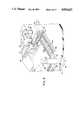
- FIG. 1Shown in FIG. 1 is a connection system for connecting a multi-chip module 10 to a printed circuit board 12.
- This connection systemutilizes a rectangular array of four pairs of flexible circuits 14 and 16, with support subassembly 17, module clamp plate 18 and assembly clamp plate 20.
- the support subassembly 17includes module base plate 22 and four circuit blocks 24. Secured between each circuit block 24 and module base plate 22 are silicone foam strip 26 and an actuator plate 28, one actuator plate 28 per circuit block 24.
- On the bottom of each circuit block 24is another silicone foam strip 30 which is used to generate contact force between contact pads 56 on flex circuits 14, 16 and contact pads on printed circuit board 12.
- each flex circuit 14, 16is secured to the top of module base plate 22 with the silicone foam strip 3 underneath its contact pads and its other end is secured to the bottom of a corresponding circuit block 24 against a silicone foam strip 30.
- This connector systemis designed to complete pressure-mated electrical circuits between pads 60 on one end of each flex circuit 14, 16 with contact pads on module 10 without wipe, and wiping connections between contact pads on the other end of each flex circuit 14, 16 and contact pads 56 on the printed wiring board 12.
- each flex circuit 14, 16can be connected at very high density.
- the spacing of contact pads on module 10is 0.012 inch center to center spacing and the center to center spacing of contacts 56P for the wiping connections on the printed wiring board 12 is 0.025 inch.
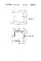
- FIGS. 2A and 2BThe mechanism used to create wiping motion of flex circuit contact pads with pads 56 on the printed circuit board surface is shown in FIGS. 2A and 2B.
- FIG. 2Ashows the clamped position of multi-chip module 10 on module base plate 22 and the cross-section of assembly components in an unclamped position with actuator plate 28 mounted between module base plate 22 and circuit block 24; and
- FIG. 2Bshows the cross-section of assembly components in a clamped position.
- Contact pads on module 10are in contact with the contact pads 60 on the flex circuits 14 and 16 and the silicone foam piece 32 is compressed beneath the flex circuits 14, 16, with the module 10 on top and the module base plate 22 underneath, to create the contact force for the module contact pad connection.
- the clamping forceis generated by the module clamping plate 18 as a result of engagement with the module connection posts 34 in the module base plate 22.
- the mechanism which creates this clamping forceis shown in a cut-away view in FIG. 3, which is an enlarged view of a portion of from FIG. 1, showing the module base plate 22 with upstanding post 34 and a cut-away view of a ramp surface 40 in the module clamp plate 18.
- the ramp and post clamping mechanismis shown in more detail in FIGS. 3A, B, C and D. Ramp and post mechanisms are used both to clamp the multi-chip module 10 to the module base plate 22 and also to clamp subassembly 17 onto the printed circuit board 12 by using assembly clamp plate 20.
- Both the module clamping plate 18 and assembly clamp plate 20include elongated slots 35 with ramp surfaces 40 that interact with the shoulders 42 of posts 34 of the module base plate 22 and shoulders 42 of posts 36 of backplate 38 (FIG. 2A).
- Each ramp 40 of plates 18 and 20has dual angles (lateral and longitudinal tapers) that interact with the angled shoulder portion 42 of posts 34 and 36.
- FIGS. 3A, B and CThe relationships between unclamped and clamped stages for both the module clamping plate 18 and assembly clamping plate 20 are shown in FIGS. 3A, B and C; and FIG. 3D (a cross-sectional view of FIG.
- 3Cshows the relationship of posts 34 and 36 to the clamp plates 18 and 20 in the clamped position and also shows the laterally inclined aspects of ramp portions 40 and latch portion 44, the longitudinal ramp portions 40 of plates 18 and 20 being at the same angle as the shoulder angle portions 42 of each post 34, 36. During clamping of either of these assemblies, the posts slide smoothly along the ramps.
- angles of both the beveled portions 42 of posts 34 and 36, and portions 40, 44 of clamp plates 1 and 20are all provided with 20° angles to the horizontal.
- arrow Aindicates lateral motion of clamp plate 18 or 20 during the clamping interaction of surfaces 40. 42 and 44.
- Motion Agenerates downward motion B of the clamp plates 18 and 20.
- the relationship of motion A to motion Bis the same for both module clamp plate 18 and assembly clamp plate 20.
- the downward motion Bis 0.060 inch in both cases while the linear motion A is about 0.110 inch.
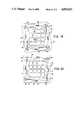
- FIG. 4is a top view of multi-chip module 10 showing, for example, sixteen chips 46 of an arbitrary size. In this case the module is three inches on the side and has a 0.096 inch diameter hole 4 in each corner.
- the connection systemthus provides space for chips or other components on the bottom side of module 10 as well as on its top side. There is space to put components on the top surface of the printed circuit board 12 in its center region, as well.
- FIG. 5shows contact pad arrays 50. There are two groups of contact pad arrays on each side of the module for a total of eight contact pad arrays 50.
- Each of these contact pad arraysmate with one end of each of the flex circuits 14 and 16.
- Each of these contact pad arrays 50have one hundred contact pads 50P for signals at 0.012 inch centers and a ground strip connection 50G.
- the ground strip connection 50Gis located to the outboard side of the module 10, providing a significant convenience in routing as it is significantly more convenient to have the signal pads 50P on the inboard side of the ground strip connection 50G.
- FIG. 6is a top plan view of the printed circuit board 12 and shows four contact pad arrays 56, one on each side of a square shape. In the corners between each contact pad array 56 is an alignment hole 52 which fits over backplate clamp posts 36, not shown in this drawing. There are also slots 54 used to allow space for the circuit mounting posts 58, not shown in this drawing, see FIG. 13.
- Each contact array 56consists of two rows of contact pads 56P and two ground contact strips 56G. The order from inboard to outboard is a row of contact pads 56P B , a ground strip 56G B , a second row of contact pads 56P A and a further ground strip 56G A . There are a hundred contact pads 56P in each row at 0.025 inch center to center spacing.
- each row of contact padsthere are circular pads 56R for plated-through-holes to bring the signals from the contact pads 56P to internal circuit layers of the board 12. These contact pads 56R are offset in an alternating array to minimize the space consumed.
- the clearance holes 52 for the backer plate mounting posts 36are 0.206 inches in diameter, and the slots 54 for clearance of the circuit mounting posts 58 are 0.025 inch wide by 0.116 inch long.
- FIGS. 7A and 7Bshow flex circuits 14 and 16 of which two are used per side of the four-sided module, for a total of eight. These circuits have contact arrays 60, 62 at each end with traces 61 connecting the contact pads. At the narrow end of each circuit 14, 16 is contact array 60 which mates with contact array 50 on the multi-chip module 10 and at the wide end is contact array 62 which mates with part of the contact array 56 on the printed wiring board 12. Flex circuit 16, which is shown in 7B, is shorter than flex circuit 14 so that contact arrays 62B are offset slightly at the board end to overlap, and array 62A matches with one half (56A) of contact pad array 56 and array 62B matches with the other half (56B).
- each flex circuit 14facing outboard of the contact array is a tab 68 which has a 0.125 inch diameter hole designed to press fit over the post 34 in the module plate 22, and at each end of the narrow end of each flex circuit 14, 16 is a tab with a 0.094 inch hole 66 which is designed to press fit over module alignment posts 70 in the module base plate 22.
- a similar tabwhich contains a 0.094 inch diameter hole 64 which is designed to press fit over circuit block mounting posts 58 which are shown in FIG. 11.
- FIG. 8shows an enlarged plan view of a crenellated contact pad 62P of contact array 62, that is used on the wide ends of the flex circuits 14, 16.
- the contact pads 56P on the printed wiring board 12 for which these crenellated contacts 62P are to be connectedare plain rectangular pads 0.100 inch long by 0.010 inch wide.
- the contact pads 60P at the narrow ends of the flex circuits 14, 16are 0.050 inch long and approximately 0.006 inch wide at 0.012 inch center to center spacing, the same pad spacing that is on module 10.
- FIG. 9Ashows a top plan view of module base plate 22 and FIG. 9B shows a bottom plan view of plate 22.
- the overall size of the module base plate 22is about four inches by about four inches square and it is 0.150 inch thick.
- a 0.206 inch diameter clearance hole 76that fits down over a backer plate clamp post 36.
- the square opening in the center of the module base plate 22is 2.7 inches by 2.7 inches with a small chamfer in each corner. Slightly outboard of each chamfer in each corner is a 0.094 inch diameter module alignment post 70 that fits into a corner hole 48 in module 10.
- FIG. 9Bis a bottom plan view of module plate 22.
- assembly stop 78On each of the four sides of the bottom surface of plate 22 are the following features, going from the inboard side of the module base plate to the outboard side: assembly stop 78; mounting recess 80 for resilient wiping control return strip 26; operating cavity 82 for actuator plate 28, retaining lip 80 and assembly stop 84.
- FIG. 10shows a top plan view of module base plate 22 with flex circuits 14, 16 mounted in place.
- Tabs with holes 66A and 66Bare mounted over the module alignment posts 70, and tabs with press fit holes 68A and 68B are mounted over the module base plate shoulder posts 34, so that pairs of contact arrays 60A, 60B are fixed in end to end alignment over silicone foam strips 32.
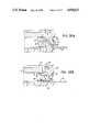
- FIG. 12is an exploded isometric view, showing a portion of a circuit block 24 and foam pieces 22, 26, and 30.
- One of these circuit blocks 24is mounted to each of the four sides of the module base plate 22.
- Each circuit block 24, as shown in FIG. 11,has the following features from the inboard side to the outboard side of the circuit block: assembly stop 86 which matches with the assembly stop 78 on the module base plate, mounting recess 88 for the foam piece 26, which lines up opposite the mounting recess 80, retaining lip 90, which retains the other end of the actuator plate 28 from retaining lip 83 in the module base plate, recess 92, an assembly stop 94 which matches with assembly stop 84 in the module base plate.
- assembly stop 86which matches with the assembly stop 78 on the module base plate
- mounting recess 88 for the foam piece 26which lines up opposite the mounting recess 80
- retaining lip 90which retains the other end of the actuator plate 28 from retaining lip 83 in the module base plate
- recess 92recess 92
- an assembly stop 94which matches with assembly stop 84 in the module base plate.
- each end of the circuit blocknecks down to a smaller thickness creating tabs 98, 100.
- tab portion 98overlies tab portion 100 of an adjacent circuit block.
- Each circuit blockhas a tab portion 98 on the upper side and tab 100 at the opposite end on the lower side.
- Tab portions 98, 100have slots 96, which are 0.206 inch wide by 0.241 inch long, and fit over backer plate clamping posts 36 and function as a stop when the slot 96 is forced by the circuit block wiping motion up against the post 36 to fix the position of that circuit block relative to circuit board 12.
- the tab portion 100, at the other end of each circuit blockhas a slot 102, not shown in FIG. 12, which is 0.216 inch wide by 0.241 inch long.
- FIG. 12also shows backer plate 38 with the shoulder mounting clamping posts 36, and the printed circuit board 12, with the holes 52 which fit over the backer plate post 36.
- FIG. 12also shows in phantom, a circuit mounting post 58 of which there are two on each circuit block 24.
- the circuit mounting posts 58are designed to press fit into the holes 64, 64 in the tabs of the wide ends of the flex circuits 14 and 16.
- the clearance slots 54 in the printed circuit board 12, also shown in FIG. 6,allow clearance for posts 58.
- FIG. 13is a bottom view of subassembly 17 that includes module base plate 22, circuit blocks 24 and flex circuits 14 and 16, there being four circuit blocks 24, four flex circuits 14 and four flex circuits 16 in subassembly 17.
- FIG. 14is a top view of subassembly 17 with multi chip module 10 mounted on top. Alignment holes 48 in the four corners of the multi chip module 10 are mounted over alignment posts 70 of module base plate 22.
- FIG. 15is a top plan view of module clamp plate 18.
- each tab 110containing ramp structure as shown in FIGS. 3A, B, C, and D. That structure includes opening 39 for shouldered post 34 of the module base plate 22, inclined ramp sections 40, and latch section 44, the latter in the final position, being mated against the shoulder 42 of the clamp post 34.
- Clamp plate 18has an inside opening of approximately 2.5 inches square shape with beveled angle 104 at each corner, and inside edge 106 at an angle to the square to allow clearance for components 46 mounted on the multi chip module. Additionally, the outside corners of the module clamp plate 18 are beveled, along edges 108, to allow clearance for module alignment posts 70.
- FIG. 16is a top plan view with the multi chip module 10 mounted on top of the subassembly 17 and the module clamp plate 18 mounted on top of the multi chip module. in its unclamped position.
- FIG. 17shows the components of FIG. 16 with plate 18 rotated into clamped position. The clamping action engages ramps 40 of clamp plate 18 with the shoulder posts 34 of base plate 22, causing downward motion of the module clamp plate 18, which presses multi chip module 10 down upon the module base plate 22, clamping the flex circuit pads 60P, 60G against corresponding pads 50P, 50G of module 10, and compressing silicone foam strip 32 so that electrical contacts between the contact arrays 50 on the bottom of multi chip module 10 and contact arrays 60 of the narrow end of the flex circuits 14, 16 are completed.
- FIG. 18Ais a top plan view of the assembly clamp plate 20.
- the slotted ramp structuresof the type shown in FIGS. 3A, B, C, and D.
- Each hole 39'fits over a backer plate mounting post 36, and has a ramp section 40', which engages the shoulder 42 of the backer plate post 36.
- the inside opening of the assembly clamp plateis approximately square, with a curved relieved section 112 in the center of each side which provides space to accommodate the projecting tab portion 110 of the module clamp plate 18.
- Assembly clamp plate 20also has a bevelled portion 114 in each corner, and an angled side portion 116 for clearance around corners of multi-chip module 10.
- FIG. 19shows in top plan view, the entire assembly in position to be clamped to printed circuit board 12 with backer plate 38, subassembly 17 mounted over assembly mounting posts 36, module 10 having been connected by module clamping plate 18, and assembly clamp plate 20, in position on top of subassembly 17, fitting over mounting posts 36.
- FIG. 20shows the entire assembly in clamped position.
- assembly clamp plate 20When subassembly 17 is to be clamped to the printed circuit board 12 using the assembly clamp plate 20, as assembly clamp plate 20 is rotated, mounting posts 36 in backup plate 38 are engaged. This engagement produces a downward motion of the assembly clamp plate 20, which in turn presses down and causes downward motion of module base plate 22, of about 0.060 inch.
- module base plate 22is pressed towards printed circuit board 10, causing pinless hinge actuator members 28 to press against the circuit blocks 24, causing the circuit blocks 24 to move sideways in wiping actions across the surface of the printed wiring board 12.
- silicone foam strip 26is both compressed and stressed under shear. This creates and controls the downward force during the wiping motion and creates a return force so that when the system is demated, the components return to their original unclamped position.
- the silicone foam 30which is used to create the contact force on the printed wiring board. As the system is compressed, the foam strip 30 is compressed and generates contact force.
- circuit blocks 24At the end of this downward motion of module clamp plate 22, the circuit blocks 24 have been moved inward about 0.035 inch and the assembly stop surfaces 86 an 78, are in contact, as are assembly stop surfaces 94 and 84. At this time elastomer strip 30 has been compressed 0.040 inch, thus making wipe connections between flex circuits 14 and 16 and printed circuit board 12.
- circuit blocks 24can be controlled during wipe by varying certain parameters. Among these are the physical properties and geometries of foam members 26 and 30. Upon completion of wipe, elastomer member 26 is under shear stress. When circuit blocks 24 are released by rotating assembly clamp plate 20 to the pre-clamp position of FIG. 19, the circuit blocks 24 are returned by release of the shear stress to their preclamped position.
- the amount of wipe and the force vs. wipe profilecan also be varied by varying the geometry and angle of the actuator mechanism previously described.
- module base plate 22is forced downward by the downward motion of assembly clamp plate 20
- module base plate 22is held rigidly in lateral position by the four backer plate clamp posts 36.
- the actuator member 28, which is rigid,is held at one end by retaining lip 83 in the module base plate 22, and by retaining lip 90 in the circuit block 24 at the other end.
- Circuit block 24is free to move laterally, under the restraint of silicone foam mounting member 26. Lateral motion of circuit block 24 creates resilient shear stress on the silicone foam member 26.
- the rigid actuator member 28is caused to rotate. Since the module base plate 22 is rigidly restrained in the horizontal axis, this rotation of rigid pinless hinge member 28 causes circuit block 24 to move laterally.
- the flexible circuitsextend from the perimeter of the multi-chip module inwardly and then extend outwardly to the perimeter of the contact pads on the surface of the circuit board; and the circuit blocks are moved inwardly towards the center of the assembly by the wiping action.
- the unitary clamp member with the slotted ramp arrangementprovides a mechanically simple arrangement that allows quick and easy mating and demating of the components.
- Such unitary clamp membermay move in straight line movement, but in preferred embodiments is rotated such that the clamp plate provides simultaneous downward forces on the surfaces of the hardware assembly which is to be clamped.
- the connector arrangementpermit a number of elements to control the amount of wipe and contact force generate as a function of wiping movement, such that the system may be designed for various specific applications and needs.
- FIGS. 2lA and 2lBAnother embodiment is shown in FIGS. 2lA and 2lB, that embodiment employs a leaf spring member 130 that extends between post 132 on module plate 22' and post 134 of contact lock 24'.
- leaf spring member 130that extends between post 132 on module plate 22' and post 134 of contact lock 24'.
- leaf spring 130As leaf spring 130 is compressed, it tends to elongate.
- contact block 24'is free to move laterally, as controlled by the leaf spring 130, there is wiping action on the pressure-mated contact pads of flex circuits 14', 16', and the engaged contact pads 56 of circuit board 12'.
- leaf spring 130can be varied as desired to vary the amount of force transmitted to the circuit block 24 by the module plate 21' to vary the force versus wipe profile.
- FIGS. 22A and 22BStill another embodiment is shown in FIGS. 22A and 22B, again similar to FIGS. 2A and 2B showing the connector assembly in unclamped position and clamped position.
- cam post 140extends downwardly from clamp ring 20" with its lower end received in camming slot 142 of contact block 24". That groove 142 is elongated and has upstanding surface 144 against which the edge of camming post 140 bears.
- the cam posts 140move along cam grooves 142, camming the circuit block 24" inwardly causing wiping interaction between contact pads on flex circuits 14", 16" and contact pads on circuit board 12".
- the posts 140could be integral with contact block 24" and engaged in a camming groove in clamp plate 20".
- FIG. 18Bshows assembly clamp plate structure 20" suitable for use in a modified embodiment in which two clamp plate structures 20A and 20B are employed, each structure including two depending cam posts 140 that cooperate with camming slots 142.
- connection systemprovides a high density, electrically superior interconnection to both the module 10 and to the printed circuit board 12.
- the use of flex circuits 14, 16 with fluoropolymer materialsprovides excellent high frequency electrical performance.
- the pressure-mated pad connection between flex circuits 14, 16 and multi-chip module 10 printed circuit 12provides electrically superior interconnection that does not produce significant electrical discontinuities even at high frequencies.
- the disclosed embodimentsprovide a dense interconnection, in terms of number of signals per area consumed, on the surface of multi-chip module 10. They also have the advantage of being a simple connection to mate and de-mate. As it does not involve solder, the risk of heating the interface when mating or de-mating the connection is not involved and those components may be separated easily for repair or component replacement.
- the ground connection for the flex circuitis located on the outboard side of the module, simplifying routing of the signal contacts by permitting the rows of contact pads to be on the inboard side of the module from the ground connection.
- the embodimentpermits close contact spacing, e.g., contacts on 0.012 inch centers, so eight hundred signal contacts can easily be provided on a 3-inch by 3-inch module, leaving approximately a 2-1/2-inch square central space for mounting chips or other components on both the top and the bottom surfaces of the module.
- close contact spacinge.g., contacts on 0.012 inch centers
- eight hundred signal contactscan easily be provided on a 3-inch by 3-inch module, leaving approximately a 2-1/2-inch square central space for mounting chips or other components on both the top and the bottom surfaces of the module.
- the preferred embodimentprovides a non-wiping pressure mated pad connection on module 10.
- a wiping connectionis not needed at the module end because such modules are generally tested and repaired, if necessary, or inspected in a clean room environment.
- a wiping connectioncould be provided at the module end for the high density contacts where desired.
- the wiping connection of the disclosed embodimentis desirable from an environmental standpoint.
- the systemprovides the wiping contact on the printed circuit board which is also easily matable-dematable without solder and also provides a dense connection in terms of number of signals per area taken up on the board. While the contact density on the board is less than on the module the density capabilities on the circuit end and on the module end match well with presently existing manufacturing capabilities. For a three-by-three inch module in this preferred embodiment, a square space approximately 2-1/2 inches per side is available on each side of the module for other components besides the connection, while still providing eight hundred contacts (290 contacts per square inch of module surface area).
- the slotted ramp mechanism for providing clamping forcehas the advantages of being very simple mechanically and allowing quick and easy mate and demate of the components, whether by the rotating movement in the preferred embodiment or in lateral or other clamping plate member movements.
- the platepreferably provides simultaneous downward force on the entire surface of the hardware assembly which is clamped.
- the wiping mechanismallows a number of elements to control the amount of wipe, and the contact force generated as a function of the wiping movement, which allows the system to be easily accommodated to various specific applications and needs.
- the silicone foam materialhas high stress retention even at elevated temperatures.
- Other componentssuch as the clamping plates, the circuit blocks, the module base plate, and the actuator hinge, are preferably molded compounds for cost savings and weight considerations, although machined metal may be used. Preferably, these are formed of glass-reinforced phenolic, molded into the required shapes.
- the multi-chip moduleis a multi-layer ceramic material
- the printed circuit boardis a multi-layer epoxy-glass board or a multi-layer fluoropolymer board.
- the flexible circuitspreferably include a fluoropolymer material such as Rogers RO2500 for its high frequency and lack of water absorption advantages, and are of controlled impedance to match the impedance of the module and the board assembly.
- the high density connection systemwill employ a multilayer circuit board 12, as discussed. Frequently, it will be o such a large number of layers that its thickness and rigidity is sufficient to provide the needed rigidity of the system. In such cases a backer plate may be unnecessary; the assembly backer plate clamp posts being mounted directly into the printed circuit board.
- Another advantage of the present systemis the elimination of separate stops for each of the circuit blocks 24.
- Each fixed corner post 36stops the ends of the two overlapping circuit blocks, reducing the number of hardware parts.
Landscapes
- Engineering & Computer Science (AREA)
- Microelectronics & Electronic Packaging (AREA)
- Coupling Device And Connection With Printed Circuit (AREA)
- Multi-Conductor Connections (AREA)
Abstract
Description
Claims (36)
Priority Applications (4)
| Application Number | Priority Date | Filing Date | Title |
|---|---|---|---|
| US07/154,197US4830623A (en) | 1988-02-10 | 1988-02-10 | Connector arrangement for electrically interconnecting first and second arrays of pad-type contacts |
| JP1502308AJPH02503134A (en) | 1988-02-10 | 1989-02-10 | connector structure |
| EP19890902476EP0356490A4 (en) | 1988-02-10 | 1989-02-10 | Connector arrangement |
| PCT/US1989/000554WO1989007845A1 (en) | 1988-02-10 | 1989-02-10 | Connector arrangement |
Applications Claiming Priority (1)
| Application Number | Priority Date | Filing Date | Title |
|---|---|---|---|
| US07/154,197US4830623A (en) | 1988-02-10 | 1988-02-10 | Connector arrangement for electrically interconnecting first and second arrays of pad-type contacts |
Publications (1)
| Publication Number | Publication Date |
|---|---|
| US4830623Atrue US4830623A (en) | 1989-05-16 |
Family
ID=22550390
Family Applications (1)
| Application Number | Title | Priority Date | Filing Date |
|---|---|---|---|
| US07/154,197Expired - Fee RelatedUS4830623A (en) | 1988-02-10 | 1988-02-10 | Connector arrangement for electrically interconnecting first and second arrays of pad-type contacts |
Country Status (4)
| Country | Link |
|---|---|
| US (1) | US4830623A (en) |
| EP (1) | EP0356490A4 (en) |
| JP (1) | JPH02503134A (en) |
| WO (1) | WO1989007845A1 (en) |
Cited By (25)
| Publication number | Priority date | Publication date | Assignee | Title |
|---|---|---|---|---|
| US5057025A (en)* | 1989-08-23 | 1991-10-15 | Stocko Metallwarenfabriken Henkels Und Sohn Gmbh & Co. | Display contacts |
| US5186632A (en)* | 1991-09-20 | 1993-02-16 | International Business Machines Corporation | Electronic device elastomeric mounting and interconnection technology |
| GB2260657A (en)* | 1991-10-16 | 1993-04-21 | Whitaker Corp | Electrical socket for electronic package |
| US5266059A (en)* | 1992-09-08 | 1993-11-30 | Hewlett-Packard Company | Generic rotatable connector assembly for testing integrated circuit packages |
| US5267867A (en)* | 1992-09-11 | 1993-12-07 | Digital Equipment Corporation | Package for multiple removable integrated circuits |
| US5468996A (en)* | 1994-03-25 | 1995-11-21 | International Business Machines Corporation | Electronic package assembly and connector for use therewith |
| WO1996002913A1 (en)* | 1994-07-15 | 1996-02-01 | Berg Technology, Inc. | Long arm compression connector with bump header |
| US5539621A (en)* | 1994-01-14 | 1996-07-23 | Elonex Technologies, Inc. | Network communication unit with client and resource node array double layer ICs on printed board with connectors on housing |
| USRE35733E (en)* | 1991-11-26 | 1998-02-17 | Circuit Components Incorporated | Device for interconnecting integrated circuit packages to circuit boards |
| US5785535A (en)* | 1996-01-17 | 1998-07-28 | International Business Machines Corporation | Computer system with surface mount socket |
| US5919050A (en)* | 1997-04-14 | 1999-07-06 | International Business Machines Corporation | Method and apparatus for separable interconnecting electronic components |
| US5921786A (en)* | 1997-04-03 | 1999-07-13 | Kinetrix, Inc. | Flexible shielded laminated beam for electrical contacts and the like and method of contact operation |
| WO2000021131A1 (en)* | 1998-10-07 | 2000-04-13 | Ferraz Shawmut | Method for mounting an electric of electronic installation and heat exchanger for power electrical or electronic components |
| US6102710A (en)* | 1992-08-05 | 2000-08-15 | Fujitsu Limited | Controlled impedance interposer substrate and method of making |
| WO2001008187A1 (en)* | 1999-07-23 | 2001-02-01 | Lockheed Martin Corporation | Reconfiguragle multichip module stack interface |
| US6490725B2 (en) | 1994-01-14 | 2002-12-03 | Elonex I.P. Holdings, Ltd. | Transmitting notification of new video clips of interest from servers in wide area network |
| US20050014396A1 (en)* | 2003-07-14 | 2005-01-20 | Fci Americas Technology, Inc. | Electrical contact assembly with insulative carrier, stapled contact attachment and fusible element |
| US20080057750A1 (en)* | 2006-09-01 | 2008-03-06 | Hon Hai Precision Ind. Co., Ltd. | Socket connector with retaining device |
| US7405940B1 (en)* | 2007-04-25 | 2008-07-29 | International Business Machines Corporation | Piston reset apparatus for a multichip module and method for resetting pistons in the same |
| US20100175242A1 (en)* | 2009-01-12 | 2010-07-15 | Tong Hsing Electric Industries Ltd. | Method for packaging micro electromechanical systems microphone |
| US20110306251A1 (en)* | 2010-06-14 | 2011-12-15 | Tyco Electronics Corporation | Connector with a laterally moving contact |
| US20120275634A1 (en)* | 2011-04-26 | 2012-11-01 | Epcos Ag | Mems microphone |
| US20130167663A1 (en)* | 2011-09-30 | 2013-07-04 | Sensitronics, LLC | Hybrid Capacitive Force Sensors |
| CN114770971A (en)* | 2022-04-27 | 2022-07-22 | 郑州大学 | Foam filling bionic lattice composite structure and preparation method thereof |
| US12444866B2 (en)* | 2019-03-14 | 2025-10-14 | Te Connectivity Solutions Gmbh Et Al. | Electrical connector system |
Citations (32)
| Publication number | Priority date | Publication date | Assignee | Title |
|---|---|---|---|---|
| US31114A (en)* | 1861-01-15 | Improvement in grain-separators | ||
| US1610555A (en)* | 1920-03-01 | 1926-12-14 | Westinghouse Electric & Mfg Co | Voltage-regulator system |
| US3173737A (en)* | 1963-08-05 | 1965-03-16 | Amp Inc | Connector with tab terminal latching means |
| US3356983A (en)* | 1965-10-11 | 1967-12-05 | Ibm | Transmission line cable connector |
| US3582865A (en)* | 1969-12-16 | 1971-06-01 | Ibm | Microcircuit module and connector |
| US3587031A (en)* | 1969-10-02 | 1971-06-22 | Ibm | Electrical connector housing with means producing contact wipe |
| US3597660A (en)* | 1969-12-10 | 1971-08-03 | Ibm | High-density circuits connector |
| US3701964A (en)* | 1970-09-04 | 1972-10-31 | Lockheed Aircraft Corp | Flat cable electrical wiring system |
| US3745509A (en)* | 1971-03-02 | 1973-07-10 | Bunker Ramo | High density electrical connector |
| US3873173A (en)* | 1973-10-05 | 1975-03-25 | Itt | Electrical connector assembly |
| US3999826A (en)* | 1975-06-30 | 1976-12-28 | General Motors Corporation | Connector for flexible printed circuit |
| US4092057A (en)* | 1975-08-28 | 1978-05-30 | Burroughs Corporation | Flexible circuit assembly |
| US4116517A (en)* | 1976-04-15 | 1978-09-26 | International Telephone And Telegraph Corporation | Flexible printed circuit and electrical connection therefor |
| US4164003A (en)* | 1976-12-27 | 1979-08-07 | Cutchaw John M | Integrated circuit package and connector therefor |
| US4169642A (en)* | 1976-09-16 | 1979-10-02 | E. I. Du Pont De Nemours And Company | Integrated circuit connector |
| US4330163A (en)* | 1979-12-05 | 1982-05-18 | E. I. Du Pont De Nemours And Company | Zero insertion force connector for LSI circuit package |
| USRE31114E (en) | 1975-11-13 | 1982-12-28 | Tektronix, Inc. | Electrical connector |
| US4392700A (en)* | 1981-09-08 | 1983-07-12 | Amp Incorporated | Cam actuated zero insertion force mother/daughter board connector |
| US4420203A (en)* | 1981-06-04 | 1983-12-13 | International Business Machines Corporation | Semiconductor module circuit interconnection system |
| US4511197A (en)* | 1983-08-01 | 1985-04-16 | Amp Incorporated | High density contact assembly |
| US4540227A (en)* | 1984-03-21 | 1985-09-10 | Grumman Aerospace Corporation | Test equipment interconnection system |
| US4553192A (en)* | 1983-08-25 | 1985-11-12 | International Business Machines Corporation | High density planar interconnected integrated circuit package |
| US4552420A (en)* | 1983-12-02 | 1985-11-12 | E. I. Du Pont De Nemours And Company | Electrical connector using a flexible circuit having an impedance control arrangement thereon |
| US4602317A (en)* | 1984-12-13 | 1986-07-22 | Gte Communication Systems Corporation | Printed wiring board connector |
| US4626056A (en)* | 1984-02-21 | 1986-12-02 | Amp Incorporated | Card edge connector |
| US4629270A (en)* | 1984-07-16 | 1986-12-16 | Amp Incorporated | Zero insertion force card edge connector with flexible film circuitry |
| US4636019A (en)* | 1984-02-06 | 1987-01-13 | International Business Machines Corporation | Connector mechanisms |
| US4647125A (en)* | 1985-07-22 | 1987-03-03 | Rogers Corporation | Solderless connector technique |
| US4655524A (en)* | 1985-01-07 | 1987-04-07 | Rogers Corporation | Solderless connection apparatus |
| US4690472A (en)* | 1986-09-26 | 1987-09-01 | E. I. Du Pont De Nemours And Company | High density flex connector system |
| US4695258A (en)* | 1986-12-09 | 1987-09-22 | Cherne Industries, Inc. | Connector assembly for electrically connecting flexible and rigid printed circuits |
| US4717345A (en)* | 1985-07-22 | 1988-01-05 | Rogers Corporation | Solderless connector technique and apparatus |
Family Cites Families (2)
| Publication number | Priority date | Publication date | Assignee | Title |
|---|---|---|---|---|
| US4341432A (en)* | 1979-08-06 | 1982-07-27 | Cutchaw John M | Liquid cooled connector for integrated circuit packages |
| US4593961A (en)* | 1984-12-20 | 1986-06-10 | Amp Incorporated | Electrical compression connector |
- 1988
- 1988-02-10USUS07/154,197patent/US4830623A/ennot_activeExpired - Fee Related
- 1989
- 1989-02-10EPEP19890902476patent/EP0356490A4/ennot_activeWithdrawn
- 1989-02-10JPJP1502308Apatent/JPH02503134A/enactivePending
- 1989-02-10WOPCT/US1989/000554patent/WO1989007845A1/ennot_activeApplication Discontinuation
Patent Citations (32)
| Publication number | Priority date | Publication date | Assignee | Title |
|---|---|---|---|---|
| US31114A (en)* | 1861-01-15 | Improvement in grain-separators | ||
| US1610555A (en)* | 1920-03-01 | 1926-12-14 | Westinghouse Electric & Mfg Co | Voltage-regulator system |
| US3173737A (en)* | 1963-08-05 | 1965-03-16 | Amp Inc | Connector with tab terminal latching means |
| US3356983A (en)* | 1965-10-11 | 1967-12-05 | Ibm | Transmission line cable connector |
| US3587031A (en)* | 1969-10-02 | 1971-06-22 | Ibm | Electrical connector housing with means producing contact wipe |
| US3597660A (en)* | 1969-12-10 | 1971-08-03 | Ibm | High-density circuits connector |
| US3582865A (en)* | 1969-12-16 | 1971-06-01 | Ibm | Microcircuit module and connector |
| US3701964A (en)* | 1970-09-04 | 1972-10-31 | Lockheed Aircraft Corp | Flat cable electrical wiring system |
| US3745509A (en)* | 1971-03-02 | 1973-07-10 | Bunker Ramo | High density electrical connector |
| US3873173A (en)* | 1973-10-05 | 1975-03-25 | Itt | Electrical connector assembly |
| US3999826A (en)* | 1975-06-30 | 1976-12-28 | General Motors Corporation | Connector for flexible printed circuit |
| US4092057A (en)* | 1975-08-28 | 1978-05-30 | Burroughs Corporation | Flexible circuit assembly |
| USRE31114E (en) | 1975-11-13 | 1982-12-28 | Tektronix, Inc. | Electrical connector |
| US4116517A (en)* | 1976-04-15 | 1978-09-26 | International Telephone And Telegraph Corporation | Flexible printed circuit and electrical connection therefor |
| US4169642A (en)* | 1976-09-16 | 1979-10-02 | E. I. Du Pont De Nemours And Company | Integrated circuit connector |
| US4164003A (en)* | 1976-12-27 | 1979-08-07 | Cutchaw John M | Integrated circuit package and connector therefor |
| US4330163A (en)* | 1979-12-05 | 1982-05-18 | E. I. Du Pont De Nemours And Company | Zero insertion force connector for LSI circuit package |
| US4420203A (en)* | 1981-06-04 | 1983-12-13 | International Business Machines Corporation | Semiconductor module circuit interconnection system |
| US4392700A (en)* | 1981-09-08 | 1983-07-12 | Amp Incorporated | Cam actuated zero insertion force mother/daughter board connector |
| US4511197A (en)* | 1983-08-01 | 1985-04-16 | Amp Incorporated | High density contact assembly |
| US4553192A (en)* | 1983-08-25 | 1985-11-12 | International Business Machines Corporation | High density planar interconnected integrated circuit package |
| US4552420A (en)* | 1983-12-02 | 1985-11-12 | E. I. Du Pont De Nemours And Company | Electrical connector using a flexible circuit having an impedance control arrangement thereon |
| US4636019A (en)* | 1984-02-06 | 1987-01-13 | International Business Machines Corporation | Connector mechanisms |
| US4626056A (en)* | 1984-02-21 | 1986-12-02 | Amp Incorporated | Card edge connector |
| US4540227A (en)* | 1984-03-21 | 1985-09-10 | Grumman Aerospace Corporation | Test equipment interconnection system |
| US4629270A (en)* | 1984-07-16 | 1986-12-16 | Amp Incorporated | Zero insertion force card edge connector with flexible film circuitry |
| US4602317A (en)* | 1984-12-13 | 1986-07-22 | Gte Communication Systems Corporation | Printed wiring board connector |
| US4655524A (en)* | 1985-01-07 | 1987-04-07 | Rogers Corporation | Solderless connection apparatus |
| US4647125A (en)* | 1985-07-22 | 1987-03-03 | Rogers Corporation | Solderless connector technique |
| US4717345A (en)* | 1985-07-22 | 1988-01-05 | Rogers Corporation | Solderless connector technique and apparatus |
| US4690472A (en)* | 1986-09-26 | 1987-09-01 | E. I. Du Pont De Nemours And Company | High density flex connector system |
| US4695258A (en)* | 1986-12-09 | 1987-09-22 | Cherne Industries, Inc. | Connector assembly for electrically connecting flexible and rigid printed circuits |
Non-Patent Citations (14)
| Title |
|---|
| "A New Generation in Interconnection Technology", Augaut/Microtec, dated 9/84. |
| A New Generation in Interconnection Technology , Augaut/Microtec, dated 9/84.* |
| Abbatecola et al., IBM Technical Disclosure Bulletin (Mar. 1968) vol. 10, No. 10, p. 1462.* |
| Burke, "Flex Circuit Zero Insertion Force Connector", IBM Technical Disclosure Bulletin, vol. 26, No. 12 (May 1984), p. 6657. |
| Burke, Flex Circuit Zero Insertion Force Connector , IBM Technical Disclosure Bulletin, vol. 26, No. 12 (May 1984), p. 6657.* |
| Connecting Devices Bulletin, Oct. 1976 (3 pages) Hughes Aircraft Co.* |
| Gordon, Backplane Interconnection System, presented at International Electronic Packaging Society Symposium, San Diego, California (Nov. 1986).* |
| Lockard, "System Approach to High-Speed Digital Packaging", reprinted from Electronics Packaging and Production (Sep. 1986). |
| Lockard, System Approach to High Speed Digital Packaging , reprinted from Electronics Packaging and Production (Sep. 1986).* |
| Mersereau, Rogers Solderless System, Proceedings of the Fourth International Electronics Packaging Conference, Oct. 1984, pp. 43 53.* |
| Mersereau, Rogers Solderless System, Proceedings of the Fourth International Electronics Packaging Conference, Oct. 1984, pp. 43-53. |
| RSS Rogers Solderless System for Interconnections, Copyright 1979, Rogers Corporation.* |
| RSS™ Rogers Solderless System for Interconnections, Copyright 1979, Rogers Corporation. |
| Simpson et al., Connector with High Contact Density and Controlled Impedance.* |
Cited By (41)
| Publication number | Priority date | Publication date | Assignee | Title |
|---|---|---|---|---|
| US5057025A (en)* | 1989-08-23 | 1991-10-15 | Stocko Metallwarenfabriken Henkels Und Sohn Gmbh & Co. | Display contacts |
| US5186632A (en)* | 1991-09-20 | 1993-02-16 | International Business Machines Corporation | Electronic device elastomeric mounting and interconnection technology |
| GB2260657A (en)* | 1991-10-16 | 1993-04-21 | Whitaker Corp | Electrical socket for electronic package |
| GB2260657B (en)* | 1991-10-16 | 1995-04-12 | Whitaker Corp | Electrical socket |
| USRE35733E (en)* | 1991-11-26 | 1998-02-17 | Circuit Components Incorporated | Device for interconnecting integrated circuit packages to circuit boards |
| US6102710A (en)* | 1992-08-05 | 2000-08-15 | Fujitsu Limited | Controlled impedance interposer substrate and method of making |
| US5266059A (en)* | 1992-09-08 | 1993-11-30 | Hewlett-Packard Company | Generic rotatable connector assembly for testing integrated circuit packages |
| DE4315082A1 (en)* | 1992-09-08 | 1994-03-10 | Hewlett Packard Co | Versatile rotatable connector assembly for testing integrated circuit components |
| NL9300766A (en)* | 1992-09-08 | 1994-04-05 | Hewlett Packard Co | Generally rotatable connection terminal assembly for testing integrated circuit building blocks. |
| US5267867A (en)* | 1992-09-11 | 1993-12-07 | Digital Equipment Corporation | Package for multiple removable integrated circuits |
| US5539621A (en)* | 1994-01-14 | 1996-07-23 | Elonex Technologies, Inc. | Network communication unit with client and resource node array double layer ICs on printed board with connectors on housing |
| US6490725B2 (en) | 1994-01-14 | 2002-12-03 | Elonex I.P. Holdings, Ltd. | Transmitting notification of new video clips of interest from servers in wide area network |
| EP0674472A3 (en)* | 1994-03-25 | 1996-04-03 | Ibm | Electronic package assembly and connector for use therewith. |
| US5468996A (en)* | 1994-03-25 | 1995-11-21 | International Business Machines Corporation | Electronic package assembly and connector for use therewith |
| US5530291A (en)* | 1994-03-25 | 1996-06-25 | International Business Machines Corporation | Electronic package assembly and connector for use therewith |
| WO1996002913A1 (en)* | 1994-07-15 | 1996-02-01 | Berg Technology, Inc. | Long arm compression connector with bump header |
| US5966267A (en)* | 1994-07-15 | 1999-10-12 | Fci Americas Technology, Inc. | Long arm compression connector with bump header |
| US5785535A (en)* | 1996-01-17 | 1998-07-28 | International Business Machines Corporation | Computer system with surface mount socket |
| US5921786A (en)* | 1997-04-03 | 1999-07-13 | Kinetrix, Inc. | Flexible shielded laminated beam for electrical contacts and the like and method of contact operation |
| US5919050A (en)* | 1997-04-14 | 1999-07-06 | International Business Machines Corporation | Method and apparatus for separable interconnecting electronic components |
| FR2784537A1 (en)* | 1998-10-07 | 2000-04-14 | Ferraz | METHOD FOR ASSEMBLING AN ELECTRICAL OR ELECTRONIC POWER INSTALLATION AND HEAT EXCHANGER FOR ELECTRICAL OR ELECTRONIC POWER COMPONENTS |
| WO2000021131A1 (en)* | 1998-10-07 | 2000-04-13 | Ferraz Shawmut | Method for mounting an electric of electronic installation and heat exchanger for power electrical or electronic components |
| WO2001008187A1 (en)* | 1999-07-23 | 2001-02-01 | Lockheed Martin Corporation | Reconfiguragle multichip module stack interface |
| US20050014396A1 (en)* | 2003-07-14 | 2005-01-20 | Fci Americas Technology, Inc. | Electrical contact assembly with insulative carrier, stapled contact attachment and fusible element |
| US6994565B2 (en) | 2003-07-14 | 2006-02-07 | Fci Americas Technology, Inc. | Electrical contact assembly with insulative carrier, stapled contact attachment and fusible element |
| US20080057750A1 (en)* | 2006-09-01 | 2008-03-06 | Hon Hai Precision Ind. Co., Ltd. | Socket connector with retaining device |
| US7476107B2 (en)* | 2006-09-01 | 2009-01-13 | Hon Hai Precision Ind. Co., Ltd. | Socket connector with retaining device |
| US20080264606A1 (en)* | 2007-04-25 | 2008-10-30 | International Business Machines Corporation | Piston reset apparatus for a multichip module and method for resetting pistons in the same |
| US7405940B1 (en)* | 2007-04-25 | 2008-07-29 | International Business Machines Corporation | Piston reset apparatus for a multichip module and method for resetting pistons in the same |
| US7826228B2 (en)* | 2007-04-25 | 2010-11-02 | International Business Machines Corporation | Piston reset apparatus for a multichip module and method for resetting pistons in the same |
| US20100175242A1 (en)* | 2009-01-12 | 2010-07-15 | Tong Hsing Electric Industries Ltd. | Method for packaging micro electromechanical systems microphone |
| US7934306B2 (en)* | 2009-01-12 | 2011-05-03 | Tong Hsing Electric Industries, Ltd. | Method for packaging micro electromechanical systems microphone |
| US20110306251A1 (en)* | 2010-06-14 | 2011-12-15 | Tyco Electronics Corporation | Connector with a laterally moving contact |
| US8251755B2 (en)* | 2010-06-14 | 2012-08-28 | Tyco Electronics Corporation | Connector with a laterally moving contact |
| US20120275634A1 (en)* | 2011-04-26 | 2012-11-01 | Epcos Ag | Mems microphone |
| US8713789B2 (en)* | 2011-04-26 | 2014-05-06 | Epcos Ag | Method of manufacturing a microphone |
| US20130167663A1 (en)* | 2011-09-30 | 2013-07-04 | Sensitronics, LLC | Hybrid Capacitive Force Sensors |
| US8607651B2 (en)* | 2011-09-30 | 2013-12-17 | Sensitronics, LLC | Hybrid capacitive force sensors |
| US12444866B2 (en)* | 2019-03-14 | 2025-10-14 | Te Connectivity Solutions Gmbh Et Al. | Electrical connector system |
| CN114770971A (en)* | 2022-04-27 | 2022-07-22 | 郑州大学 | Foam filling bionic lattice composite structure and preparation method thereof |
| CN114770971B (en)* | 2022-04-27 | 2023-07-07 | 郑州大学 | Foam-filled biomimetic lattice composite structure and preparation method thereof |
Also Published As
| Publication number | Publication date |
|---|---|
| WO1989007845A1 (en) | 1989-08-24 |
| JPH02503134A (en) | 1990-09-27 |
| EP0356490A4 (en) | 1992-08-12 |
| EP0356490A1 (en) | 1990-03-07 |
Similar Documents
| Publication | Publication Date | Title |
|---|---|---|
| US4830623A (en) | Connector arrangement for electrically interconnecting first and second arrays of pad-type contacts | |
| US4768971A (en) | Connector arrangement | |
| US4744764A (en) | Connector arrangement | |
| US4838798A (en) | High density board to board interconnection system | |
| US5205739A (en) | High density parallel interconnect | |
| US5102342A (en) | Modified high density backplane connector | |
| US4517625A (en) | Circuit board housing with zero insertion force connector | |
| US5244395A (en) | Circuit interconnect system | |
| US4975068A (en) | Flexible cable connector | |
| JP4988908B2 (en) | Carrier for land grid array connector | |
| US5795172A (en) | Production printed circuit board (PCB) edge connector test connector | |
| JP4685328B2 (en) | Shielded carrier for land grid array connector and method of making the same | |
| US4892487A (en) | Connector assembly with movable carriage | |
| US4717345A (en) | Solderless connector technique and apparatus | |
| JPH05217643A (en) | Connector | |
| US5102343A (en) | Fluid pressure actuated electrical connector | |
| US4540227A (en) | Test equipment interconnection system | |
| US5133667A (en) | Flexible circuit connector | |
| US5227959A (en) | Electrical circuit interconnection | |
| EP0427883A1 (en) | Zero insertion force electrical connector | |
| WO2000055946A1 (en) | System for providing a removable high density electrical interconnect for flexible circuits | |
| US4544223A (en) | Actuator for zero insertion force connectors | |
| US4476357A (en) | Switching apparatus employing conductor contracts on a movable elastomeric member | |
| US4967147A (en) | Circuit tester having mechanical fingers and pogo probes for causing electrical contact with test fixture assemblies | |
| US5558523A (en) | Pad on pad type contact interconnection technology for electronic apparatus |
Legal Events
| Date | Code | Title | Description |
|---|---|---|---|
| AS | Assignment | Owner name:ROGERS CORPORATION, ROGERS, CONNECTICUT A MA CORP. Free format text:ASSIGNMENT OF ASSIGNORS INTEREST.;ASSIGNORS:OWENS, MARK J.;SIMPSON, SCOTT S.;REEL/FRAME:004847/0018;SIGNING DATES FROM 19870325 TO 19880325 Owner name:ROGERS CORPORATION,CONNECTICUT Free format text:ASSIGNMENT OF ASSIGNORS INTEREST;ASSIGNORS:OWENS, MARK J.;SIMPSON, SCOTT S.;SIGNING DATES FROM 19870325 TO 19880325;REEL/FRAME:004847/0018 | |
| CC | Certificate of correction | ||
| FEPP | Fee payment procedure | Free format text:PAYOR NUMBER ASSIGNED (ORIGINAL EVENT CODE: ASPN); ENTITY STATUS OF PATENT OWNER: LARGE ENTITY | |
| FPAY | Fee payment | Year of fee payment:4 | |
| AS | Assignment | Owner name:FLEET BANK, NATIONAL ASSOCIATION, CONNECTICUT Free format text:SECURITY INTEREST;ASSIGNOR:ROGERS CORPORATION;REEL/FRAME:006495/0322 Effective date:19930415 | |
| AS | Assignment | Owner name:STATE STREET BANK AND TRUST COMPANY OF CONNECTICUT Free format text:SECURITY INTEREST;ASSIGNOR:ROGERS CORPORATION;REEL/FRAME:006498/0695 Effective date:19930415 | |
| AS | Assignment | Owner name:ROGERS CORPORATION, CONNECTICUT Free format text:RELEASE BY SECURED PARTY;ASSIGNOR:STATE STREET BANK & TRUST OF CONNECTICUT, NATIONAL ASSOCIATION A AGENT FOR: CONNECTICUT MUTUAL LIFE INSURANCE COMPANY; THE CONNECTICUT DEVELOPMENT AUTHORITY; SECURITY INSURANCE CO. OF HARTFORD;REEL/FRAME:006668/0571 Effective date:19930806 | |
| AS | Assignment | Owner name:ROGERS CORPORATION, CONNECTICUT Free format text:RELEASE BY SECURED PARTY;ASSIGNOR:FLEET BANK, NATIONAL ASSOCIATION;REEL/FRAME:006671/0493 Effective date:19930625 | |
| AS | Assignment | Owner name:COASTFED BUSINESS CREDIT CORPORATION, CALIFORNIA Free format text:SECURITY INTEREST;ASSIGNOR:ADFLEX SOLUTIONS, INC.;REEL/FRAME:006671/0508 Effective date:19930628 | |
| FPAY | Fee payment | Year of fee payment:8 | |
| AS | Assignment | Owner name:BANKBOSTON, CALIFORNIA Free format text:SECURITY INTEREST;ASSIGNOR:ADFLEX, INC.;REEL/FRAME:009638/0050 Effective date:19981030 | |
| AS | Assignment | Owner name:ADFLEX SOLUTIONS, INC., ARIZONA Free format text:RELEASE BY SECURED PARTY;ASSIGNOR:COASTFED BUSINESS CREDIT CORPORATION;REEL/FRAME:009693/0909 Effective date:19981216 | |
| AS | Assignment | Owner name:ROGERS CORPORATION, CONNECTICUT Free format text:SECURITY RELEASE;ASSIGNOR:FLEET NATIONAL BANK;REEL/FRAME:011306/0786 Effective date:20001102 Owner name:ROGERS CORPORATION, CONNECTICUT Free format text:SECURITY RELEASE;ASSIGNOR:STATE STREET BANK AND TRUST;REEL/FRAME:011306/0812 Effective date:20001024 | |
| REMI | Maintenance fee reminder mailed | ||
| LAPS | Lapse for failure to pay maintenance fees | ||
| FP | Lapsed due to failure to pay maintenance fee | Effective date:20010516 | |
| STCH | Information on status: patent discontinuation | Free format text:PATENT EXPIRED DUE TO NONPAYMENT OF MAINTENANCE FEES UNDER 37 CFR 1.362 |