US4829669A - Method of manufacturing a chip carrier - Google Patents
Method of manufacturing a chip carrierDownload PDFInfo
- Publication number
- US4829669A US4829669AUS07/187,148US18714888AUS4829669AUS 4829669 AUS4829669 AUS 4829669AUS 18714888 AUS18714888 AUS 18714888AUS 4829669 AUS4829669 AUS 4829669A
- Authority
- US
- United States
- Prior art keywords
- leads
- enclosure
- curling
- roller
- die
- Prior art date
- Legal status (The legal status is an assumption and is not a legal conclusion. Google has not performed a legal analysis and makes no representation as to the accuracy of the status listed.)
- Expired - Lifetime
Links
Images

Classifications
- H—ELECTRICITY
- H05—ELECTRIC TECHNIQUES NOT OTHERWISE PROVIDED FOR
- H05K—PRINTED CIRCUITS; CASINGS OR CONSTRUCTIONAL DETAILS OF ELECTRIC APPARATUS; MANUFACTURE OF ASSEMBLAGES OF ELECTRICAL COMPONENTS
- H05K13/00—Apparatus or processes specially adapted for manufacturing or adjusting assemblages of electric components
- H05K13/0092—Treatment of the terminal leads as a separate operation
- H—ELECTRICITY
- H01—ELECTRIC ELEMENTS
- H01R—ELECTRICALLY-CONDUCTIVE CONNECTIONS; STRUCTURAL ASSOCIATIONS OF A PLURALITY OF MUTUALLY-INSULATED ELECTRICAL CONNECTING ELEMENTS; COUPLING DEVICES; CURRENT COLLECTORS
- H01R43/00—Apparatus or processes specially adapted for manufacturing, assembling, maintaining, or repairing of line connectors or current collectors or for joining electric conductors
- H01R43/16—Apparatus or processes specially adapted for manufacturing, assembling, maintaining, or repairing of line connectors or current collectors or for joining electric conductors for manufacturing contact members, e.g. by punching and by bending
- Y—GENERAL TAGGING OF NEW TECHNOLOGICAL DEVELOPMENTS; GENERAL TAGGING OF CROSS-SECTIONAL TECHNOLOGIES SPANNING OVER SEVERAL SECTIONS OF THE IPC; TECHNICAL SUBJECTS COVERED BY FORMER USPC CROSS-REFERENCE ART COLLECTIONS [XRACs] AND DIGESTS
- Y10—TECHNICAL SUBJECTS COVERED BY FORMER USPC
- Y10T—TECHNICAL SUBJECTS COVERED BY FORMER US CLASSIFICATION
- Y10T29/00—Metal working
- Y10T29/49—Method of mechanical manufacture
- Y10T29/49002—Electrical device making
- Y10T29/49117—Conductor or circuit manufacturing
- Y10T29/49121—Beam lead frame or beam lead device
- Y—GENERAL TAGGING OF NEW TECHNOLOGICAL DEVELOPMENTS; GENERAL TAGGING OF CROSS-SECTIONAL TECHNOLOGIES SPANNING OVER SEVERAL SECTIONS OF THE IPC; TECHNICAL SUBJECTS COVERED BY FORMER USPC CROSS-REFERENCE ART COLLECTIONS [XRACs] AND DIGESTS
- Y10—TECHNICAL SUBJECTS COVERED BY FORMER USPC
- Y10T—TECHNICAL SUBJECTS COVERED BY FORMER US CLASSIFICATION
- Y10T29/00—Metal working
- Y10T29/49—Method of mechanical manufacture
- Y10T29/49002—Electrical device making
- Y10T29/49117—Conductor or circuit manufacturing
- Y10T29/49124—On flat or curved insulated base, e.g., printed circuit, etc.
- Y10T29/4913—Assembling to base an electrical component, e.g., capacitor, etc.
- Y10T29/49139—Assembling to base an electrical component, e.g., capacitor, etc. by inserting component lead or terminal into base aperture
- Y10T29/4914—Assembling to base an electrical component, e.g., capacitor, etc. by inserting component lead or terminal into base aperture with deforming of lead or terminal
- Y—GENERAL TAGGING OF NEW TECHNOLOGICAL DEVELOPMENTS; GENERAL TAGGING OF CROSS-SECTIONAL TECHNOLOGIES SPANNING OVER SEVERAL SECTIONS OF THE IPC; TECHNICAL SUBJECTS COVERED BY FORMER USPC CROSS-REFERENCE ART COLLECTIONS [XRACs] AND DIGESTS
- Y10—TECHNICAL SUBJECTS COVERED BY FORMER USPC
- Y10T—TECHNICAL SUBJECTS COVERED BY FORMER US CLASSIFICATION
- Y10T29/00—Metal working
- Y10T29/49—Method of mechanical manufacture
- Y10T29/49002—Electrical device making
- Y10T29/49117—Conductor or circuit manufacturing
- Y10T29/49204—Contact or terminal manufacturing
Definitions
- the present inventionrelates to a method of manufacturing a chip carrier which carries an integrated circuit semiconductor chip (IC chip) in an enclosure of an insulating material such as plastics and ceramics.
- the present inventionrelates to a method of shaping leads protruded from lateral sides of the chip carrier enclosure into the form of the letter "J".
- the method of forming the J-shaped leads in a prior art chip carriercomprises cutting the straight leads protruded from the lateral sides of the enclosure at a predetermined length and bending the leads downward at an angle of about 45 degrees by use of a punch at an upper position and a die at a lower position.
- the bent leadsare further bent vertically by a punch, followed by being curled to bring the end of lead into a position facing the bottom of the enclosure by using a punch which depresses the leads and a curling die having a half-circled trench which receives the depressed leads.
- the prior art methodrelies only upon forces in the vertical direction applied by the punches and dies. Therefore, a plated layer on the surface of leads is apt to be shaved off. Moreover, in the final curling process, the curling die having the half-circular trench is positioned under the processed chip carrier. Therefore, the shaved wastes of the plated layer and wastes of plastic material removed from the enclosure at the roots of the leads fall into the trench and accumulated on the bottom of the trench. Consequently, the wastes are embedded into the surface of the leads which are processed with the curling die.
- the wastes of the plated layer attached to the leadswould cause short-circuit between leads, and the plastic wastes embedded in the surface of the leads would prevent good expansion of a solder over the surface of the leads when the leads of the plastic chip carrier is soldered to a printed circuit board.
- an object of the inventionis to provide a method of manufacturing a chip carrier in which J-shaped leads can be formed with a reduced amount of wastes.
- Another object of the inventionis to provide a method of forming J-shaped leads of a chip carrier in which wastes in the lead curling process can be easily removed from the equipment used in that process.
- a method of manufacturing a chip carrierwhich comprises a first step of cutting leads extending laterally from lateral sides of the enclosure of the chip carrier at a predetermined length, a second step of lifting the leads upwards and curling an end portion of the lifted leads by use of a roller vertically going down, a third step of bending the leads downward at an angle less than 90° under a condition of clamping the root of the leads, a fourth step of bending down the leads vertically by use of a roller vertically going down, and a fifth step of curling the leads by use of a roller or rollers positioned under the leads to bring the end of the leads to a position facing the bottom of the enclosure.
- the leadsmay be lifted upwards at an angle less than 90° from the horizontal plane.
- the angleranges favorably from 20 degrees to 60 degrees.
- the end portion of the leadsis curled to have a circular arc of about 3/8 arc of the circle by the roller which goes down to apply a downward force to the end portion of the leads.
- the present inventionis featured by this curling process at an early stage to make an circular arc beforehand at the end portion of the leads. This reduces the burden or load in the later curling process to a significant extent.
- this curling process to make the circular arcis conducted by use of a freely rotatable rollar which rotates when contacted to the leads.
- the plated surface of the leadsis hardly shaved or torn off.
- the leadsmay be bent downwards by use of a die, and the angle of the bend is favorably from 20 degrees to 50 degrees from the lateral or horizontal direction. If the angle exceeds 50 degrees, the plated surface of the leads is apt to be shaved. On the other hand, if the angle is less than 20 degrees, the burden in the next fourth step would be increased to bend the lead vertically by use of the roller. In the fourth and fifth steps, the plated surface of the leads is hardly shaved or torn off because of the freely-rotatable rollers.
- the roller positioned under the leadsmay be favorably installed in an opening or a hollow portion of a vacuum chamber.
- the wastes of the removed plastic pieces, the wastes of the plated surface which might be slightly shaved and other foreign substancescan be effectively exhausted externally by the absorbing force of the vacuum chamber and by the rotation of the roller.
- the fifth stepmay employ a curling die located below the bottom of the enclosure and having a curled upper edge whose cross section has about one quarter arc of a circle and fits the final shape of the J-leads, together with one roller.
- the curling diemay have a curled upper edge of an arc small than a quarter arc of a cicle, with a pair of rollers engaged with the curling die.
- the roller or rollersare provided instead of the conventional curling die which has a concavity of a half arc of a circle, with the above-mentioned advantageous effects.
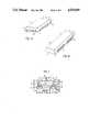
- FIG. 1A and FIG. 1Bare perspective views of examples of chip carriers, respectively, to which the present invention is applied;
- FIGS. 2A to 2Eare cross-sectional views showing a first embodiment of the present invention in sequence.
- FIG. 3is cross-sectional view showing a second embodiment of the present invention.
- each of the chip carriersincludes an enclosure 11 made of a plastic or ceramic material, in which are IC chip is hearmetically housed, and a plurality of J-shaped leads 14.
- the enclosure 11has an upper surface 1, a bottom 2 and four lateral sides 3, 4, 5 and 6.
- FIG. 1Ashows a 14-pin IC in which five leads 14 are led out from longer lateral sides 3 and 5 and four leads 14 are led out from shorter lateral sides 4 and 6.
- the four lateral sidesmay have the same length and the same number of the J-shaped leads may be extended therefrom.
- the number of the leads at each lateral sidemay be 17 for a 68-pin IC and 21 for as 84-pin chip carrier.
- the 20-pin chip carrierthe so-called SOJ IC
- FIG. 1Bhas ten leads 14 are led out from the longer sides 3 and 5 and no leads from the shorter sides 4 and 6.
- the 20 leadsare grouped into four groups having five leads, as shown.
- All the leads 14are led out of the lateral sides of the enclosure 11 laterally, bent downwards, and curled toward the bottom 2 of the enclosure. The end of the leads 14 faces the bottom 2.
- FIGS. 2A to 2Eprocess steps in the first embodiment of the invention will be described.
- the chip carrier shownfor example, in FIG. 1B with the completed J-leads is removed from the apparatus seen in FIG. 2E.
- the enclosure 11is held such that the upper surface 1 and bottom 2 are horizontally kept, and in FIG. 2A, the leads 14 are horizontally extended from the lateral sides of the enclosure 11. Moreover, to avoid complexity, the inside of the enclosure 11 is not shown.
- an IC chip(not shown) is placed in the enclosure 11 and its electrodes are electrically connected to the inner ends of the leads 14. Further, a plurality of leads to be formed are provided as shown in FIG. 1, and two of leads are shown in FIG. 2. However, the following explanation is made on one lead.
- a first process stepis conducted by use of tools and equipment shown in FIG. 2A.
- a pad 13 and a die 12are installed above and below the enclosure 11, respectively, with small clearances from the upper surface 1 and the bottom 2, respectively, and the leads 14 extending horizontally from the lateral sides 3 and 5 of the enclosure 11 are clamped by the pad 13 and die 12.
- a cutting punch 15is vertically fallen in the direction as shown by arrow 40, and the leads 14 are cutted to have a predetermined length.
- the ICis sent to the next stage shown in FIG. 2B, where a second step is conducted.
- the root 44 of the leads 14is first supported by a lower die 17.
- the leads 14are lifted, as explained later, upwards by a lead forming die 18 which contacts the lower face of the leads 14 except its root 44 and end portion 51 adjacent to the end 50 of the lead.
- the lead forming die 18has the sloped top surface and the rounded end 52.
- a punch 16is vertically fallen on the upper face of the leads.
- the punch 16has a horizontal surface portion to contact to the root 44 of the lends and a sloped surface portion above the lead forming die 18.
- the enclosure 11 with the leads having the curled end portionis sent to the next stage shown in FIG. 2C and a third step is conducted.
- the root 44 of the lead 44is clamped at a horizontal position by a pad 22 and a die 21.
- the die 21has a horizontal surface portion to clamp the root 44 of the lead and a downwardly sloped surface portion.
- a punch 24 having a downwardly sloped bottomis vertically fallen as shown by an arrow 43 to bend the leads 14 downwards at an angle of the sloped surfaces.
- the enclosure 11is placed on a die 25 with the bottom 2 contacted to the top of the die 25.
- a roller 27With the root 44 of the leads 14 is supported at its upper face by a pad 26, a roller 27 is vertically fallen as shown by an arrow 46 to bend vertically the leads 14. Thus, a vertical portion of the leads 14 between the root portion 44 and the end portion 51 is shaped.
- the roller 27can be freely rotated with the axis 27' when the roller is contacted to the lead 14.
- the axis 27'is supported by a well known bearing means (not shown) which is installed in a moving member (not shown). The roller 27 moves vertically by the moving member.
- a curling die 28has a flat top surface and a pair of curled top edges 55 of about one quarter arc of a circle (90 degrees circular arc).
- the vertical portion of the leadsis supported by a side die 48 which has a concavity 49 at its lower inside wall where a roller 31 is placed.
- the curling die 28 and the side die 48may be made of a single body, or may be set separately. In either case, a vacuum chamber is constituted at least by use of these dies 28 and 48.
- the vacuum chamberhas a hollow or opening portion 56 through which air is exhausted together with wastes and in which the roller 31 is installed.
- a curling punch 32is contacted to the upper surface 1 of the plastic enclosure 11 and to the root 44 of the leads 14, and applies thereto a pressure as shown by an arrow 47.
- the circular arc end portion 51 of the leads 14is pressed to the roller 31 and further curled gradually toward the curled top edge 55 with the rotation 29 of the roller 31.
- the end portion 51 but a part of the vertical portion of the leads 14are curled and the end 50 of the leads 14 moves along the surface of the curled edge 55 of the curling die 28 and faces the bottom 2 of the enclosure 11.
- the J-leads with a half circleare shaped.
- the curling workis easily conducted because the end portion 51 of the leads 14 has been shaped to have the circular arc beforehand.
- the leads 14do not have the curled end portion 51, the leads 14 would not be curled by the roller 31 but go straight. Further, the wastes and foreign substances produced in the curling step can be effectively exhausted to the outside through the opening 56 by the absorbing force of the vacuum and the rotation 29 of the roller 31.
- the roller 31is freely rotated with the axis 31' when contacted to the leads 14.
- the axis 31'is held by a well known bearing means (not shown) which is installed in a support member (not shown).
- the rollers 31 in the fifth stepdo not more vertically.
- the second embodimentis shown.
- the first to fourth process stepsare the same as the first embodiment shown in the FIGS. 2A to 2D.
- the final curling stepis modified from the method shown in FIG. 2E of the first embodiment to a method shown in FIG. 3.
- FIG. 3the same components as those in FIG. 2E are indicated by the same reference numerals.
- a pair of rollers 131 and 132are provided at an opening 130 which is broader than the opening 56 in the first embodiment, and the wastes produced in the curling process step are rejected from the opening 130 as the first embodiment.
- the lead 14is curled by the rollers 131 and 132 and guided to a small curled edge 135 of the curling die 128.
- curlingis conducted by the pair of rollers 131 and 132, and the curled edge 135 is used as a guide to lead the end of the leads 14 toward the bottom of the enclosure 11.
- the rollers 131 and 132are rotated as shown by arrows 29 with respective exes 131', 132' by the action from the leads contacting the rollers.
- the leadis at first contacted to the roller 131 and, after curled to some extend by the roller 131, contacted to the roller 132.
- the axes 131', 132'are supported by a well known bearing means (not shown) which is installed in a support member (not shown) and prevents vertical movement of the rollers 131 and 132.
- the plated surface of the leads 14is more hardly shaved because the leads are only contacted to a small area of the edge 135.
- the plated surface of the leadsis hardly shaved or torn, and therefore, the adhering of the wastes to the tools and equipment becomes extremely small. Consequently, cleaning of the tools and equipment can be done only after every 50,000 chip carrier's are subjected to the J-lead shaping. On the other hand, in the prior art, cleaning must be done after evey 2,000 chip carrier's are processed. Further, a short-circuiting phenomenon between leads is eliminated because the unfavorable attachment of the shaved plated surface to the curling tools can be avoided. Moreover, the occurrence of the attachment of the plastic wastes to the leads becomes zero according to the present invention.
- the chip carrier by the present inventioncan be securely soldered to a printed circuit board with a good expansion of the solder over the lead surface. Any working to remove the attached plastic wastes from the leads is not necessary.
- the present inventioneffects enables the use of the tools in highly efficiency because of decreasing the cleaning times. Moreover, a high quality and low cost product can be obtained by an enhanced automation in the product line because the attachment of the wastes to the leads in the curling step are prevented.
Landscapes
- Engineering & Computer Science (AREA)
- Manufacturing & Machinery (AREA)
- Microelectronics & Electronic Packaging (AREA)
- Lead Frames For Integrated Circuits (AREA)
Abstract
Description
Claims (7)
Priority Applications (1)
| Application Number | Priority Date | Filing Date | Title |
|---|---|---|---|
| US07/187,148US4829669A (en) | 1988-04-28 | 1988-04-28 | Method of manufacturing a chip carrier |
Applications Claiming Priority (1)
| Application Number | Priority Date | Filing Date | Title |
|---|---|---|---|
| US07/187,148US4829669A (en) | 1988-04-28 | 1988-04-28 | Method of manufacturing a chip carrier |
Publications (1)
| Publication Number | Publication Date |
|---|---|
| US4829669Atrue US4829669A (en) | 1989-05-16 |
Family
ID=22687790
Family Applications (1)
| Application Number | Title | Priority Date | Filing Date |
|---|---|---|---|
| US07/187,148Expired - LifetimeUS4829669A (en) | 1988-04-28 | 1988-04-28 | Method of manufacturing a chip carrier |
Country Status (1)
| Country | Link |
|---|---|
| US (1) | US4829669A (en) |
Cited By (12)
| Publication number | Priority date | Publication date | Assignee | Title |
|---|---|---|---|---|
| US5065504A (en)* | 1990-11-05 | 1991-11-19 | Microelectronics And Computer Technology Corporation | Method of forming flexible metal leads on integrated circuits |
| US5127447A (en)* | 1990-04-25 | 1992-07-07 | Kabushiki Kaisha Toshiba | Method of bending outer leads of a semiconductor device |
| US5135034A (en)* | 1990-02-28 | 1992-08-04 | Kabushiki Kaisha Toshiba | Outer lead forming apparatus for semiconductor device |
| US5210936A (en)* | 1992-01-06 | 1993-05-18 | Microelectronics And Computer Technology Corporation | Method and apparatus for the excise and lead form of TAB devices |
| US5375320A (en)* | 1991-08-13 | 1994-12-27 | Micron Technology, Inc. | Method of forming "J" leads on a semiconductor device |
| US5431197A (en)* | 1993-04-16 | 1995-07-11 | American Tech Manufacturing Corporation | SOJ reforming and reconditioning method and apparatus |
| US5826628A (en)* | 1996-01-24 | 1998-10-27 | Micron Technology, Inc. | Form tooling and method of forming semiconductor package leads |
| US6085804A (en)* | 1998-01-15 | 2000-07-11 | Samsung Electronics Co., Ltd. | Apparatus and method for forming leads and removing tin dust from leads |
| US20010011472A1 (en)* | 1999-12-02 | 2001-08-09 | Keiichi Sato | Manufacturing method of electronic component, manufacturing apparatus thereof, and driving method of manufacturing apparatus thereof |
| US20020117231A1 (en)* | 2001-02-26 | 2002-08-29 | Talavera Ivan G. | Device and method for shaping terminal leads |
| US20060021669A1 (en)* | 2004-07-29 | 2006-02-02 | Stark Michael R | Device for reforming socket contacts |
| US20080292743A1 (en)* | 2007-05-21 | 2008-11-27 | Semiconductor Manufacturing International (Shanghai) Corporation | Shaping die for chip package leads |
Citations (10)
| Publication number | Priority date | Publication date | Assignee | Title |
|---|---|---|---|---|
| US3416348A (en)* | 1966-09-30 | 1968-12-17 | Westinghouse Electric Corp | Flat-pack lead bending device |
| US4195193A (en)* | 1979-02-23 | 1980-03-25 | Amp Incorporated | Lead frame and chip carrier housing |
| US4463217A (en)* | 1981-09-14 | 1984-07-31 | Texas Instruments Incorporated | Plastic surface mounted high pinout integrated circuit package |
| US4465898A (en)* | 1981-07-27 | 1984-08-14 | Texas Instruments Incorporated | Carrier for integrated circuit |
| US4495376A (en)* | 1981-07-27 | 1985-01-22 | Texas Instruments Incorporated | Carrier for integrated circuit |
| US4553420A (en)* | 1983-09-30 | 1985-11-19 | Asm Fico Tooling, B.V. | Method and apparatus for touch-free lead bending |
| US4611398A (en)* | 1984-10-09 | 1986-09-16 | Gte Products Corporation | Integrated circuit package |
| JPS61236146A (en)* | 1985-04-12 | 1986-10-21 | Hitachi Ltd | Lead molding machine |
| US4698660A (en)* | 1982-03-30 | 1987-10-06 | Fujitsu Limited | Resin-molded semiconductor device |
| JPH06169758A (en)* | 1990-10-09 | 1994-06-21 | Cosmo Sogo Kenkyusho:Kk | Microorganism and production of 5-aminolevulinic acid |
- 1988
- 1988-04-28USUS07/187,148patent/US4829669A/ennot_activeExpired - Lifetime
Patent Citations (10)
| Publication number | Priority date | Publication date | Assignee | Title |
|---|---|---|---|---|
| US3416348A (en)* | 1966-09-30 | 1968-12-17 | Westinghouse Electric Corp | Flat-pack lead bending device |
| US4195193A (en)* | 1979-02-23 | 1980-03-25 | Amp Incorporated | Lead frame and chip carrier housing |
| US4465898A (en)* | 1981-07-27 | 1984-08-14 | Texas Instruments Incorporated | Carrier for integrated circuit |
| US4495376A (en)* | 1981-07-27 | 1985-01-22 | Texas Instruments Incorporated | Carrier for integrated circuit |
| US4463217A (en)* | 1981-09-14 | 1984-07-31 | Texas Instruments Incorporated | Plastic surface mounted high pinout integrated circuit package |
| US4698660A (en)* | 1982-03-30 | 1987-10-06 | Fujitsu Limited | Resin-molded semiconductor device |
| US4553420A (en)* | 1983-09-30 | 1985-11-19 | Asm Fico Tooling, B.V. | Method and apparatus for touch-free lead bending |
| US4611398A (en)* | 1984-10-09 | 1986-09-16 | Gte Products Corporation | Integrated circuit package |
| JPS61236146A (en)* | 1985-04-12 | 1986-10-21 | Hitachi Ltd | Lead molding machine |
| JPH06169758A (en)* | 1990-10-09 | 1994-06-21 | Cosmo Sogo Kenkyusho:Kk | Microorganism and production of 5-aminolevulinic acid |
Non-Patent Citations (1)
| Title |
|---|
| IBM Tech. Discl. Bull., vol. 1, No. 4, Dec. 1958, by Vullemier, p. 28.* |
Cited By (15)
| Publication number | Priority date | Publication date | Assignee | Title |
|---|---|---|---|---|
| US5135034A (en)* | 1990-02-28 | 1992-08-04 | Kabushiki Kaisha Toshiba | Outer lead forming apparatus for semiconductor device |
| US5127447A (en)* | 1990-04-25 | 1992-07-07 | Kabushiki Kaisha Toshiba | Method of bending outer leads of a semiconductor device |
| US5065504A (en)* | 1990-11-05 | 1991-11-19 | Microelectronics And Computer Technology Corporation | Method of forming flexible metal leads on integrated circuits |
| US5375320A (en)* | 1991-08-13 | 1994-12-27 | Micron Technology, Inc. | Method of forming "J" leads on a semiconductor device |
| US5210936A (en)* | 1992-01-06 | 1993-05-18 | Microelectronics And Computer Technology Corporation | Method and apparatus for the excise and lead form of TAB devices |
| US5283946A (en)* | 1992-01-06 | 1994-02-08 | Microelectronics And Computer Technology Corporation | Method and apparatus for forming metal leads |
| US5431197A (en)* | 1993-04-16 | 1995-07-11 | American Tech Manufacturing Corporation | SOJ reforming and reconditioning method and apparatus |
| US5601123A (en)* | 1993-04-16 | 1997-02-11 | American Tech Manufacturing Corporation | SOJ reforming and reconditioning method and apparatus |
| US5826628A (en)* | 1996-01-24 | 1998-10-27 | Micron Technology, Inc. | Form tooling and method of forming semiconductor package leads |
| US6085804A (en)* | 1998-01-15 | 2000-07-11 | Samsung Electronics Co., Ltd. | Apparatus and method for forming leads and removing tin dust from leads |
| US20010011472A1 (en)* | 1999-12-02 | 2001-08-09 | Keiichi Sato | Manufacturing method of electronic component, manufacturing apparatus thereof, and driving method of manufacturing apparatus thereof |
| US20020117231A1 (en)* | 2001-02-26 | 2002-08-29 | Talavera Ivan G. | Device and method for shaping terminal leads |
| US20060021669A1 (en)* | 2004-07-29 | 2006-02-02 | Stark Michael R | Device for reforming socket contacts |
| US7243688B2 (en)* | 2004-07-29 | 2007-07-17 | Intel Corporation | Device for reforming socket contacts |
| US20080292743A1 (en)* | 2007-05-21 | 2008-11-27 | Semiconductor Manufacturing International (Shanghai) Corporation | Shaping die for chip package leads |
Similar Documents
| Publication | Publication Date | Title |
|---|---|---|
| US4829669A (en) | Method of manufacturing a chip carrier | |
| JP3045818B2 (en) | Lead wire cutting blade for electrical parts | |
| GB1571173A (en) | Stamped lead frame for semiconductor packages | |
| JPH06232305A (en) | Method of manufacturing lead frame | |
| US4890154A (en) | Semiconductor package profile | |
| US5521430A (en) | Semiconductor apparatus and its manufacturing method | |
| US5495780A (en) | Method for sharpening an IC lead-frame punch | |
| US4563811A (en) | Method of making a dual-in-line package | |
| US5979510A (en) | Forming tool and method | |
| US5466967A (en) | Lead frame for a multiplicity of terminals | |
| JPS6244422B2 (en) | ||
| JP2700902B2 (en) | Lead frame manufacturing method | |
| JPH0831550B2 (en) | Semiconductor cutting shaping mold | |
| JPH0966334A (en) | Method for manufacturing heat sink for semiconductor package | |
| JPH04196257A (en) | Lead formation method of semiconductor device | |
| JP2849181B2 (en) | External lead molding method for semiconductor device | |
| JP2788780B2 (en) | External lead shape correction method | |
| JP3069630B2 (en) | Lead frame for semiconductor device | |
| JP3216227B2 (en) | Bending method of outer lead of semiconductor device | |
| KR200160429Y1 (en) | Leadframe Pad Chamfer Mold | |
| JPH0444255A (en) | Manufacture of lead frame | |
| KR0123314Y1 (en) | Double forming device of semiconductor device | |
| EP4595096A1 (en) | Lead forming device for forming an electronic component lead and a method for forming an electronic component lead | |
| JPS63308359A (en) | Manufacture of lead frame | |
| JPH0837263A (en) | Lead forming method and device for semiconductor device |
Legal Events
| Date | Code | Title | Description |
|---|---|---|---|
| AS | Assignment | Owner name:NEC CORPORATION, JAPAN Free format text:ASSIGNMENT OF ASSIGNORS INTEREST.;ASSIGNOR:NAKAJIMA, HIROFUMI;REEL/FRAME:005077/0783 Effective date:19880428 | |
| STCF | Information on status: patent grant | Free format text:PATENTED CASE | |
| CC | Certificate of correction | ||
| FEPP | Fee payment procedure | Free format text:PAYOR NUMBER ASSIGNED (ORIGINAL EVENT CODE: ASPN); ENTITY STATUS OF PATENT OWNER: LARGE ENTITY | |
| FPAY | Fee payment | Year of fee payment:4 | |
| FEPP | Fee payment procedure | Free format text:PAYER NUMBER DE-ASSIGNED (ORIGINAL EVENT CODE: RMPN); ENTITY STATUS OF PATENT OWNER: LARGE ENTITY | |
| FPAY | Fee payment | Year of fee payment:8 | |
| FEPP | Fee payment procedure | Free format text:PAYER NUMBER DE-ASSIGNED (ORIGINAL EVENT CODE: RMPN); ENTITY STATUS OF PATENT OWNER: LARGE ENTITY | |
| FEPP | Fee payment procedure | Free format text:PAYOR NUMBER ASSIGNED (ORIGINAL EVENT CODE: ASPN); ENTITY STATUS OF PATENT OWNER: LARGE ENTITY | |
| FPAY | Fee payment | Year of fee payment:12 | |
| AS | Assignment | Owner name:NEC ELECTRONICS CORPORATION, JAPAN Free format text:ASSIGNMENT OF ASSIGNORS INTEREST;ASSIGNOR:NEC CORPORATION;REEL/FRAME:013758/0440 Effective date:20021101 |