US4828224A - Chemical vapor deposition system - Google Patents
Chemical vapor deposition systemDownload PDFInfo
- Publication number
- US4828224A US4828224AUS07/108,771US10877187AUS4828224AUS 4828224 AUS4828224 AUS 4828224AUS 10877187 AUS10877187 AUS 10877187AUS 4828224 AUS4828224 AUS 4828224A
- Authority
- US
- United States
- Prior art keywords
- sub
- substrates
- substrate
- housing
- reaction chamber
- Prior art date
- Legal status (The legal status is an assumption and is not a legal conclusion. Google has not performed a legal analysis and makes no representation as to the accuracy of the status listed.)
- Expired - Lifetime
Links
- 238000005229chemical vapour depositionMethods0.000titledescription33
- 238000002955isolationMethods0.000claimsabstractdescription28
- 238000007789sealingMethods0.000claimsdescription4
- 230000001154acute effectEffects0.000claimsdescription2
- 239000000758substrateSubstances0.000abstractdescription146
- 238000012545processingMethods0.000abstractdescription56
- 238000006243chemical reactionMethods0.000abstractdescription50
- 238000010438heat treatmentMethods0.000abstractdescription19
- 239000000463materialSubstances0.000abstractdescription19
- 239000000376reactantSubstances0.000abstractdescription17
- 238000000151depositionMethods0.000abstractdescription14
- 238000011109contaminationMethods0.000abstractdescription12
- 238000012935AveragingMethods0.000abstractdescription9
- 238000004519manufacturing processMethods0.000abstractdescription8
- 239000004065semiconductorSubstances0.000abstractdescription7
- 238000000605extractionMethods0.000abstractdescription3
- 238000002347injectionMethods0.000abstractdescription2
- 239000007924injectionSubstances0.000abstractdescription2
- 230000007246mechanismEffects0.000description26
- 238000000034methodMethods0.000description14
- 238000010926purgeMethods0.000description14
- 230000003028elevating effectEffects0.000description11
- 230000008021depositionEffects0.000description9
- 230000008569processEffects0.000description8
- 238000005137deposition processMethods0.000description5
- 239000000356contaminantSubstances0.000description4
- 230000007613environmental effectEffects0.000description4
- 238000003780insertionMethods0.000description3
- 230000037431insertionEffects0.000description3
- 235000012431wafersNutrition0.000description3
- 238000000429assemblyMethods0.000description2
- 238000012986modificationMethods0.000description2
- 230000004048modificationEffects0.000description2
- 230000003287optical effectEffects0.000description2
- 239000011435rockSubstances0.000description2
- 230000000712assemblyEffects0.000description1
- 230000008859changeEffects0.000description1
- 150000001875compoundsChemical class0.000description1
- 230000008878couplingEffects0.000description1
- 238000010168coupling processMethods0.000description1
- 238000005859coupling reactionMethods0.000description1
- 238000000354decomposition reactionMethods0.000description1
- 230000003247decreasing effectEffects0.000description1
- 230000000694effectsEffects0.000description1
- 230000001939inductive effectEffects0.000description1
- 239000002245particleSubstances0.000description1
- 239000010453quartzSubstances0.000description1
- VYPSYNLAJGMNEJ-UHFFFAOYSA-Nsilicon dioxideInorganic materialsO=[Si]=OVYPSYNLAJGMNEJ-UHFFFAOYSA-N0.000description1
- 238000004347surface barrierMethods0.000description1
Images


Classifications
- C—CHEMISTRY; METALLURGY
- C30—CRYSTAL GROWTH
- C30B—SINGLE-CRYSTAL GROWTH; UNIDIRECTIONAL SOLIDIFICATION OF EUTECTIC MATERIAL OR UNIDIRECTIONAL DEMIXING OF EUTECTOID MATERIAL; REFINING BY ZONE-MELTING OF MATERIAL; PRODUCTION OF A HOMOGENEOUS POLYCRYSTALLINE MATERIAL WITH DEFINED STRUCTURE; SINGLE CRYSTALS OR HOMOGENEOUS POLYCRYSTALLINE MATERIAL WITH DEFINED STRUCTURE; AFTER-TREATMENT OF SINGLE CRYSTALS OR A HOMOGENEOUS POLYCRYSTALLINE MATERIAL WITH DEFINED STRUCTURE; APPARATUS THEREFOR
- C30B29/00—Single crystals or homogeneous polycrystalline material with defined structure characterised by the material or by their shape
- C30B29/02—Elements
- C30B29/06—Silicon
- C—CHEMISTRY; METALLURGY
- C30—CRYSTAL GROWTH
- C30B—SINGLE-CRYSTAL GROWTH; UNIDIRECTIONAL SOLIDIFICATION OF EUTECTIC MATERIAL OR UNIDIRECTIONAL DEMIXING OF EUTECTOID MATERIAL; REFINING BY ZONE-MELTING OF MATERIAL; PRODUCTION OF A HOMOGENEOUS POLYCRYSTALLINE MATERIAL WITH DEFINED STRUCTURE; SINGLE CRYSTALS OR HOMOGENEOUS POLYCRYSTALLINE MATERIAL WITH DEFINED STRUCTURE; AFTER-TREATMENT OF SINGLE CRYSTALS OR A HOMOGENEOUS POLYCRYSTALLINE MATERIAL WITH DEFINED STRUCTURE; APPARATUS THEREFOR
- C30B25/00—Single-crystal growth by chemical reaction of reactive gases, e.g. chemical vapour-deposition growth
- C30B25/02—Epitaxial-layer growth
- C30B25/10—Heating of the reaction chamber or the substrate
- Y—GENERAL TAGGING OF NEW TECHNOLOGICAL DEVELOPMENTS; GENERAL TAGGING OF CROSS-SECTIONAL TECHNOLOGIES SPANNING OVER SEVERAL SECTIONS OF THE IPC; TECHNICAL SUBJECTS COVERED BY FORMER USPC CROSS-REFERENCE ART COLLECTIONS [XRACs] AND DIGESTS
- Y10—TECHNICAL SUBJECTS COVERED BY FORMER USPC
- Y10S—TECHNICAL SUBJECTS COVERED BY FORMER USPC CROSS-REFERENCE ART COLLECTIONS [XRACs] AND DIGESTS
- Y10S414/00—Material or article handling
- Y10S414/135—Associated with semiconductor wafer handling
- Y10S414/137—Associated with semiconductor wafer handling including means for charging or discharging wafer cassette
- Y—GENERAL TAGGING OF NEW TECHNOLOGICAL DEVELOPMENTS; GENERAL TAGGING OF CROSS-SECTIONAL TECHNOLOGIES SPANNING OVER SEVERAL SECTIONS OF THE IPC; TECHNICAL SUBJECTS COVERED BY FORMER USPC CROSS-REFERENCE ART COLLECTIONS [XRACs] AND DIGESTS
- Y10—TECHNICAL SUBJECTS COVERED BY FORMER USPC
- Y10S—TECHNICAL SUBJECTS COVERED BY FORMER USPC CROSS-REFERENCE ART COLLECTIONS [XRACs] AND DIGESTS
- Y10S414/00—Material or article handling
- Y10S414/135—Associated with semiconductor wafer handling
- Y10S414/139—Associated with semiconductor wafer handling including wafer charging or discharging means for vacuum chamber
Definitions
- This inventionrelates in general to systems for chemical vapor deposition of materials on substrates, and more particularly to a chemical vapor deposition system having improved substrate loading, off-loading, and handling sub-systems which interact with at least one especially configured processing subsystem having a reaction chamber, susceptor and heating sub-assemblies for precision control of the deposition process.
- Chemical vapor deposition processesincludes passing of a reactant gas, which contains the material to be deposited, over the substrates for forming, or growing a compound on the substrates as a result of thermal reaction or decomposition of the various gaseous materials.
- the equipment used to accomplish such a processis of various configurations but will include the basic components of a reaction chamber, a heating system and a gas flow system. Of course these various components are configured in accordance with the tasks to be accomplished. For example, when the number of substrates to be processed is small, the reaction chamber may be in the form of a bell jar, but in high quantity production work considerably more sophisticated equipment is needed.
- a horizontal gas flow systemgenerally includes a platform, or susceptor as it is referred to in the art, which is located in a horizontally disposed reaction chamber with the reactant gas flowing in a horizontal path across the susceptor.
- a horizontally disposed susceptor, or an upstanding multi-surface barrier shaped susceptoris located in a vertically disposed reaction chamber with the reactant gas being caused to flow in a substantially vertical path past and around the susceptor.
- these susceptorsare configured to support a multiplicity of relatively small substrates, i.e. in the neighborhood of 2 to 5 inches in diameter, for simultaneously depositing materials on the multiplicity of substrates. While simultaneous deposition of materials on a multiplicity of substrates is desirable from a manufacturing standpoint, it has some drawbacks from a quality standpoint.
- the cassette elevatorwhich is identified as Product No. 6200, includes a vacuum chamber for receiving a plurality of substrates that are carried in a cassette with the cassette being supported on a platform.
- the platformis vertically movable by means of an elevating mechanism which brings the substrates one at a time into alignment with an access port.
- An isolation valvesuch as that available as Product No.
- the Brooks Automation Co.also markets a vacuum transport station under the name Vacu-TranTM for extracting the substrates one at a time from the elevating mechanism described above.
- the transport stationincludes a housing which is coupled to the isolation valve described above, and a robot arm structure is located in the housing.
- the robot arm structureincludes a rotatable plate having an extensible and retractable arm arrangement thereon, with a pallet or spatula on the distal end of the arms. With the plate and arms rotated so as to align with the access port of the elevating mechanism and the isolation valve open, the arms are extended to move the pallet into position below a substrate, and then the entire arm structure is raised to lift the substrate so that it is carried on the pallet out of the cassette.
- the armsare then retracted to extract the substrate from the elevating mechanism, and then the arm assembly is rotated to another position and extended once again so as to pass through another isolation valve into a suitable reaction chamber.
- This particular handling systemrelies on the weight of the substrate to hold it in place on the pallet and another prior art structure includes a similar arm arrangement which further includes a vacuum outlet on the pallet for a more positive attachment to the underside of the substrates.
- the reaction chambers used in single substrate processing systemsmay be categorized as either a horizontal gas flow system or a vertical gas flow system.
- the susceptors being used in the single substrate reaction chambersconsist essentially of a planar platform or base upon which the substrate rests during the deposition process, and those susceptors contribute nothing further to the deposition process with regard to improving the problems of depletion of the material carried by the reactant gas as it flows past and around the substrate, and with regard to improved temperature sensing and control.
- a new and improved chemical vapor deposition systemfor depositing various materials on substrates as part of the process for manufacturing semiconductor devices.
- the present systemis broadly categorized as a horizontal gas flow system in that the reactant gas which carries the materials to be deposited, is directed in a horizontal flow path through the reaction chamber in which the substrates are processed.
- the systemis further categorized as a single substrate processing system as opposed to a batch processing system, in that one relatively large substrate is processed per cycle of the system.
- the system of the present inventionis configured so that a plurality of independent single substrate processing cycles can be simultaneously accomplished.
- the chemical vapor deposition system of the present inventionincludes the following major sub-systems.
- a special substrate loading sub-systemis provided for receiving cassettes which carry a multiplicity of substrates to be processed, and an identical off-loading sub-system is provided for receiving processed substrates that are to be removed in cassettes from the system.
- Both the loading and off-loading sub-systemsinclude a unique built-in isolation valve which closes off the rest of the system from environment contamination whenever these sub-systems are opened for insertion for removal of the cassettes.
- a special substrate handling sub-systemas fully disclosed in the Assignee's Copending Application Ser. No. 048,630, filed May 11, 1987, entitled WAFER HANDLING SYSTEM WITH BERNOULLI PICK-UP, which is hereby expressly incorporated herein by reference, includes a housing having a loading port to which the substrate loading sub-system is coupled and an unloading port to which the off-loading sub-system is coupled.
- a special robot arm assemblyis mounted in the housing for rotary and extensible movements for substrate handling purposes.
- a pick-up wandis mounted on the distal end of the robot arms for positioning above the substrates to be handled, and a special gas flow arrangement is provided in the robot arm assembly so that the pick-up wand operates in accordance with Bernoulli's principle for moving the substrates within the system without any mechanical contact being made with the top or bottom planar surfaces of the substrates.
- the housing of the substrate handling sub-systemis provided with a delivery port through which substrates are supplied to and retrieved from a processing sub-system which is coupled to the delivery port.
- the housingmay be provided with a plurality of such delivery ports to which an equal number of processing sub-systems are coupled.
- a special isolation valve assembly having a ported gate valveis mounted proximate delivery port of the housing for closing that delivery port whenever a chemical vapor deposition cycle is being accomplished in the processing sub-system.
- a gas injection structureas fully disclosed in the Assignee's Copending Application Ser. No. 066,019, filed June 24, 1987, entitled IMPROVED GAS INJECTORS FOR REACTION CHAMBERS IN CVD SYSTEMS, and in Copending Application Ser. No. 063,409, Filed June 18, 1987, entitled HEATING SYSTEM FOR REACTION CHAMBER FOR CVD EQUIPMENT, both of which are hereby expressly incorporated herein by reference, is interposed between the isolation valve assembly and the inlet of the processing sub-system.
- the gas injectoris configured to provide a reactant gas flow of special character through the reaction chamber.
- the processing sub-system in which the chemical vapor deposition process takes placeincludes a reaction chamber which is fully disclosed in the Assignee's Copending Application Ser. No. 065,945, filed June 24, 1987, entitled IMPROVED REACTION CHAMBER FOR CVD SYSTEMS, which is hereby expressly incorporated herein by reference.
- the reaction chamberis especially configured to provide desirable gas flow characteristics for accomplishing the deposition process in a precisely controllable environment.
- the reaction chamber housingis also configured for mounting of a special substrate supporting mechanism with temperature sensing devices therein.
- This sub-systemis designed for optimum temperature averaging and control, and for reactant gas flow averaging, and includes a circular susceptor for supporting a single substrate, with the susceptor being disposed within the reaction chamber on a driveshaft assembly which axially depends from the susceptor through a depending tubular shaft of the reaction chamber housing.
- the driveshaft assemblyis rotatably drivable for rotation of the susceptor and thus the single substrate supportable thereon.
- the critical temperatures at various points of the susceptorare sensed by a special temperature sensing arrangement which includes a master temperature sensor that is located in the vicinity of the center of the susceptor.
- a special fixed ringis located in concentric relationship with the rotatable susceptor, and plurality of, slave temperature sensors are located in the fixed ring for sensing the temperature at various points near the periphery of the susceptor.
- the master and slave temperature sensorsproduce signals indicative of the temperatures sensed thereby, and the signals are transmitted to a suitable temperature control means.
- the processing sub-system of the chemical vapor deposition system of this inventionfurther includes a heating system that is fully disclosed in the Assignee's Copending Application Ser. No. 063,409, filed June 18, 1987, entitled HEATING SYSTEM FOR REACTION CHAMBER OF CHEMICAL VAPOR DEPOSITION EQUIPMENT, that is hereby expressly incorporated herein by reference.
- the heating systemincludes an upper radiant heat assembly which is disposed atop the reaction chamber for directing radiant heat downwardly into the chamber a lower radiant heat assembly is located below the reaction chamber for directing heat upwardly into the chamber.
- a heat concentrator structurewhich is part of the lower heating assembly, is provided for directing concentrated radiant heat into the vicinity of the center of the susceptor where the master temperature sensor is located, with the heat concentrator providing optimum temperature control.
- the upper and lower heating structureshave individually controllable banks of discrete heating elements for precision heat control of the various regions in and about the rotatable susceptor.
- system of the present inventionis provided with various purging sub-systems for controlling the gas flow within the system and maintaining a contaminant free environment therein.
- Another object of the present inventionis to provide a new and improved chemical vapor deposition system which includes special substrate loading and unloading sub-systems wherein cassettes containing multiplicities of substrates are inserted into the system for processing and retrieved from the system subsequent to processing with the loading and unloading sub-systems eliminating, or at least substantially reducing, system contamination resulting from the insertion and retrieval of the cassettes.
- Another object of the present inventionis to provide a new and improved chemical vapor deposition system having a special substrate handling system including a special robot arm structure which moves the substrates in the system without coming into physical contact with the top and bottom planar surfaces of the substrates.
- Another object of the present inventionis to provide a new and improved chemical vapor deposition system of the above described character wherein the substrate handling sub-system is operable for moving individual substrates from the loading sub-system into a desired one of the plurality of processing sub-systems for processing and retrieving the substrates after processing and delivering the processed substrates to the unloading sub-system.
- Another object of the present inventionis to provide a chemical vapor deposition system which includes ported gate valves which isolates the substrate handling sub-system from the processing sub-system at all times except when substrates are being inserted into or retrieved from the processing sub-systems.
- Another object of the present inventionis to provide a new and improved chemical vapor deposition system which further includes special gas injectors for inducing special flow characteristics in the gas that is supplied to the processing sub-systems.
- Another object of the present inventionis to provide each of the processing sub-systems of the system with a reaction chamber housing that induces desired gas flow characteristics through the reaction chamber and is configured to accommodate a special susceptor and heat sensing sub-system.
- Another object of the present inventionis to provide a new and improved chemical vapor deposition system of the above described character wherein a circular susceptor is mounted in the reaction chamber for supporting a single substrate, with the susceptor being rotatably driven to rotate the substrate about an axis which is normal with respect to the center thereof for optimum averaging of temperature differences and material concentration differences in the reactant gas to eliminate, or at least substantially reduce, the undesirable effects of those variables on the deposition process.
- Another object of the present inventionis to provide a new and improved chemical vapor deposition system wherein a special temperature sensing arrangement is provided to sense the temperatures in and about the rotatable susceptor and producing signals which are used for controlling the heat input to the various regions in and about the susceptor.
- Another object of the present inventionis to provide a new and improved chemical vapor deposition system of the above described character which further includes a special heating sub-system which is controllable to direct variable amounts of radiant heat energy into the reaction chamber for optimized heating of the various regions in and about the rotatable susceptor.
- Another object of the present inventionis to provide a new and improved chemical vapor deposition system of the above described type wherein purging sub-systems are provided at various points in the system for controlling gas flow within the system and for maintaining a contaminant free environment within the system.
- Still another object of the present inventionis to provide a new and improved mechanism for loading various articles into a processing system, or retrieving various articles from a processing system, with the mechanism including a built-in isolation valve which prevents environmental contamination of the processing system.
- Yet another object of the present inventionis to provide a new and improved isolation valve for use between various sub-systems of a processing system for selective isolation of the sub-systems.
- FIG. 1is a perspective view of the chemical vapor deposition system of the present invention which shows some of the various features thereof.
- FIG. 2is an enlarged fragmentary sectional view taken along the line 2--2 of FIG. 1.
- FIG. 3is an enlarged fragmentary sectional view taken along the line 3--3 of FIG. 1.
- FIG. 4is a fragmentary sectional view taken along the line 4--4 of FIG. 3.
- FIG. 5is a fragmentary sectional view taken along the line 5--5 of FIG. 3.
- FIG. 6is a fragmentary sectional view taken along the line 6--6 of FIG. 1.
- FIG. 7is an enlarged fragmentary sectional view taken along the line 7--7 of FIG. 6.
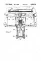
- FIG. 8is a schematic plan view of the system of the present invention which is partially broken away to show the various relationships and features of the sub-systems and components thereof.
- FIGS. 1 and 8best show the chemical vapor deposition system of the present invention which is indicated in its entirety by the reference numeral 10.
- the system 10is formed of several sub-systems which includes a substrate loading sub-system 12, an identical substrate unloading sub-system 14, a substrate handling sub-system 16.
- three identical processing sub-systems 18are shown, but it will be understood that the deposition system 10 is completely operational with a single processing sub-system 18, and additional processing sub-systems 18 are employed, if desired, for production purposes.
- the loading and unloading sub-systems 12 and 14 respectivelyare identical with the difference being in the way that they are operated. Since the sub-systems 12 and 14 are identical, it will be understood that the following detailed description of the loading sub-system 12 will also apply to the unloading sub-system 14.
- the substrate loading sub-system 12includes an upper housing 20 which defines a hermetically sealable cassette receiving interior chamber 22.
- the upper housing 20has a hatch 24 which is hingedly mounted on the housing 20 with a suitable latch 25 being provided for opening the hatch so that a cassette 26, which is shown in dashed lines in FIG. 2, may be placed in and retrieved from the interior cassette receiving chamber 22.
- the cassette 26, as is well known in the art,is a case-like structure having an open side 27 with a plurality of shelf-like supports (not shown) therein for containing and providing lateral access to a plurality of substrates 28 that are carried in vertically spaced stacked relationship with the cassette 26.
- the upper housing 20includes a floor 29 having a large central opening 30 formed therethrough with that opening being closed by a cassette support platform 32 whenever a cassette 26 is being loaded into or unloaded from the receiving chamber 22, as will hereinafter be described.
- the loading sub-system 12further includes an intermediate housing 34 which is bolted or otherwise attached so as to be immediately below the upper housing 20, and is configured to define an interior feed chamber 36.
- the intermediate housing 34is open at its top end so that the floor 29 of the upper housing 20 forms the top wall of the intermediate housing 34, with the central opening 30 of the floor 29 being located so as to open into the feed chamber 36.
- the intermediate housing 34further includes a sidewall 38 having a lateral feed port 40 formed therein, and a bottom wall 42 which is provided with a central opening 44 that is in axial alignment with the central opening 30 of the upper housing 20.
- the cassette support platform 32is mounted on the upper end of an elevator shaft 46 for vertical movement between an elevated position shown in solid lines in FIG. 2, and a fully lowered position shown in phantom lines in the same figure.
- the support platform 32has a seal means 48 such as an O-ring mounted thereon to extend upwardly from its top surface 49. Therefore, when the support platform 32 is fully elevated, the seal means 48 engages the lower surface of the floor 29 about the central opening 30 thereof so that the receiving chamber 22 of the upper housing 20 is hermetically sealed from the feed chamber 36 of the intermediate housing 34 when the cassette support platform 32 is in the elevated position.
- the floor 29 with its central opening 30 and the vertically movable cassette support platform 32cooperate to provide the loading sub-system 12 with a built-in isolation valve which isolates the feed chamber 36 of the intermediate housing 34 from the cassette receiving chamber 22 of the upper housing 20.
- isolationis provided so that whenever the hatch 24 is opened for loading or retrieval of a cassette 26, environmental contamination will be kept out of the feed chamber 36 of the intermediate housing 34 and thus out of the rest of the system 10 as will become apparent as this description progresses.
- the upper housing 20is provided with a purge gas inlet port 50 in its top wall 51 and a purge gas outlet port 52 in one of its sidewalls 53.
- the purge gas outlet port 52is coupled to a suitable gas disposal location (not shown) by an exhaust tube 54 which is welded or otherwise fixedly attached to a mounting plate 55 that is bolted to the housing 20 and has a suitable O-ring seal 56.
- the purge gas inlet port 50is similarly coupled to a remote source of pressurized purge gas (not shown) by a supply tube 57 with a similar mounting plate 58.
- an elevator means 60in mounted below the intermediate housing 34 with the above mentioned elevator shaft 46 extending therefrom so as to pass axially through the opening 44 provided in the bottom wall 42 of the intermediate housing 34.
- the top end of the elevator shaft 46is axially disposed in a bellows seal assembly 62 of the type well known in the art.
- the bellows seal assembly 62includes an axially extensible bellows 64 having an upper mounting plate 65 which is attached to the lower surface of the cassette support platform 32 and a lower mounting plate 66 which is attached in the manner shown to the bottom wall 42 of the intermediate housing 34. In this manner, the feed chamber 36 is isolated from the elevator means 60 to prevent any contamination from entering the feed chamber 36 from the elevator means 60.
- the elevator means 60includes an elongated housing 68 that is bolted or otherwise attached so as to be supported and depend from the intermediate housing 34, with the housing 68 defining an internal chamber 70.
- An elongated guide rail 72is mounted within the elevator housing 68 with a pair of tracks 74 being formed on its opposed longitudinal edges, and an elevator carriage 76 is mounted for vertical reciprocal movement on the guide rail.
- the carriage 76includes a housing 78 with suitable wheels 79 mounted thereon which engage the tracks 74 of the guide rail 72.
- the elevator shaft 46is fixedly carried in a bore 80 formed in the carriage such as by the illustrated set screws 81 and the elevator shaft defines an axial bore 82 with an open lower end.
- An elongated lead screw 84is journaled for rotation in a bearing assembly 86 that is suitably mounted in the bottom wall 87 of the elevator housing 68 so that the lower end 88 of the lead screw 84 depends axially from the housing 68, and the upper threaded end 90 extends axially upwardly through the bore 80 of the carriage housing 78 so as to be axially disposed in the bore 82 of the elevator shaft 46.
- a follower nut 92is bolted or otherwise affixed to the lower end of the carriage housing 78 so that it's internally threaded bore 94 is in threaded engagement with the lead screw 84.
- a plate 96is mounted on the lower surface of the bottom wall of the elevator housing 68 and the plate 96 has a laterally extending portion 97 upon which a drive motor 98 is mounted.
- the drive motor 98is an electrically and reversibly operated digital stepping motor of the type well known in the art, and has a drive pulley 100 mounted for rotation with its output shaft 102.
- a suitable drive belt 104is employed for coupling the drive pulley 100 of the motor 98 to a driven pulley 106 that is mounted fast on the depending lower end 88 of the lead screw 84.
- the lead screw 84When the drive motor 98 is operated, the lead screw 84 will be rotated about its longitudinal axis with the follower nut 92 causing the carriage 76 to move along the guide rail 72 either upwardly or downwardly as determined by the rotational direction of the drive motor 98.
- the carriage 76When the carriage 76 is in its lowered position as shown in FIG. 3, the cassette support platform 32 will be lowered, and the carriage is upwardly movable to raise the cassette support plate 32 to its upper position wherein it performs the above described isolation valve function.
- a lower limit switch 108is mounted in the elevator housing 68 for engaging a suitable switch actuator arm 110 that is mounted on the carriage housing 78.
- the lower limit switch 108is used as an emergency stopping device which prevents the carriage from moving below a desired lower limit.
- An upper limit switch 112is similarly mounted in the elevator housing 68 for contact by the same switch actuator arm 110 when the carriage 76 reaches its upper position.
- the upper limit switch 112produces a signal indicative of the up-position of the substrate support platform 32 and that signal is used by a suitable control means (not shown) to actuate a latching means 114 which is shown in FIG. 4.
- the illustrated latching mechanism 114is a commercially available power clamp that is marketed by the DE-STA-CO division of Dover Resources, Inc., 250 Park Street, Troy, MI 48007-2800.
- the latching mechanism 114which is identified as Model No. 807-L, is mounted on the exterior of the elevator housing 68 by being bolted to a mounting bracket 115 that is provided on the housing for that purpose.
- the latching mechanism 114includes a pneumatic (or hydraulic) cylinder 116 having the usual reciprocally extensible rod 117 which operates an over-center linkage 118 for moving a clamping arm 119 back and forth through an opening 120 formed in the housing 68 and an aligned opening 121 formed through the guide rail 72.
- the clamping arm 119is movable from a carriage latching position shown in solid lines in FIG. 4 to a carriage releasing position shown in dashed lines in the same figure.
- the clamping arm 119is especially configured to provide a first indicator lug 122 which interacts with a first detector switch 124, such as an optical sensor, to produce a control signal indicative of a latched position of the arm 119.
- a second indicator lug 126is also provided on the arm 119 to interact with a second detector switch 128, that is mounted on the cylinder 116 by means of a suitable bracket 130, to provide a control signal that is indicative of the unlatched position of the clamping arm 119.
- the latching mechanism 114is operable to clamp and hold the cassette support platform 32 in sealed engagement with the floor 29 of the upper housing 20 by bearing engagement of the adjustable bolt 132 that is mounted on the distal end of the clamping arm 119 with the lower end of the carriage 76, as indicated in FIG. 4.
- the power clamp 114will maintain the latched position of the arm 119 despite power failures, equipment shut-down and the like to prevent system contamination during such periods as well as during operation.
- another position indicatoris provided in the elevator means 60, and includes a mounting assembly 134 for adjustably carrying a lug 136.
- a sensor device 138such as an optical sensor, is mounted in the housing 68 so as to interact with the lug 138 to produce a control signal indicative of the alignment of the lowermost substrate 28 in the cassette 26 with the feed port 40 of the intermediate housing 34.
- the latching mechanism 114is operated to move the latching arm 119 to its unlatched position. Then, the drive motor 98 is operated in a stepping manner to lower the carriage 76 and support platform 32.
- the position indicator lug 136is aligned with the sensing switch 138, the resulting control signal is supplied to a control system (not shown) which sequentially lowers the support platform 32, and therefore the cassette 26, to sequentially move the substrates into the desired position relative to the feed port 40 of the intermediate housing 34.
- the loading sub-system 12is mounted on the substrate handling sub-system 16 which, as will hereinafter be described, is operated to extract the substrates 28 from the loading sub-system 12 for sequential processing in the system 10.
- the substrate unloading sub-system 14is similarly mounted on the handling sub-system 16 for receiving the processed substrates from the system for unloading therefore, the unloading sub-system 14 which is identical to the loading sub-system 12, is operated in a reversed manner to accomplish the processed substrate unloading operation.
- the substrate handling sub-system 16is shown as including a housing 140 which defines an internal chamber 142.
- the housing 140includes a suitable substrate input port 143 which is aligned with the feed port 40 of the substrate loading sub-system 12, and a substrate output port 144 that is aligned with the feed port 40 of the substrate unloading sub-system 14.
- the housing 140is also provided with at least one substrate delivery port 146 through which substrates to be processed are passed into the processing sub-system(s) 18.
- a special wafer handling mechanism 148having a pair of articulated robot arms 150 and 152 each having a proximal end mounted for rotational movement about drive shafts 153 and 154, respectively.
- Each of the arms 150 and 152also have an intermediate joint 156 with a special pick-up wand 158 being mounted on the distal ends of the arms.
- the arm drive shafts 153 and 154are driven in opposite rotational directions for extending and retracted folding movements of the robot arms 150 and 152 to move the pick-up wand toward and away from the uppermost end of a robot arm drive assembly 160 upon which the proximal ends of the arms are mounted and which drives the robot arms.
- the drive assembly 160includes a first drive motor 161 which rotatably drives a center shaft (not shown) that extends upwardly from the motor 161 through the center of a coaxial bearing and seal mechanism 164 and drives the internal gears (not shown) of a gear box 166 for rotational driving of the drive shafts 153 and 154.
- a second motor 170is provided which rotatably drives a tubular shaft (not shown), that is concentrically disposed about the above-described center shaft, and also extends through the mechanism 164 for rotation of the entire gear head 168.
- the gear head 168is therefore rotatable for selected positioning of the robot arms 150 and 152 in alignment with the various ports 143, 144 and 146 of the housing 140 by operation of the motor 170.
- the other drive motor 160is operated for foldingly extending and retracting the robot arms 150 and 152 to move the pick-up wand 158 to the desired locations for picking up and delivering the substrates 28.
- the pick-up wand 158operates in accordance with the Bernoulli principle to produce an area of relatively low pressure between the downwardly facing surface of the wand 158 and the upwardly facing surface of the substrate to be moved. In this manner, the pick-up wand 158 can lift and move the substrates 28 without ever touching the top or bottom planar surfaces of the substrate. The only physical contact between the wand 158 and the substrates is an edge contact which is made so that the substrates will move along with the wand.
- the pick-up wand 158is provided with a special array of gas outlet apertures (not shown) which open onto the lower surface of the pick-up wand with those apertures being coupled to a remote source of gas under pressure (not shown). The connection of the wand to a remote source of gas is made via passages formed through the robot arms 150 and 152 and downwardly through the drive assembly 160.
- the housingis provided with a purge gas inlet 172 and a purge gas outlet 174 which may be coupled to the same sources and disposal location as the drive assembly 160 and the loading and unloading sub-systems 12 and 14.
- the substrate handling sub-system 16moves the substrates to be processed through a special isolation valve 176 and gas injector 178, as seen in FIG. 6, into the processing sub-system 18. It also, of course retrieves the processed substrates by moving the back through the gas injector 178 and isolation valve 176 when processing is completed.
- the housing 140 of the substrate handling sub-system 16, as shown in FIGS. 6 and 7,is provided with an opening 179 in it's bottom surface 180 adjacent it's delivery port 146, and the isolation valve 176 is mounted in that opening so as to be disposed in the housing 140 proximate the delivery port 146.
- the isolation valve 176includes a mounting plate 182 that is bolted or otherwise attached to the bottom surface 180 of the housing 140 so as to hermetically seal the opening 179 and support the various components of the isolation valve.
- a pair of actuator support arms 184depend from the mounting plate 182 in spaced apart relationship with respect to each other, and a rock shaft 186 is transversely journaled for rotation in bushing blocks 188 that are mounted on the lower ends of the actuator support arms 184.
- valve body support arms 204are mounted so as to extend upwardly from the mounting plate 182 in spaced apart relationship with respect to each other.
- Suitable bearings 206are mounted in the top end of each of the support arms 204 for journaling of a pivot axis 208 which is mounted in the valve body 200.
- the valve body 200is of elongated configuration having opposed planar surfaces 209 and 210 with an elongated open port 212 extending transversely through the body so as to open onto both of the opposed planar surfaces 209 and 210.
- the pivot axis 208extends longitudinally through the valve body 200 proximate the side edge 214 thereof with the opposite longitudinal side edge forming a valve closing surface 216. As shown best in FIG. 6, the valve closing surface 216 is disposed to form an acute angle of approximately 30-40 degrees with respect to open port 212 thereof.
- An O-ring type sealing gasket 218is provided on the valve closing surface 216 of the valve body 200.
- the valve body 200When the actuator 190 is in it's retracted state, the valve body 200 will be in the solid line position as shown in FIG. 6, with this position being referred to as the open position of the isolation valve 176. When in this open position, the open port 212 will be disposed in parallel relationship with the mounting plate 182 so that the distal ends of the robot arms 150 and 152 and the wand 158, along with the substrates carried thereby, can be moved through the port 212 of the valve body 200. When the actuator 190 is opened to move the extensible rod 192 to its extended state, the valve body 200 will be pivotably moved through less than 90° of rotation to the closed dashed line position shown in FIG. 6, to bring the valve closing surface 216 into seated sealing engagement with the gas injector structure 178 which is adjacent thereto.
- the injector housing 220is further provided with a gas flow passage 228 that is normal with respect to the through port 222 and extends upwardly therefrom so as to open onto the top edge surface of the housing 220.
- An elongated flow control plate 230having a plurality of variously sized apertures 232 (one shown) formed in spaced increments along its length, is mounted on the top edge of the injector housing 220 so that the apertures 232 open into the gas flow passage 228 of the housing 220.
- a gas inlet body 234is mounted atop the flow control plate 230 and is configured to define a plenum chamber 36 having a bottom which opens onto the upper surface of the flow control plate.
- a gas inlet conduit 238is mounted on the top end of the inlet body 234 for supplying gas under pressure from a remote source (not shown) to the plenum chamber 236.
- the plenum chamberdistributes the gas pressure equally to all points in the chamber so that equal gas pressures will be applied to the open top end of each of the apertures 232.
- the gaswill therefore flow into the gas flow passage 228 at various velocities as determined by the apertures of the flow control plate 230.
- the gaspasses downwardly into the through port 222 with a predetermined velocity profile through the gas outlet side 227 thereof into the processing sub-system 18.
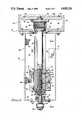
- the processing sub-system 18, as seen best in FIGS. 6 and 7,includes a reaction chamber 240 which, as hereinbefore stated, is fully disclosed in the Copending Patent Application Ser. No. 065,945 filed on June 24, 1987, and is expressly incorporated herein by reference.
- the reaction chamber 240is an especially configured horizontal flow low-profile housing designed for producing desired gas flow characteristics from it's inlet end 242 to it's outlet end 244.
- the reaction chamberis formed of a material which is transparent to radiant heat energy, such as quartz, and is configured to work in conjunction with a special substrate supporting susceptor and temperature sensing sub-system 246.
- the substrate supporting susceptor and temperature sensing sub-system 246is fully disclosed in the Copending Patent Application Ser. No. 032,474, filed on Mar. 31, 1987, which is expressly incorporated by reference. However, a brief description of the mechanism 246 will now be presented to provide a complete understanding of the system 10 of the present invention.
- the substrate supporting and temperature sensing sub-system 246includes a circular susceptor 248 which is configured to support a single substrate for rotation about an axis which is normal with respect to the center of the substrate.
- the circular susceptor 248is mounted in the reaction chamber 240 on the upper end of a driveshaft assembly 250 which axially extends from the susceptor through a tubular shaft 252 that depends from the floor of the reaction chamber 240, as shown in FIG. 6.
- the driveshaft assembly 250is coupled to a drive means 254 which rotates the driveshaft 250 and thus the susceptor 248.
- the tubular shaft 252is sealingly coupled as at 256 to the drive means 254 and a purge gas inlet conduit 258 is provided for supplying purge gas from a remote source of gas under pressure (not shown).
- the purge gasis directed into the drive means 254 and is supplied through the tubular shaft 252 of the reaction chamber 240 and the driveshaft assembly 250 so as to enter the reaction chamber 240 below the rotatable susceptor 248.
- the susceptor 248, and therefore the substrates supportable thereon,are rotated for temperature averaging purposes and for averaging the thickness of the deposition layer resulting from the passage of reactant gas across the substrate.
- a fixed, i.e. non-rotating ring 260is supported in concentric relationship with respect to the rotatable susceptor 248 on a stand means 262 (FIG. 6) and a plurality of temperature sensors 266 (FIG. 8) are mounted at various points in the annular chamber 264 for sensing the temperatures at various points about the periphery of the rotatable susceptor.
- the temperature sensors 266interact with a central temperature sensor 268 provided at the upper end of the driveshaft assembly 250 proximate the center of the rotatable susceptor, to produce control signals for operating a heating sub-system 270.
- heating sub-system 270is fully disclosed in Copending Patent Application Ser. No. 063,409, filed June 18, 1987, which is expressly incorporated herein by reference. To insure a complete understanding of the system 10 of the present invention, a brief description of the heating sub-system 270 will not be presented.
- the heating sub-system 270includes an upper radiant heat assembly 272 which is disposed in overlaying relationship with respect to the reaction chamber 240, for directing radiant heat energy downwardly onto the rotating susceptor 248, the temperature sensing ring 260 and adjacent areas.
- a lower heat assembly 274is disposed in underlying relationship with respect to the reaction chamber 240 for directing radiant heat energy upwardly into the reaction chamber onto the rotating susceptor 248 and the ring 260 and adjacent areas.
- the heating sub-system 270also includes a heat concentrator structure 276 which is employed to direct concentrated radiant heat energy upwardly into the vicinity of the center of the rotatable susceptor 248, for temperature control purposes.
- the upper and lower heat assemblies 272 and 274have individually controllable banks of discrete heating elements (not shown) for heating of the various regions on and about the rotatable susceptor 248 and the temperature ring 260, and those banks of elements in conjunction with the concentrator structure 276, which is also separately controlled, provide optimum temperature controlling capabilities.
- the outlet end 244 of the reaction chamber 240has a suitable flange 278 formed thereon and a spent gas collector means 280 is suitably coupled to that flange.
- the collector meansincludes a suitable housing 282 defining a collection chamber 284 into which spend reactant gas, purge gas and the like are received after passing through the reaction chamber 240.
- the spent gasis directed via a suitable hose 286 to a disposal location (not shown).
- a suitable motor 290such as pneumatic, is mounted on the housing 282 and has a linearly extensible output shaft 292 (FIG. 1 and 8) for extending engagement with any fixed structural means (not shown).
- the entire gas collector means 280reacts by moving toward the reaction chamber 240 to load its inlet end 242 into sealed engagement with the gas injector structure 178, and to load the housing 282 into sealed engagement with the outlet end 244 of the reaction chamber.
Landscapes
- Chemical & Material Sciences (AREA)
- Engineering & Computer Science (AREA)
- Crystallography & Structural Chemistry (AREA)
- Materials Engineering (AREA)
- Metallurgy (AREA)
- Organic Chemistry (AREA)
- Chemical Kinetics & Catalysis (AREA)
- General Chemical & Material Sciences (AREA)
- Chemical Vapour Deposition (AREA)
- Physical Or Chemical Processes And Apparatus (AREA)
- Crystals, And After-Treatments Of Crystals (AREA)
Abstract
Description
Claims (2)
Priority Applications (12)
| Application Number | Priority Date | Filing Date | Title |
|---|---|---|---|
| US07/108,771US4828224A (en) | 1987-10-15 | 1987-10-15 | Chemical vapor deposition system |
| EP88907490AEP0391906B1 (en) | 1987-10-15 | 1988-06-17 | Chemical vapor deposition system |
| PCT/US1988/002113WO1989003493A1 (en) | 1987-10-15 | 1988-06-17 | Chemical vapor deposition system |
| DE3854270TDE3854270T2 (en) | 1987-10-15 | 1988-06-17 | SYSTEM FOR CHEMICAL DEPOSITION FROM THE STEAM PHASE. |
| JP63506472AJPH07116608B2 (en) | 1987-10-15 | 1988-06-17 | Chemical vapor deposition equipment |
| AT88907490TATE125883T1 (en) | 1987-10-15 | 1988-06-17 | SYSTEM FOR CHEMICAL DEPOSITION FROM THE VAPOR PHASE. |
| EP19880305650EP0296804B1 (en) | 1987-06-24 | 1988-06-21 | Process for epitaxial deposition of silicone |
| DE19883888736DE3888736T2 (en) | 1987-06-24 | 1988-06-21 | Process for the epitaxial deposition of silicon. |
| US07/315,332US5092728A (en) | 1987-10-15 | 1989-02-24 | Substrate loading apparatus for a CVD process |
| US07/315,723US5020475A (en) | 1987-10-15 | 1989-02-24 | Substrate handling and transporting apparatus |
| US07/720,750US5156521A (en) | 1987-10-15 | 1991-06-25 | Method for loading a substrate into a GVD apparatus |
| US08/255,114US5435682A (en) | 1987-10-15 | 1994-06-07 | Chemical vapor desposition system |
Applications Claiming Priority (1)
| Application Number | Priority Date | Filing Date | Title |
|---|---|---|---|
| US07/108,771US4828224A (en) | 1987-10-15 | 1987-10-15 | Chemical vapor deposition system |
Related Child Applications (2)
| Application Number | Title | Priority Date | Filing Date |
|---|---|---|---|
| US07/315,723DivisionUS5020475A (en) | 1987-10-15 | 1989-02-24 | Substrate handling and transporting apparatus |
| US07/315,332DivisionUS5092728A (en) | 1987-10-15 | 1989-02-24 | Substrate loading apparatus for a CVD process |
Publications (1)
| Publication Number | Publication Date |
|---|---|
| US4828224Atrue US4828224A (en) | 1989-05-09 |
Family
ID=22323949
Family Applications (1)
| Application Number | Title | Priority Date | Filing Date |
|---|---|---|---|
| US07/108,771Expired - LifetimeUS4828224A (en) | 1987-06-24 | 1987-10-15 | Chemical vapor deposition system |
Country Status (6)
| Country | Link |
|---|---|
| US (1) | US4828224A (en) |
| EP (1) | EP0391906B1 (en) |
| JP (1) | JPH07116608B2 (en) |
| AT (1) | ATE125883T1 (en) |
| DE (1) | DE3854270T2 (en) |
| WO (1) | WO1989003493A1 (en) |
Cited By (396)
| Publication number | Priority date | Publication date | Assignee | Title |
|---|---|---|---|---|
| US4990047A (en)* | 1988-05-24 | 1991-02-05 | Balzers Aktiengesellschaft | Vacuum apparatus |
| US5017073A (en)* | 1988-11-17 | 1991-05-21 | Balzers Aktiengesellschaft | Transport system for conveying workpiece between first and second media |
| US5063031A (en)* | 1989-08-24 | 1991-11-05 | Kabushiki Kaisha Toshiba | Apparatus for growing vapor phase layer on semiconductor substrate |
| US5077875A (en)* | 1990-01-31 | 1992-01-07 | Raytheon Company | Reactor vessel for the growth of heterojunction devices |
| US5080549A (en)* | 1987-05-11 | 1992-01-14 | Epsilon Technology, Inc. | Wafer handling system with Bernoulli pick-up |
| US5164017A (en)* | 1988-08-12 | 1992-11-17 | Moeller Rainer | Method for cleaning reactors used for gas-phase processing of workpieces |
| US5223001A (en)* | 1991-11-21 | 1993-06-29 | Tokyo Electron Kabushiki Kaisha | Vacuum processing apparatus |
| US5370739A (en)* | 1992-06-15 | 1994-12-06 | Materials Research Corporation | Rotating susceptor semiconductor wafer processing cluster tool module useful for tungsten CVD |
| US5434110A (en)* | 1992-06-15 | 1995-07-18 | Materials Research Corporation | Methods of chemical vapor deposition (CVD) of tungsten films on patterned wafer substrates |
| US5444217A (en)* | 1993-01-21 | 1995-08-22 | Moore Epitaxial Inc. | Rapid thermal processing apparatus for processing semiconductor wafers |
| US5446870A (en)* | 1992-04-23 | 1995-08-29 | International Business Machines Corporation | Spatially resolved stochastic simulation system |
| US5445491A (en)* | 1991-08-27 | 1995-08-29 | Toshiba Kikai Kabushiki Kaisha | Method for multichamber sheet-after-sheet type treatment |
| US5446450A (en)* | 1993-11-04 | 1995-08-29 | Sony Electronics Inc. | Genus tower light controller |
| US5556248A (en)* | 1993-01-14 | 1996-09-17 | Applied Materials, Inc. | Semiconductor wafer cassette transfer system |
| US5580388A (en)* | 1993-01-21 | 1996-12-03 | Moore Epitaxial, Inc. | Multi-layer susceptor for rapid thermal process reactors |
| US5625579A (en)* | 1994-05-10 | 1997-04-29 | International Business Machines Corporation | Stochastic simulation method for processes containing equilibrium steps |
| US5745385A (en)* | 1994-04-25 | 1998-04-28 | International Business Machines Corproation | Method for stochastic and deterministic timebase control in stochastic simulations |
| US5826065A (en)* | 1997-01-13 | 1998-10-20 | International Business Machines Corporation | Software architecture for stochastic simulation of non-homogeneous systems |
| WO1999010558A1 (en)* | 1997-08-29 | 1999-03-04 | Genus, Inc. | Vertically-stacked process reactor and cluster tool system for atomic layer deposition |
| WO1999035311A1 (en)* | 1998-01-09 | 1999-07-15 | Asm America, Inc. | In situ growth of oxide and silicon layers |
| US6034000A (en)* | 1997-07-28 | 2000-03-07 | Applied Materials, Inc. | Multiple loadlock system |
| WO2000048234A1 (en)* | 1999-02-12 | 2000-08-17 | Lpe S.P.A. | Device and method for handling substrates by means of a self-levelling vacuum system in epitaxial induction reactors |
| USRE36957E (en)* | 1995-08-18 | 2000-11-21 | Torrex Equipment Corporation | Method and apparatus for cold wall chemical vapor deposition |
| US20020034886A1 (en)* | 2000-09-15 | 2002-03-21 | Applied Materials, Inc. | Double dual slot load lock for process equipment |
| US6464792B1 (en)* | 1995-08-03 | 2002-10-15 | Asm America, Inc. | Process chamber with downstream getter plate |
| US6503330B1 (en) | 1999-12-22 | 2003-01-07 | Genus, Inc. | Apparatus and method to achieve continuous interface and ultrathin film during atomic layer deposition |
| US6550158B2 (en)* | 1998-07-10 | 2003-04-22 | Asm America, Inc. | Substrate handling chamber |
| US6551399B1 (en) | 2000-01-10 | 2003-04-22 | Genus Inc. | Fully integrated process for MIM capacitors using atomic layer deposition |
| US6572924B1 (en)* | 1999-11-18 | 2003-06-03 | Asm America, Inc. | Exhaust system for vapor deposition reactor and method of using the same |
| US6591850B2 (en) | 2001-06-29 | 2003-07-15 | Applied Materials, Inc. | Method and apparatus for fluid flow control |
| US20030152445A1 (en)* | 2002-02-08 | 2003-08-14 | Takayuki Yamagishi | Semiconductor processing apparatus comprising chamber partitioned into reaction and transfer sections |
| US6617173B1 (en) | 2000-10-11 | 2003-09-09 | Genus, Inc. | Integration of ferromagnetic films with ultrathin insulating film using atomic layer deposition |
| US20030190424A1 (en)* | 2000-10-20 | 2003-10-09 | Ofer Sneh | Process for tungsten silicide atomic layer deposition |
| US20030219977A1 (en)* | 2002-05-21 | 2003-11-27 | Christophe Pomarede | Reduced cross-contamination between chambers in a semiconductor processing tool |
| EP1193326A3 (en)* | 2000-09-29 | 2004-01-14 | Applied Materials, Inc. | Apparatus for reducing particle residues in a semiconductor processing chamber |
| US6720531B1 (en) | 2002-12-11 | 2004-04-13 | Asm America, Inc. | Light scattering process chamber walls |
| US6749687B1 (en) | 1998-01-09 | 2004-06-15 | Asm America, Inc. | In situ growth of oxide and silicon layers |
| US6818864B2 (en) | 2002-08-09 | 2004-11-16 | Asm America, Inc. | LED heat lamp arrays for CVD heating |
| US20050016454A1 (en)* | 1999-12-15 | 2005-01-27 | Applied Materials, Inc. | Dual substrate loadlock process equipment |
| US20050051101A1 (en)* | 1999-03-08 | 2005-03-10 | Kuznetsov Vladimir Ivanovich | Method and device for rotating a wafer |
| US6879777B2 (en) | 2002-10-03 | 2005-04-12 | Asm America, Inc. | Localized heating of substrates using optics |
| US6883250B1 (en) | 2003-11-04 | 2005-04-26 | Asm America, Inc. | Non-contact cool-down station for wafers |
| US20050095088A1 (en)* | 2003-10-20 | 2005-05-05 | Applied Materials, Inc. | Load lock chamber for large area substrate processing system |
| US20050106893A1 (en)* | 2003-08-04 | 2005-05-19 | Glen Wilk | Surface preparation prior to deposition on germanium |
| US20050150757A1 (en)* | 1997-03-17 | 2005-07-14 | Applied Komatsu Technology, Inc. | Heated and cooled vacuum chamber shield |
| US20060051940A1 (en)* | 2004-09-03 | 2006-03-09 | Todd Michael A | Deposition from liquid sources |
| US20060060137A1 (en)* | 2004-09-22 | 2006-03-23 | Albert Hasper | Deposition of TiN films in a batch reactor |
| US20060151735A1 (en)* | 2004-06-14 | 2006-07-13 | Jae-Chull Lee | Curved slit valve door with flexible coupling |
| US20060182615A1 (en)* | 2001-09-21 | 2006-08-17 | Shinichi Kurita | Method for transferring substrates in a load lock chamber |
| US20060199357A1 (en)* | 2005-03-07 | 2006-09-07 | Wan Yuet M | High stress nitride film and method for formation thereof |
| US20060234336A1 (en)* | 2001-11-30 | 2006-10-19 | Miguez Carlos B | Methylotrophic bacterium for the production of recombinant proteins and other products |
| US20060273815A1 (en)* | 2005-06-06 | 2006-12-07 | Applied Materials, Inc. | Substrate support with integrated prober drive |
| US20060292872A1 (en)* | 2005-01-21 | 2006-12-28 | Haukka Suvi P | Atomic layer deposition of thin films on germanium |
| US20070006936A1 (en)* | 2005-07-07 | 2007-01-11 | Applied Materials, Inc. | Load lock chamber with substrate temperature regulation |
| US20070141812A1 (en)* | 2005-12-16 | 2007-06-21 | Zagwijn Peter M | Low temperature doped silicon layer formation |
| US20070166133A1 (en)* | 2006-01-13 | 2007-07-19 | Applied Materials, Inc. | Decoupled chamber body |
| US20070280816A1 (en)* | 2006-06-02 | 2007-12-06 | Shinichi Kurita | Multiple slot load lock chamber and method of operation |
| US20080087214A1 (en)* | 2006-08-04 | 2008-04-17 | Jae-Chull Lee | Load lock chamber with decoupled slit valve door seal compartment |
| US20080202416A1 (en)* | 2006-01-19 | 2008-08-28 | Provencher Timothy J | High temperature ALD inlet manifold |
| US20080251019A1 (en)* | 2007-04-12 | 2008-10-16 | Sriram Krishnaswami | System and method for transferring a substrate into and out of a reduced volume chamber accommodating multiple substrates |
| US20090101633A1 (en)* | 2007-10-19 | 2009-04-23 | Asm America, Inc. | Reactor with small linear lamps for localized heat control and improved temperature uniformity |
| US7691757B2 (en) | 2006-06-22 | 2010-04-06 | Asm International N.V. | Deposition of complex nitride films |
| US20100093181A1 (en)* | 2008-10-09 | 2010-04-15 | Asm Japan K.K. | Purge step-controlled sequence of processing semiconductor wafers |
| US20100136772A1 (en)* | 2008-12-02 | 2010-06-03 | Asm International N.V. | Delivery of vapor precursor from solid source |
| US20100173432A1 (en)* | 2009-01-08 | 2010-07-08 | Asm America, Inc. | Gap maintenance for opening to process chamber |
| US20100202860A1 (en)* | 2009-02-09 | 2010-08-12 | Asm America, Inc. | Method and apparatus for minimizing contamination in semiconductor processing chamber |
| US7833906B2 (en) | 2008-12-11 | 2010-11-16 | Asm International N.V. | Titanium silicon nitride deposition |
| US7845618B2 (en) | 2006-06-28 | 2010-12-07 | Applied Materials, Inc. | Valve door with ball coupling |
| US20100311237A1 (en)* | 2001-02-02 | 2010-12-09 | Seutter Sean M | Formation of a tantalum-nitride layer |
| US20110033610A1 (en)* | 2008-06-30 | 2011-02-10 | Bertram Jr Ronald Thomas | Modular and readily configurable reactor enclosures and associated function modules |
| US20110076402A1 (en)* | 2002-06-17 | 2011-03-31 | Asm International N.V. | System for controlling the sublimation of reactants |
| US8343583B2 (en) | 2008-07-10 | 2013-01-01 | Asm International N.V. | Method for vaporizing non-gaseous precursor in a fluidized bed |
| US20130104802A1 (en)* | 2006-11-22 | 2013-05-02 | Soitec | Gallium trichloride injection scheme |
| US20130130187A1 (en)* | 2011-05-26 | 2013-05-23 | Tokyo Electron Limited | Temperature measurement apparatus, method of estimating temperature profile, recording medium and heat treatment apparatus |
| US20130256292A1 (en)* | 2012-03-30 | 2013-10-03 | Taiwan Semiconductor Manufacturing Company, Ltd. | Honey Cone Heaters for Integrated Circuit Manufacturing |
| US20140346650A1 (en)* | 2009-08-14 | 2014-11-27 | Asm Ip Holding B.V. | Systems and methods for thin-film deposition of metal oxides using excited nitrogen-oxygen species |
| US9196471B1 (en) | 2012-06-01 | 2015-11-24 | Yen Fui Choo | Scanner for wafers, method for using the scanner, and components of the scanner |
| US9388492B2 (en) | 2011-12-27 | 2016-07-12 | Asm America, Inc. | Vapor flow control apparatus for atomic layer deposition |
| US9481944B2 (en) | 2006-11-22 | 2016-11-01 | Soitec | Gas injectors including a funnel- or wedge-shaped channel for chemical vapor deposition (CVD) systems and CVD systems with the same |
| US9574268B1 (en) | 2011-10-28 | 2017-02-21 | Asm America, Inc. | Pulsed valve manifold for atomic layer deposition |
| US9885123B2 (en) | 2011-03-16 | 2018-02-06 | Asm America, Inc. | Rapid bake of semiconductor substrate with upper linear heating elements perpendicular to horizontal gas flow |
| US10658205B2 (en) | 2017-09-28 | 2020-05-19 | Asm Ip Holdings B.V. | Chemical dispensing apparatus and methods for dispensing a chemical to a reaction chamber |
| US10655221B2 (en) | 2017-02-09 | 2020-05-19 | Asm Ip Holding B.V. | Method for depositing oxide film by thermal ALD and PEALD |
| US10665452B2 (en) | 2016-05-02 | 2020-05-26 | Asm Ip Holdings B.V. | Source/drain performance through conformal solid state doping |
| US10662527B2 (en) | 2016-06-01 | 2020-05-26 | Asm Ip Holding B.V. | Manifolds for uniform vapor deposition |
| US10672636B2 (en) | 2017-08-09 | 2020-06-02 | Asm Ip Holding B.V. | Cassette holder assembly for a substrate cassette and holding member for use in such assembly |
| US10683571B2 (en) | 2014-02-25 | 2020-06-16 | Asm Ip Holding B.V. | Gas supply manifold and method of supplying gases to chamber using same |
| US10685834B2 (en) | 2017-07-05 | 2020-06-16 | Asm Ip Holdings B.V. | Methods for forming a silicon germanium tin layer and related semiconductor device structures |
| US10692741B2 (en) | 2017-08-08 | 2020-06-23 | Asm Ip Holdings B.V. | Radiation shield |
| US10707106B2 (en) | 2011-06-06 | 2020-07-07 | Asm Ip Holding B.V. | High-throughput semiconductor-processing apparatus equipped with multiple dual-chamber modules |
| US10714385B2 (en) | 2016-07-19 | 2020-07-14 | Asm Ip Holding B.V. | Selective deposition of tungsten |
| US10714350B2 (en) | 2016-11-01 | 2020-07-14 | ASM IP Holdings, B.V. | Methods for forming a transition metal niobium nitride film on a substrate by atomic layer deposition and related semiconductor device structures |
| US10714335B2 (en) | 2017-04-25 | 2020-07-14 | Asm Ip Holding B.V. | Method of depositing thin film and method of manufacturing semiconductor device |
| US10714315B2 (en) | 2012-10-12 | 2020-07-14 | Asm Ip Holdings B.V. | Semiconductor reaction chamber showerhead |
| US10720331B2 (en) | 2016-11-01 | 2020-07-21 | ASM IP Holdings, B.V. | Methods for forming a transition metal nitride film on a substrate by atomic layer deposition and related semiconductor device structures |
| US10731249B2 (en) | 2018-02-15 | 2020-08-04 | Asm Ip Holding B.V. | Method of forming a transition metal containing film on a substrate by a cyclical deposition process, a method for supplying a transition metal halide compound to a reaction chamber, and related vapor deposition apparatus |
| US10734497B2 (en) | 2017-07-18 | 2020-08-04 | Asm Ip Holding B.V. | Methods for forming a semiconductor device structure and related semiconductor device structures |
| US10734244B2 (en) | 2017-11-16 | 2020-08-04 | Asm Ip Holding B.V. | Method of processing a substrate and a device manufactured by the same |
| US10734223B2 (en) | 2017-10-10 | 2020-08-04 | Asm Ip Holding B.V. | Method for depositing a metal chalcogenide on a substrate by cyclical deposition |
| US10741385B2 (en) | 2016-07-28 | 2020-08-11 | Asm Ip Holding B.V. | Method and apparatus for filling a gap |
| US10755923B2 (en) | 2018-07-03 | 2020-08-25 | Asm Ip Holding B.V. | Method for depositing silicon-free carbon-containing film as gap-fill layer by pulse plasma-assisted deposition |
| US10755922B2 (en) | 2018-07-03 | 2020-08-25 | Asm Ip Holding B.V. | Method for depositing silicon-free carbon-containing film as gap-fill layer by pulse plasma-assisted deposition |
| US10767789B2 (en) | 2018-07-16 | 2020-09-08 | Asm Ip Holding B.V. | Diaphragm valves, valve components, and methods for forming valve components |
| US10770336B2 (en) | 2017-08-08 | 2020-09-08 | Asm Ip Holding B.V. | Substrate lift mechanism and reactor including same |
| US10784102B2 (en) | 2016-12-22 | 2020-09-22 | Asm Ip Holding B.V. | Method of forming a structure on a substrate |
| US10787741B2 (en) | 2014-08-21 | 2020-09-29 | Asm Ip Holding B.V. | Method and system for in situ formation of gas-phase compounds |
| US10797133B2 (en) | 2018-06-21 | 2020-10-06 | Asm Ip Holding B.V. | Method for depositing a phosphorus doped silicon arsenide film and related semiconductor device structures |
| US10811256B2 (en) | 2018-10-16 | 2020-10-20 | Asm Ip Holding B.V. | Method for etching a carbon-containing feature |
| US10818758B2 (en) | 2018-11-16 | 2020-10-27 | Asm Ip Holding B.V. | Methods for forming a metal silicate film on a substrate in a reaction chamber and related semiconductor device structures |
| US10829852B2 (en) | 2018-08-16 | 2020-11-10 | Asm Ip Holding B.V. | Gas distribution device for a wafer processing apparatus |
| US10832903B2 (en) | 2011-10-28 | 2020-11-10 | Asm Ip Holding B.V. | Process feed management for semiconductor substrate processing |
| US10847366B2 (en) | 2018-11-16 | 2020-11-24 | Asm Ip Holding B.V. | Methods for depositing a transition metal chalcogenide film on a substrate by a cyclical deposition process |
| US10844486B2 (en) | 2009-04-06 | 2020-11-24 | Asm Ip Holding B.V. | Semiconductor processing reactor and components thereof |
| US10847371B2 (en) | 2018-03-27 | 2020-11-24 | Asm Ip Holding B.V. | Method of forming an electrode on a substrate and a semiconductor device structure including an electrode |
| US10844484B2 (en) | 2017-09-22 | 2020-11-24 | Asm Ip Holding B.V. | Apparatus for dispensing a vapor phase reactant to a reaction chamber and related methods |
| US10847365B2 (en) | 2018-10-11 | 2020-11-24 | Asm Ip Holding B.V. | Method of forming conformal silicon carbide film by cyclic CVD |
| US10851456B2 (en) | 2016-04-21 | 2020-12-01 | Asm Ip Holding B.V. | Deposition of metal borides |
| USD903477S1 (en) | 2018-01-24 | 2020-12-01 | Asm Ip Holdings B.V. | Metal clamp |
| US10858737B2 (en) | 2014-07-28 | 2020-12-08 | Asm Ip Holding B.V. | Showerhead assembly and components thereof |
| US10865475B2 (en) | 2016-04-21 | 2020-12-15 | Asm Ip Holding B.V. | Deposition of metal borides and silicides |
| US10867786B2 (en) | 2018-03-30 | 2020-12-15 | Asm Ip Holding B.V. | Substrate processing method |
| US10867788B2 (en) | 2016-12-28 | 2020-12-15 | Asm Ip Holding B.V. | Method of forming a structure on a substrate |
| US10872804B2 (en) | 2017-11-03 | 2020-12-22 | Asm Ip Holding B.V. | Apparatus and methods for isolating a reaction chamber from a loading chamber resulting in reduced contamination |
| US10872771B2 (en) | 2018-01-16 | 2020-12-22 | Asm Ip Holding B. V. | Method for depositing a material film on a substrate within a reaction chamber by a cyclical deposition process and related device structures |
| US10872803B2 (en) | 2017-11-03 | 2020-12-22 | Asm Ip Holding B.V. | Apparatus and methods for isolating a reaction chamber from a loading chamber resulting in reduced contamination |
| US10883175B2 (en) | 2018-08-09 | 2021-01-05 | Asm Ip Holding B.V. | Vertical furnace for processing substrates and a liner for use therein |
| US10892156B2 (en) | 2017-05-08 | 2021-01-12 | Asm Ip Holding B.V. | Methods for forming a silicon nitride film on a substrate and related semiconductor device structures |
| US10896820B2 (en) | 2018-02-14 | 2021-01-19 | Asm Ip Holding B.V. | Method for depositing a ruthenium-containing film on a substrate by a cyclical deposition process |
| US10910262B2 (en) | 2017-11-16 | 2021-02-02 | Asm Ip Holding B.V. | Method of selectively depositing a capping layer structure on a semiconductor device structure |
| US10914004B2 (en) | 2018-06-29 | 2021-02-09 | Asm Ip Holding B.V. | Thin-film deposition method and manufacturing method of semiconductor device |
| US10923344B2 (en) | 2017-10-30 | 2021-02-16 | Asm Ip Holding B.V. | Methods for forming a semiconductor structure and related semiconductor structures |
| US10928731B2 (en) | 2017-09-21 | 2021-02-23 | Asm Ip Holding B.V. | Method of sequential infiltration synthesis treatment of infiltrateable material and structures and devices formed using same |
| US10934619B2 (en) | 2016-11-15 | 2021-03-02 | Asm Ip Holding B.V. | Gas supply unit and substrate processing apparatus including the gas supply unit |
| US10941490B2 (en) | 2014-10-07 | 2021-03-09 | Asm Ip Holding B.V. | Multiple temperature range susceptor, assembly, reactor and system including the susceptor, and methods of using the same |
| US10943771B2 (en) | 2016-10-26 | 2021-03-09 | Asm Ip Holding B.V. | Methods for thermally calibrating reaction chambers |
| USD913980S1 (en) | 2018-02-01 | 2021-03-23 | Asm Ip Holding B.V. | Gas supply plate for semiconductor manufacturing apparatus |
| US10975470B2 (en) | 2018-02-23 | 2021-04-13 | Asm Ip Holding B.V. | Apparatus for detecting or monitoring for a chemical precursor in a high temperature environment |
| US11001925B2 (en) | 2016-12-19 | 2021-05-11 | Asm Ip Holding B.V. | Substrate processing apparatus |
| US11004977B2 (en) | 2017-07-19 | 2021-05-11 | Asm Ip Holding B.V. | Method for depositing a group IV semiconductor and related semiconductor device structures |
| US11018047B2 (en) | 2018-01-25 | 2021-05-25 | Asm Ip Holding B.V. | Hybrid lift pin |
| US11018002B2 (en) | 2017-07-19 | 2021-05-25 | Asm Ip Holding B.V. | Method for selectively depositing a Group IV semiconductor and related semiconductor device structures |
| US11015245B2 (en) | 2014-03-19 | 2021-05-25 | Asm Ip Holding B.V. | Gas-phase reactor and system having exhaust plenum and components thereof |
| US11024523B2 (en) | 2018-09-11 | 2021-06-01 | Asm Ip Holding B.V. | Substrate processing apparatus and method |
| US11022879B2 (en) | 2017-11-24 | 2021-06-01 | Asm Ip Holding B.V. | Method of forming an enhanced unexposed photoresist layer |
| US11031242B2 (en) | 2018-11-07 | 2021-06-08 | Asm Ip Holding B.V. | Methods for depositing a boron doped silicon germanium film |
| USD922229S1 (en) | 2019-06-05 | 2021-06-15 | Asm Ip Holding B.V. | Device for controlling a temperature of a gas supply unit |
| US11049751B2 (en) | 2018-09-14 | 2021-06-29 | Asm Ip Holding B.V. | Cassette supply system to store and handle cassettes and processing apparatus equipped therewith |
| US11053591B2 (en) | 2018-08-06 | 2021-07-06 | Asm Ip Holding B.V. | Multi-port gas injection system and reactor system including same |
| US11056567B2 (en) | 2018-05-11 | 2021-07-06 | Asm Ip Holding B.V. | Method of forming a doped metal carbide film on a substrate and related semiconductor device structures |
| US11056344B2 (en) | 2017-08-30 | 2021-07-06 | Asm Ip Holding B.V. | Layer forming method |
| US11069510B2 (en) | 2017-08-30 | 2021-07-20 | Asm Ip Holding B.V. | Substrate processing apparatus |
| US11081345B2 (en) | 2018-02-06 | 2021-08-03 | Asm Ip Holding B.V. | Method of post-deposition treatment for silicon oxide film |
| US11087997B2 (en) | 2018-10-31 | 2021-08-10 | Asm Ip Holding B.V. | Substrate processing apparatus for processing substrates |
| US11088002B2 (en) | 2018-03-29 | 2021-08-10 | Asm Ip Holding B.V. | Substrate rack and a substrate processing system and method |
| US11094546B2 (en) | 2017-10-05 | 2021-08-17 | Asm Ip Holding B.V. | Method for selectively depositing a metallic film on a substrate |
| US11094582B2 (en) | 2016-07-08 | 2021-08-17 | Asm Ip Holding B.V. | Selective deposition method to form air gaps |
| US11101370B2 (en) | 2016-05-02 | 2021-08-24 | Asm Ip Holding B.V. | Method of forming a germanium oxynitride film |
| US11114283B2 (en) | 2018-03-16 | 2021-09-07 | Asm Ip Holding B.V. | Reactor, system including the reactor, and methods of manufacturing and using same |
| US11114294B2 (en) | 2019-03-08 | 2021-09-07 | Asm Ip Holding B.V. | Structure including SiOC layer and method of forming same |
| USD930782S1 (en) | 2019-08-22 | 2021-09-14 | Asm Ip Holding B.V. | Gas distributor |
| US11127589B2 (en) | 2019-02-01 | 2021-09-21 | Asm Ip Holding B.V. | Method of topology-selective film formation of silicon oxide |
| US11127617B2 (en) | 2017-11-27 | 2021-09-21 | Asm Ip Holding B.V. | Storage device for storing wafer cassettes for use with a batch furnace |
| USD931978S1 (en) | 2019-06-27 | 2021-09-28 | Asm Ip Holding B.V. | Showerhead vacuum transport |
| US11139308B2 (en) | 2015-12-29 | 2021-10-05 | Asm Ip Holding B.V. | Atomic layer deposition of III-V compounds to form V-NAND devices |
| US11139191B2 (en) | 2017-08-09 | 2021-10-05 | Asm Ip Holding B.V. | Storage apparatus for storing cassettes for substrates and processing apparatus equipped therewith |
| US11158513B2 (en) | 2018-12-13 | 2021-10-26 | Asm Ip Holding B.V. | Methods for forming a rhenium-containing film on a substrate by a cyclical deposition process and related semiconductor device structures |
| US11168395B2 (en) | 2018-06-29 | 2021-11-09 | Asm Ip Holding B.V. | Temperature-controlled flange and reactor system including same |
| USD935572S1 (en) | 2019-05-24 | 2021-11-09 | Asm Ip Holding B.V. | Gas channel plate |
| US11171025B2 (en) | 2019-01-22 | 2021-11-09 | Asm Ip Holding B.V. | Substrate processing device |
| CN113818076A (en)* | 2021-11-19 | 2021-12-21 | 华芯半导体研究院(北京)有限公司 | Bearing device and vapor phase epitaxy equipment |
| US11205585B2 (en) | 2016-07-28 | 2021-12-21 | Asm Ip Holding B.V. | Substrate processing apparatus and method of operating the same |
| US11217444B2 (en) | 2018-11-30 | 2022-01-04 | Asm Ip Holding B.V. | Method for forming an ultraviolet radiation responsive metal oxide-containing film |
| USD940837S1 (en) | 2019-08-22 | 2022-01-11 | Asm Ip Holding B.V. | Electrode |
| US11222772B2 (en) | 2016-12-14 | 2022-01-11 | Asm Ip Holding B.V. | Substrate processing apparatus |
| US11227789B2 (en) | 2019-02-20 | 2022-01-18 | Asm Ip Holding B.V. | Method and apparatus for filling a recess formed within a substrate surface |
| US11227782B2 (en) | 2019-07-31 | 2022-01-18 | Asm Ip Holding B.V. | Vertical batch furnace assembly |
| US11232963B2 (en) | 2018-10-03 | 2022-01-25 | Asm Ip Holding B.V. | Substrate processing apparatus and method |
| US11233133B2 (en) | 2015-10-21 | 2022-01-25 | Asm Ip Holding B.V. | NbMC layers |
| US11230766B2 (en) | 2018-03-29 | 2022-01-25 | Asm Ip Holding B.V. | Substrate processing apparatus and method |
| US11242598B2 (en) | 2015-06-26 | 2022-02-08 | Asm Ip Holding B.V. | Structures including metal carbide material, devices including the structures, and methods of forming same |
| US11251068B2 (en) | 2018-10-19 | 2022-02-15 | Asm Ip Holding B.V. | Substrate processing apparatus and substrate processing method |
| US11251040B2 (en) | 2019-02-20 | 2022-02-15 | Asm Ip Holding B.V. | Cyclical deposition method including treatment step and apparatus for same |
| USD944946S1 (en) | 2019-06-14 | 2022-03-01 | Asm Ip Holding B.V. | Shower plate |
| US11270899B2 (en) | 2018-06-04 | 2022-03-08 | Asm Ip Holding B.V. | Wafer handling chamber with moisture reduction |
| US11274369B2 (en) | 2018-09-11 | 2022-03-15 | Asm Ip Holding B.V. | Thin film deposition method |
| US11282698B2 (en) | 2019-07-19 | 2022-03-22 | Asm Ip Holding B.V. | Method of forming topology-controlled amorphous carbon polymer film |
| US11286558B2 (en) | 2019-08-23 | 2022-03-29 | Asm Ip Holding B.V. | Methods for depositing a molybdenum nitride film on a surface of a substrate by a cyclical deposition process and related semiconductor device structures including a molybdenum nitride film |
| US11286562B2 (en) | 2018-06-08 | 2022-03-29 | Asm Ip Holding B.V. | Gas-phase chemical reactor and method of using same |
| US11289326B2 (en) | 2019-05-07 | 2022-03-29 | Asm Ip Holding B.V. | Method for reforming amorphous carbon polymer film |
| US11295980B2 (en) | 2017-08-30 | 2022-04-05 | Asm Ip Holding B.V. | Methods for depositing a molybdenum metal film over a dielectric surface of a substrate by a cyclical deposition process and related semiconductor device structures |
| USD947913S1 (en) | 2019-05-17 | 2022-04-05 | Asm Ip Holding B.V. | Susceptor shaft |
| USD948463S1 (en) | 2018-10-24 | 2022-04-12 | Asm Ip Holding B.V. | Susceptor for semiconductor substrate supporting apparatus |
| US11306395B2 (en) | 2017-06-28 | 2022-04-19 | Asm Ip Holding B.V. | Methods for depositing a transition metal nitride film on a substrate by atomic layer deposition and related deposition apparatus |
| USD949319S1 (en) | 2019-08-22 | 2022-04-19 | Asm Ip Holding B.V. | Exhaust duct |
| US11315794B2 (en) | 2019-10-21 | 2022-04-26 | Asm Ip Holding B.V. | Apparatus and methods for selectively etching films |
| US11339476B2 (en) | 2019-10-08 | 2022-05-24 | Asm Ip Holding B.V. | Substrate processing device having connection plates, substrate processing method |
| US11342216B2 (en) | 2019-02-20 | 2022-05-24 | Asm Ip Holding B.V. | Cyclical deposition method and apparatus for filling a recess formed within a substrate surface |
| US11345999B2 (en) | 2019-06-06 | 2022-05-31 | Asm Ip Holding B.V. | Method of using a gas-phase reactor system including analyzing exhausted gas |
| US11355338B2 (en) | 2019-05-10 | 2022-06-07 | Asm Ip Holding B.V. | Method of depositing material onto a surface and structure formed according to the method |
| US11361990B2 (en) | 2018-05-28 | 2022-06-14 | Asm Ip Holding B.V. | Substrate processing method and device manufactured by using the same |
| US11374112B2 (en) | 2017-07-19 | 2022-06-28 | Asm Ip Holding B.V. | Method for depositing a group IV semiconductor and related semiconductor device structures |
| US11378337B2 (en) | 2019-03-28 | 2022-07-05 | Asm Ip Holding B.V. | Door opener and substrate processing apparatus provided therewith |
| US11393690B2 (en) | 2018-01-19 | 2022-07-19 | Asm Ip Holding B.V. | Deposition method |
| US11390950B2 (en) | 2017-01-10 | 2022-07-19 | Asm Ip Holding B.V. | Reactor system and method to reduce residue buildup during a film deposition process |
| US11390945B2 (en) | 2019-07-03 | 2022-07-19 | Asm Ip Holding B.V. | Temperature control assembly for substrate processing apparatus and method of using same |
| US11390946B2 (en) | 2019-01-17 | 2022-07-19 | Asm Ip Holding B.V. | Methods of forming a transition metal containing film on a substrate by a cyclical deposition process |
| US11401605B2 (en) | 2019-11-26 | 2022-08-02 | Asm Ip Holding B.V. | Substrate processing apparatus |
| US11410851B2 (en) | 2017-02-15 | 2022-08-09 | Asm Ip Holding B.V. | Methods for forming a metallic film on a substrate by cyclical deposition and related semiconductor device structures |
| US11414760B2 (en) | 2018-10-08 | 2022-08-16 | Asm Ip Holding B.V. | Substrate support unit, thin film deposition apparatus including the same, and substrate processing apparatus including the same |
| US11424119B2 (en) | 2019-03-08 | 2022-08-23 | Asm Ip Holding B.V. | Method for selective deposition of silicon nitride layer and structure including selectively-deposited silicon nitride layer |
| US11430640B2 (en) | 2019-07-30 | 2022-08-30 | Asm Ip Holding B.V. | Substrate processing apparatus |
| US11430674B2 (en) | 2018-08-22 | 2022-08-30 | Asm Ip Holding B.V. | Sensor array, apparatus for dispensing a vapor phase reactant to a reaction chamber and related methods |
| US11437241B2 (en) | 2020-04-08 | 2022-09-06 | Asm Ip Holding B.V. | Apparatus and methods for selectively etching silicon oxide films |
| US11443926B2 (en) | 2019-07-30 | 2022-09-13 | Asm Ip Holding B.V. | Substrate processing apparatus |
| US11447861B2 (en) | 2016-12-15 | 2022-09-20 | Asm Ip Holding B.V. | Sequential infiltration synthesis apparatus and a method of forming a patterned structure |
| US11447864B2 (en) | 2019-04-19 | 2022-09-20 | Asm Ip Holding B.V. | Layer forming method and apparatus |
| USD965044S1 (en) | 2019-08-19 | 2022-09-27 | Asm Ip Holding B.V. | Susceptor shaft |
| US11453943B2 (en) | 2016-05-25 | 2022-09-27 | Asm Ip Holding B.V. | Method for forming carbon-containing silicon/metal oxide or nitride film by ALD using silicon precursor and hydrocarbon precursor |
| USD965524S1 (en) | 2019-08-19 | 2022-10-04 | Asm Ip Holding B.V. | Susceptor support |
| US11469098B2 (en) | 2018-05-08 | 2022-10-11 | Asm Ip Holding B.V. | Methods for depositing an oxide film on a substrate by a cyclical deposition process and related device structures |
| US11476109B2 (en) | 2019-06-11 | 2022-10-18 | Asm Ip Holding B.V. | Method of forming an electronic structure using reforming gas, system for performing the method, and structure formed using the method |
| US11473195B2 (en) | 2018-03-01 | 2022-10-18 | Asm Ip Holding B.V. | Semiconductor processing apparatus and a method for processing a substrate |
| US11482418B2 (en) | 2018-02-20 | 2022-10-25 | Asm Ip Holding B.V. | Substrate processing method and apparatus |
| US11482412B2 (en) | 2018-01-19 | 2022-10-25 | Asm Ip Holding B.V. | Method for depositing a gap-fill layer by plasma-assisted deposition |
| US11482533B2 (en) | 2019-02-20 | 2022-10-25 | Asm Ip Holding B.V. | Apparatus and methods for plug fill deposition in 3-D NAND applications |
| US11488854B2 (en) | 2020-03-11 | 2022-11-01 | Asm Ip Holding B.V. | Substrate handling device with adjustable joints |
| US11488819B2 (en) | 2018-12-04 | 2022-11-01 | Asm Ip Holding B.V. | Method of cleaning substrate processing apparatus |
| US11495459B2 (en) | 2019-09-04 | 2022-11-08 | Asm Ip Holding B.V. | Methods for selective deposition using a sacrificial capping layer |
| US11492703B2 (en) | 2018-06-27 | 2022-11-08 | Asm Ip Holding B.V. | Cyclic deposition methods for forming metal-containing material and films and structures including the metal-containing material |
| US11492701B2 (en) | 2019-03-19 | 2022-11-08 | Asm Ip Holding B.V. | Reactor manifolds |
| US11499222B2 (en) | 2018-06-27 | 2022-11-15 | Asm Ip Holding B.V. | Cyclic deposition methods for forming metal-containing material and films and structures including the metal-containing material |
| US11501968B2 (en) | 2019-11-15 | 2022-11-15 | Asm Ip Holding B.V. | Method for providing a semiconductor device with silicon filled gaps |
| US11499226B2 (en) | 2018-11-02 | 2022-11-15 | Asm Ip Holding B.V. | Substrate supporting unit and a substrate processing device including the same |
| US11515188B2 (en) | 2019-05-16 | 2022-11-29 | Asm Ip Holding B.V. | Wafer boat handling device, vertical batch furnace and method |
| US11515187B2 (en) | 2020-05-01 | 2022-11-29 | Asm Ip Holding B.V. | Fast FOUP swapping with a FOUP handler |
| US11521851B2 (en) | 2020-02-03 | 2022-12-06 | Asm Ip Holding B.V. | Method of forming structures including a vanadium or indium layer |
| US11527400B2 (en) | 2019-08-23 | 2022-12-13 | Asm Ip Holding B.V. | Method for depositing silicon oxide film having improved quality by peald using bis(diethylamino)silane |
| US11527403B2 (en) | 2019-12-19 | 2022-12-13 | Asm Ip Holding B.V. | Methods for filling a gap feature on a substrate surface and related semiconductor structures |
| US11532757B2 (en) | 2016-10-27 | 2022-12-20 | Asm Ip Holding B.V. | Deposition of charge trapping layers |
| US11530483B2 (en) | 2018-06-21 | 2022-12-20 | Asm Ip Holding B.V. | Substrate processing system |
| US11530876B2 (en) | 2020-04-24 | 2022-12-20 | Asm Ip Holding B.V. | Vertical batch furnace assembly comprising a cooling gas supply |
| US11551925B2 (en) | 2019-04-01 | 2023-01-10 | Asm Ip Holding B.V. | Method for manufacturing a semiconductor device |
| US11551912B2 (en) | 2020-01-20 | 2023-01-10 | Asm Ip Holding B.V. | Method of forming thin film and method of modifying surface of thin film |
| USD975665S1 (en) | 2019-05-17 | 2023-01-17 | Asm Ip Holding B.V. | Susceptor shaft |
| US11557474B2 (en) | 2019-07-29 | 2023-01-17 | Asm Ip Holding B.V. | Methods for selective deposition utilizing n-type dopants and/or alternative dopants to achieve high dopant incorporation |
| US11562901B2 (en) | 2019-09-25 | 2023-01-24 | Asm Ip Holding B.V. | Substrate processing method |
| US11572620B2 (en) | 2018-11-06 | 2023-02-07 | Asm Ip Holding B.V. | Methods for selectively depositing an amorphous silicon film on a substrate |
| US11581186B2 (en) | 2016-12-15 | 2023-02-14 | Asm Ip Holding B.V. | Sequential infiltration synthesis apparatus |
| US11587815B2 (en) | 2019-07-31 | 2023-02-21 | Asm Ip Holding B.V. | Vertical batch furnace assembly |
| US11587814B2 (en) | 2019-07-31 | 2023-02-21 | Asm Ip Holding B.V. | Vertical batch furnace assembly |
| USD979506S1 (en) | 2019-08-22 | 2023-02-28 | Asm Ip Holding B.V. | Insulator |
| US11594600B2 (en) | 2019-11-05 | 2023-02-28 | Asm Ip Holding B.V. | Structures with doped semiconductor layers and methods and systems for forming same |
| US11594450B2 (en) | 2019-08-22 | 2023-02-28 | Asm Ip Holding B.V. | Method for forming a structure with a hole |
| USD980814S1 (en) | 2021-05-11 | 2023-03-14 | Asm Ip Holding B.V. | Gas distributor for substrate processing apparatus |
| USD980813S1 (en) | 2021-05-11 | 2023-03-14 | Asm Ip Holding B.V. | Gas flow control plate for substrate processing apparatus |
| US11605528B2 (en) | 2019-07-09 | 2023-03-14 | Asm Ip Holding B.V. | Plasma device using coaxial waveguide, and substrate treatment method |
| US11610774B2 (en) | 2019-10-02 | 2023-03-21 | Asm Ip Holding B.V. | Methods for forming a topographically selective silicon oxide film by a cyclical plasma-enhanced deposition process |
| US11610775B2 (en) | 2016-07-28 | 2023-03-21 | Asm Ip Holding B.V. | Method and apparatus for filling a gap |
| USD981973S1 (en) | 2021-05-11 | 2023-03-28 | Asm Ip Holding B.V. | Reactor wall for substrate processing apparatus |
| US11615970B2 (en) | 2019-07-17 | 2023-03-28 | Asm Ip Holding B.V. | Radical assist ignition plasma system and method |
| US11626308B2 (en) | 2020-05-13 | 2023-04-11 | Asm Ip Holding B.V. | Laser alignment fixture for a reactor system |
| US11626316B2 (en) | 2019-11-20 | 2023-04-11 | Asm Ip Holding B.V. | Method of depositing carbon-containing material on a surface of a substrate, structure formed using the method, and system for forming the structure |
| US11629407B2 (en) | 2019-02-22 | 2023-04-18 | Asm Ip Holding B.V. | Substrate processing apparatus and method for processing substrates |
| US11629406B2 (en) | 2018-03-09 | 2023-04-18 | Asm Ip Holding B.V. | Semiconductor processing apparatus comprising one or more pyrometers for measuring a temperature of a substrate during transfer of the substrate |
| US11637011B2 (en) | 2019-10-16 | 2023-04-25 | Asm Ip Holding B.V. | Method of topology-selective film formation of silicon oxide |
| US11637014B2 (en) | 2019-10-17 | 2023-04-25 | Asm Ip Holding B.V. | Methods for selective deposition of doped semiconductor material |
| US11639811B2 (en) | 2017-11-27 | 2023-05-02 | Asm Ip Holding B.V. | Apparatus including a clean mini environment |
| US11639548B2 (en) | 2019-08-21 | 2023-05-02 | Asm Ip Holding B.V. | Film-forming material mixed-gas forming device and film forming device |
| US11646205B2 (en) | 2019-10-29 | 2023-05-09 | Asm Ip Holding B.V. | Methods of selectively forming n-type doped material on a surface, systems for selectively forming n-type doped material, and structures formed using same |
| US11646184B2 (en) | 2019-11-29 | 2023-05-09 | Asm Ip Holding B.V. | Substrate processing apparatus |
| US11644758B2 (en) | 2020-07-17 | 2023-05-09 | Asm Ip Holding B.V. | Structures and methods for use in photolithography |
| US11646204B2 (en) | 2020-06-24 | 2023-05-09 | Asm Ip Holding B.V. | Method for forming a layer provided with silicon |
| US11643724B2 (en) | 2019-07-18 | 2023-05-09 | Asm Ip Holding B.V. | Method of forming structures using a neutral beam |
| US11649546B2 (en) | 2016-07-08 | 2023-05-16 | Asm Ip Holding B.V. | Organic reactants for atomic layer deposition |
| US11658029B2 (en) | 2018-12-14 | 2023-05-23 | Asm Ip Holding B.V. | Method of forming a device structure using selective deposition of gallium nitride and system for same |
| US11658030B2 (en) | 2017-03-29 | 2023-05-23 | Asm Ip Holding B.V. | Method for forming doped metal oxide films on a substrate by cyclical deposition and related semiconductor device structures |
| US11658035B2 (en) | 2020-06-30 | 2023-05-23 | Asm Ip Holding B.V. | Substrate processing method |
| US11664245B2 (en) | 2019-07-16 | 2023-05-30 | Asm Ip Holding B.V. | Substrate processing device |
| US11664267B2 (en) | 2019-07-10 | 2023-05-30 | Asm Ip Holding B.V. | Substrate support assembly and substrate processing device including the same |
| US11664199B2 (en) | 2018-10-19 | 2023-05-30 | Asm Ip Holding B.V. | Substrate processing apparatus and substrate processing method |
| US11674220B2 (en) | 2020-07-20 | 2023-06-13 | Asm Ip Holding B.V. | Method for depositing molybdenum layers using an underlayer |
| US11676812B2 (en) | 2016-02-19 | 2023-06-13 | Asm Ip Holding B.V. | Method for forming silicon nitride film selectively on top/bottom portions |
| US11680839B2 (en) | 2019-08-05 | 2023-06-20 | Asm Ip Holding B.V. | Liquid level sensor for a chemical source vessel |
| US11685991B2 (en) | 2018-02-14 | 2023-06-27 | Asm Ip Holding B.V. | Method for depositing a ruthenium-containing film on a substrate by a cyclical deposition process |
| US11688603B2 (en) | 2019-07-17 | 2023-06-27 | Asm Ip Holding B.V. | Methods of forming silicon germanium structures |
| USD990534S1 (en) | 2020-09-11 | 2023-06-27 | Asm Ip Holding B.V. | Weighted lift pin |
| USD990441S1 (en) | 2021-09-07 | 2023-06-27 | Asm Ip Holding B.V. | Gas flow control plate |
| US11705333B2 (en) | 2020-05-21 | 2023-07-18 | Asm Ip Holding B.V. | Structures including multiple carbon layers and methods of forming and using same |
| US11718913B2 (en) | 2018-06-04 | 2023-08-08 | Asm Ip Holding B.V. | Gas distribution system and reactor system including same |
| US11725277B2 (en) | 2011-07-20 | 2023-08-15 | Asm Ip Holding B.V. | Pressure transmitter for a semiconductor processing environment |
| US11725280B2 (en) | 2020-08-26 | 2023-08-15 | Asm Ip Holding B.V. | Method for forming metal silicon oxide and metal silicon oxynitride layers |
| US11735422B2 (en) | 2019-10-10 | 2023-08-22 | Asm Ip Holding B.V. | Method of forming a photoresist underlayer and structure including same |
| US11742189B2 (en) | 2015-03-12 | 2023-08-29 | Asm Ip Holding B.V. | Multi-zone reactor, system including the reactor, and method of using the same |
| US11742198B2 (en) | 2019-03-08 | 2023-08-29 | Asm Ip Holding B.V. | Structure including SiOCN layer and method of forming same |
| US11767589B2 (en) | 2020-05-29 | 2023-09-26 | Asm Ip Holding B.V. | Substrate processing device |
| US11769682B2 (en) | 2017-08-09 | 2023-09-26 | Asm Ip Holding B.V. | Storage apparatus for storing cassettes for substrates and processing apparatus equipped therewith |
| US11776846B2 (en) | 2020-02-07 | 2023-10-03 | Asm Ip Holding B.V. | Methods for depositing gap filling fluids and related systems and devices |
| US11781221B2 (en) | 2019-05-07 | 2023-10-10 | Asm Ip Holding B.V. | Chemical source vessel with dip tube |
| US11781243B2 (en) | 2020-02-17 | 2023-10-10 | Asm Ip Holding B.V. | Method for depositing low temperature phosphorous-doped silicon |
| US11804364B2 (en) | 2020-05-19 | 2023-10-31 | Asm Ip Holding B.V. | Substrate processing apparatus |
| US11802338B2 (en) | 2017-07-26 | 2023-10-31 | Asm Ip Holding B.V. | Chemical treatment, deposition and/or infiltration apparatus and method for using the same |
| US11814747B2 (en) | 2019-04-24 | 2023-11-14 | Asm Ip Holding B.V. | Gas-phase reactor system-with a reaction chamber, a solid precursor source vessel, a gas distribution system, and a flange assembly |
| US11823866B2 (en) | 2020-04-02 | 2023-11-21 | Asm Ip Holding B.V. | Thin film forming method |
| US11823876B2 (en) | 2019-09-05 | 2023-11-21 | Asm Ip Holding B.V. | Substrate processing apparatus |
| US11821078B2 (en) | 2020-04-15 | 2023-11-21 | Asm Ip Holding B.V. | Method for forming precoat film and method for forming silicon-containing film |
| US11830731B2 (en) | 2019-10-22 | 2023-11-28 | Asm Ip Holding B.V. | Semiconductor deposition reactor manifolds |
| US11830738B2 (en) | 2020-04-03 | 2023-11-28 | Asm Ip Holding B.V. | Method for forming barrier layer and method for manufacturing semiconductor device |
| US11828707B2 (en) | 2020-02-04 | 2023-11-28 | Asm Ip Holding B.V. | Method and apparatus for transmittance measurements of large articles |
| US11830730B2 (en) | 2017-08-29 | 2023-11-28 | Asm Ip Holding B.V. | Layer forming method and apparatus |
| US11827981B2 (en) | 2020-10-14 | 2023-11-28 | Asm Ip Holding B.V. | Method of depositing material on stepped structure |
| US11840761B2 (en) | 2019-12-04 | 2023-12-12 | Asm Ip Holding B.V. | Substrate processing apparatus |
| US11848200B2 (en) | 2017-05-08 | 2023-12-19 | Asm Ip Holding B.V. | Methods for selectively forming a silicon nitride film on a substrate and related semiconductor device structures |
| US11876356B2 (en) | 2020-03-11 | 2024-01-16 | Asm Ip Holding B.V. | Lockout tagout assembly and system and method of using same |
| US11873557B2 (en) | 2020-10-22 | 2024-01-16 | Asm Ip Holding B.V. | Method of depositing vanadium metal |
| USD1012873S1 (en) | 2020-09-24 | 2024-01-30 | Asm Ip Holding B.V. | Electrode for semiconductor processing apparatus |
| US11885013B2 (en) | 2019-12-17 | 2024-01-30 | Asm Ip Holding B.V. | Method of forming vanadium nitride layer and structure including the vanadium nitride layer |
| US11885023B2 (en) | 2018-10-01 | 2024-01-30 | Asm Ip Holding B.V. | Substrate retaining apparatus, system including the apparatus, and method of using same |
| US11885020B2 (en) | 2020-12-22 | 2024-01-30 | Asm Ip Holding B.V. | Transition metal deposition method |
| US11887857B2 (en) | 2020-04-24 | 2024-01-30 | Asm Ip Holding B.V. | Methods and systems for depositing a layer comprising vanadium, nitrogen, and a further element |
| US11891696B2 (en) | 2020-11-30 | 2024-02-06 | Asm Ip Holding B.V. | Injector configured for arrangement within a reaction chamber of a substrate processing apparatus |
| US11898243B2 (en) | 2020-04-24 | 2024-02-13 | Asm Ip Holding B.V. | Method of forming vanadium nitride-containing layer |
| US11901179B2 (en) | 2020-10-28 | 2024-02-13 | Asm Ip Holding B.V. | Method and device for depositing silicon onto substrates |
| US11915929B2 (en) | 2019-11-26 | 2024-02-27 | Asm Ip Holding B.V. | Methods for selectively forming a target film on a substrate comprising a first dielectric surface and a second metallic surface |
| US11923181B2 (en) | 2019-11-29 | 2024-03-05 | Asm Ip Holding B.V. | Substrate processing apparatus for minimizing the effect of a filling gas during substrate processing |
| US11929251B2 (en) | 2019-12-02 | 2024-03-12 | Asm Ip Holding B.V. | Substrate processing apparatus having electrostatic chuck and substrate processing method |
| US11946137B2 (en) | 2020-12-16 | 2024-04-02 | Asm Ip Holding B.V. | Runout and wobble measurement fixtures |
| US11959168B2 (en) | 2020-04-29 | 2024-04-16 | Asm Ip Holding B.V. | Solid source precursor vessel |
| US11961741B2 (en) | 2020-03-12 | 2024-04-16 | Asm Ip Holding B.V. | Method for fabricating layer structure having target topological profile |
| USD1023959S1 (en) | 2021-05-11 | 2024-04-23 | Asm Ip Holding B.V. | Electrode for substrate processing apparatus |
| US11967488B2 (en) | 2013-02-01 | 2024-04-23 | Asm Ip Holding B.V. | Method for treatment of deposition reactor |
| US11976359B2 (en) | 2020-01-06 | 2024-05-07 | Asm Ip Holding B.V. | Gas supply assembly, components thereof, and reactor system including same |
| US11986868B2 (en) | 2020-02-28 | 2024-05-21 | Asm Ip Holding B.V. | System dedicated for parts cleaning |
| US11987881B2 (en) | 2020-05-22 | 2024-05-21 | Asm Ip Holding B.V. | Apparatus for depositing thin films using hydrogen peroxide |
| US11996289B2 (en) | 2020-04-16 | 2024-05-28 | Asm Ip Holding B.V. | Methods of forming structures including silicon germanium and silicon layers, devices formed using the methods, and systems for performing the methods |
| US11993843B2 (en) | 2017-08-31 | 2024-05-28 | Asm Ip Holding B.V. | Substrate processing apparatus |
| US11996309B2 (en) | 2019-05-16 | 2024-05-28 | Asm Ip Holding B.V. | Wafer boat handling device, vertical batch furnace and method |
| US11993847B2 (en) | 2020-01-08 | 2024-05-28 | Asm Ip Holding B.V. | Injector |
| US11996292B2 (en) | 2019-10-25 | 2024-05-28 | Asm Ip Holding B.V. | Methods for filling a gap feature on a substrate surface and related semiconductor structures |
| US12009241B2 (en) | 2019-10-14 | 2024-06-11 | Asm Ip Holding B.V. | Vertical batch furnace assembly with detector to detect cassette |
| US12009224B2 (en) | 2020-09-29 | 2024-06-11 | Asm Ip Holding B.V. | Apparatus and method for etching metal nitrides |
| US12006572B2 (en) | 2019-10-08 | 2024-06-11 | Asm Ip Holding B.V. | Reactor system including a gas distribution assembly for use with activated species and method of using same |
| US12020934B2 (en) | 2020-07-08 | 2024-06-25 | Asm Ip Holding B.V. | Substrate processing method |
| US12027365B2 (en) | 2020-11-24 | 2024-07-02 | Asm Ip Holding B.V. | Methods for filling a gap and related systems and devices |
| US12025484B2 (en) | 2018-05-08 | 2024-07-02 | Asm Ip Holding B.V. | Thin film forming method |
| US12033885B2 (en) | 2020-01-06 | 2024-07-09 | Asm Ip Holding B.V. | Channeled lift pin |
| US12040177B2 (en) | 2020-08-18 | 2024-07-16 | Asm Ip Holding B.V. | Methods for forming a laminate film by cyclical plasma-enhanced deposition processes |
| US12040199B2 (en) | 2018-11-28 | 2024-07-16 | Asm Ip Holding B.V. | Substrate processing apparatus for processing substrates |
| US12040200B2 (en) | 2017-06-20 | 2024-07-16 | Asm Ip Holding B.V. | Semiconductor processing apparatus and methods for calibrating a semiconductor processing apparatus |
| US12051602B2 (en) | 2020-05-04 | 2024-07-30 | Asm Ip Holding B.V. | Substrate processing system for processing substrates with an electronics module located behind a door in a front wall of the substrate processing system |
| US12051567B2 (en) | 2020-10-07 | 2024-07-30 | Asm Ip Holding B.V. | Gas supply unit and substrate processing apparatus including gas supply unit |
| US12057314B2 (en) | 2020-05-15 | 2024-08-06 | Asm Ip Holding B.V. | Methods for silicon germanium uniformity control using multiple precursors |
| US12074022B2 (en) | 2020-08-27 | 2024-08-27 | Asm Ip Holding B.V. | Method and system for forming patterned structures using multiple patterning process |
| US12087586B2 (en) | 2020-04-15 | 2024-09-10 | Asm Ip Holding B.V. | Method of forming chromium nitride layer and structure including the chromium nitride layer |
| US12107005B2 (en) | 2020-10-06 | 2024-10-01 | Asm Ip Holding B.V. | Deposition method and an apparatus for depositing a silicon-containing material |
| US12106944B2 (en) | 2020-06-02 | 2024-10-01 | Asm Ip Holding B.V. | Rotating substrate support |
| US12112940B2 (en) | 2019-07-19 | 2024-10-08 | Asm Ip Holding B.V. | Method of forming topology-controlled amorphous carbon polymer film |
| US12125700B2 (en) | 2020-01-16 | 2024-10-22 | Asm Ip Holding B.V. | Method of forming high aspect ratio features |
| US12131885B2 (en) | 2020-12-22 | 2024-10-29 | Asm Ip Holding B.V. | Plasma treatment device having matching box |
| US12129545B2 (en) | 2020-12-22 | 2024-10-29 | Asm Ip Holding B.V. | Precursor capsule, a vessel and a method |
| US12148609B2 (en) | 2020-09-16 | 2024-11-19 | Asm Ip Holding B.V. | Silicon oxide deposition method |
| US12154824B2 (en) | 2020-08-14 | 2024-11-26 | Asm Ip Holding B.V. | Substrate processing method |
| US12159788B2 (en) | 2020-12-14 | 2024-12-03 | Asm Ip Holding B.V. | Method of forming structures for threshold voltage control |
| US12169361B2 (en) | 2019-07-30 | 2024-12-17 | Asm Ip Holding B.V. | Substrate processing apparatus and method |
| US12173404B2 (en) | 2020-03-17 | 2024-12-24 | Asm Ip Holding B.V. | Method of depositing epitaxial material, structure formed using the method, and system for performing the method |
| US12195852B2 (en) | 2020-11-23 | 2025-01-14 | Asm Ip Holding B.V. | Substrate processing apparatus with an injector |
| US12203166B2 (en) | 2020-05-07 | 2025-01-21 | Asm Ip Holding B.V. | Apparatus and methods for performing an in-situ etch of reaction chambers with fluorine-based radicals |
| US12211742B2 (en) | 2020-09-10 | 2025-01-28 | Asm Ip Holding B.V. | Methods for depositing gap filling fluid |
| US12209308B2 (en) | 2020-11-12 | 2025-01-28 | Asm Ip Holding B.V. | Reactor and related methods |
| US12218269B2 (en) | 2020-02-13 | 2025-02-04 | Asm Ip Holding B.V. | Substrate processing apparatus including light receiving device and calibration method of light receiving device |
| US12217954B2 (en) | 2020-08-25 | 2025-02-04 | Asm Ip Holding B.V. | Method of cleaning a surface |
| US12218000B2 (en) | 2020-09-25 | 2025-02-04 | Asm Ip Holding B.V. | Semiconductor processing method |
| USD1060598S1 (en) | 2021-12-03 | 2025-02-04 | Asm Ip Holding B.V. | Split showerhead cover |
| US12217946B2 (en) | 2020-10-15 | 2025-02-04 | Asm Ip Holding B.V. | Method of manufacturing semiconductor device, and substrate treatment apparatus using ether-CAT |
| US12221357B2 (en) | 2020-04-24 | 2025-02-11 | Asm Ip Holding B.V. | Methods and apparatus for stabilizing vanadium compounds |
| US12230531B2 (en) | 2018-04-09 | 2025-02-18 | Asm Ip Holding B.V. | Substrate supporting apparatus, substrate processing apparatus including the same, and substrate processing method |
| US12243747B2 (en) | 2020-04-24 | 2025-03-04 | Asm Ip Holding B.V. | Methods of forming structures including vanadium boride and vanadium phosphide layers |
| US12241158B2 (en) | 2020-07-20 | 2025-03-04 | Asm Ip Holding B.V. | Method for forming structures including transition metal layers |
| US12243757B2 (en) | 2020-05-21 | 2025-03-04 | Asm Ip Holding B.V. | Flange and apparatus for processing substrates |
| US12243742B2 (en) | 2020-04-21 | 2025-03-04 | Asm Ip Holding B.V. | Method for processing a substrate |
| US12240760B2 (en) | 2016-03-18 | 2025-03-04 | Asm Ip Holding B.V. | Aligned carbon nanotubes |
| US12247286B2 (en) | 2019-08-09 | 2025-03-11 | Asm Ip Holding B.V. | Heater assembly including cooling apparatus and method of using same |
| US12252785B2 (en) | 2019-06-10 | 2025-03-18 | Asm Ip Holding B.V. | Method for cleaning quartz epitaxial chambers |
| US12255053B2 (en) | 2020-12-10 | 2025-03-18 | Asm Ip Holding B.V. | Methods and systems for depositing a layer |
| US12266524B2 (en) | 2020-06-16 | 2025-04-01 | Asm Ip Holding B.V. | Method for depositing boron containing silicon germanium layers |
| US12272527B2 (en) | 2018-05-09 | 2025-04-08 | Asm Ip Holding B.V. | Apparatus for use with hydrogen radicals and method of using same |
| US12278129B2 (en) | 2020-03-04 | 2025-04-15 | Asm Ip Holding B.V. | Alignment fixture for a reactor system |
| US12276023B2 (en) | 2017-08-04 | 2025-04-15 | Asm Ip Holding B.V. | Showerhead assembly for distributing a gas within a reaction chamber |
| US12288710B2 (en) | 2020-12-18 | 2025-04-29 | Asm Ip Holding B.V. | Wafer processing apparatus with a rotatable table |
| US12322591B2 (en) | 2020-07-27 | 2025-06-03 | Asm Ip Holding B.V. | Thin film deposition process |
| US12378665B2 (en) | 2018-10-26 | 2025-08-05 | Asm Ip Holding B.V. | High temperature coatings for a preclean and etch apparatus and related methods |
| US12406846B2 (en) | 2020-05-26 | 2025-09-02 | Asm Ip Holding B.V. | Method for depositing boron and gallium containing silicon germanium layers |
| US12410515B2 (en) | 2020-01-29 | 2025-09-09 | Asm Ip Holding B.V. | Contaminant trap system for a reactor system |
| US12431354B2 (en) | 2020-07-01 | 2025-09-30 | Asm Ip Holding B.V. | Silicon nitride and silicon oxide deposition methods using fluorine inhibitor |
| US12428726B2 (en) | 2019-10-08 | 2025-09-30 | Asm Ip Holding B.V. | Gas injection system and reactor system including same |
| US12431334B2 (en) | 2020-02-13 | 2025-09-30 | Asm Ip Holding B.V. | Gas distribution assembly |
| US12442082B2 (en) | 2021-05-04 | 2025-10-14 | Asm Ip Holding B.V. | Reactor system comprising a tuning circuit |
Citations (6)
| Publication number | Priority date | Publication date | Assignee | Title |
|---|---|---|---|---|
| US3857545A (en)* | 1973-06-14 | 1974-12-31 | Briggs & Stratton Corp | Valve for deep vacuum chambers |
| US4503807A (en)* | 1983-06-01 | 1985-03-12 | Nippon Telegraph & Telephone Public Corporation | Chemical vapor deposition apparatus |
| US4505452A (en)* | 1984-01-13 | 1985-03-19 | Bragin Boris F | Gate valve |
| US4584045A (en)* | 1984-02-21 | 1986-04-22 | Plasma-Therm, Inc. | Apparatus for conveying a semiconductor wafer |
| US4670126A (en)* | 1986-04-28 | 1987-06-02 | Varian Associates, Inc. | Sputter module for modular wafer processing system |
| US4715764A (en)* | 1986-04-28 | 1987-12-29 | Varian Associates, Inc. | Gate valve for wafer processing system |
Family Cites Families (8)
| Publication number | Priority date | Publication date | Assignee | Title |
|---|---|---|---|---|
| US3335998A (en)* | 1965-10-22 | 1967-08-15 | Marvin L Heinz | Fast-closing vacuum valve |
| US4030622A (en)* | 1975-05-23 | 1977-06-21 | Pass-Port Systems, Inc. | Wafer transport system |
| US4405435A (en)* | 1980-08-27 | 1983-09-20 | Hitachi, Ltd. | Apparatus for performing continuous treatment in vacuum |
| DE3427057A1 (en)* | 1984-07-23 | 1986-01-23 | Standard Elektrik Lorenz Ag, 7000 Stuttgart | SYSTEM FOR THE PRODUCTION OF SEMICONDUCTOR LAYER STRUCTURES BY EPITACTIC GROWTH |
| EP0178336B1 (en)* | 1984-10-16 | 1987-09-09 | International Business Machines Corporation | Vacuum transfer device |
| JPS61105853A (en)* | 1984-10-30 | 1986-05-23 | Anelva Corp | autoloader |
| JPS62230977A (en)* | 1986-04-01 | 1987-10-09 | Seiko Epson Corp | Thin film producing device |
| WO1987007309A1 (en)* | 1986-05-19 | 1987-12-03 | Novellus Systems, Inc. | Deposition apparatus with automatic cleaning means and method of use |
- 1987
- 1987-10-15USUS07/108,771patent/US4828224A/ennot_activeExpired - Lifetime
- 1988
- 1988-06-17JPJP63506472Apatent/JPH07116608B2/ennot_activeExpired - Lifetime
- 1988-06-17EPEP88907490Apatent/EP0391906B1/ennot_activeExpired - Lifetime
- 1988-06-17ATAT88907490Tpatent/ATE125883T1/ennot_activeIP Right Cessation
- 1988-06-17WOPCT/US1988/002113patent/WO1989003493A1/enactiveIP Right Grant
- 1988-06-17DEDE3854270Tpatent/DE3854270T2/ennot_activeExpired - Lifetime
Patent Citations (6)
| Publication number | Priority date | Publication date | Assignee | Title |
|---|---|---|---|---|
| US3857545A (en)* | 1973-06-14 | 1974-12-31 | Briggs & Stratton Corp | Valve for deep vacuum chambers |
| US4503807A (en)* | 1983-06-01 | 1985-03-12 | Nippon Telegraph & Telephone Public Corporation | Chemical vapor deposition apparatus |
| US4505452A (en)* | 1984-01-13 | 1985-03-19 | Bragin Boris F | Gate valve |
| US4584045A (en)* | 1984-02-21 | 1986-04-22 | Plasma-Therm, Inc. | Apparatus for conveying a semiconductor wafer |
| US4670126A (en)* | 1986-04-28 | 1987-06-02 | Varian Associates, Inc. | Sputter module for modular wafer processing system |
| US4715764A (en)* | 1986-04-28 | 1987-12-29 | Varian Associates, Inc. | Gate valve for wafer processing system |
Cited By (544)
| Publication number | Priority date | Publication date | Assignee | Title |
|---|---|---|---|---|
| US5080549A (en)* | 1987-05-11 | 1992-01-14 | Epsilon Technology, Inc. | Wafer handling system with Bernoulli pick-up |
| US4990047A (en)* | 1988-05-24 | 1991-02-05 | Balzers Aktiengesellschaft | Vacuum apparatus |
| US5164017A (en)* | 1988-08-12 | 1992-11-17 | Moeller Rainer | Method for cleaning reactors used for gas-phase processing of workpieces |
| US5017073A (en)* | 1988-11-17 | 1991-05-21 | Balzers Aktiengesellschaft | Transport system for conveying workpiece between first and second media |
| US5063031A (en)* | 1989-08-24 | 1991-11-05 | Kabushiki Kaisha Toshiba | Apparatus for growing vapor phase layer on semiconductor substrate |
| US5077875A (en)* | 1990-01-31 | 1992-01-07 | Raytheon Company | Reactor vessel for the growth of heterojunction devices |
| US5445491A (en)* | 1991-08-27 | 1995-08-29 | Toshiba Kikai Kabushiki Kaisha | Method for multichamber sheet-after-sheet type treatment |
| US5223001A (en)* | 1991-11-21 | 1993-06-29 | Tokyo Electron Kabushiki Kaisha | Vacuum processing apparatus |
| US5446870A (en)* | 1992-04-23 | 1995-08-29 | International Business Machines Corporation | Spatially resolved stochastic simulation system |
| US5370739A (en)* | 1992-06-15 | 1994-12-06 | Materials Research Corporation | Rotating susceptor semiconductor wafer processing cluster tool module useful for tungsten CVD |
| US5434110A (en)* | 1992-06-15 | 1995-07-18 | Materials Research Corporation | Methods of chemical vapor deposition (CVD) of tungsten films on patterned wafer substrates |
| US5556248A (en)* | 1993-01-14 | 1996-09-17 | Applied Materials, Inc. | Semiconductor wafer cassette transfer system |
| US5580388A (en)* | 1993-01-21 | 1996-12-03 | Moore Epitaxial, Inc. | Multi-layer susceptor for rapid thermal process reactors |
| US6151447A (en)* | 1993-01-21 | 2000-11-21 | Moore Technologies | Rapid thermal processing apparatus for processing semiconductor wafers |
| US6310327B1 (en) | 1993-01-21 | 2001-10-30 | Moore Epitaxial Inc. | Rapid thermal processing apparatus for processing semiconductor wafers |
| US5444217A (en)* | 1993-01-21 | 1995-08-22 | Moore Epitaxial Inc. | Rapid thermal processing apparatus for processing semiconductor wafers |
| US5683518A (en)* | 1993-01-21 | 1997-11-04 | Moore Epitaxial, Inc. | Rapid thermal processing apparatus for processing semiconductor wafers |
| US5710407A (en)* | 1993-01-21 | 1998-01-20 | Moore Epitaxial, Inc. | Rapid thermal processing apparatus for processing semiconductor wafers |
| US5446450A (en)* | 1993-11-04 | 1995-08-29 | Sony Electronics Inc. | Genus tower light controller |
| US5745385A (en)* | 1994-04-25 | 1998-04-28 | International Business Machines Corproation | Method for stochastic and deterministic timebase control in stochastic simulations |
| US5625579A (en)* | 1994-05-10 | 1997-04-29 | International Business Machines Corporation | Stochastic simulation method for processes containing equilibrium steps |
| US6464792B1 (en)* | 1995-08-03 | 2002-10-15 | Asm America, Inc. | Process chamber with downstream getter plate |
| US6608287B2 (en) | 1995-08-03 | 2003-08-19 | Asm America, Inc. | Process chamber with rectangular temperature compensation ring |
| USRE36957E (en)* | 1995-08-18 | 2000-11-21 | Torrex Equipment Corporation | Method and apparatus for cold wall chemical vapor deposition |
| US5826065A (en)* | 1997-01-13 | 1998-10-20 | International Business Machines Corporation | Software architecture for stochastic simulation of non-homogeneous systems |
| US20050150757A1 (en)* | 1997-03-17 | 2005-07-14 | Applied Komatsu Technology, Inc. | Heated and cooled vacuum chamber shield |
| US6034000A (en)* | 1997-07-28 | 2000-03-07 | Applied Materials, Inc. | Multiple loadlock system |
| US6450750B1 (en) | 1997-07-28 | 2002-09-17 | Applied Materials, Inc. | Multiple loadlock system |
| WO1999010558A1 (en)* | 1997-08-29 | 1999-03-04 | Genus, Inc. | Vertically-stacked process reactor and cluster tool system for atomic layer deposition |
| US5879459A (en)* | 1997-08-29 | 1999-03-09 | Genus, Inc. | Vertically-stacked process reactor and cluster tool system for atomic layer deposition |
| US20050205010A1 (en)* | 1998-01-09 | 2005-09-22 | Armand Ferro | In situ growth of oxide and silicon layers |
| US20040206297A1 (en)* | 1998-01-09 | 2004-10-21 | Armand Ferro | In situ growth of oxide and silicon layers |
| US7105055B2 (en) | 1998-01-09 | 2006-09-12 | Asm America, Inc. | In situ growth of oxide and silicon layers |
| WO1999035311A1 (en)* | 1998-01-09 | 1999-07-15 | Asm America, Inc. | In situ growth of oxide and silicon layers |
| US8317921B2 (en) | 1998-01-09 | 2012-11-27 | Asm America, Inc. | In situ growth of oxide and silicon layers |
| US6749687B1 (en) | 1998-01-09 | 2004-06-15 | Asm America, Inc. | In situ growth of oxide and silicon layers |
| US7112538B2 (en)* | 1998-01-09 | 2006-09-26 | Asm America, Inc. | In situ growth of oxide and silicon layers |
| US6550158B2 (en)* | 1998-07-10 | 2003-04-22 | Asm America, Inc. | Substrate handling chamber |
| US6648974B1 (en)* | 1999-02-12 | 2003-11-18 | Lpe Spa | Device and method for handling substrates by means of a self-leveling vacuum system in epitaxial induction |
| WO2000048234A1 (en)* | 1999-02-12 | 2000-08-17 | Lpe S.P.A. | Device and method for handling substrates by means of a self-levelling vacuum system in epitaxial induction reactors |
| US20050051101A1 (en)* | 1999-03-08 | 2005-03-10 | Kuznetsov Vladimir Ivanovich | Method and device for rotating a wafer |
| US7351293B2 (en) | 1999-03-08 | 2008-04-01 | Asm International N.V. | Method and device for rotating a wafer |
| US6572924B1 (en)* | 1999-11-18 | 2003-06-03 | Asm America, Inc. | Exhaust system for vapor deposition reactor and method of using the same |
| US6949143B1 (en)* | 1999-12-15 | 2005-09-27 | Applied Materials, Inc. | Dual substrate loadlock process equipment |
| US7641434B2 (en) | 1999-12-15 | 2010-01-05 | Applied Materials, Inc. | Dual substrate loadlock process equipment |
| US20050016454A1 (en)* | 1999-12-15 | 2005-01-27 | Applied Materials, Inc. | Dual substrate loadlock process equipment |
| US6503330B1 (en) | 1999-12-22 | 2003-01-07 | Genus, Inc. | Apparatus and method to achieve continuous interface and ultrathin film during atomic layer deposition |
| US6551399B1 (en) | 2000-01-10 | 2003-04-22 | Genus Inc. | Fully integrated process for MIM capacitors using atomic layer deposition |
| US20020034886A1 (en)* | 2000-09-15 | 2002-03-21 | Applied Materials, Inc. | Double dual slot load lock for process equipment |
| US7105463B2 (en) | 2000-09-15 | 2006-09-12 | Applied Materials, Inc. | Load lock chamber having two dual slot regions |
| EP1193326A3 (en)* | 2000-09-29 | 2004-01-14 | Applied Materials, Inc. | Apparatus for reducing particle residues in a semiconductor processing chamber |
| US6617173B1 (en) | 2000-10-11 | 2003-09-09 | Genus, Inc. | Integration of ferromagnetic films with ultrathin insulating film using atomic layer deposition |
| US20030190424A1 (en)* | 2000-10-20 | 2003-10-09 | Ofer Sneh | Process for tungsten silicide atomic layer deposition |
| US20100311237A1 (en)* | 2001-02-02 | 2010-12-09 | Seutter Sean M | Formation of a tantalum-nitride layer |
| US8114789B2 (en)* | 2001-02-02 | 2012-02-14 | Applied Materials, Inc. | Formation of a tantalum-nitride layer |
| US20040055636A1 (en)* | 2001-06-29 | 2004-03-25 | Applied Materials Inc. | Method and apparatus for fluid flow control |
| US6591850B2 (en) | 2001-06-29 | 2003-07-15 | Applied Materials, Inc. | Method and apparatus for fluid flow control |
| US8616820B2 (en) | 2001-09-21 | 2013-12-31 | Applied Materials, Inc. | Double dual slot load lock chamber |
| US20060182615A1 (en)* | 2001-09-21 | 2006-08-17 | Shinichi Kurita | Method for transferring substrates in a load lock chamber |
| US7316966B2 (en) | 2001-09-21 | 2008-01-08 | Applied Materials, Inc. | Method for transferring substrates in a load lock chamber |
| US20080044259A1 (en)* | 2001-09-21 | 2008-02-21 | Shinichi Kurita | Double dual slot load lock chamber |
| US20060234336A1 (en)* | 2001-11-30 | 2006-10-19 | Miguez Carlos B | Methylotrophic bacterium for the production of recombinant proteins and other products |
| US20050118001A1 (en)* | 2002-02-08 | 2005-06-02 | Takayuki Yamagishi | Semiconductor processing apparatus comprising chamber partitioned into reaction and transfer sections |
| US6899507B2 (en) | 2002-02-08 | 2005-05-31 | Asm Japan K.K. | Semiconductor processing apparatus comprising chamber partitioned into reaction and transfer sections |
| US20030152445A1 (en)* | 2002-02-08 | 2003-08-14 | Takayuki Yamagishi | Semiconductor processing apparatus comprising chamber partitioned into reaction and transfer sections |
| US7021881B2 (en) | 2002-02-08 | 2006-04-04 | Asm Japan K.K. | Semiconductor processing apparatus comprising chamber partitioned into reaction and transfer sections |
| US20030219977A1 (en)* | 2002-05-21 | 2003-11-27 | Christophe Pomarede | Reduced cross-contamination between chambers in a semiconductor processing tool |
| US6797617B2 (en) | 2002-05-21 | 2004-09-28 | Asm America, Inc. | Reduced cross-contamination between chambers in a semiconductor processing tool |
| US7022613B2 (en) | 2002-05-21 | 2006-04-04 | Asm America, Inc. | Reduced cross-contamination between chambers in a semiconductor processing tool |
| US8309173B2 (en) | 2002-06-17 | 2012-11-13 | Asm International N.V. | System for controlling the sublimation of reactants |
| US20110076402A1 (en)* | 2002-06-17 | 2011-03-31 | Asm International N.V. | System for controlling the sublimation of reactants |
| US6818864B2 (en) | 2002-08-09 | 2004-11-16 | Asm America, Inc. | LED heat lamp arrays for CVD heating |
| US20050077280A1 (en)* | 2002-08-09 | 2005-04-14 | Ptak John C. | LED heat lamp arrays for CVD heating |
| US7173216B2 (en) | 2002-08-09 | 2007-02-06 | Asm America, Inc. | LED heat lamp arrays for CVD heating |
| US20070116443A1 (en)* | 2002-08-09 | 2007-05-24 | Asm America, Inc. | Led heat lamp arrays for cvd heating |
| US6879777B2 (en) | 2002-10-03 | 2005-04-12 | Asm America, Inc. | Localized heating of substrates using optics |
| US6720531B1 (en) | 2002-12-11 | 2004-04-13 | Asm America, Inc. | Light scattering process chamber walls |
| US20050106893A1 (en)* | 2003-08-04 | 2005-05-19 | Glen Wilk | Surface preparation prior to deposition on germanium |
| US7799680B2 (en) | 2003-08-04 | 2010-09-21 | Asm America, Inc. | Surface preparation prior to deposition on germanium |
| US20070111521A1 (en)* | 2003-08-04 | 2007-05-17 | Glen Wilk | Surface preparation prior to deposition on germanium |
| US7202166B2 (en) | 2003-08-04 | 2007-04-10 | Asm America, Inc. | Surface preparation prior to deposition on germanium |
| US20070140814A1 (en)* | 2003-10-20 | 2007-06-21 | Shinichi Kurita | Large area substrate transferring method |
| US20050095088A1 (en)* | 2003-10-20 | 2005-05-05 | Applied Materials, Inc. | Load lock chamber for large area substrate processing system |
| US7651315B2 (en) | 2003-10-20 | 2010-01-26 | Applied Materials, Inc. | Large area substrate transferring method for aligning with horizontal actuation of lever arm |
| US7207766B2 (en) | 2003-10-20 | 2007-04-24 | Applied Materials, Inc. | Load lock chamber for large area substrate processing system |
| US7147720B2 (en) | 2003-11-04 | 2006-12-12 | Asm America, Inc. | Non-contact cool-down station for wafers |
| US6883250B1 (en) | 2003-11-04 | 2005-04-26 | Asm America, Inc. | Non-contact cool-down station for wafers |
| US20050145180A1 (en)* | 2003-11-04 | 2005-07-07 | Ravinder Aggarwal | Non-contact cool-down station for wafers |
| US20050091992A1 (en)* | 2003-11-04 | 2005-05-05 | Ravinder Aggarwal | Non-contact cool-down station for wafers |
| US20060151735A1 (en)* | 2004-06-14 | 2006-07-13 | Jae-Chull Lee | Curved slit valve door with flexible coupling |
| US7497414B2 (en) | 2004-06-14 | 2009-03-03 | Applied Materials, Inc. | Curved slit valve door with flexible coupling |
| US7253084B2 (en) | 2004-09-03 | 2007-08-07 | Asm America, Inc. | Deposition from liquid sources |
| US7921805B2 (en) | 2004-09-03 | 2011-04-12 | Asm America, Inc. | Deposition from liquid sources |
| US7674728B2 (en) | 2004-09-03 | 2010-03-09 | Asm America, Inc. | Deposition from liquid sources |
| US20060051940A1 (en)* | 2004-09-03 | 2006-03-09 | Todd Michael A | Deposition from liquid sources |
| US20070166966A1 (en)* | 2004-09-03 | 2007-07-19 | Asm America, Inc. | Deposition from liquid sources |
| US20060060137A1 (en)* | 2004-09-22 | 2006-03-23 | Albert Hasper | Deposition of TiN films in a batch reactor |
| US7732350B2 (en) | 2004-09-22 | 2010-06-08 | Asm International N.V. | Chemical vapor deposition of TiN films in a batch reactor |
| US7966969B2 (en) | 2004-09-22 | 2011-06-28 | Asm International N.V. | Deposition of TiN films in a batch reactor |
| US20070077775A1 (en)* | 2004-09-22 | 2007-04-05 | Albert Hasper | Deposition of TiN films in a batch reactor |
| US20060292872A1 (en)* | 2005-01-21 | 2006-12-28 | Haukka Suvi P | Atomic layer deposition of thin films on germanium |
| US7704896B2 (en) | 2005-01-21 | 2010-04-27 | Asm International, N.V. | Atomic layer deposition of thin films on germanium |
| US7629267B2 (en) | 2005-03-07 | 2009-12-08 | Asm International N.V. | High stress nitride film and method for formation thereof |
| US20060199357A1 (en)* | 2005-03-07 | 2006-09-07 | Wan Yuet M | High stress nitride film and method for formation thereof |
| US20060273815A1 (en)* | 2005-06-06 | 2006-12-07 | Applied Materials, Inc. | Substrate support with integrated prober drive |
| US20070006936A1 (en)* | 2005-07-07 | 2007-01-11 | Applied Materials, Inc. | Load lock chamber with substrate temperature regulation |
| US7718518B2 (en) | 2005-12-16 | 2010-05-18 | Asm International N.V. | Low temperature doped silicon layer formation |
| US20070141812A1 (en)* | 2005-12-16 | 2007-06-21 | Zagwijn Peter M | Low temperature doped silicon layer formation |
| US20070166133A1 (en)* | 2006-01-13 | 2007-07-19 | Applied Materials, Inc. | Decoupled chamber body |
| US7845891B2 (en) | 2006-01-13 | 2010-12-07 | Applied Materials, Inc. | Decoupled chamber body |
| US7918938B2 (en) | 2006-01-19 | 2011-04-05 | Asm America, Inc. | High temperature ALD inlet manifold |
| US8372201B2 (en) | 2006-01-19 | 2013-02-12 | Asm America, Inc. | High temperature ALD inlet manifold |
| US20080202416A1 (en)* | 2006-01-19 | 2008-08-28 | Provencher Timothy J | High temperature ALD inlet manifold |
| US20110162580A1 (en)* | 2006-01-19 | 2011-07-07 | Asm America, Inc. | High temperature ald inlet manifold |
| US20070280816A1 (en)* | 2006-06-02 | 2007-12-06 | Shinichi Kurita | Multiple slot load lock chamber and method of operation |
| US7665951B2 (en) | 2006-06-02 | 2010-02-23 | Applied Materials, Inc. | Multiple slot load lock chamber and method of operation |
| US7691757B2 (en) | 2006-06-22 | 2010-04-06 | Asm International N.V. | Deposition of complex nitride films |
| US7845618B2 (en) | 2006-06-28 | 2010-12-07 | Applied Materials, Inc. | Valve door with ball coupling |
| US8124907B2 (en) | 2006-08-04 | 2012-02-28 | Applied Materials, Inc. | Load lock chamber with decoupled slit valve door seal compartment |
| US20080087214A1 (en)* | 2006-08-04 | 2008-04-17 | Jae-Chull Lee | Load lock chamber with decoupled slit valve door seal compartment |
| US20130104802A1 (en)* | 2006-11-22 | 2013-05-02 | Soitec | Gallium trichloride injection scheme |
| US9481943B2 (en)* | 2006-11-22 | 2016-11-01 | Soitec | Gallium trichloride injection scheme |
| US9481944B2 (en) | 2006-11-22 | 2016-11-01 | Soitec | Gas injectors including a funnel- or wedge-shaped channel for chemical vapor deposition (CVD) systems and CVD systems with the same |
| US20080251019A1 (en)* | 2007-04-12 | 2008-10-16 | Sriram Krishnaswami | System and method for transferring a substrate into and out of a reduced volume chamber accommodating multiple substrates |
| US20090101633A1 (en)* | 2007-10-19 | 2009-04-23 | Asm America, Inc. | Reactor with small linear lamps for localized heat control and improved temperature uniformity |
| US20110033610A1 (en)* | 2008-06-30 | 2011-02-10 | Bertram Jr Ronald Thomas | Modular and readily configurable reactor enclosures and associated function modules |
| US8343583B2 (en) | 2008-07-10 | 2013-01-01 | Asm International N.V. | Method for vaporizing non-gaseous precursor in a fluidized bed |
| US20100093181A1 (en)* | 2008-10-09 | 2010-04-15 | Asm Japan K.K. | Purge step-controlled sequence of processing semiconductor wafers |
| US7972961B2 (en) | 2008-10-09 | 2011-07-05 | Asm Japan K.K. | Purge step-controlled sequence of processing semiconductor wafers |
| US20100136772A1 (en)* | 2008-12-02 | 2010-06-03 | Asm International N.V. | Delivery of vapor precursor from solid source |
| US8012876B2 (en) | 2008-12-02 | 2011-09-06 | Asm International N.V. | Delivery of vapor precursor from solid source |
| US7833906B2 (en) | 2008-12-11 | 2010-11-16 | Asm International N.V. | Titanium silicon nitride deposition |
| US8216380B2 (en) | 2009-01-08 | 2012-07-10 | Asm America, Inc. | Gap maintenance for opening to process chamber |
| US20100173432A1 (en)* | 2009-01-08 | 2010-07-08 | Asm America, Inc. | Gap maintenance for opening to process chamber |
| US20100202860A1 (en)* | 2009-02-09 | 2010-08-12 | Asm America, Inc. | Method and apparatus for minimizing contamination in semiconductor processing chamber |
| US8287648B2 (en) | 2009-02-09 | 2012-10-16 | Asm America, Inc. | Method and apparatus for minimizing contamination in semiconductor processing chamber |
| US8759226B2 (en) | 2009-02-09 | 2014-06-24 | Asm America, Inc. | Method for minimizing contamination in semiconductor processing chamber |
| US10844486B2 (en) | 2009-04-06 | 2020-11-24 | Asm Ip Holding B.V. | Semiconductor processing reactor and components thereof |
| US20140346650A1 (en)* | 2009-08-14 | 2014-11-27 | Asm Ip Holding B.V. | Systems and methods for thin-film deposition of metal oxides using excited nitrogen-oxygen species |
| US10804098B2 (en)* | 2009-08-14 | 2020-10-13 | Asm Ip Holding B.V. | Systems and methods for thin-film deposition of metal oxides using excited nitrogen-oxygen species |
| US9885123B2 (en) | 2011-03-16 | 2018-02-06 | Asm America, Inc. | Rapid bake of semiconductor substrate with upper linear heating elements perpendicular to horizontal gas flow |
| US10480095B2 (en) | 2011-03-16 | 2019-11-19 | Asm America, Inc. | System for rapid bake of semiconductor substrate with upper linear heating elements perpendicular to horizontal gas flow |
| US8992079B2 (en)* | 2011-05-26 | 2015-03-31 | Tokyo Electron Limited | Temperature measurement apparatus, method of estimating temperature profile, recording medium and heat treatment apparatus |
| US20130130187A1 (en)* | 2011-05-26 | 2013-05-23 | Tokyo Electron Limited | Temperature measurement apparatus, method of estimating temperature profile, recording medium and heat treatment apparatus |
| US10707106B2 (en) | 2011-06-06 | 2020-07-07 | Asm Ip Holding B.V. | High-throughput semiconductor-processing apparatus equipped with multiple dual-chamber modules |
| US11725277B2 (en) | 2011-07-20 | 2023-08-15 | Asm Ip Holding B.V. | Pressure transmitter for a semiconductor processing environment |
| US10832903B2 (en) | 2011-10-28 | 2020-11-10 | Asm Ip Holding B.V. | Process feed management for semiconductor substrate processing |
| US9574268B1 (en) | 2011-10-28 | 2017-02-21 | Asm America, Inc. | Pulsed valve manifold for atomic layer deposition |
| US20170121818A1 (en) | 2011-10-28 | 2017-05-04 | Asm America, Inc. | Pulsed valve manifold for atomic layer deposition |
| US10370761B2 (en) | 2011-10-28 | 2019-08-06 | Asm America, Inc. | Pulsed valve manifold for atomic layer deposition |
| US9388492B2 (en) | 2011-12-27 | 2016-07-12 | Asm America, Inc. | Vapor flow control apparatus for atomic layer deposition |
| US11208722B2 (en) | 2011-12-27 | 2021-12-28 | Asm Ip Holding B.V. | Vapor flow control apparatus for atomic layer deposition |
| US20130256292A1 (en)* | 2012-03-30 | 2013-10-03 | Taiwan Semiconductor Manufacturing Company, Ltd. | Honey Cone Heaters for Integrated Circuit Manufacturing |
| US9960059B2 (en)* | 2012-03-30 | 2018-05-01 | Taiwan Semiconductor Manufacturing Company, Ltd. | Honeycomb heaters for integrated circuit manufacturing |
| US9196471B1 (en) | 2012-06-01 | 2015-11-24 | Yen Fui Choo | Scanner for wafers, method for using the scanner, and components of the scanner |
| US10714315B2 (en) | 2012-10-12 | 2020-07-14 | Asm Ip Holdings B.V. | Semiconductor reaction chamber showerhead |
| US11501956B2 (en) | 2012-10-12 | 2022-11-15 | Asm Ip Holding B.V. | Semiconductor reaction chamber showerhead |
| US11967488B2 (en) | 2013-02-01 | 2024-04-23 | Asm Ip Holding B.V. | Method for treatment of deposition reactor |
| US10683571B2 (en) | 2014-02-25 | 2020-06-16 | Asm Ip Holding B.V. | Gas supply manifold and method of supplying gases to chamber using same |
| US11015245B2 (en) | 2014-03-19 | 2021-05-25 | Asm Ip Holding B.V. | Gas-phase reactor and system having exhaust plenum and components thereof |
| US10858737B2 (en) | 2014-07-28 | 2020-12-08 | Asm Ip Holding B.V. | Showerhead assembly and components thereof |
| US10787741B2 (en) | 2014-08-21 | 2020-09-29 | Asm Ip Holding B.V. | Method and system for in situ formation of gas-phase compounds |
| US10941490B2 (en) | 2014-10-07 | 2021-03-09 | Asm Ip Holding B.V. | Multiple temperature range susceptor, assembly, reactor and system including the susceptor, and methods of using the same |
| US11795545B2 (en) | 2014-10-07 | 2023-10-24 | Asm Ip Holding B.V. | Multiple temperature range susceptor, assembly, reactor and system including the susceptor, and methods of using the same |
| US11742189B2 (en) | 2015-03-12 | 2023-08-29 | Asm Ip Holding B.V. | Multi-zone reactor, system including the reactor, and method of using the same |
| US11242598B2 (en) | 2015-06-26 | 2022-02-08 | Asm Ip Holding B.V. | Structures including metal carbide material, devices including the structures, and methods of forming same |
| US11233133B2 (en) | 2015-10-21 | 2022-01-25 | Asm Ip Holding B.V. | NbMC layers |
| US11139308B2 (en) | 2015-12-29 | 2021-10-05 | Asm Ip Holding B.V. | Atomic layer deposition of III-V compounds to form V-NAND devices |
| US11956977B2 (en) | 2015-12-29 | 2024-04-09 | Asm Ip Holding B.V. | Atomic layer deposition of III-V compounds to form V-NAND devices |
| US11676812B2 (en) | 2016-02-19 | 2023-06-13 | Asm Ip Holding B.V. | Method for forming silicon nitride film selectively on top/bottom portions |
| US12240760B2 (en) | 2016-03-18 | 2025-03-04 | Asm Ip Holding B.V. | Aligned carbon nanotubes |
| US10865475B2 (en) | 2016-04-21 | 2020-12-15 | Asm Ip Holding B.V. | Deposition of metal borides and silicides |
| US10851456B2 (en) | 2016-04-21 | 2020-12-01 | Asm Ip Holding B.V. | Deposition of metal borides |
| US10665452B2 (en) | 2016-05-02 | 2020-05-26 | Asm Ip Holdings B.V. | Source/drain performance through conformal solid state doping |
| US11101370B2 (en) | 2016-05-02 | 2021-08-24 | Asm Ip Holding B.V. | Method of forming a germanium oxynitride film |
| US11453943B2 (en) | 2016-05-25 | 2022-09-27 | Asm Ip Holding B.V. | Method for forming carbon-containing silicon/metal oxide or nitride film by ALD using silicon precursor and hydrocarbon precursor |
| US10662527B2 (en) | 2016-06-01 | 2020-05-26 | Asm Ip Holding B.V. | Manifolds for uniform vapor deposition |
| US11377737B2 (en) | 2016-06-01 | 2022-07-05 | Asm Ip Holding B.V. | Manifolds for uniform vapor deposition |
| US12416081B2 (en) | 2016-06-01 | 2025-09-16 | Asm Ip Holding B.V. | Manifolds for uniform vapor deposition |
| US11649546B2 (en) | 2016-07-08 | 2023-05-16 | Asm Ip Holding B.V. | Organic reactants for atomic layer deposition |
| US11749562B2 (en) | 2016-07-08 | 2023-09-05 | Asm Ip Holding B.V. | Selective deposition method to form air gaps |
| US11094582B2 (en) | 2016-07-08 | 2021-08-17 | Asm Ip Holding B.V. | Selective deposition method to form air gaps |
| US10714385B2 (en) | 2016-07-19 | 2020-07-14 | Asm Ip Holding B.V. | Selective deposition of tungsten |
| US11107676B2 (en) | 2016-07-28 | 2021-08-31 | Asm Ip Holding B.V. | Method and apparatus for filling a gap |
| US10741385B2 (en) | 2016-07-28 | 2020-08-11 | Asm Ip Holding B.V. | Method and apparatus for filling a gap |
| US11694892B2 (en) | 2016-07-28 | 2023-07-04 | Asm Ip Holding B.V. | Method and apparatus for filling a gap |
| US11205585B2 (en) | 2016-07-28 | 2021-12-21 | Asm Ip Holding B.V. | Substrate processing apparatus and method of operating the same |
| US11610775B2 (en) | 2016-07-28 | 2023-03-21 | Asm Ip Holding B.V. | Method and apparatus for filling a gap |
| US10943771B2 (en) | 2016-10-26 | 2021-03-09 | Asm Ip Holding B.V. | Methods for thermally calibrating reaction chambers |
| US11532757B2 (en) | 2016-10-27 | 2022-12-20 | Asm Ip Holding B.V. | Deposition of charge trapping layers |
| US10714350B2 (en) | 2016-11-01 | 2020-07-14 | ASM IP Holdings, B.V. | Methods for forming a transition metal niobium nitride film on a substrate by atomic layer deposition and related semiconductor device structures |
| US11810788B2 (en) | 2016-11-01 | 2023-11-07 | Asm Ip Holding B.V. | Methods for forming a transition metal niobium nitride film on a substrate by atomic layer deposition and related semiconductor device structures |
| US10720331B2 (en) | 2016-11-01 | 2020-07-21 | ASM IP Holdings, B.V. | Methods for forming a transition metal nitride film on a substrate by atomic layer deposition and related semiconductor device structures |
| US10934619B2 (en) | 2016-11-15 | 2021-03-02 | Asm Ip Holding B.V. | Gas supply unit and substrate processing apparatus including the gas supply unit |
| US11396702B2 (en) | 2016-11-15 | 2022-07-26 | Asm Ip Holding B.V. | Gas supply unit and substrate processing apparatus including the gas supply unit |
| US11222772B2 (en) | 2016-12-14 | 2022-01-11 | Asm Ip Holding B.V. | Substrate processing apparatus |
| US11970766B2 (en) | 2016-12-15 | 2024-04-30 | Asm Ip Holding B.V. | Sequential infiltration synthesis apparatus |
| US11447861B2 (en) | 2016-12-15 | 2022-09-20 | Asm Ip Holding B.V. | Sequential infiltration synthesis apparatus and a method of forming a patterned structure |
| US11581186B2 (en) | 2016-12-15 | 2023-02-14 | Asm Ip Holding B.V. | Sequential infiltration synthesis apparatus |
| US12000042B2 (en) | 2016-12-15 | 2024-06-04 | Asm Ip Holding B.V. | Sequential infiltration synthesis apparatus and a method of forming a patterned structure |
| US11851755B2 (en) | 2016-12-15 | 2023-12-26 | Asm Ip Holding B.V. | Sequential infiltration synthesis apparatus and a method of forming a patterned structure |
| US11001925B2 (en) | 2016-12-19 | 2021-05-11 | Asm Ip Holding B.V. | Substrate processing apparatus |
| US11251035B2 (en) | 2016-12-22 | 2022-02-15 | Asm Ip Holding B.V. | Method of forming a structure on a substrate |
| US10784102B2 (en) | 2016-12-22 | 2020-09-22 | Asm Ip Holding B.V. | Method of forming a structure on a substrate |
| US10867788B2 (en) | 2016-12-28 | 2020-12-15 | Asm Ip Holding B.V. | Method of forming a structure on a substrate |
| US11390950B2 (en) | 2017-01-10 | 2022-07-19 | Asm Ip Holding B.V. | Reactor system and method to reduce residue buildup during a film deposition process |
| US12043899B2 (en) | 2017-01-10 | 2024-07-23 | Asm Ip Holding B.V. | Reactor system and method to reduce residue buildup during a film deposition process |
| US10655221B2 (en) | 2017-02-09 | 2020-05-19 | Asm Ip Holding B.V. | Method for depositing oxide film by thermal ALD and PEALD |
| US12106965B2 (en) | 2017-02-15 | 2024-10-01 | Asm Ip Holding B.V. | Methods for forming a metallic film on a substrate by cyclical deposition and related semiconductor device structures |
| US11410851B2 (en) | 2017-02-15 | 2022-08-09 | Asm Ip Holding B.V. | Methods for forming a metallic film on a substrate by cyclical deposition and related semiconductor device structures |
| US11658030B2 (en) | 2017-03-29 | 2023-05-23 | Asm Ip Holding B.V. | Method for forming doped metal oxide films on a substrate by cyclical deposition and related semiconductor device structures |
| US10950432B2 (en) | 2017-04-25 | 2021-03-16 | Asm Ip Holding B.V. | Method of depositing thin film and method of manufacturing semiconductor device |
| US10714335B2 (en) | 2017-04-25 | 2020-07-14 | Asm Ip Holding B.V. | Method of depositing thin film and method of manufacturing semiconductor device |
| US11848200B2 (en) | 2017-05-08 | 2023-12-19 | Asm Ip Holding B.V. | Methods for selectively forming a silicon nitride film on a substrate and related semiconductor device structures |
| US10892156B2 (en) | 2017-05-08 | 2021-01-12 | Asm Ip Holding B.V. | Methods for forming a silicon nitride film on a substrate and related semiconductor device structures |
| US12040200B2 (en) | 2017-06-20 | 2024-07-16 | Asm Ip Holding B.V. | Semiconductor processing apparatus and methods for calibrating a semiconductor processing apparatus |
| US11976361B2 (en) | 2017-06-28 | 2024-05-07 | Asm Ip Holding B.V. | Methods for depositing a transition metal nitride film on a substrate by atomic layer deposition and related deposition apparatus |
| US11306395B2 (en) | 2017-06-28 | 2022-04-19 | Asm Ip Holding B.V. | Methods for depositing a transition metal nitride film on a substrate by atomic layer deposition and related deposition apparatus |
| US10685834B2 (en) | 2017-07-05 | 2020-06-16 | Asm Ip Holdings B.V. | Methods for forming a silicon germanium tin layer and related semiconductor device structures |
| US10734497B2 (en) | 2017-07-18 | 2020-08-04 | Asm Ip Holding B.V. | Methods for forming a semiconductor device structure and related semiconductor device structures |
| US11695054B2 (en) | 2017-07-18 | 2023-07-04 | Asm Ip Holding B.V. | Methods for forming a semiconductor device structure and related semiconductor device structures |
| US11164955B2 (en) | 2017-07-18 | 2021-11-02 | Asm Ip Holding B.V. | Methods for forming a semiconductor device structure and related semiconductor device structures |
| US11018002B2 (en) | 2017-07-19 | 2021-05-25 | Asm Ip Holding B.V. | Method for selectively depositing a Group IV semiconductor and related semiconductor device structures |
| US12363960B2 (en) | 2017-07-19 | 2025-07-15 | Asm Ip Holding B.V. | Method for depositing a Group IV semiconductor and related semiconductor device structures |
| US11004977B2 (en) | 2017-07-19 | 2021-05-11 | Asm Ip Holding B.V. | Method for depositing a group IV semiconductor and related semiconductor device structures |
| US11374112B2 (en) | 2017-07-19 | 2022-06-28 | Asm Ip Holding B.V. | Method for depositing a group IV semiconductor and related semiconductor device structures |
| US11802338B2 (en) | 2017-07-26 | 2023-10-31 | Asm Ip Holding B.V. | Chemical treatment, deposition and/or infiltration apparatus and method for using the same |
| US12276023B2 (en) | 2017-08-04 | 2025-04-15 | Asm Ip Holding B.V. | Showerhead assembly for distributing a gas within a reaction chamber |
| US10770336B2 (en) | 2017-08-08 | 2020-09-08 | Asm Ip Holding B.V. | Substrate lift mechanism and reactor including same |
| US10692741B2 (en) | 2017-08-08 | 2020-06-23 | Asm Ip Holdings B.V. | Radiation shield |
| US11587821B2 (en) | 2017-08-08 | 2023-02-21 | Asm Ip Holding B.V. | Substrate lift mechanism and reactor including same |
| US11417545B2 (en) | 2017-08-08 | 2022-08-16 | Asm Ip Holding B.V. | Radiation shield |
| US10672636B2 (en) | 2017-08-09 | 2020-06-02 | Asm Ip Holding B.V. | Cassette holder assembly for a substrate cassette and holding member for use in such assembly |
| US11769682B2 (en) | 2017-08-09 | 2023-09-26 | Asm Ip Holding B.V. | Storage apparatus for storing cassettes for substrates and processing apparatus equipped therewith |
| US11139191B2 (en) | 2017-08-09 | 2021-10-05 | Asm Ip Holding B.V. | Storage apparatus for storing cassettes for substrates and processing apparatus equipped therewith |
| US11830730B2 (en) | 2017-08-29 | 2023-11-28 | Asm Ip Holding B.V. | Layer forming method and apparatus |
| US11069510B2 (en) | 2017-08-30 | 2021-07-20 | Asm Ip Holding B.V. | Substrate processing apparatus |
| US11295980B2 (en) | 2017-08-30 | 2022-04-05 | Asm Ip Holding B.V. | Methods for depositing a molybdenum metal film over a dielectric surface of a substrate by a cyclical deposition process and related semiconductor device structures |
| US11581220B2 (en) | 2017-08-30 | 2023-02-14 | Asm Ip Holding B.V. | Methods for depositing a molybdenum metal film over a dielectric surface of a substrate by a cyclical deposition process and related semiconductor device structures |
| US11056344B2 (en) | 2017-08-30 | 2021-07-06 | Asm Ip Holding B.V. | Layer forming method |
| US11993843B2 (en) | 2017-08-31 | 2024-05-28 | Asm Ip Holding B.V. | Substrate processing apparatus |
| US10928731B2 (en) | 2017-09-21 | 2021-02-23 | Asm Ip Holding B.V. | Method of sequential infiltration synthesis treatment of infiltrateable material and structures and devices formed using same |
| US10844484B2 (en) | 2017-09-22 | 2020-11-24 | Asm Ip Holding B.V. | Apparatus for dispensing a vapor phase reactant to a reaction chamber and related methods |
| US11387120B2 (en) | 2017-09-28 | 2022-07-12 | Asm Ip Holding B.V. | Chemical dispensing apparatus and methods for dispensing a chemical to a reaction chamber |
| US10658205B2 (en) | 2017-09-28 | 2020-05-19 | Asm Ip Holdings B.V. | Chemical dispensing apparatus and methods for dispensing a chemical to a reaction chamber |
| US12033861B2 (en) | 2017-10-05 | 2024-07-09 | Asm Ip Holding B.V. | Method for selectively depositing a metallic film on a substrate |
| US11094546B2 (en) | 2017-10-05 | 2021-08-17 | Asm Ip Holding B.V. | Method for selectively depositing a metallic film on a substrate |
| US10734223B2 (en) | 2017-10-10 | 2020-08-04 | Asm Ip Holding B.V. | Method for depositing a metal chalcogenide on a substrate by cyclical deposition |
| US12040184B2 (en) | 2017-10-30 | 2024-07-16 | Asm Ip Holding B.V. | Methods for forming a semiconductor structure and related semiconductor structures |
| US10923344B2 (en) | 2017-10-30 | 2021-02-16 | Asm Ip Holding B.V. | Methods for forming a semiconductor structure and related semiconductor structures |
| US10872804B2 (en) | 2017-11-03 | 2020-12-22 | Asm Ip Holding B.V. | Apparatus and methods for isolating a reaction chamber from a loading chamber resulting in reduced contamination |
| US10872803B2 (en) | 2017-11-03 | 2020-12-22 | Asm Ip Holding B.V. | Apparatus and methods for isolating a reaction chamber from a loading chamber resulting in reduced contamination |
| US11626313B2 (en) | 2017-11-03 | 2023-04-11 | Asm Ip Holding B.V. | Apparatus and methods for isolating a reaction chamber from a loading chamber resulting in reduced contamination |
| US10734244B2 (en) | 2017-11-16 | 2020-08-04 | Asm Ip Holding B.V. | Method of processing a substrate and a device manufactured by the same |
| US10910262B2 (en) | 2017-11-16 | 2021-02-02 | Asm Ip Holding B.V. | Method of selectively depositing a capping layer structure on a semiconductor device structure |
| US11022879B2 (en) | 2017-11-24 | 2021-06-01 | Asm Ip Holding B.V. | Method of forming an enhanced unexposed photoresist layer |
| US11682572B2 (en) | 2017-11-27 | 2023-06-20 | Asm Ip Holdings B.V. | Storage device for storing wafer cassettes for use with a batch furnace |
| US11127617B2 (en) | 2017-11-27 | 2021-09-21 | Asm Ip Holding B.V. | Storage device for storing wafer cassettes for use with a batch furnace |
| US11639811B2 (en) | 2017-11-27 | 2023-05-02 | Asm Ip Holding B.V. | Apparatus including a clean mini environment |
| US11501973B2 (en) | 2018-01-16 | 2022-11-15 | Asm Ip Holding B.V. | Method for depositing a material film on a substrate within a reaction chamber by a cyclical deposition process and related device structures |
| US10872771B2 (en) | 2018-01-16 | 2020-12-22 | Asm Ip Holding B. V. | Method for depositing a material film on a substrate within a reaction chamber by a cyclical deposition process and related device structures |
| US12119228B2 (en) | 2018-01-19 | 2024-10-15 | Asm Ip Holding B.V. | Deposition method |
| US11393690B2 (en) | 2018-01-19 | 2022-07-19 | Asm Ip Holding B.V. | Deposition method |
| US11482412B2 (en) | 2018-01-19 | 2022-10-25 | Asm Ip Holding B.V. | Method for depositing a gap-fill layer by plasma-assisted deposition |
| US11972944B2 (en) | 2018-01-19 | 2024-04-30 | Asm Ip Holding B.V. | Method for depositing a gap-fill layer by plasma-assisted deposition |
| USD903477S1 (en) | 2018-01-24 | 2020-12-01 | Asm Ip Holdings B.V. | Metal clamp |
| US11018047B2 (en) | 2018-01-25 | 2021-05-25 | Asm Ip Holding B.V. | Hybrid lift pin |
| USD913980S1 (en) | 2018-02-01 | 2021-03-23 | Asm Ip Holding B.V. | Gas supply plate for semiconductor manufacturing apparatus |
| US11081345B2 (en) | 2018-02-06 | 2021-08-03 | Asm Ip Holding B.V. | Method of post-deposition treatment for silicon oxide film |
| US11735414B2 (en) | 2018-02-06 | 2023-08-22 | Asm Ip Holding B.V. | Method of post-deposition treatment for silicon oxide film |
| US10896820B2 (en) | 2018-02-14 | 2021-01-19 | Asm Ip Holding B.V. | Method for depositing a ruthenium-containing film on a substrate by a cyclical deposition process |
| US11387106B2 (en) | 2018-02-14 | 2022-07-12 | Asm Ip Holding B.V. | Method for depositing a ruthenium-containing film on a substrate by a cyclical deposition process |
| US11685991B2 (en) | 2018-02-14 | 2023-06-27 | Asm Ip Holding B.V. | Method for depositing a ruthenium-containing film on a substrate by a cyclical deposition process |
| US12173402B2 (en) | 2018-02-15 | 2024-12-24 | Asm Ip Holding B.V. | Method of forming a transition metal containing film on a substrate by a cyclical deposition process, a method for supplying a transition metal halide compound to a reaction chamber, and related vapor deposition apparatus |
| US10731249B2 (en) | 2018-02-15 | 2020-08-04 | Asm Ip Holding B.V. | Method of forming a transition metal containing film on a substrate by a cyclical deposition process, a method for supplying a transition metal halide compound to a reaction chamber, and related vapor deposition apparatus |
| US11482418B2 (en) | 2018-02-20 | 2022-10-25 | Asm Ip Holding B.V. | Substrate processing method and apparatus |
| US11939673B2 (en) | 2018-02-23 | 2024-03-26 | Asm Ip Holding B.V. | Apparatus for detecting or monitoring for a chemical precursor in a high temperature environment |
| US10975470B2 (en) | 2018-02-23 | 2021-04-13 | Asm Ip Holding B.V. | Apparatus for detecting or monitoring for a chemical precursor in a high temperature environment |
| US11473195B2 (en) | 2018-03-01 | 2022-10-18 | Asm Ip Holding B.V. | Semiconductor processing apparatus and a method for processing a substrate |
| US11629406B2 (en) | 2018-03-09 | 2023-04-18 | Asm Ip Holding B.V. | Semiconductor processing apparatus comprising one or more pyrometers for measuring a temperature of a substrate during transfer of the substrate |
| US11114283B2 (en) | 2018-03-16 | 2021-09-07 | Asm Ip Holding B.V. | Reactor, system including the reactor, and methods of manufacturing and using same |
| US12020938B2 (en) | 2018-03-27 | 2024-06-25 | Asm Ip Holding B.V. | Method of forming an electrode on a substrate and a semiconductor device structure including an electrode |
| US11398382B2 (en) | 2018-03-27 | 2022-07-26 | Asm Ip Holding B.V. | Method of forming an electrode on a substrate and a semiconductor device structure including an electrode |
| US10847371B2 (en) | 2018-03-27 | 2020-11-24 | Asm Ip Holding B.V. | Method of forming an electrode on a substrate and a semiconductor device structure including an electrode |
| US11088002B2 (en) | 2018-03-29 | 2021-08-10 | Asm Ip Holding B.V. | Substrate rack and a substrate processing system and method |
| US11230766B2 (en) | 2018-03-29 | 2022-01-25 | Asm Ip Holding B.V. | Substrate processing apparatus and method |
| US10867786B2 (en) | 2018-03-30 | 2020-12-15 | Asm Ip Holding B.V. | Substrate processing method |
| US12230531B2 (en) | 2018-04-09 | 2025-02-18 | Asm Ip Holding B.V. | Substrate supporting apparatus, substrate processing apparatus including the same, and substrate processing method |
| US12025484B2 (en) | 2018-05-08 | 2024-07-02 | Asm Ip Holding B.V. | Thin film forming method |
| US11469098B2 (en) | 2018-05-08 | 2022-10-11 | Asm Ip Holding B.V. | Methods for depositing an oxide film on a substrate by a cyclical deposition process and related device structures |
| US12272527B2 (en) | 2018-05-09 | 2025-04-08 | Asm Ip Holding B.V. | Apparatus for use with hydrogen radicals and method of using same |
| US11056567B2 (en) | 2018-05-11 | 2021-07-06 | Asm Ip Holding B.V. | Method of forming a doped metal carbide film on a substrate and related semiconductor device structures |
| US11361990B2 (en) | 2018-05-28 | 2022-06-14 | Asm Ip Holding B.V. | Substrate processing method and device manufactured by using the same |
| US11908733B2 (en) | 2018-05-28 | 2024-02-20 | Asm Ip Holding B.V. | Substrate processing method and device manufactured by using the same |
| US11718913B2 (en) | 2018-06-04 | 2023-08-08 | Asm Ip Holding B.V. | Gas distribution system and reactor system including same |
| US11837483B2 (en) | 2018-06-04 | 2023-12-05 | Asm Ip Holding B.V. | Wafer handling chamber with moisture reduction |
| US11270899B2 (en) | 2018-06-04 | 2022-03-08 | Asm Ip Holding B.V. | Wafer handling chamber with moisture reduction |
| US11286562B2 (en) | 2018-06-08 | 2022-03-29 | Asm Ip Holding B.V. | Gas-phase chemical reactor and method of using same |
| US11296189B2 (en) | 2018-06-21 | 2022-04-05 | Asm Ip Holding B.V. | Method for depositing a phosphorus doped silicon arsenide film and related semiconductor device structures |
| US10797133B2 (en) | 2018-06-21 | 2020-10-06 | Asm Ip Holding B.V. | Method for depositing a phosphorus doped silicon arsenide film and related semiconductor device structures |
| US11530483B2 (en) | 2018-06-21 | 2022-12-20 | Asm Ip Holding B.V. | Substrate processing system |
| US11952658B2 (en) | 2018-06-27 | 2024-04-09 | Asm Ip Holding B.V. | Cyclic deposition methods for forming metal-containing material and films and structures including the metal-containing material |
| US11499222B2 (en) | 2018-06-27 | 2022-11-15 | Asm Ip Holding B.V. | Cyclic deposition methods for forming metal-containing material and films and structures including the metal-containing material |
| US11814715B2 (en) | 2018-06-27 | 2023-11-14 | Asm Ip Holding B.V. | Cyclic deposition methods for forming metal-containing material and films and structures including the metal-containing material |
| US11492703B2 (en) | 2018-06-27 | 2022-11-08 | Asm Ip Holding B.V. | Cyclic deposition methods for forming metal-containing material and films and structures including the metal-containing material |
| US11168395B2 (en) | 2018-06-29 | 2021-11-09 | Asm Ip Holding B.V. | Temperature-controlled flange and reactor system including same |
| US10914004B2 (en) | 2018-06-29 | 2021-02-09 | Asm Ip Holding B.V. | Thin-film deposition method and manufacturing method of semiconductor device |
| US10755922B2 (en) | 2018-07-03 | 2020-08-25 | Asm Ip Holding B.V. | Method for depositing silicon-free carbon-containing film as gap-fill layer by pulse plasma-assisted deposition |
| US11923190B2 (en) | 2018-07-03 | 2024-03-05 | Asm Ip Holding B.V. | Method for depositing silicon-free carbon-containing film as gap-fill layer by pulse plasma-assisted deposition |
| US10755923B2 (en) | 2018-07-03 | 2020-08-25 | Asm Ip Holding B.V. | Method for depositing silicon-free carbon-containing film as gap-fill layer by pulse plasma-assisted deposition |
| US11646197B2 (en) | 2018-07-03 | 2023-05-09 | Asm Ip Holding B.V. | Method for depositing silicon-free carbon-containing film as gap-fill layer by pulse plasma-assisted deposition |
| US10767789B2 (en) | 2018-07-16 | 2020-09-08 | Asm Ip Holding B.V. | Diaphragm valves, valve components, and methods for forming valve components |
| US11053591B2 (en) | 2018-08-06 | 2021-07-06 | Asm Ip Holding B.V. | Multi-port gas injection system and reactor system including same |
| US10883175B2 (en) | 2018-08-09 | 2021-01-05 | Asm Ip Holding B.V. | Vertical furnace for processing substrates and a liner for use therein |
| US10829852B2 (en) | 2018-08-16 | 2020-11-10 | Asm Ip Holding B.V. | Gas distribution device for a wafer processing apparatus |
| US11430674B2 (en) | 2018-08-22 | 2022-08-30 | Asm Ip Holding B.V. | Sensor array, apparatus for dispensing a vapor phase reactant to a reaction chamber and related methods |
| US11024523B2 (en) | 2018-09-11 | 2021-06-01 | Asm Ip Holding B.V. | Substrate processing apparatus and method |
| US11804388B2 (en) | 2018-09-11 | 2023-10-31 | Asm Ip Holding B.V. | Substrate processing apparatus and method |
| US11274369B2 (en) | 2018-09-11 | 2022-03-15 | Asm Ip Holding B.V. | Thin film deposition method |
| US11049751B2 (en) | 2018-09-14 | 2021-06-29 | Asm Ip Holding B.V. | Cassette supply system to store and handle cassettes and processing apparatus equipped therewith |
| US11885023B2 (en) | 2018-10-01 | 2024-01-30 | Asm Ip Holding B.V. | Substrate retaining apparatus, system including the apparatus, and method of using same |
| US11232963B2 (en) | 2018-10-03 | 2022-01-25 | Asm Ip Holding B.V. | Substrate processing apparatus and method |
| US11414760B2 (en) | 2018-10-08 | 2022-08-16 | Asm Ip Holding B.V. | Substrate support unit, thin film deposition apparatus including the same, and substrate processing apparatus including the same |
| US10847365B2 (en) | 2018-10-11 | 2020-11-24 | Asm Ip Holding B.V. | Method of forming conformal silicon carbide film by cyclic CVD |
| US10811256B2 (en) | 2018-10-16 | 2020-10-20 | Asm Ip Holding B.V. | Method for etching a carbon-containing feature |
| US11251068B2 (en) | 2018-10-19 | 2022-02-15 | Asm Ip Holding B.V. | Substrate processing apparatus and substrate processing method |
| US11664199B2 (en) | 2018-10-19 | 2023-05-30 | Asm Ip Holding B.V. | Substrate processing apparatus and substrate processing method |
| USD948463S1 (en) | 2018-10-24 | 2022-04-12 | Asm Ip Holding B.V. | Susceptor for semiconductor substrate supporting apparatus |
| US12378665B2 (en) | 2018-10-26 | 2025-08-05 | Asm Ip Holding B.V. | High temperature coatings for a preclean and etch apparatus and related methods |
| US11087997B2 (en) | 2018-10-31 | 2021-08-10 | Asm Ip Holding B.V. | Substrate processing apparatus for processing substrates |
| US11735445B2 (en) | 2018-10-31 | 2023-08-22 | Asm Ip Holding B.V. | Substrate processing apparatus for processing substrates |
| US11866823B2 (en) | 2018-11-02 | 2024-01-09 | Asm Ip Holding B.V. | Substrate supporting unit and a substrate processing device including the same |
| US11499226B2 (en) | 2018-11-02 | 2022-11-15 | Asm Ip Holding B.V. | Substrate supporting unit and a substrate processing device including the same |
| US11572620B2 (en) | 2018-11-06 | 2023-02-07 | Asm Ip Holding B.V. | Methods for selectively depositing an amorphous silicon film on a substrate |
| US11031242B2 (en) | 2018-11-07 | 2021-06-08 | Asm Ip Holding B.V. | Methods for depositing a boron doped silicon germanium film |
| US11411088B2 (en) | 2018-11-16 | 2022-08-09 | Asm Ip Holding B.V. | Methods for forming a metal silicate film on a substrate in a reaction chamber and related semiconductor device structures |
| US10818758B2 (en) | 2018-11-16 | 2020-10-27 | Asm Ip Holding B.V. | Methods for forming a metal silicate film on a substrate in a reaction chamber and related semiconductor device structures |
| US10847366B2 (en) | 2018-11-16 | 2020-11-24 | Asm Ip Holding B.V. | Methods for depositing a transition metal chalcogenide film on a substrate by a cyclical deposition process |
| US11798999B2 (en) | 2018-11-16 | 2023-10-24 | Asm Ip Holding B.V. | Methods for forming a metal silicate film on a substrate in a reaction chamber and related semiconductor device structures |
| US11244825B2 (en) | 2018-11-16 | 2022-02-08 | Asm Ip Holding B.V. | Methods for depositing a transition metal chalcogenide film on a substrate by a cyclical deposition process |
| US12040199B2 (en) | 2018-11-28 | 2024-07-16 | Asm Ip Holding B.V. | Substrate processing apparatus for processing substrates |
| US11217444B2 (en) | 2018-11-30 | 2022-01-04 | Asm Ip Holding B.V. | Method for forming an ultraviolet radiation responsive metal oxide-containing film |
| US11488819B2 (en) | 2018-12-04 | 2022-11-01 | Asm Ip Holding B.V. | Method of cleaning substrate processing apparatus |
| US11158513B2 (en) | 2018-12-13 | 2021-10-26 | Asm Ip Holding B.V. | Methods for forming a rhenium-containing film on a substrate by a cyclical deposition process and related semiconductor device structures |
| US11769670B2 (en) | 2018-12-13 | 2023-09-26 | Asm Ip Holding B.V. | Methods for forming a rhenium-containing film on a substrate by a cyclical deposition process and related semiconductor device structures |
| US11658029B2 (en) | 2018-12-14 | 2023-05-23 | Asm Ip Holding B.V. | Method of forming a device structure using selective deposition of gallium nitride and system for same |
| US11959171B2 (en) | 2019-01-17 | 2024-04-16 | Asm Ip Holding B.V. | Methods of forming a transition metal containing film on a substrate by a cyclical deposition process |
| US11390946B2 (en) | 2019-01-17 | 2022-07-19 | Asm Ip Holding B.V. | Methods of forming a transition metal containing film on a substrate by a cyclical deposition process |
| US11171025B2 (en) | 2019-01-22 | 2021-11-09 | Asm Ip Holding B.V. | Substrate processing device |
| US11127589B2 (en) | 2019-02-01 | 2021-09-21 | Asm Ip Holding B.V. | Method of topology-selective film formation of silicon oxide |
| US11798834B2 (en) | 2019-02-20 | 2023-10-24 | Asm Ip Holding B.V. | Cyclical deposition method and apparatus for filling a recess formed within a substrate surface |
| US11342216B2 (en) | 2019-02-20 | 2022-05-24 | Asm Ip Holding B.V. | Cyclical deposition method and apparatus for filling a recess formed within a substrate surface |
| US11227789B2 (en) | 2019-02-20 | 2022-01-18 | Asm Ip Holding B.V. | Method and apparatus for filling a recess formed within a substrate surface |
| US11615980B2 (en) | 2019-02-20 | 2023-03-28 | Asm Ip Holding B.V. | Method and apparatus for filling a recess formed within a substrate surface |
| US12176243B2 (en) | 2019-02-20 | 2024-12-24 | Asm Ip Holding B.V. | Method and apparatus for filling a recess formed within a substrate surface |
| US11482533B2 (en) | 2019-02-20 | 2022-10-25 | Asm Ip Holding B.V. | Apparatus and methods for plug fill deposition in 3-D NAND applications |
| US11251040B2 (en) | 2019-02-20 | 2022-02-15 | Asm Ip Holding B.V. | Cyclical deposition method including treatment step and apparatus for same |
| US12410522B2 (en) | 2019-02-22 | 2025-09-09 | Asm Ip Holding B.V. | Substrate processing apparatus and method for processing substrates |
| US11629407B2 (en) | 2019-02-22 | 2023-04-18 | Asm Ip Holding B.V. | Substrate processing apparatus and method for processing substrates |
| US11114294B2 (en) | 2019-03-08 | 2021-09-07 | Asm Ip Holding B.V. | Structure including SiOC layer and method of forming same |
| US11901175B2 (en) | 2019-03-08 | 2024-02-13 | Asm Ip Holding B.V. | Method for selective deposition of silicon nitride layer and structure including selectively-deposited silicon nitride layer |
| US11742198B2 (en) | 2019-03-08 | 2023-08-29 | Asm Ip Holding B.V. | Structure including SiOCN layer and method of forming same |
| US11424119B2 (en) | 2019-03-08 | 2022-08-23 | Asm Ip Holding B.V. | Method for selective deposition of silicon nitride layer and structure including selectively-deposited silicon nitride layer |
| US11492701B2 (en) | 2019-03-19 | 2022-11-08 | Asm Ip Holding B.V. | Reactor manifolds |
| US11378337B2 (en) | 2019-03-28 | 2022-07-05 | Asm Ip Holding B.V. | Door opener and substrate processing apparatus provided therewith |
| US11551925B2 (en) | 2019-04-01 | 2023-01-10 | Asm Ip Holding B.V. | Method for manufacturing a semiconductor device |
| US11447864B2 (en) | 2019-04-19 | 2022-09-20 | Asm Ip Holding B.V. | Layer forming method and apparatus |
| US11814747B2 (en) | 2019-04-24 | 2023-11-14 | Asm Ip Holding B.V. | Gas-phase reactor system-with a reaction chamber, a solid precursor source vessel, a gas distribution system, and a flange assembly |
| US11289326B2 (en) | 2019-05-07 | 2022-03-29 | Asm Ip Holding B.V. | Method for reforming amorphous carbon polymer film |
| US11781221B2 (en) | 2019-05-07 | 2023-10-10 | Asm Ip Holding B.V. | Chemical source vessel with dip tube |
| US11355338B2 (en) | 2019-05-10 | 2022-06-07 | Asm Ip Holding B.V. | Method of depositing material onto a surface and structure formed according to the method |
| US11515188B2 (en) | 2019-05-16 | 2022-11-29 | Asm Ip Holding B.V. | Wafer boat handling device, vertical batch furnace and method |
| US11996309B2 (en) | 2019-05-16 | 2024-05-28 | Asm Ip Holding B.V. | Wafer boat handling device, vertical batch furnace and method |
| USD975665S1 (en) | 2019-05-17 | 2023-01-17 | Asm Ip Holding B.V. | Susceptor shaft |
| USD947913S1 (en) | 2019-05-17 | 2022-04-05 | Asm Ip Holding B.V. | Susceptor shaft |
| USD935572S1 (en) | 2019-05-24 | 2021-11-09 | Asm Ip Holding B.V. | Gas channel plate |
| USD922229S1 (en) | 2019-06-05 | 2021-06-15 | Asm Ip Holding B.V. | Device for controlling a temperature of a gas supply unit |
| US11345999B2 (en) | 2019-06-06 | 2022-05-31 | Asm Ip Holding B.V. | Method of using a gas-phase reactor system including analyzing exhausted gas |
| US11453946B2 (en) | 2019-06-06 | 2022-09-27 | Asm Ip Holding B.V. | Gas-phase reactor system including a gas detector |
| US12195855B2 (en) | 2019-06-06 | 2025-01-14 | Asm Ip Holding B.V. | Gas-phase reactor system including a gas detector |
| US12252785B2 (en) | 2019-06-10 | 2025-03-18 | Asm Ip Holding B.V. | Method for cleaning quartz epitaxial chambers |
| US11476109B2 (en) | 2019-06-11 | 2022-10-18 | Asm Ip Holding B.V. | Method of forming an electronic structure using reforming gas, system for performing the method, and structure formed using the method |
| US11908684B2 (en) | 2019-06-11 | 2024-02-20 | Asm Ip Holding B.V. | Method of forming an electronic structure using reforming gas, system for performing the method, and structure formed using the method |
| USD944946S1 (en) | 2019-06-14 | 2022-03-01 | Asm Ip Holding B.V. | Shower plate |
| USD931978S1 (en) | 2019-06-27 | 2021-09-28 | Asm Ip Holding B.V. | Showerhead vacuum transport |
| US11390945B2 (en) | 2019-07-03 | 2022-07-19 | Asm Ip Holding B.V. | Temperature control assembly for substrate processing apparatus and method of using same |
| US11746414B2 (en) | 2019-07-03 | 2023-09-05 | Asm Ip Holding B.V. | Temperature control assembly for substrate processing apparatus and method of using same |
| US11605528B2 (en) | 2019-07-09 | 2023-03-14 | Asm Ip Holding B.V. | Plasma device using coaxial waveguide, and substrate treatment method |
| US11664267B2 (en) | 2019-07-10 | 2023-05-30 | Asm Ip Holding B.V. | Substrate support assembly and substrate processing device including the same |
| US12107000B2 (en) | 2019-07-10 | 2024-10-01 | Asm Ip Holding B.V. | Substrate support assembly and substrate processing device including the same |
| US11664245B2 (en) | 2019-07-16 | 2023-05-30 | Asm Ip Holding B.V. | Substrate processing device |
| US11996304B2 (en) | 2019-07-16 | 2024-05-28 | Asm Ip Holding B.V. | Substrate processing device |
| US11615970B2 (en) | 2019-07-17 | 2023-03-28 | Asm Ip Holding B.V. | Radical assist ignition plasma system and method |
| US11688603B2 (en) | 2019-07-17 | 2023-06-27 | Asm Ip Holding B.V. | Methods of forming silicon germanium structures |
| US12129548B2 (en) | 2019-07-18 | 2024-10-29 | Asm Ip Holding B.V. | Method of forming structures using a neutral beam |
| US11643724B2 (en) | 2019-07-18 | 2023-05-09 | Asm Ip Holding B.V. | Method of forming structures using a neutral beam |
| US12112940B2 (en) | 2019-07-19 | 2024-10-08 | Asm Ip Holding B.V. | Method of forming topology-controlled amorphous carbon polymer film |
| US11282698B2 (en) | 2019-07-19 | 2022-03-22 | Asm Ip Holding B.V. | Method of forming topology-controlled amorphous carbon polymer film |
| US11557474B2 (en) | 2019-07-29 | 2023-01-17 | Asm Ip Holding B.V. | Methods for selective deposition utilizing n-type dopants and/or alternative dopants to achieve high dopant incorporation |
| US12169361B2 (en) | 2019-07-30 | 2024-12-17 | Asm Ip Holding B.V. | Substrate processing apparatus and method |
| US11430640B2 (en) | 2019-07-30 | 2022-08-30 | Asm Ip Holding B.V. | Substrate processing apparatus |
| US11443926B2 (en) | 2019-07-30 | 2022-09-13 | Asm Ip Holding B.V. | Substrate processing apparatus |
| US11587814B2 (en) | 2019-07-31 | 2023-02-21 | Asm Ip Holding B.V. | Vertical batch furnace assembly |
| US11876008B2 (en) | 2019-07-31 | 2024-01-16 | Asm Ip Holding B.V. | Vertical batch furnace assembly |
| US11227782B2 (en) | 2019-07-31 | 2022-01-18 | Asm Ip Holding B.V. | Vertical batch furnace assembly |
| US11587815B2 (en) | 2019-07-31 | 2023-02-21 | Asm Ip Holding B.V. | Vertical batch furnace assembly |
| US11680839B2 (en) | 2019-08-05 | 2023-06-20 | Asm Ip Holding B.V. | Liquid level sensor for a chemical source vessel |
| US12247286B2 (en) | 2019-08-09 | 2025-03-11 | Asm Ip Holding B.V. | Heater assembly including cooling apparatus and method of using same |
| USD965524S1 (en) | 2019-08-19 | 2022-10-04 | Asm Ip Holding B.V. | Susceptor support |
| USD965044S1 (en) | 2019-08-19 | 2022-09-27 | Asm Ip Holding B.V. | Susceptor shaft |
| US11639548B2 (en) | 2019-08-21 | 2023-05-02 | Asm Ip Holding B.V. | Film-forming material mixed-gas forming device and film forming device |
| USD930782S1 (en) | 2019-08-22 | 2021-09-14 | Asm Ip Holding B.V. | Gas distributor |
| USD979506S1 (en) | 2019-08-22 | 2023-02-28 | Asm Ip Holding B.V. | Insulator |
| US12040229B2 (en) | 2019-08-22 | 2024-07-16 | Asm Ip Holding B.V. | Method for forming a structure with a hole |
| USD940837S1 (en) | 2019-08-22 | 2022-01-11 | Asm Ip Holding B.V. | Electrode |
| USD949319S1 (en) | 2019-08-22 | 2022-04-19 | Asm Ip Holding B.V. | Exhaust duct |
| US11594450B2 (en) | 2019-08-22 | 2023-02-28 | Asm Ip Holding B.V. | Method for forming a structure with a hole |
| US12033849B2 (en) | 2019-08-23 | 2024-07-09 | Asm Ip Holding B.V. | Method for depositing silicon oxide film having improved quality by PEALD using bis(diethylamino)silane |
| US11827978B2 (en) | 2019-08-23 | 2023-11-28 | Asm Ip Holding B.V. | Methods for depositing a molybdenum nitride film on a surface of a substrate by a cyclical deposition process and related semiconductor device structures including a molybdenum nitride film |
| US11898242B2 (en) | 2019-08-23 | 2024-02-13 | Asm Ip Holding B.V. | Methods for forming a polycrystalline molybdenum film over a surface of a substrate and related structures including a polycrystalline molybdenum film |
| US11527400B2 (en) | 2019-08-23 | 2022-12-13 | Asm Ip Holding B.V. | Method for depositing silicon oxide film having improved quality by peald using bis(diethylamino)silane |
| US11286558B2 (en) | 2019-08-23 | 2022-03-29 | Asm Ip Holding B.V. | Methods for depositing a molybdenum nitride film on a surface of a substrate by a cyclical deposition process and related semiconductor device structures including a molybdenum nitride film |
| US11495459B2 (en) | 2019-09-04 | 2022-11-08 | Asm Ip Holding B.V. | Methods for selective deposition using a sacrificial capping layer |
| US11823876B2 (en) | 2019-09-05 | 2023-11-21 | Asm Ip Holding B.V. | Substrate processing apparatus |
| US11562901B2 (en) | 2019-09-25 | 2023-01-24 | Asm Ip Holding B.V. | Substrate processing method |
| US11610774B2 (en) | 2019-10-02 | 2023-03-21 | Asm Ip Holding B.V. | Methods for forming a topographically selective silicon oxide film by a cyclical plasma-enhanced deposition process |
| US12230497B2 (en) | 2019-10-02 | 2025-02-18 | Asm Ip Holding B.V. | Methods for forming a topographically selective silicon oxide film by a cyclical plasma-enhanced deposition process |
| US12428726B2 (en) | 2019-10-08 | 2025-09-30 | Asm Ip Holding B.V. | Gas injection system and reactor system including same |
| US12006572B2 (en) | 2019-10-08 | 2024-06-11 | Asm Ip Holding B.V. | Reactor system including a gas distribution assembly for use with activated species and method of using same |
| US11339476B2 (en) | 2019-10-08 | 2022-05-24 | Asm Ip Holding B.V. | Substrate processing device having connection plates, substrate processing method |
| US11735422B2 (en) | 2019-10-10 | 2023-08-22 | Asm Ip Holding B.V. | Method of forming a photoresist underlayer and structure including same |
| US12009241B2 (en) | 2019-10-14 | 2024-06-11 | Asm Ip Holding B.V. | Vertical batch furnace assembly with detector to detect cassette |
| US11637011B2 (en) | 2019-10-16 | 2023-04-25 | Asm Ip Holding B.V. | Method of topology-selective film formation of silicon oxide |
| US11637014B2 (en) | 2019-10-17 | 2023-04-25 | Asm Ip Holding B.V. | Methods for selective deposition of doped semiconductor material |
| US11315794B2 (en) | 2019-10-21 | 2022-04-26 | Asm Ip Holding B.V. | Apparatus and methods for selectively etching films |
| US11830731B2 (en) | 2019-10-22 | 2023-11-28 | Asm Ip Holding B.V. | Semiconductor deposition reactor manifolds |
| US11996292B2 (en) | 2019-10-25 | 2024-05-28 | Asm Ip Holding B.V. | Methods for filling a gap feature on a substrate surface and related semiconductor structures |
| US11646205B2 (en) | 2019-10-29 | 2023-05-09 | Asm Ip Holding B.V. | Methods of selectively forming n-type doped material on a surface, systems for selectively forming n-type doped material, and structures formed using same |
| US11594600B2 (en) | 2019-11-05 | 2023-02-28 | Asm Ip Holding B.V. | Structures with doped semiconductor layers and methods and systems for forming same |
| US12266695B2 (en) | 2019-11-05 | 2025-04-01 | Asm Ip Holding B.V. | Structures with doped semiconductor layers and methods and systems for forming same |
| US11501968B2 (en) | 2019-11-15 | 2022-11-15 | Asm Ip Holding B.V. | Method for providing a semiconductor device with silicon filled gaps |
| US11626316B2 (en) | 2019-11-20 | 2023-04-11 | Asm Ip Holding B.V. | Method of depositing carbon-containing material on a surface of a substrate, structure formed using the method, and system for forming the structure |
| US11915929B2 (en) | 2019-11-26 | 2024-02-27 | Asm Ip Holding B.V. | Methods for selectively forming a target film on a substrate comprising a first dielectric surface and a second metallic surface |
| US11401605B2 (en) | 2019-11-26 | 2022-08-02 | Asm Ip Holding B.V. | Substrate processing apparatus |
| US11646184B2 (en) | 2019-11-29 | 2023-05-09 | Asm Ip Holding B.V. | Substrate processing apparatus |
| US11923181B2 (en) | 2019-11-29 | 2024-03-05 | Asm Ip Holding B.V. | Substrate processing apparatus for minimizing the effect of a filling gas during substrate processing |
| US11929251B2 (en) | 2019-12-02 | 2024-03-12 | Asm Ip Holding B.V. | Substrate processing apparatus having electrostatic chuck and substrate processing method |
| US11840761B2 (en) | 2019-12-04 | 2023-12-12 | Asm Ip Holding B.V. | Substrate processing apparatus |
| US11885013B2 (en) | 2019-12-17 | 2024-01-30 | Asm Ip Holding B.V. | Method of forming vanadium nitride layer and structure including the vanadium nitride layer |
| US11527403B2 (en) | 2019-12-19 | 2022-12-13 | Asm Ip Holding B.V. | Methods for filling a gap feature on a substrate surface and related semiconductor structures |
| US12119220B2 (en) | 2019-12-19 | 2024-10-15 | Asm Ip Holding B.V. | Methods for filling a gap feature on a substrate surface and related semiconductor structures |
| US12033885B2 (en) | 2020-01-06 | 2024-07-09 | Asm Ip Holding B.V. | Channeled lift pin |
| US11976359B2 (en) | 2020-01-06 | 2024-05-07 | Asm Ip Holding B.V. | Gas supply assembly, components thereof, and reactor system including same |
| US11993847B2 (en) | 2020-01-08 | 2024-05-28 | Asm Ip Holding B.V. | Injector |
| US12125700B2 (en) | 2020-01-16 | 2024-10-22 | Asm Ip Holding B.V. | Method of forming high aspect ratio features |
| US11551912B2 (en) | 2020-01-20 | 2023-01-10 | Asm Ip Holding B.V. | Method of forming thin film and method of modifying surface of thin film |
| US12410515B2 (en) | 2020-01-29 | 2025-09-09 | Asm Ip Holding B.V. | Contaminant trap system for a reactor system |
| US11521851B2 (en) | 2020-02-03 | 2022-12-06 | Asm Ip Holding B.V. | Method of forming structures including a vanadium or indium layer |
| US11828707B2 (en) | 2020-02-04 | 2023-11-28 | Asm Ip Holding B.V. | Method and apparatus for transmittance measurements of large articles |
| US11776846B2 (en) | 2020-02-07 | 2023-10-03 | Asm Ip Holding B.V. | Methods for depositing gap filling fluids and related systems and devices |
| US12431334B2 (en) | 2020-02-13 | 2025-09-30 | Asm Ip Holding B.V. | Gas distribution assembly |
| US12218269B2 (en) | 2020-02-13 | 2025-02-04 | Asm Ip Holding B.V. | Substrate processing apparatus including light receiving device and calibration method of light receiving device |
| US11781243B2 (en) | 2020-02-17 | 2023-10-10 | Asm Ip Holding B.V. | Method for depositing low temperature phosphorous-doped silicon |
| US11986868B2 (en) | 2020-02-28 | 2024-05-21 | Asm Ip Holding B.V. | System dedicated for parts cleaning |
| US12278129B2 (en) | 2020-03-04 | 2025-04-15 | Asm Ip Holding B.V. | Alignment fixture for a reactor system |
| US11837494B2 (en) | 2020-03-11 | 2023-12-05 | Asm Ip Holding B.V. | Substrate handling device with adjustable joints |
| US11488854B2 (en) | 2020-03-11 | 2022-11-01 | Asm Ip Holding B.V. | Substrate handling device with adjustable joints |
| US11876356B2 (en) | 2020-03-11 | 2024-01-16 | Asm Ip Holding B.V. | Lockout tagout assembly and system and method of using same |
| US11961741B2 (en) | 2020-03-12 | 2024-04-16 | Asm Ip Holding B.V. | Method for fabricating layer structure having target topological profile |
| US12173404B2 (en) | 2020-03-17 | 2024-12-24 | Asm Ip Holding B.V. | Method of depositing epitaxial material, structure formed using the method, and system for performing the method |
| US11823866B2 (en) | 2020-04-02 | 2023-11-21 | Asm Ip Holding B.V. | Thin film forming method |
| US11830738B2 (en) | 2020-04-03 | 2023-11-28 | Asm Ip Holding B.V. | Method for forming barrier layer and method for manufacturing semiconductor device |
| US11437241B2 (en) | 2020-04-08 | 2022-09-06 | Asm Ip Holding B.V. | Apparatus and methods for selectively etching silicon oxide films |
| US11821078B2 (en) | 2020-04-15 | 2023-11-21 | Asm Ip Holding B.V. | Method for forming precoat film and method for forming silicon-containing film |
| US12087586B2 (en) | 2020-04-15 | 2024-09-10 | Asm Ip Holding B.V. | Method of forming chromium nitride layer and structure including the chromium nitride layer |
| US11996289B2 (en) | 2020-04-16 | 2024-05-28 | Asm Ip Holding B.V. | Methods of forming structures including silicon germanium and silicon layers, devices formed using the methods, and systems for performing the methods |
| US12243742B2 (en) | 2020-04-21 | 2025-03-04 | Asm Ip Holding B.V. | Method for processing a substrate |
| US11898243B2 (en) | 2020-04-24 | 2024-02-13 | Asm Ip Holding B.V. | Method of forming vanadium nitride-containing layer |
| US12243747B2 (en) | 2020-04-24 | 2025-03-04 | Asm Ip Holding B.V. | Methods of forming structures including vanadium boride and vanadium phosphide layers |
| US12130084B2 (en) | 2020-04-24 | 2024-10-29 | Asm Ip Holding B.V. | Vertical batch furnace assembly comprising a cooling gas supply |
| US12221357B2 (en) | 2020-04-24 | 2025-02-11 | Asm Ip Holding B.V. | Methods and apparatus for stabilizing vanadium compounds |
| US11887857B2 (en) | 2020-04-24 | 2024-01-30 | Asm Ip Holding B.V. | Methods and systems for depositing a layer comprising vanadium, nitrogen, and a further element |
| US11530876B2 (en) | 2020-04-24 | 2022-12-20 | Asm Ip Holding B.V. | Vertical batch furnace assembly comprising a cooling gas supply |
| US11959168B2 (en) | 2020-04-29 | 2024-04-16 | Asm Ip Holding B.V. | Solid source precursor vessel |
| US11798830B2 (en) | 2020-05-01 | 2023-10-24 | Asm Ip Holding B.V. | Fast FOUP swapping with a FOUP handler |
| US11515187B2 (en) | 2020-05-01 | 2022-11-29 | Asm Ip Holding B.V. | Fast FOUP swapping with a FOUP handler |
| US12051602B2 (en) | 2020-05-04 | 2024-07-30 | Asm Ip Holding B.V. | Substrate processing system for processing substrates with an electronics module located behind a door in a front wall of the substrate processing system |
| US12203166B2 (en) | 2020-05-07 | 2025-01-21 | Asm Ip Holding B.V. | Apparatus and methods for performing an in-situ etch of reaction chambers with fluorine-based radicals |
| US11626308B2 (en) | 2020-05-13 | 2023-04-11 | Asm Ip Holding B.V. | Laser alignment fixture for a reactor system |
| US12057314B2 (en) | 2020-05-15 | 2024-08-06 | Asm Ip Holding B.V. | Methods for silicon germanium uniformity control using multiple precursors |
| US11804364B2 (en) | 2020-05-19 | 2023-10-31 | Asm Ip Holding B.V. | Substrate processing apparatus |
| US12243757B2 (en) | 2020-05-21 | 2025-03-04 | Asm Ip Holding B.V. | Flange and apparatus for processing substrates |
| US11705333B2 (en) | 2020-05-21 | 2023-07-18 | Asm Ip Holding B.V. | Structures including multiple carbon layers and methods of forming and using same |
| US11987881B2 (en) | 2020-05-22 | 2024-05-21 | Asm Ip Holding B.V. | Apparatus for depositing thin films using hydrogen peroxide |
| US12406846B2 (en) | 2020-05-26 | 2025-09-02 | Asm Ip Holding B.V. | Method for depositing boron and gallium containing silicon germanium layers |
| US11767589B2 (en) | 2020-05-29 | 2023-09-26 | Asm Ip Holding B.V. | Substrate processing device |
| US12106944B2 (en) | 2020-06-02 | 2024-10-01 | Asm Ip Holding B.V. | Rotating substrate support |
| US12266524B2 (en) | 2020-06-16 | 2025-04-01 | Asm Ip Holding B.V. | Method for depositing boron containing silicon germanium layers |
| US11646204B2 (en) | 2020-06-24 | 2023-05-09 | Asm Ip Holding B.V. | Method for forming a layer provided with silicon |
| US11658035B2 (en) | 2020-06-30 | 2023-05-23 | Asm Ip Holding B.V. | Substrate processing method |
| US12431354B2 (en) | 2020-07-01 | 2025-09-30 | Asm Ip Holding B.V. | Silicon nitride and silicon oxide deposition methods using fluorine inhibitor |
| US12020934B2 (en) | 2020-07-08 | 2024-06-25 | Asm Ip Holding B.V. | Substrate processing method |
| US11644758B2 (en) | 2020-07-17 | 2023-05-09 | Asm Ip Holding B.V. | Structures and methods for use in photolithography |
| US12055863B2 (en) | 2020-07-17 | 2024-08-06 | Asm Ip Holding B.V. | Structures and methods for use in photolithography |
| US12241158B2 (en) | 2020-07-20 | 2025-03-04 | Asm Ip Holding B.V. | Method for forming structures including transition metal layers |
| US11674220B2 (en) | 2020-07-20 | 2023-06-13 | Asm Ip Holding B.V. | Method for depositing molybdenum layers using an underlayer |
| US12322591B2 (en) | 2020-07-27 | 2025-06-03 | Asm Ip Holding B.V. | Thin film deposition process |
| US12154824B2 (en) | 2020-08-14 | 2024-11-26 | Asm Ip Holding B.V. | Substrate processing method |
| US12040177B2 (en) | 2020-08-18 | 2024-07-16 | Asm Ip Holding B.V. | Methods for forming a laminate film by cyclical plasma-enhanced deposition processes |
| US12217954B2 (en) | 2020-08-25 | 2025-02-04 | Asm Ip Holding B.V. | Method of cleaning a surface |
| US11725280B2 (en) | 2020-08-26 | 2023-08-15 | Asm Ip Holding B.V. | Method for forming metal silicon oxide and metal silicon oxynitride layers |
| US12074022B2 (en) | 2020-08-27 | 2024-08-27 | Asm Ip Holding B.V. | Method and system for forming patterned structures using multiple patterning process |
| US12211742B2 (en) | 2020-09-10 | 2025-01-28 | Asm Ip Holding B.V. | Methods for depositing gap filling fluid |
| USD990534S1 (en) | 2020-09-11 | 2023-06-27 | Asm Ip Holding B.V. | Weighted lift pin |
| US12148609B2 (en) | 2020-09-16 | 2024-11-19 | Asm Ip Holding B.V. | Silicon oxide deposition method |
| USD1012873S1 (en) | 2020-09-24 | 2024-01-30 | Asm Ip Holding B.V. | Electrode for semiconductor processing apparatus |
| US12218000B2 (en) | 2020-09-25 | 2025-02-04 | Asm Ip Holding B.V. | Semiconductor processing method |
| US12009224B2 (en) | 2020-09-29 | 2024-06-11 | Asm Ip Holding B.V. | Apparatus and method for etching metal nitrides |
| US12107005B2 (en) | 2020-10-06 | 2024-10-01 | Asm Ip Holding B.V. | Deposition method and an apparatus for depositing a silicon-containing material |
| US12051567B2 (en) | 2020-10-07 | 2024-07-30 | Asm Ip Holding B.V. | Gas supply unit and substrate processing apparatus including gas supply unit |
| US11827981B2 (en) | 2020-10-14 | 2023-11-28 | Asm Ip Holding B.V. | Method of depositing material on stepped structure |
| US12217946B2 (en) | 2020-10-15 | 2025-02-04 | Asm Ip Holding B.V. | Method of manufacturing semiconductor device, and substrate treatment apparatus using ether-CAT |
| US11873557B2 (en) | 2020-10-22 | 2024-01-16 | Asm Ip Holding B.V. | Method of depositing vanadium metal |
| US11901179B2 (en) | 2020-10-28 | 2024-02-13 | Asm Ip Holding B.V. | Method and device for depositing silicon onto substrates |
| US12209308B2 (en) | 2020-11-12 | 2025-01-28 | Asm Ip Holding B.V. | Reactor and related methods |
| US12195852B2 (en) | 2020-11-23 | 2025-01-14 | Asm Ip Holding B.V. | Substrate processing apparatus with an injector |
| US12027365B2 (en) | 2020-11-24 | 2024-07-02 | Asm Ip Holding B.V. | Methods for filling a gap and related systems and devices |
| US11891696B2 (en) | 2020-11-30 | 2024-02-06 | Asm Ip Holding B.V. | Injector configured for arrangement within a reaction chamber of a substrate processing apparatus |
| US12255053B2 (en) | 2020-12-10 | 2025-03-18 | Asm Ip Holding B.V. | Methods and systems for depositing a layer |
| US12159788B2 (en) | 2020-12-14 | 2024-12-03 | Asm Ip Holding B.V. | Method of forming structures for threshold voltage control |
| US11946137B2 (en) | 2020-12-16 | 2024-04-02 | Asm Ip Holding B.V. | Runout and wobble measurement fixtures |
| US12288710B2 (en) | 2020-12-18 | 2025-04-29 | Asm Ip Holding B.V. | Wafer processing apparatus with a rotatable table |
| US12129545B2 (en) | 2020-12-22 | 2024-10-29 | Asm Ip Holding B.V. | Precursor capsule, a vessel and a method |
| US12131885B2 (en) | 2020-12-22 | 2024-10-29 | Asm Ip Holding B.V. | Plasma treatment device having matching box |
| US11885020B2 (en) | 2020-12-22 | 2024-01-30 | Asm Ip Holding B.V. | Transition metal deposition method |
| US12442082B2 (en) | 2021-05-04 | 2025-10-14 | Asm Ip Holding B.V. | Reactor system comprising a tuning circuit |
| USD980814S1 (en) | 2021-05-11 | 2023-03-14 | Asm Ip Holding B.V. | Gas distributor for substrate processing apparatus |
| USD980813S1 (en) | 2021-05-11 | 2023-03-14 | Asm Ip Holding B.V. | Gas flow control plate for substrate processing apparatus |
| USD981973S1 (en) | 2021-05-11 | 2023-03-28 | Asm Ip Holding B.V. | Reactor wall for substrate processing apparatus |
| USD1023959S1 (en) | 2021-05-11 | 2024-04-23 | Asm Ip Holding B.V. | Electrode for substrate processing apparatus |
| USD990441S1 (en) | 2021-09-07 | 2023-06-27 | Asm Ip Holding B.V. | Gas flow control plate |
| CN113818076A (en)* | 2021-11-19 | 2021-12-21 | 华芯半导体研究院(北京)有限公司 | Bearing device and vapor phase epitaxy equipment |
| USD1060598S1 (en) | 2021-12-03 | 2025-02-04 | Asm Ip Holding B.V. | Split showerhead cover |
| US12444599B2 (en) | 2021-12-08 | 2025-10-14 | Asm Ip Holding B.V. | Method for forming an ultraviolet radiation responsive metal oxide-containing film |
Also Published As
| Publication number | Publication date |
|---|---|
| ATE125883T1 (en) | 1995-08-15 |
| EP0391906A1 (en) | 1990-10-17 |
| JPH07116608B2 (en) | 1995-12-13 |
| EP0391906A4 (en) | 1993-03-10 |
| EP0391906B1 (en) | 1995-08-02 |
| DE3854270T2 (en) | 1996-04-18 |
| JPH03500666A (en) | 1991-02-14 |
| DE3854270D1 (en) | 1995-09-07 |
| WO1989003493A1 (en) | 1989-04-20 |
Similar Documents
| Publication | Publication Date | Title |
|---|---|---|
| US4828224A (en) | Chemical vapor deposition system | |
| US5435682A (en) | Chemical vapor desposition system | |
| US5020475A (en) | Substrate handling and transporting apparatus | |
| US5092728A (en) | Substrate loading apparatus for a CVD process | |
| US5156521A (en) | Method for loading a substrate into a GVD apparatus | |
| EP0219826B1 (en) | Vacuum processing system | |
| US4412771A (en) | Sample transport system | |
| US8926788B2 (en) | Closed chamber for wafer wet processing | |
| US4687542A (en) | Vacuum processing system | |
| US4542712A (en) | Apparatus for molecular beam epitaxy | |
| US5997588A (en) | Semiconductor processing system with gas curtain | |
| US6578287B2 (en) | Substrate cooling system and method | |
| US6652219B2 (en) | Semiconductor wafer processing apparatus having improved wafer input/output handling system | |
| US6221781B1 (en) | Combined process chamber with multi-positionable pedestal | |
| JPS61228648A (en) | Semiconductor wafer manufacturing equipment, semiconductor wafer processing equipment and chuck equipment | |
| US4816116A (en) | Semiconductor wafer transfer method and arm mechanism | |
| US6481951B1 (en) | Multiple sided robot blade for semiconductor processing equipment | |
| US4810473A (en) | Molecular beam epitaxy apparatus | |
| US4842680A (en) | Advanced vacuum processor | |
| JP2545591B2 (en) | Wafer processing equipment | |
| JP2553074B2 (en) | Method and apparatus for transporting wafer-shaped material | |
| US5769184A (en) | Coaxial drive elevator | |
| WO1997003222A1 (en) | Cassette support and rotation assembly |
Legal Events
| Date | Code | Title | Description |
|---|---|---|---|
| AS | Assignment | Owner name:EPSILON TECHNOLOGY, INC., 2300 W. HUNTINGTON ROAD, Free format text:ASSIGNMENT OF ASSIGNORS INTEREST.;ASSIGNORS:CRABB, RICHARD;ROBINSON, MC DONALD;HAWKINS, MARK R.;AND OTHERS;REEL/FRAME:004811/0827 Effective date:19870930 Owner name:EPSILON TECHNOLOGY, INC., 2300 W. HUNTINGTON ROAD, Free format text:ASSIGNMENT OF ASSIGNORS INTEREST.;ASSIGNOR:DE BOER, WIEBE B.;REEL/FRAME:004811/0825 Effective date:19871012 Owner name:EPSILON TECHNOLOGY, INC., 2300 W. HUNTINGTON ROAD, Free format text:ASSIGNMENT OF ASSIGNORS INTEREST.;ASSIGNOR:OZIAS, ALBERT E.;REEL/FRAME:004811/0829 Effective date:19870928 | |
| STCF | Information on status: patent grant | Free format text:PATENTED CASE | |
| FEPP | Fee payment procedure | Free format text:PAYOR NUMBER ASSIGNED (ORIGINAL EVENT CODE: ASPN); ENTITY STATUS OF PATENT OWNER: LARGE ENTITY | |
| FPAY | Fee payment | Year of fee payment:4 | |
| AS | Assignment | Owner name:ADVANCED SEMICONDUCTOR MATERIALS AMERICA, INC., AR Free format text:ASSIGNMENT OF ASSIGNORS INTEREST.;ASSIGNOR:EPSILON TECHNOLOGY, INC.;REEL/FRAME:006344/0708 Effective date:19930104 | |
| FEPP | Fee payment procedure | Free format text:PAYER NUMBER DE-ASSIGNED (ORIGINAL EVENT CODE: RMPN); ENTITY STATUS OF PATENT OWNER: LARGE ENTITY | |
| FPAY | Fee payment | Year of fee payment:8 | |
| AS | Assignment | Owner name:IMPERIAL BANK, CALIFORNIA Free format text:SECURITY AGREEMENT;ASSIGNOR:EPSILON TECHNOLOGY, INC., D/B/A ASM EPITAXY;REEL/FRAME:008553/0195 Effective date:19970606 | |
| FEPP | Fee payment procedure | Free format text:PAYOR NUMBER ASSIGNED (ORIGINAL EVENT CODE: ASPN); ENTITY STATUS OF PATENT OWNER: LARGE ENTITY | |
| AS | Assignment | Owner name:ASM AMERICA, INC., ARIZONA Free format text:CHANGE OF NAME;ASSIGNOR:ADVANCED SEMICONDUCTOR MATERIALS AMERICA, INC.;REEL/FRAME:010881/0362 Effective date:19971212 | |
| FPAY | Fee payment | Year of fee payment:12 |