US4825414A - Semiconductor integrated circuit device having gate array and memory and input-output buffer - Google Patents
Semiconductor integrated circuit device having gate array and memory and input-output bufferDownload PDFInfo
- Publication number
- US4825414A US4825414AUS07/210,966US21096688AUS4825414AUS 4825414 AUS4825414 AUS 4825414AUS 21096688 AUS21096688 AUS 21096688AUS 4825414 AUS4825414 AUS 4825414A
- Authority
- US
- United States
- Prior art keywords
- input
- interconnection
- integrated circuit
- semiconductor integrated
- output
- Prior art date
- Legal status (The legal status is an assumption and is not a legal conclusion. Google has not performed a legal analysis and makes no representation as to the accuracy of the status listed.)
- Expired - Lifetime
Links
Images


Classifications
- G—PHYSICS
- G11—INFORMATION STORAGE
- G11C—STATIC STORES
- G11C29/00—Checking stores for correct operation ; Subsequent repair; Testing stores during standby or offline operation
- G—PHYSICS
- G11—INFORMATION STORAGE
- G11C—STATIC STORES
- G11C29/00—Checking stores for correct operation ; Subsequent repair; Testing stores during standby or offline operation
- G11C29/04—Detection or location of defective memory elements, e.g. cell constructio details, timing of test signals
- G11C29/08—Functional testing, e.g. testing during refresh, power-on self testing [POST] or distributed testing
- G11C29/12—Built-in arrangements for testing, e.g. built-in self testing [BIST] or interconnection details
- G—PHYSICS
- G11—INFORMATION STORAGE
- G11C—STATIC STORES
- G11C29/00—Checking stores for correct operation ; Subsequent repair; Testing stores during standby or offline operation
- G11C29/54—Arrangements for designing test circuits, e.g. design for test [DFT] tools
Definitions
- the present inventiongenerally relates to semiconductor integrated circuit devices, and more particularly to a semiconductor integrated circuit device having a gate array and a memory and provided with a function of testing the memory.
- the manufacturer of the semiconductor integrated circuit devicetests the memory thereof before forwarding the semiconductor integrated circuit device to the user.
- the semiconductor integrated circuit deviceis provided with a memory testing circuit for testing the memory of the semiconductor integrated circuit. It is also possible for the user to test the memory by use of the memory testing circuit, and further, the memory testing circuit can in some cases be used to totally clear the contents of the memory.
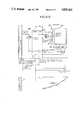
- FIG.1generally shows the conventional semiconductor integrated circuit device having the memory testing function.
- the semiconductor integrated circuit devicecomprises gate arrays 1 and 2, a random access memory (RAM) 3, normal signal input terminals 4, test signal input terminals 5, and output terminals 6.
- RAMrandom access memory
- Both the first and second interconnectionsare formed during an interconnection pattern forming process by automatically designing the interconnection layout pattern using the computer aided design (CAD) technique.
- CADcomputer aided design
- normal signalssuch as an address signal, a block select signal, a write-enable signal and a normal input data are supplied to the normal signal input terminals 4.
- the normal input datais supplied to the RAM 3 through the gate array 1 and is written into a memory cell array of the RAM 3 responsive to the write-enable signal from a block selected by the block select signal.
- a normal output data read out from the RAM 3is obtained through the gate array 2 and is outputted from the output terminals 6.
- test signalssuch as an address signal, a block select signal, a write-enable signal and a test input data are supplied to the test signal input terminals 5.
- the test input dataare supplied to the RAM 3 through the gate array 1 and is written into memory cell array of the RAM 3 responsive to the write-enable signal from a block selected by the block select signal.
- a test output data read out from the RAM 3is obtained through the gate array 2 and is outputted from the output terminals 6. It is impossible to check the state of the RAM 3 from the test output data outputted from the output terminals 6.
- the normal signal input terminals 4 and the test signal input terminals 5are provided independently, thereby resulting in a large number of input/output pins. For this reason, the number of input/output pins originally for use with the gate array is reduced because of the need to provide independent input/output pins for supporting the memory testing function. Hence, there is a problem in that the gate arrays 1 and 2 cannot be utilized effectively.
- the second interconnection of the test signal systemis designed automatically depending on the first interconnection of the normal signal system which is designed automatically.
- the second interconnectionis dependent on the kind or model of the semiconductor integrated circuit device, and the second interconnection must be designed for each kind or model of the semiconductor integrated circuit. Therefore, there are problems in that the interconnection must be drawn around wastefully and that it takes a long time to design and manufacture the semiconductor integrated circuit device.
- the propagation time of the test signaldiffers for each kind or model when testing the RAM of the semiconductor integrated circuit.
- an evaluation testsuch as evaluating the access time of the RAM cannot be carried out uniformly with respect to the different kinds or models of the semiconductor integrated circuit.
- Another and more specific object of the present inventionis to provide a semiconductor integrated circuit device having a memory testing function, in which a number of input/output pins is small, an interconnection is not drawn around wastefully, and the designing and manufacturing of the semiconductor integrated circuit device is facilitated.
- Still another object of the present inventionis to provide a semiconductor integrated circuit device having a normal mode and a test mode for testing a memory thereof, and comprises input/output buffer parts having input/output terminals, at least one gate array, at least one memory, a first interconnection for coupling the input/output buffer parts, the gate array and the memory and routed depending on a logic operation to be carried out by the semiconductor integrated circuit, and a second interconnection for coupling the input/output buffer parts, the gate array and the memory, where the second interconnection is fixed regardless of the logic operation to be carried out by the semiconductor integrated circuit.
- the input/output buffer partscomprise a first input/output part having a first terminal which is used in common as an input terminal of the first interconnection for receiving a normal input signal in the normal mode and an input terminal of the second interconnection for receiving a test signal in the test mode, and a second input/output part having a second terminal which is used in common as an output terminal of the first interconnection and an output terminal of the second interconnection.
- FIG. 1is a system block diagram generally showing an example of the conventional semiconductor integrated circuit device
- FIG. 2is a system block diagram generally showing an embodiment of the semiconductor integrated circuit device according to the present invention.
- FIG. 3is a plan view showing interconnections of the device shown in FIG.2;
- FIGS. 4A through 4Care plan views on an enlarged scale respectively showing the interconnections at predetermined regions of the device shown in FIG.3.
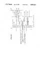
- FIG. 2generally shows an embodiment of the semiconductor integrated circuit device according to the present invention.
- the semiconductor integrated circuit devicecomprises gate arrays 10 and 11, RAMs 12 and 13, input/output parts 15i and 16i including input/output pins and input/output buffers, interconnections 17 of a test signal system, and interconnections 18a through 18d of a normal signal system.
- the input/output pins of the input/output parts 15i and 16iare used in common as input/output terminals of the interconnections 17 of the test signal system and input/output terminals of the interconnections 18a and 18d of the normal signal system.
- the interconnections 17are fixed, while the interconnections 18a through 18d are formed during an interconnection pattern forming process by automatically designing the interconnection layout pattern using the computer aided design (CAD) technique.
- CADcomputer aided design
- the present embodimentit is possible to reduce the number of input/output pins compared to the conventional device because the same input/outut pins are used in common as the input/output terminals of the interconnections 17 and the input/output terminals of the interconnections 18a and 18d.
- an interconnection (or wiring) regionis effectively utilized without the need to draw the interconnection around wastefully since the interconnections 17 of the test signal system are fixed. Accordingly, semiconductor integrated circuit device can be designed and manufactured with ease without taking a long period of time.
- the interconnections 17 of the test signal systemare the same for each kind or model of the integrated circuit device, an evaluation test of the RAM of the integrated circuit device can be carried out uniformly with respect to the different kinds or models of the integrated circuit device.
- FIG.3shows the interconnections of the embodiment shown in FIG. 2.
- FIG. 3shows the semiconductor integrated circut device in the form of a chip, and mainly shows the fixed interconnections of the test signal system.
- those parts which are the same as those corresponding parts in FIG.2are designated by the same reference numerals, and a description thereof will be omitted.
- the semiconductor integrated circuit devicecomprises an input/output terminal region 14, and input/output buffer parts 15 and 16 having input/output parts provided in the input/output terminal region 14.
- the input /output partshave input/output terminals (input/output pins) and input/output buffers.
- the fixed interconnections 17 of the test signal systemare indicated by bold lines, and these fixed interconnections 17 are fixed regardless of the kind or model of the semiconductor integrated circuit device.
- the interconnections 18a through 18d of the normal signal systemare formed in interconnection regions other than the interconnection regions of the fixed interconnections 17 in correspondence with the kind or model of the semiconductor integrated circuit device.
- the interconnections 18acouple the gate arrays 10 and 11 to the input/outut buffer part 15.
- the interconnections 18b and 18ccouple the gate arrays 10 and 11 to the RAMs 12 and 13.
- the interconnections 18dcouple the gate arrays 10 and 11 to the input/output buffer part 16.
- the fixed interconnections 17couple directly to the RAMs 12 and 13 without being routed through the gate arrays 10 and 11.
- input terminals of the fixed interconnections 17 and input terminals of the interconnections 18aare used in common at the input/output terminals of the input/output parts of the input/output buffer part 15.
- output terminals of the fixed interconnections 17 and output terminals of the interconnection 18dare used in common at the input/output terminals of the input/output parts of the input/output buffer part 16.
- FIGS.4A through 4Crespectively show on an enlarged scale the interconnections at predetermined regions A through C of the semiconductor integrated circuit device encircled by phantom lines in FIG.3.
- a black circular markindicates a terminal of the test signal system
- a white circular markindicates a terminal of the normal signal system
- a solid lineindicates a first layer interconnection
- a phantom lineindicates a second layer interconnection
- a white rhombic markindicates a connection point for connecting the first and second layer interconnections.
- the input/output buffer part 15is made up of input/output parts 15 1 , 15 2 , . . . each comprising an input/output terminal 15P and input/output buffers 15B.
- the fixed interconnections 17 of the test signal drawn out from each of the input/output parts 15 1 , 15 2 , . . .are provided within an interconnection region without being routed through the gate array 11.
- the interconnections 18a of the normal signal system drawn out from each of the input/output parts 15 1 , 15 2 , . . .are provided within interconnection regions other than the interconnection regions of the fixed interconnections 17 and are coupled to the gate array 11. In this case, input terminals of the fixed interconnections 17 and the interconnections 18a are used in common at the one of the input/output parts 15 1 , 15 2 , . . . constituting the input/output buffer part 15.
- the fixed interconnections 17 drawn out from the input/output buffer part 15couple to the RAM 12, while the fixed interconnections 17 drawn out from the RAM 12 couple to the input/output buffer part 16.
- the interconnections 18b and 18c drawn out from the gate array 10are provided within an interconnection region other than the interconnection region of the fixed interconnections 17 and couple to the RAM 12.
- the interconnection regions of the test signal system and the normal signal systemare provided in the first layer interconnection layer and the second layer interconnection layer.
- the RAM 12generally comprises an OR-AND circuit 20, a write amplifier 23, a memory cell array 24, a sense amplifier 25 and an OR circuit 26.
- the OR-AND circuit 20is a switching gate for switching the mode of the RAM 12 to a test mode when supplied with a low-level mode switching signal TM from a fixed interconnection 17' of a mode switching signal system out of the fixed interconnections 17 and to a normal mode when supplied with a high-level mode switching signal TM, for example.
- NORMAL(IN) and NORMAL(OUT)respectively denote input and output signals of the RAM 12 in the normal mode
- TEST(IN) and TEST(OUT)respectively denote input and output test signals of the RAM 12 in the test mode.
- the input/output buffer part 16is made up of input/output parts 16 1 , . . . each comprising a NOR circuit 21 and a pad 22.
- the interconnection 18d drawn out from the gate array 10 and the fixed interconnection 17 drawn out from the RAM 12are coupled to the NOR circuit 21 of the input/output part 16 1 and accordingly couples to the pad 22 thereof.
- a power source line 23is provided as a second layer fixed interconnection for supplying a power source voltage to each part of the semiconductor integrated circuit.
- a single input/output pinis used in common as the input terminals of the test signal system and the normal signal system, and the normal signal and the test signal can be obtained from the single input/output pin.
- the interconnections of the test signal systemare fixed interconnections while the interconnections of the normal signal system are formed by automatically designing the interconnection layout pattern using the computer aided design (CAD) technique.
- CADcomputer aided design
- the described embodimenthas two gate arrays and two RAMS. However, it is of course possible to provide only one gate array and only one RAM, or provide three or more gate arrays and three or more RAMS depending on the needs.
Landscapes
- Tests Of Electronic Circuits (AREA)
- Design And Manufacture Of Integrated Circuits (AREA)
- Semiconductor Integrated Circuits (AREA)
- Testing Or Measuring Of Semiconductors Or The Like (AREA)
- For Increasing The Reliability Of Semiconductor Memories (AREA)
Abstract
Description
Claims (6)
Applications Claiming Priority (2)
| Application Number | Priority Date | Filing Date | Title |
|---|---|---|---|
| JP62-163542 | 1987-06-30 | ||
| JP62163542AJP2659095B2 (en) | 1987-06-30 | 1987-06-30 | Semiconductor integrated circuit device having gate array and memory |
Publications (1)
| Publication Number | Publication Date |
|---|---|
| US4825414Atrue US4825414A (en) | 1989-04-25 |
Family
ID=15775866
Family Applications (1)
| Application Number | Title | Priority Date | Filing Date |
|---|---|---|---|
| US07/210,966Expired - LifetimeUS4825414A (en) | 1987-06-30 | 1988-06-24 | Semiconductor integrated circuit device having gate array and memory and input-output buffer |
Country Status (4)
| Country | Link |
|---|---|
| US (1) | US4825414A (en) |
| EP (1) | EP0297821A3 (en) |
| JP (1) | JP2659095B2 (en) |
| KR (1) | KR910007409B1 (en) |
Cited By (35)
| Publication number | Priority date | Publication date | Assignee | Title |
|---|---|---|---|---|
| US4956818A (en)* | 1987-10-02 | 1990-09-11 | Hitachi, Ltd. | Memory incorporating logic LSI and method for testing the same LSI |
| US4990800A (en)* | 1987-12-30 | 1991-02-05 | Samsung Electronics Co., Ltd. | Mode selector for use in semiconductor memory device |
| US5124589A (en)* | 1990-06-19 | 1992-06-23 | Mitsubishi Denki Kabushiki Kaisha | Semiconductor integrated circuit capable of synchronous and asynchronous operations and operating method therefor |
| US5146428A (en)* | 1989-02-07 | 1992-09-08 | Hitachi, Ltd. | Single chip gate array |
| US5594694A (en)* | 1995-07-28 | 1997-01-14 | Micron Quantum Devices, Inc. | Memory circuit with switch for selectively connecting an input/output pad directly to a nonvolatile memory cell |
| US5625631A (en)* | 1996-04-26 | 1997-04-29 | International Business Machines Corporation | Pass through mode for multi-chip-module die |
| US5796269A (en)* | 1996-04-09 | 1998-08-18 | Xilinx, Inc. | Composable memory array for a programmable logic device and method for implementing same |
| US5977791A (en)* | 1996-04-15 | 1999-11-02 | Altera Corporation | Embedded memory block with FIFO mode for programmable logic device |
| US6005410A (en)* | 1996-12-05 | 1999-12-21 | International Business Machines Corporation | Interconnect structure between heterogeneous core regions in a programmable array |
| US6011744A (en)* | 1997-07-16 | 2000-01-04 | Altera Corporation | Programmable logic device with multi-port memory |
| US6018490A (en)* | 1991-09-03 | 2000-01-25 | Altera Corporation | Programmable logic array integrated circuits |
| US6020760A (en)* | 1997-07-16 | 2000-02-01 | Altera Corporation | I/O buffer circuit with pin multiplexing |
| US6028446A (en)* | 1995-06-06 | 2000-02-22 | Advanced Micro Devices, Inc. | Flexible synchronous and asynchronous circuits for a very high density programmable logic device |
| US6034857A (en)* | 1997-07-16 | 2000-03-07 | Altera Corporation | Input/output buffer with overcurrent protection circuit |
| US6049223A (en)* | 1995-03-22 | 2000-04-11 | Altera Corporation | Programmable logic array integrated circuit with general-purpose memory configurable as a random access or FIFO memory |
| US6134166A (en)* | 1995-03-22 | 2000-10-17 | Altera Corporation | Programmable logic array integrated circuit incorporating a first-in first-out memory |
| US6184709B1 (en) | 1996-04-09 | 2001-02-06 | Xilinx, Inc. | Programmable logic device having a composable memory array overlaying a CLB array |
| US6262933B1 (en) | 1999-01-29 | 2001-07-17 | Altera Corporation | High speed programmable address decoder |
| US6346824B1 (en) | 1996-04-09 | 2002-02-12 | Xilinx, Inc. | Dedicated function fabric for use in field programmable gate arrays |
| US20020130681A1 (en)* | 1991-09-03 | 2002-09-19 | Cliff Richard G. | Programmable logic array integrated circuits |
| US6467017B1 (en) | 1998-06-23 | 2002-10-15 | Altera Corporation | Programmable logic device having embedded dual-port random access memory configurable as single-port memory |
| US6486702B1 (en) | 1999-07-02 | 2002-11-26 | Altera Corporation | Embedded memory blocks for programmable logic |
| US6694463B2 (en) | 2001-01-16 | 2004-02-17 | Atmel Corporation | Input/output continuity test mode circuit |
| US6720796B1 (en) | 2001-05-06 | 2004-04-13 | Altera Corporation | Multiple size memories in a programmable logic device |
| US6759870B2 (en) | 1991-09-03 | 2004-07-06 | Altera Corporation | Programmable logic array integrated circuits |
| US6812726B1 (en)* | 2002-11-27 | 2004-11-02 | Inapac Technology, Inc. | Entering test mode and accessing of a packaged semiconductor device |
| US20050024977A1 (en)* | 2000-09-21 | 2005-02-03 | Ong Adrian E. | Multiple power levels for a chip within a multi-chip semiconductor package |
| US20050162182A1 (en)* | 2002-07-25 | 2005-07-28 | Ong Adrian E. | Internally generating patterns for testing in an integrated circuit device |
| US20050289428A1 (en)* | 2000-09-21 | 2005-12-29 | Sidley Austin Brown & Wood Llp | Architecture and method for testing of an integrated circuit device |
| US7111110B1 (en) | 2002-12-10 | 2006-09-19 | Altera Corporation | Versatile RAM for programmable logic device |
| US20070067687A1 (en)* | 2001-09-28 | 2007-03-22 | Ong Adrian E | Integrated Circuit Testing Module Configured for Set-up and Hold Time Testing |
| US20070079204A1 (en)* | 2001-09-28 | 2007-04-05 | Ong Adrian E | Integrated Circuit Testing Module Including Signal Shaping Interface |
| US7466603B2 (en) | 2006-10-03 | 2008-12-16 | Inapac Technology, Inc. | Memory accessing circuit system |
| US8063650B2 (en) | 2002-11-27 | 2011-11-22 | Rambus Inc. | Testing fuse configurations in semiconductor devices |
| US8286046B2 (en) | 2001-09-28 | 2012-10-09 | Rambus Inc. | Integrated circuit testing module including signal shaping interface |
Families Citing this family (8)
| Publication number | Priority date | Publication date | Assignee | Title |
|---|---|---|---|---|
| KR100394575B1 (en)* | 2001-04-11 | 2003-08-14 | 삼성전자주식회사 | method for outputting internal information through test pin in semiconductor memory and output circuit therefore |
| JP2003316321A (en) | 2002-04-25 | 2003-11-07 | Dainippon Printing Co Ltd | Display device and electronic equipment |
| AU2003238442A1 (en) | 2002-06-06 | 2003-12-22 | Siba Spelcialty Chemicals Holding Inc. | Electroluminescent device |
| JP4887602B2 (en) | 2003-12-16 | 2012-02-29 | 大日本印刷株式会社 | Manufacturing method of organic functional device |
| AU2006332048B2 (en) | 2005-12-28 | 2012-03-15 | Yanmar Co., Ltd. | Tractor |
| US7604277B2 (en) | 2005-12-28 | 2009-10-20 | Yanmar Co., Ltd. | Working vehicle equipped with assist grip |
| JP5770720B2 (en)* | 2010-05-19 | 2015-08-26 | パナソニック株式会社 | IC current measuring device and IC current measuring adapter |
| KR102721621B1 (en)* | 2023-08-24 | 2024-10-24 | 주식회사 케이디이 | Disposable shock absorber using plastic deformation |
Citations (9)
| Publication number | Priority date | Publication date | Assignee | Title |
|---|---|---|---|---|
| US4608669A (en)* | 1984-05-18 | 1986-08-26 | International Business Machines Corporation | Self contained array timing |
| US4617479A (en)* | 1984-05-03 | 1986-10-14 | Altera Corporation | Programmable logic array device using EPROM technology |
| US4691161A (en)* | 1985-06-13 | 1987-09-01 | Raytheon Company | Configurable logic gate array |
| US4697241A (en)* | 1985-03-01 | 1987-09-29 | Simulog, Inc. | Hardware logic simulator |
| US4724531A (en)* | 1984-07-18 | 1988-02-09 | Hughes Aircraft Company | Gate array with bidirectional symmetry |
| US4736395A (en)* | 1985-05-02 | 1988-04-05 | Fujitsu Limited | Logic circuit having a test data loading function |
| US4742490A (en)* | 1984-12-28 | 1988-05-03 | Siemens Aktiengesellschaft | Integrated semiconductor memory |
| US4758476A (en)* | 1984-12-12 | 1988-07-19 | Hitachi Chemical Company, Ltd. | Polyimide precursor resin composition and semiconductor device using the same |
| US4768167A (en)* | 1986-09-30 | 1988-08-30 | International Business Machines Corporation | High speed CMOS latch with alternate data storage and test functions |
Family Cites Families (3)
| Publication number | Priority date | Publication date | Assignee | Title |
|---|---|---|---|---|
| US3961251A (en)* | 1974-12-20 | 1976-06-01 | International Business Machines Corporation | Testing embedded arrays |
| JPS6076141A (en)* | 1983-10-03 | 1985-04-30 | Nec Corp | Integrated logic circuit |
| JPS61292755A (en)* | 1985-06-20 | 1986-12-23 | Fujitsu Ltd | Semiconductor integrated circuit |
- 1987
- 1987-06-30JPJP62163542Apatent/JP2659095B2/ennot_activeExpired - Fee Related
- 1988
- 1988-06-24USUS07/210,966patent/US4825414A/ennot_activeExpired - Lifetime
- 1988-06-28EPEP88305857Apatent/EP0297821A3/ennot_activeWithdrawn
- 1988-06-30KRKR8808000Apatent/KR910007409B1/ennot_activeExpired
Patent Citations (10)
| Publication number | Priority date | Publication date | Assignee | Title |
|---|---|---|---|---|
| US4617479A (en)* | 1984-05-03 | 1986-10-14 | Altera Corporation | Programmable logic array device using EPROM technology |
| US4617479B1 (en)* | 1984-05-03 | 1993-09-21 | Altera Semiconductor Corp. | Programmable logic array device using eprom technology |
| US4608669A (en)* | 1984-05-18 | 1986-08-26 | International Business Machines Corporation | Self contained array timing |
| US4724531A (en)* | 1984-07-18 | 1988-02-09 | Hughes Aircraft Company | Gate array with bidirectional symmetry |
| US4758476A (en)* | 1984-12-12 | 1988-07-19 | Hitachi Chemical Company, Ltd. | Polyimide precursor resin composition and semiconductor device using the same |
| US4742490A (en)* | 1984-12-28 | 1988-05-03 | Siemens Aktiengesellschaft | Integrated semiconductor memory |
| US4697241A (en)* | 1985-03-01 | 1987-09-29 | Simulog, Inc. | Hardware logic simulator |
| US4736395A (en)* | 1985-05-02 | 1988-04-05 | Fujitsu Limited | Logic circuit having a test data loading function |
| US4691161A (en)* | 1985-06-13 | 1987-09-01 | Raytheon Company | Configurable logic gate array |
| US4768167A (en)* | 1986-09-30 | 1988-08-30 | International Business Machines Corporation | High speed CMOS latch with alternate data storage and test functions |
Cited By (71)
| Publication number | Priority date | Publication date | Assignee | Title |
|---|---|---|---|---|
| US4956818A (en)* | 1987-10-02 | 1990-09-11 | Hitachi, Ltd. | Memory incorporating logic LSI and method for testing the same LSI |
| US4990800A (en)* | 1987-12-30 | 1991-02-05 | Samsung Electronics Co., Ltd. | Mode selector for use in semiconductor memory device |
| US5146428A (en)* | 1989-02-07 | 1992-09-08 | Hitachi, Ltd. | Single chip gate array |
| US5124589A (en)* | 1990-06-19 | 1992-06-23 | Mitsubishi Denki Kabushiki Kaisha | Semiconductor integrated circuit capable of synchronous and asynchronous operations and operating method therefor |
| US6064599A (en)* | 1991-09-03 | 2000-05-16 | Altera Corporation | Programmable logic array integrated circuits |
| US6759870B2 (en) | 1991-09-03 | 2004-07-06 | Altera Corporation | Programmable logic array integrated circuits |
| US20040066212A1 (en)* | 1991-09-03 | 2004-04-08 | Altera Corporation | Programmable logic array integrated circuits |
| US20020130681A1 (en)* | 1991-09-03 | 2002-09-19 | Cliff Richard G. | Programmable logic array integrated circuits |
| US6134173A (en)* | 1991-09-03 | 2000-10-17 | Altera Corporation | Programmable logic array integrated circuits |
| US6023439A (en)* | 1991-09-03 | 2000-02-08 | Altera Corporation | Programmable logic array integrated circuits |
| US6018490A (en)* | 1991-09-03 | 2000-01-25 | Altera Corporation | Programmable logic array integrated circuits |
| US6897679B2 (en) | 1991-09-03 | 2005-05-24 | Altera Corporation | Programmable logic array integrated circuits |
| US6340897B1 (en) | 1995-03-22 | 2002-01-22 | Altera Corporation | Programmable logic array integrated circuit with general-purpose memory configurable as a random access or FIFO memory |
| US6218860B1 (en) | 1995-03-22 | 2001-04-17 | Altera Corporation | Programmable logic array integrated circuit incorporating a first-in first-out memory |
| US6134166A (en)* | 1995-03-22 | 2000-10-17 | Altera Corporation | Programmable logic array integrated circuit incorporating a first-in first-out memory |
| US6049223A (en)* | 1995-03-22 | 2000-04-11 | Altera Corporation | Programmable logic array integrated circuit with general-purpose memory configurable as a random access or FIFO memory |
| US6028446A (en)* | 1995-06-06 | 2000-02-22 | Advanced Micro Devices, Inc. | Flexible synchronous and asynchronous circuits for a very high density programmable logic device |
| US5896400A (en)* | 1995-07-28 | 1999-04-20 | Micron Technology, Inc. | Memory circuit with switch for selectively connecting an input/output pad directly to a nonvolatile memory cell |
| US6094377A (en)* | 1995-07-28 | 2000-07-25 | Micron Technology, Inc. | Memory circuit with switch for selectively connecting an input/output pad directly to a nonvolatile memory cell |
| US5706235A (en)* | 1995-07-28 | 1998-01-06 | Micron Quantum Devices, Inc. | Memory circuit with switch for selectively connecting an I/O pad directly to a nonvolatile memory cell and method for operating same |
| US5594694A (en)* | 1995-07-28 | 1997-01-14 | Micron Quantum Devices, Inc. | Memory circuit with switch for selectively connecting an input/output pad directly to a nonvolatile memory cell |
| US6184709B1 (en) | 1996-04-09 | 2001-02-06 | Xilinx, Inc. | Programmable logic device having a composable memory array overlaying a CLB array |
| US5796269A (en)* | 1996-04-09 | 1998-08-18 | Xilinx, Inc. | Composable memory array for a programmable logic device and method for implementing same |
| US6346824B1 (en) | 1996-04-09 | 2002-02-12 | Xilinx, Inc. | Dedicated function fabric for use in field programmable gate arrays |
| US5886538A (en)* | 1996-04-09 | 1999-03-23 | Xilinx, Inc. | Composable memory array for a programmable logic device and method implementing same |
| US5977791A (en)* | 1996-04-15 | 1999-11-02 | Altera Corporation | Embedded memory block with FIFO mode for programmable logic device |
| US6242946B1 (en) | 1996-04-15 | 2001-06-05 | Altera Corporation | Embedded memory block with FIFO mode for programmable logic device |
| US5625631A (en)* | 1996-04-26 | 1997-04-29 | International Business Machines Corporation | Pass through mode for multi-chip-module die |
| US6005410A (en)* | 1996-12-05 | 1999-12-21 | International Business Machines Corporation | Interconnect structure between heterogeneous core regions in a programmable array |
| US6054873A (en)* | 1996-12-05 | 2000-04-25 | International Business Machines Corporation | Interconnect structure between heterogeneous core regions in a programmable array |
| US6219284B1 (en) | 1997-07-16 | 2001-04-17 | Altera Corporation | Programmable logic device with multi-port memory |
| US6259588B1 (en) | 1997-07-16 | 2001-07-10 | Altera Corporation | Input/output buffer with overcurrent protection circuit |
| US6034857A (en)* | 1997-07-16 | 2000-03-07 | Altera Corporation | Input/output buffer with overcurrent protection circuit |
| US6285211B1 (en) | 1997-07-16 | 2001-09-04 | Altera Corporation | I/O buffer circuit with pin multiplexing |
| US6151258A (en)* | 1997-07-16 | 2000-11-21 | Quickturn Design Systems, Inc. | Programmable logic device with multi-port memory |
| US6011744A (en)* | 1997-07-16 | 2000-01-04 | Altera Corporation | Programmable logic device with multi-port memory |
| US6011730A (en)* | 1997-07-16 | 2000-01-04 | Altera Corporation | Programmable logic device with multi-port memory |
| US6020760A (en)* | 1997-07-16 | 2000-02-01 | Altera Corporation | I/O buffer circuit with pin multiplexing |
| US6467017B1 (en) | 1998-06-23 | 2002-10-15 | Altera Corporation | Programmable logic device having embedded dual-port random access memory configurable as single-port memory |
| US6262933B1 (en) | 1999-01-29 | 2001-07-17 | Altera Corporation | High speed programmable address decoder |
| US6459303B1 (en) | 1999-01-29 | 2002-10-01 | Altera Corporation | High speed programmable address decoder |
| US6593772B2 (en) | 1999-07-02 | 2003-07-15 | Altera Corporation | Embedded memory blocks for programmable logic |
| US6486702B1 (en) | 1999-07-02 | 2002-11-26 | Altera Corporation | Embedded memory blocks for programmable logic |
| US7444575B2 (en) | 2000-09-21 | 2008-10-28 | Inapac Technology, Inc. | Architecture and method for testing of an integrated circuit device |
| US20050024977A1 (en)* | 2000-09-21 | 2005-02-03 | Ong Adrian E. | Multiple power levels for a chip within a multi-chip semiconductor package |
| US7240254B2 (en) | 2000-09-21 | 2007-07-03 | Inapac Technology, Inc | Multiple power levels for a chip within a multi-chip semiconductor package |
| US20050289428A1 (en)* | 2000-09-21 | 2005-12-29 | Sidley Austin Brown & Wood Llp | Architecture and method for testing of an integrated circuit device |
| US6694463B2 (en) | 2001-01-16 | 2004-02-17 | Atmel Corporation | Input/output continuity test mode circuit |
| US6720796B1 (en) | 2001-05-06 | 2004-04-13 | Altera Corporation | Multiple size memories in a programmable logic device |
| US8286046B2 (en) | 2001-09-28 | 2012-10-09 | Rambus Inc. | Integrated circuit testing module including signal shaping interface |
| US8001439B2 (en) | 2001-09-28 | 2011-08-16 | Rambus Inc. | Integrated circuit testing module including signal shaping interface |
| US10114073B2 (en) | 2001-09-28 | 2018-10-30 | Rambus Inc. | Integrated circuit testing |
| US9116210B2 (en) | 2001-09-28 | 2015-08-25 | Rambus Inc. | Integrated circuit testing module including signal shaping interface |
| US20070067687A1 (en)* | 2001-09-28 | 2007-03-22 | Ong Adrian E | Integrated Circuit Testing Module Configured for Set-up and Hold Time Testing |
| US20070079204A1 (en)* | 2001-09-28 | 2007-04-05 | Ong Adrian E | Integrated Circuit Testing Module Including Signal Shaping Interface |
| US8166361B2 (en) | 2001-09-28 | 2012-04-24 | Rambus Inc. | Integrated circuit testing module configured for set-up and hold time testing |
| US20050162182A1 (en)* | 2002-07-25 | 2005-07-28 | Ong Adrian E. | Internally generating patterns for testing in an integrated circuit device |
| US7313740B2 (en) | 2002-07-25 | 2007-12-25 | Inapac Technology, Inc. | Internally generating patterns for testing in an integrated circuit device |
| US8717052B2 (en) | 2002-11-27 | 2014-05-06 | Rambus Inc. | Testing fuse configurations in semiconductor devices |
| US7259582B2 (en) | 2002-11-27 | 2007-08-21 | Inapac Technology, Inc. | Bonding pads for testing of a semiconductor device |
| US6812726B1 (en)* | 2002-11-27 | 2004-11-02 | Inapac Technology, Inc. | Entering test mode and accessing of a packaged semiconductor device |
| US8063650B2 (en) | 2002-11-27 | 2011-11-22 | Rambus Inc. | Testing fuse configurations in semiconductor devices |
| US6882171B2 (en)* | 2002-11-27 | 2005-04-19 | Inapac Technology, Inc. | Bonding pads for testing of a semiconductor device |
| US20050204223A1 (en)* | 2002-11-27 | 2005-09-15 | Ong Adrian E. | Bonding pads for testing of a semiconductor device |
| US9568544B2 (en) | 2002-11-27 | 2017-02-14 | Rambus Inc. | Testing fuse configurations in semiconductor devices |
| US10302696B2 (en) | 2002-11-27 | 2019-05-28 | Rambus Inc. | Testing fuse configurations in semiconductor devices |
| US11009548B2 (en) | 2002-11-27 | 2021-05-18 | Rambus Inc. | Testing fuse configurations in semiconductor devices |
| US7480763B2 (en) | 2002-12-10 | 2009-01-20 | Altera Corporation | Versatile RAM for a programmable logic device |
| US20060294293A1 (en)* | 2002-12-10 | 2006-12-28 | Altera Corporation | Versatile RAM for a programmable logic device |
| US7111110B1 (en) | 2002-12-10 | 2006-09-19 | Altera Corporation | Versatile RAM for programmable logic device |
| US7466603B2 (en) | 2006-10-03 | 2008-12-16 | Inapac Technology, Inc. | Memory accessing circuit system |
Also Published As
| Publication number | Publication date |
|---|---|
| KR910007409B1 (en) | 1991-09-25 |
| EP0297821A2 (en) | 1989-01-04 |
| JP2659095B2 (en) | 1997-09-30 |
| KR890001076A (en) | 1989-03-18 |
| JPS647635A (en) | 1989-01-11 |
| EP0297821A3 (en) | 1990-02-07 |
Similar Documents
| Publication | Publication Date | Title |
|---|---|---|
| US4825414A (en) | Semiconductor integrated circuit device having gate array and memory and input-output buffer | |
| US5509019A (en) | Semiconductor integrated circuit device having test control circuit in input/output area | |
| US4855958A (en) | Semiconductor integrated circuit device having logic macro and random access memory macro | |
| US6806730B2 (en) | Method and system for use of an embedded field programmable gate array interconnect for flexible I/O connectivity | |
| EP0143624B1 (en) | Dynamic semiconductor memory device having divided memory cell blocks | |
| US4566082A (en) | Memory pack addressing system | |
| US5416919A (en) | Semiconductor integrated circuit with functional blocks capable of being individually tested externally | |
| US5384533A (en) | Testing method, testing circuit and semiconductor integrated circuit having testing circuit | |
| US4833620A (en) | Method for fabricating a 1-chip microcomputer | |
| EP0408353B1 (en) | Semiconductor integrated circuit | |
| US4180772A (en) | Large-scale integrated circuit with integral bi-directional test circuit | |
| US5930187A (en) | One-chip LSI including a general memory and a logic | |
| JPH0750450B2 (en) | Redundant memory array | |
| US5373467A (en) | Solid state memory device capable of providing data signals on 2N data lines or N data lines | |
| US6601197B1 (en) | Semiconductor memory device | |
| US5177573A (en) | Semiconductor integrated circuit device | |
| US5436862A (en) | IC card including multiple connectors providing memory write production | |
| US6442668B2 (en) | Bus control system | |
| US5029133A (en) | VLSI chip having improved test access | |
| US20080028104A1 (en) | Semiconductor device and operation control method of semiconductor device | |
| US5821798A (en) | Method for determining whether bi-directional or unidirectional data line circuits are used | |
| US5463560A (en) | Semiconductor integrated circuit device | |
| US4858175A (en) | Monolithic semi-custom IC having standard LSI sections and coupling gate array sections | |
| EP0265913A2 (en) | Semi-custom-made integrated circuit device | |
| KR100331551B1 (en) | Merged memory and logic semiconductor device having bist circuit |
Legal Events
| Date | Code | Title | Description |
|---|---|---|---|
| AS | Assignment | Owner name:FUJITSU LIMITED, 1015, KAMIKODANAKA, NAKAHARA-KU, Free format text:ASSIGNMENT OF ASSIGNORS INTEREST.;ASSIGNOR:KAWATA, MITSUYA;REEL/FRAME:004903/0427 Effective date:19880621 Owner name:FUJITSU LIMITED, JAPAN Free format text:ASSIGNMENT OF ASSIGNORS INTEREST;ASSIGNOR:KAWATA, MITSUYA;REEL/FRAME:004903/0427 Effective date:19880621 | |
| STCF | Information on status: patent grant | Free format text:PATENTED CASE | |
| FPAY | Fee payment | Year of fee payment:4 | |
| FEPP | Fee payment procedure | Free format text:PAYOR NUMBER ASSIGNED (ORIGINAL EVENT CODE: ASPN); ENTITY STATUS OF PATENT OWNER: LARGE ENTITY | |
| FPAY | Fee payment | Year of fee payment:8 | |
| FPAY | Fee payment | Year of fee payment:12 | |
| AS | Assignment | Owner name:FUJITSU MICROELECTRONICS LIMITED,JAPAN Free format text:ASSIGNMENT OF ASSIGNOR'S RIGHT, TITLE AND INTEREST;ASSIGNOR:FUJITSU LIMITED;REEL/FRAME:024035/0224 Effective date:20100218 Owner name:FUJITSU MICROELECTRONICS LIMITED, JAPAN Free format text:ASSIGNMENT OF ASSIGNOR'S RIGHT, TITLE AND INTEREST;ASSIGNOR:FUJITSU LIMITED;REEL/FRAME:024035/0224 Effective date:20100218 |