US4821277A - Super-luminescent diode - Google Patents
Super-luminescent diodeDownload PDFInfo
- Publication number
- US4821277A US4821277AUS07/040,977US4097787AUS4821277AUS 4821277 AUS4821277 AUS 4821277AUS 4097787 AUS4097787 AUS 4097787AUS 4821277 AUS4821277 AUS 4821277A
- Authority
- US
- United States
- Prior art keywords
- angle
- end faces
- beam path
- width
- path
- Prior art date
- Legal status (The legal status is an assumption and is not a legal conclusion. Google has not performed a legal analysis and makes no representation as to the accuracy of the status listed.)
- Expired - Lifetime
Links
Images
Classifications
- H—ELECTRICITY
- H10—SEMICONDUCTOR DEVICES; ELECTRIC SOLID-STATE DEVICES NOT OTHERWISE PROVIDED FOR
- H10H—INORGANIC LIGHT-EMITTING SEMICONDUCTOR DEVICES HAVING POTENTIAL BARRIERS
- H10H20/00—Individual inorganic light-emitting semiconductor devices having potential barriers, e.g. light-emitting diodes [LED]
- H10H20/80—Constructional details
- H10H20/81—Bodies
- H10H20/822—Materials of the light-emitting regions
- H10H20/824—Materials of the light-emitting regions comprising only Group III-V materials, e.g. GaP
- G—PHYSICS
- G02—OPTICS
- G02B—OPTICAL ELEMENTS, SYSTEMS OR APPARATUS
- G02B6/00—Light guides; Structural details of arrangements comprising light guides and other optical elements, e.g. couplings
- G02B6/24—Coupling light guides
- G02B6/42—Coupling light guides with opto-electronic elements
- G02B6/4201—Packages, e.g. shape, construction, internal or external details
- G02B6/4202—Packages, e.g. shape, construction, internal or external details for coupling an active element with fibres without intermediate optical elements, e.g. fibres with plane ends, fibres with shaped ends, bundles
- G02B6/4203—Optical features
- H—ELECTRICITY
- H01—ELECTRIC ELEMENTS
- H01S—DEVICES USING THE PROCESS OF LIGHT AMPLIFICATION BY STIMULATED EMISSION OF RADIATION [LASER] TO AMPLIFY OR GENERATE LIGHT; DEVICES USING STIMULATED EMISSION OF ELECTROMAGNETIC RADIATION IN WAVE RANGES OTHER THAN OPTICAL
- H01S5/00—Semiconductor lasers
- H01S5/10—Construction or shape of the optical resonator, e.g. extended or external cavity, coupled cavities, bent-guide, varying width, thickness or composition of the active region
- H—ELECTRICITY
- H10—SEMICONDUCTOR DEVICES; ELECTRIC SOLID-STATE DEVICES NOT OTHERWISE PROVIDED FOR
- H10H—INORGANIC LIGHT-EMITTING SEMICONDUCTOR DEVICES HAVING POTENTIAL BARRIERS
- H10H20/00—Individual inorganic light-emitting semiconductor devices having potential barriers, e.g. light-emitting diodes [LED]
- H10H20/042—Superluminescent diodes
Definitions
- the inventionrelates to a super-luminescent diode having a radiation confining region whose axis of symmetry is nonperpendicular to one of the diode's end faces.
- Ser. No. 040,976entitled “Optical Coupling System” by Minora Toda et al.
- Ser. No. 040,979entitled “Super Luminescent Diode” by G. A. Alphonse et al.
- Ser. No. 040,978entitled "Low Coherence Optical System Having Reflective Means" by G. A. Alphonse all filed concurrently herewith and assigned to the assignee of the present invention.
- High power radiation emitting devicessuch as semiconductor lasers
- Gainwhich is necessary for these high power devices, results from a population inversion which occurs when applied current is increased.
- the end faces of the bodyform a resonant cavity such that radiation generated in the active layer is partially reflected back into the semiconductor body by an end face toward the opposing end face.
- the increase in gaincauses lasing action to occur.
- Lasersemit a narrow band of highly coherent radiation having a coherence length of approximately 2 centimeters(cm).
- Coherent radiationor radiation having a high spectral modulation
- fiber optic gyroscopeswhich require high power devices which emit radiation having low coherence.
- Other devicessuch as light emitting diodes (LED's) emit a broad band of radiation but operate at low power, insufficient for high power applications.
- LED'slight emitting diodes
- Super-luminescent diodesprovide a high power output of broad band low coherent radiation, that being radiation having a coherence length of less than about 200 micrometers ( ⁇ m) and typically about 50 ⁇ m.
- An SLDtypically has a structure similar to that of a laser, with lasing being prevented by antireflection coating formed on the end faces. These coatings must reduce the reflectivity of the end faces to about 10 -5 or less to prevent lasing in a high power SLD and further, this reflectivity must be reduced to about 10 -6 to achieve low spectral modulation.
- Spectral modulationis the percentage ratio of the difference between the maximum and minimum power output divided by the sum of the maximum and minimum power output and low spectral modulation is 5% or less modulation.
- low reflectivity of about 10 31 6 at the end facesis difficult to obtain consistently for a given output wavelength and even a slight temperature change which alters the output wavelength will change the reflectivity, thus making the manufacture of low spectral modulation SLDs extremely difficult.
- SLD structuresutilize a stripe interrupt geometry in which a metallized stripe is formed over a portion of an active region. This stripe extends from one end face towards but not up to the opposing end face. During device operation of these SLDs a reflecting interface is formed under the end of the metallized stripe which does not extend to the opposing end face. This interface is formed due to differences in propagation characteristics in the active region, where current is not supplied by the metallized stripe and results in high spectral modulation even at moderate power levels.
- an SLDhas been limited to a maximum output power of about 7 mw continuous wave (cw) and has had high spectral modulation, typically 50% at maximum power and 20% at half power.
- cwcontinuous wave
- a low coherence light emitting devicecomprises a body having a pair of end faces.
- the devicecontains a current confining structure therein such as to form an effective optical beam path between the end faces.
- the axis of symmetry of the structureis formed at an angle relative to the direction perpendicular to at least one of the end faces and the tangent of the angle is greater than or equal to the width of the effective optical beam path divided by the length of the body between the end faces.
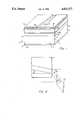
- FIG. 1is a perspective view of a light emitting device of the invention.
- FIG. 2is a top view of an optical system for coupling radiation from the light emitting device of the present invention into an optical fiber.
- a light-emitting device 1comprises a body 2 having first and second opposed end faces 3 and 4, respectively, and sidewalls 6 extending therebetween.
- the body 2includes a substrate 12 having a first cladding layer 14 thereon, an active layer 16 overlying the first cladding layer 14, a second cladding layer 18 overlying the active layer 16, and a capping layer 20 overlying the second cladding layer 18.
- a means for electrically contacting the body 2comprises a first electrical contact 30 which overlies the surface of the substrate 12 opposite the first cladding layer 14 and a second electrical contact 32 which overlies the capping layer 20 in the aperture 24 and insulating layer 22.
- the substrate 12, first cladding layer 14, and capping layer 20are of one conductivity type and the second cladding layer 18 is of the opposite conductivity type.
- the refractive index of the active layer 16should be greater than the refractive index of both the first and second cladding layers 14 and 18, respectively.
- the bodyis typically composed of binary group III-V compounds such as GaAs and alloys of such compounds.
- the substrate 12is typically composed of N-type GaAs about 100 micrometers ( ⁇ m) thick and has a first major surface parallel to or slightly misoriented from the (100) crystallographic plane.
- the first cladding layer 14typically combines the functions of a buffer layer and a cladding layer.
- the first and second cladding layers 14 and 18 respectively,are about 1.5 ⁇ m thick and are typically composed of Al x Ga l-x As where x is generally between about 0.3 and 0.4 and typically about 0.4.
- the active layer 16is typically about 0.08 ⁇ m thick and is generally composed of Al x Ga l-x As where x is between about 0 and 0.1, depending on the wavelength to be emitted.
- the capping layer 20is typically about 0.5 ⁇ m thick and is typically composed of N-type GaAs with zinc diffused therethrough in the region of the aperture 24.
- the insulating layer 22is typically about 0.01 ⁇ m thick and is preferably composed of silicon oxide deposited by pyrolytic decomposition of a silicon-containing gas, such as silane, in oxygen or water vapor.
- the meansis a current confining structure, such as the second electrical contact 32 in the aperture 24, which is in the shape of a linear stripe about 5 ⁇ m wide in the lateral direction, that being the direction perpendicular to the planes of the sidewalls 6.
- an additional current confining structureis formed such as by employing the capping layer 20 to form a current blocking layer.
- the current confining structureextends between the pair of opposed parallel end faces, 3 and 4 respectively, and has an axis of symmetry which is at an angle ⁇ relative to the direction perpendicular to the end faces.
- the tangent of the angle ⁇must be greater than or equal to the effective width of the optical beam path in the device divided by the length of the body between the first and second end faces 3 and 4, respectively. This minimizes the Fabry-Perot reflections which occur in a laser cavity due to reflections occurring between the end faces 3 and 4 respectively.
- the effective width of the optical beam in the device 1is not the width of the aperture 24 since the effective width of the optical beam will extend on each side of the aperture 24. If merely the width of the structure is relied upon as the effective width of the optical beam, then an unacceptable high modulation output will be emitted. For example, an SLD was formed with ⁇ being about 5°.
- the devicehad a 5 ⁇ m width stripe and was about 200 ⁇ m in length.
- the tangent of the angle ⁇was about 0.087 and was much greater than the width of the stripe divided by the length of the body.
- a high modulation output of about 30%was emitted in this device.
- this devicehad an effective beam path width of about 40 ⁇ m. Therefore, the tangent of the angle ⁇ was less than the effective width of the optical path divided by the length of the body and was thereby insufficient to adequately reduce the Fabry-Perot feedback in the gain region.
- the width of the effective optical beam pathis typically determined by obtaining an intensity beam profile by attaching a camera and a linear array of detectors to a microscope.
- the cameraprovides a direct view of the emitting facet and the output of the detectors provides an intensity beam profile.
- a vidicon camerain which a charge density pattern is formed on a photoconductor may be scanned with an electron beam in a single line to obtain the intensity beam profile.
- the beam widthis determined by the half width of the beam profile.
- the 2 ⁇ or 3 ⁇ widths of the profilemay be used to further reduce any possible feedback.
- the angle ⁇must have a value such that 20 exceeds the critical value for lateral reflection, that being the angle at which there is no refracted ray and thereby total internal reflection exists.
- the active layer 16has differences in its effective refractive index between that portion of the active layer 16 containing the optical beam path and the remaining portion of the active layer. These differences in refractive index serve as boundaries which confine radiation within the optical beam path of the device, providing total internal reflection and thereby resulting in high spectral modulation. Therefore, the angle 2 ⁇ must be greater than the critical angle to prevent reflections in the opticaI beam path at these boundaries.
- the critical angle ⁇ cis determined as follows:
- n 1is the effective refractive index of the active layer 16 containing the optical beam and is typically about 3.355 for AlGaAs and n 2 is the effective refractive index of the remaining portion of the active layer and is typically about 3.35 for AlGaAs. Therefore, ⁇ c is typically about 3.13°/2 and the angle ⁇ must be greater than 3.13°/2 and is chosen to be about 5° to account for diffraction spread.
- the angle ⁇may be about equal to the Brewster angle which is equal to the inverse tangent of the refractive index of the medium adjacent the first end face 3, divided by the transverse effective refractive index for light propagating between the end faces.
- the medium adjacent the first end face 3is typically air having a refractive index of about 1 and the refractive index of the body 2 is typically 3.35 for GaAs devices.
- the Brewster angleis typically about 16.6°.
- the radiation vibrating in the plane of incidenceis not reflected, thus resulting in radiation which is predominantly polarized.
- the reflected and refracted raysare 90° apart resulting in a non-reflective condition at the emitting end face. This condition allows the elimination of antireflection coatings on the devices' end faces which are typically used to increase output.
- the emitted radiationwill be nonperpendicular relative to the first end face 3 having an output angle ⁇ determined by: ##EQU1## Where n 1 , is the transverse effective refractive index of the device 1 and n 2 is the refractive index of the medium adjacent the first end face.
- n 1is the transverse effective refractive index of the device 1
- n 2is the refractive index of the medium adjacent the first end face.
- Optical coupling from the device 1 to a receiving device such as an optical fiber 50may be obtained by inclining the fiber's end face 54 such that it is nonperpendicular relative to the fiber's axis and radiation propagates along the fiber's axis such as disclosed by Minoru Toda in a copending U.S. patent application Ser. No. 040,976. Further, a reflective coating is preferably positioned adjacent the second end face 4 to provide a means for redirecting a portion of the radiation back into the device such as disclosed by Gerard A. Alphonse in copending U.S. application Ser. No.
- the body 2may be fabricated using liquid-phase epitaxy techniques to deposit the layers. Suitable liquid-phase epitaxy techniques have been disclosed by Nelson in U.S. Pat. No. 3,565,702 and Lockwood et al. in U.S. Pat. No. 3,753,801, both incorporated herein by reference.
- the aperture 24is formed in the silicon oxide insulating layer 22 by first forming a photoresist layer having an angled stripe aperture therein, over the insulating layer 22 which is then etched by a suitable etchant such as buffered hydrofluoric acid.
- current confining structuresmay be formed by other means, for example, ridge guide structures may be formed in which an active layer or a waveguide layer provide the current confining structure of the present invention.
- the first electrical contact 30is preferably composed of sequentially deposited germanium, gold, nickel, and gold layers.
- the second electrical contact 32is preferably composed of titanium, platinum and gold layers which are sequentially deposited onto a zinc or cadmium diffused surface.
- a bias voltage of the proper polarityis applied to the electrical contacts 30 and 32 respectively, producing light emission in the active region.
- the aperture 24provides a means for reducing on-axis reflections of light between the end faces resulting in an emission having low coherence.
Landscapes
- Physics & Mathematics (AREA)
- General Physics & Mathematics (AREA)
- Optics & Photonics (AREA)
- Condensed Matter Physics & Semiconductors (AREA)
- Electromagnetism (AREA)
- Led Devices (AREA)
Abstract
Description
θ.sub.c =Sin.sup.-1 [1-(.sup.n 2/n.sub.1).sup.2 9 .sup.1/2
Claims (9)
Priority Applications (2)
| Application Number | Priority Date | Filing Date | Title |
|---|---|---|---|
| US07/040,977US4821277A (en) | 1987-04-20 | 1987-04-20 | Super-luminescent diode |
| CA000561108ACA1298645C (en) | 1987-04-20 | 1988-03-10 | Super-luminescent diode |
Applications Claiming Priority (1)
| Application Number | Priority Date | Filing Date | Title |
|---|---|---|---|
| US07/040,977US4821277A (en) | 1987-04-20 | 1987-04-20 | Super-luminescent diode |
Publications (1)
| Publication Number | Publication Date |
|---|---|
| US4821277Atrue US4821277A (en) | 1989-04-11 |
Family
ID=21914042
Family Applications (1)
| Application Number | Title | Priority Date | Filing Date |
|---|---|---|---|
| US07/040,977Expired - LifetimeUS4821277A (en) | 1987-04-20 | 1987-04-20 | Super-luminescent diode |
Country Status (2)
| Country | Link |
|---|---|
| US (1) | US4821277A (en) |
| CA (1) | CA1298645C (en) |
Cited By (29)
| Publication number | Priority date | Publication date | Assignee | Title |
|---|---|---|---|---|
| US4872180A (en)* | 1989-06-16 | 1989-10-03 | Gte Laboratories Incorporated | Method for reducing facet reflectivities of semiconductor light sources and device thereof |
| US4942366A (en)* | 1989-03-21 | 1990-07-17 | General Electric Company | Amplifier device with coupled surface emitting grating |
| US4958355A (en)* | 1989-03-29 | 1990-09-18 | Rca Inc. | High performance angled stripe superluminescent diode |
| US5008889A (en)* | 1989-11-06 | 1991-04-16 | Wilson Keith E | High-accuracy wavelength stabilization of angled-stripe super luminescent laser diode sources |
| US5034955A (en)* | 1988-11-30 | 1991-07-23 | Oki Electric Industry Co., Ltd. | Superluminescent diode |
| US5223722A (en)* | 1991-03-26 | 1993-06-29 | Mitsubishi Denki Kabushiki Kaisha | Superluminescent diode |
| US5329134A (en)* | 1992-01-10 | 1994-07-12 | International Business Machines Corporation | Superluminescent diode having a quantum well and cavity length dependent threshold current |
| WO1996027929A1 (en)* | 1995-03-07 | 1996-09-12 | British Telecommunications Public Limited Company | A laser |
| US5629917A (en)* | 1994-12-05 | 1997-05-13 | Kamatani; Yasuo | Integrated optical pick-up emits light beams of selective wavelengths to an optical disk with multiple data layers |
| EP0902978A4 (en)* | 1996-06-05 | 2000-02-23 | Sarnoff Corp | LIGHT EMITTING SEMICONDUCTOR DEVICE |
| US6034380A (en)* | 1997-10-07 | 2000-03-07 | Sarnoff Corporation | Electroluminescent diode with mode expander |
| US6097743A (en)* | 1998-06-16 | 2000-08-01 | Sarnoff Corporation | Superluminescent diode and optical amplifier with wavelength stabilization using WDM couplers and back output light |
| US6175446B1 (en) | 1998-09-23 | 2001-01-16 | Sarnoff Corporation | Polarization-independent semiconductor optical amplifier |
| US6184542B1 (en) | 1998-06-16 | 2001-02-06 | Princeton Lightwave | Superluminescent diode and optical amplifier with extended bandwidth |
| US6339606B1 (en) | 1998-06-16 | 2002-01-15 | Princeton Lightwave, Inc. | High power semiconductor light source |
| US6430204B1 (en)* | 1998-08-19 | 2002-08-06 | Hitachi, Ltd. | Semiconductor laser device and optical processing system using the device |
| US6593602B2 (en)* | 2000-08-30 | 2003-07-15 | Stanley Electric Co., Ltd. | Edge emission type semiconductor device for emitting super luminescent light, its manufacture and spatial optical communication device |
| US20040061122A1 (en)* | 2002-09-27 | 2004-04-01 | Gerard Alphonse | Light emitting device with low back facet reflections |
| US20040062507A1 (en)* | 2002-09-27 | 2004-04-01 | Mitsubish Denki Kabushiki Kaisha | Semiconductor optical device |
| US20040065890A1 (en)* | 2002-09-27 | 2004-04-08 | Gerard Alphonse | Narrow spectral width light emitting devices |
| US6741352B2 (en)* | 2000-12-25 | 2004-05-25 | Fuji Photo Film Co., Ltd. | Sensor utilizing attenuated total reflection |
| US6804281B1 (en)* | 2001-01-23 | 2004-10-12 | James N. Walpole | Large modal volume semiconductor laser system with spatial mode filter |
| US20050105100A1 (en)* | 2003-11-17 | 2005-05-19 | Asml Holding N.V. | Optical position measuring system and method using a low coherence light source |
| US20090022194A1 (en)* | 2004-08-05 | 2009-01-22 | Akiyoshi Watanabe | Semiconductor laser device and semiconductor laser device array |
| US20090310634A1 (en)* | 2004-04-27 | 2009-12-17 | Oclaro | Stabilized laser source with very high relative feedback and narrow bandwidth |
| US20110292496A1 (en)* | 2010-01-08 | 2011-12-01 | Stefan Mohrdiek | Laser system with highly linear output |
| US8259304B2 (en) | 2010-05-26 | 2012-09-04 | Gerard A Alphonse | Broadband discrete spectrum optical source |
| US8269977B2 (en) | 2010-05-26 | 2012-09-18 | Gerard A Alphonse | Discrete spectrum broadband optical source |
| US10876840B2 (en) | 2018-06-15 | 2020-12-29 | The Charles Stark Draper Laboratory, Inc. | Second-order passive ring interferometer sensor and method |
Citations (3)
| Publication number | Priority date | Publication date | Assignee | Title |
|---|---|---|---|---|
| US4251780A (en)* | 1978-07-03 | 1981-02-17 | Xerox Corporation | Stripe offset geometry in injection lasers to achieve transverse mode control |
| US4323856A (en)* | 1976-07-02 | 1982-04-06 | U.S. Philips Corporation | Injection laser |
| US4432091A (en)* | 1981-02-06 | 1984-02-14 | Hitachi, Ltd. | Semiconductor laser device |
- 1987
- 1987-04-20USUS07/040,977patent/US4821277A/ennot_activeExpired - Lifetime
- 1988
- 1988-03-10CACA000561108Apatent/CA1298645C/ennot_activeExpired - Lifetime
Patent Citations (3)
| Publication number | Priority date | Publication date | Assignee | Title |
|---|---|---|---|---|
| US4323856A (en)* | 1976-07-02 | 1982-04-06 | U.S. Philips Corporation | Injection laser |
| US4251780A (en)* | 1978-07-03 | 1981-02-17 | Xerox Corporation | Stripe offset geometry in injection lasers to achieve transverse mode control |
| US4432091A (en)* | 1981-02-06 | 1984-02-14 | Hitachi, Ltd. | Semiconductor laser device |
Non-Patent Citations (21)
| Title |
|---|
| D. R. Kaplan et al., "Exact Calculation Of The Reflection Coefficient For Coated Optical Waveguide Devices," AT&T Bell Laboratories Technical Journal, vol. 63, No. 6, Jul.-Aug. 1984, pp. 857-877. |
| D. R. Kaplan et al., Exact Calculation Of The Reflection Coefficient For Coated Optical Waveguide Devices, AT&T Bell Laboratories Technical Journal, vol. 63, No. 6, Jul. Aug. 1984, pp. 857 877.* |
| D. R. Scifres et al., "GaAs/GaAlAs Diode Lasers With Angled Pumping Stripes," IEEE Journal of Quantum Electronics, vol. QE-14, No. 4, Apr. 1978, pp. 223-227. |
| D. R. Scifres et al., GaAs/GaAlAs Diode Lasers With Angled Pumping Stripes, IEEE Journal of Quantum Electronics, vol. QE 14, No. 4, Apr. 1978, pp. 223 227.* |
| G. A. Alphonse et al., "High-Power Superluminescent Diodes," OSC Conference, Jan. 19-21, 1987. |
| G. A. Alphonse et al., High Power Superluminescent Diodes, OSC Conference, Jan. 19 21, 1987.* |
| G. A. Alphonse, Superluminescent Diode Development, May 1986.* |
| I. Ladany et al., "Scandium Oxide Antireflection Coatings For Superluminescent LEDs" Applied Optics, vol. 25, No. 4, Feb. 15, 1986, pp. 472-473. |
| I. Ladany et al., Scandium Oxide Antireflection Coatings For Superluminescent LEDs Applied Optics, vol. 25, No. 4, Feb. 15, 1986, pp. 472 473.* |
| I. P. Kaminow et al., "Measurement of the Modal Reflectivity Of An Antireflection Coating On A Superluminescent Diode," IEEE Journal Of Quantum Electronics, vol. QE-19, No. 4, Apr. 1983, pp. 493-495. |
| I. P. Kaminow et al., Measurement of the Modal Reflectivity Of An Antireflection Coating On A Superluminescent Diode, IEEE Journal Of Quantum Electronics, vol. QE 19, No. 4, Apr. 1983, pp. 493 495.* |
| J. Nieson et al., "High Power 0.83 μm Angle Stripe Superluminescent Diode," Southwest Optics Conference, Feb. 1987. |
| J. Nieson et al., High Power 0.83 m Angle Stripe Superluminescent Diode, Southwest Optics Conference, Feb. 1987.* |
| L. N. Kurbatov, "Investigation Of Superluminescence Emitted By A Gallium Arsenide Diode," Soviet Physics-Semiconductors, vol. 4, No. 11, May 1971, pp. 1739-1744. |
| L. N. Kurbatov, Investigation Of Superluminescence Emitted By A Gallium Arsenide Diode, Soviet Physics Semiconductors, vol. 4, No. 11, May 1971, pp. 1739 1744.* |
| M. B. Holbrook et al., "External Cavity Operated Angled-Stripe Geometry DH Lasers," Applied Physics Letter 36 (5), Mar. 1, 1980, pp. 349-350. |
| M. B. Holbrook et al., External Cavity Operated Angled Stripe Geometry DH Lasers, Applied Physics Letter 36 (5), Mar. 1, 1980, pp. 349 350.* |
| N. K. Dutta et al., "Optical Properties of a GaAlAs Superluminescent Diode," IEEE Journal Of Quantum Electronics, vol. QE-19, No. 4, Apr. 1983, pp. 496-498. |
| N. K. Dutta et al., Optical Properties of a GaAlAs Superluminescent Diode, IEEE Journal Of Quantum Electronics, vol. QE 19, No. 4, Apr. 1983, pp. 496 498.* |
| W. Heitmann, "Reactivity Evaporated Films Of Scandia and Yttria," Applied Optics, vol. 12, No. 2, Feb. 1973, pp. 394-397. |
| W. Heitmann, Reactivity Evaporated Films Of Scandia and Yttria, Applied Optics, vol. 12, No. 2, Feb. 1973, pp. 394 397.* |
Cited By (40)
| Publication number | Priority date | Publication date | Assignee | Title |
|---|---|---|---|---|
| US5034955A (en)* | 1988-11-30 | 1991-07-23 | Oki Electric Industry Co., Ltd. | Superluminescent diode |
| US4942366A (en)* | 1989-03-21 | 1990-07-17 | General Electric Company | Amplifier device with coupled surface emitting grating |
| US4958355A (en)* | 1989-03-29 | 1990-09-18 | Rca Inc. | High performance angled stripe superluminescent diode |
| US4872180A (en)* | 1989-06-16 | 1989-10-03 | Gte Laboratories Incorporated | Method for reducing facet reflectivities of semiconductor light sources and device thereof |
| US5008889A (en)* | 1989-11-06 | 1991-04-16 | Wilson Keith E | High-accuracy wavelength stabilization of angled-stripe super luminescent laser diode sources |
| US5223722A (en)* | 1991-03-26 | 1993-06-29 | Mitsubishi Denki Kabushiki Kaisha | Superluminescent diode |
| US5329134A (en)* | 1992-01-10 | 1994-07-12 | International Business Machines Corporation | Superluminescent diode having a quantum well and cavity length dependent threshold current |
| US5556795A (en)* | 1992-01-10 | 1996-09-17 | International Business Machines Corporation | Quantum well superluminescent diode |
| US5629917A (en)* | 1994-12-05 | 1997-05-13 | Kamatani; Yasuo | Integrated optical pick-up emits light beams of selective wavelengths to an optical disk with multiple data layers |
| US5978400A (en)* | 1995-03-07 | 1999-11-02 | British Telecommunications Public Limited Company | Laser |
| WO1996027929A1 (en)* | 1995-03-07 | 1996-09-12 | British Telecommunications Public Limited Company | A laser |
| US6417524B1 (en) | 1996-06-05 | 2002-07-09 | Princeton Lightwave Inc. | Light emitting semiconductor device |
| EP0902978A4 (en)* | 1996-06-05 | 2000-02-23 | Sarnoff Corp | LIGHT EMITTING SEMICONDUCTOR DEVICE |
| US6034380A (en)* | 1997-10-07 | 2000-03-07 | Sarnoff Corporation | Electroluminescent diode with mode expander |
| US6339606B1 (en) | 1998-06-16 | 2002-01-15 | Princeton Lightwave, Inc. | High power semiconductor light source |
| US6184542B1 (en) | 1998-06-16 | 2001-02-06 | Princeton Lightwave | Superluminescent diode and optical amplifier with extended bandwidth |
| US6097743A (en)* | 1998-06-16 | 2000-08-01 | Sarnoff Corporation | Superluminescent diode and optical amplifier with wavelength stabilization using WDM couplers and back output light |
| US6430204B1 (en)* | 1998-08-19 | 2002-08-06 | Hitachi, Ltd. | Semiconductor laser device and optical processing system using the device |
| US6175446B1 (en) | 1998-09-23 | 2001-01-16 | Sarnoff Corporation | Polarization-independent semiconductor optical amplifier |
| US6593602B2 (en)* | 2000-08-30 | 2003-07-15 | Stanley Electric Co., Ltd. | Edge emission type semiconductor device for emitting super luminescent light, its manufacture and spatial optical communication device |
| US6741352B2 (en)* | 2000-12-25 | 2004-05-25 | Fuji Photo Film Co., Ltd. | Sensor utilizing attenuated total reflection |
| US7106773B1 (en) | 2001-01-23 | 2006-09-12 | Walpole James N | Large modal volume semiconductor laser system with spatial mode filter |
| US6804281B1 (en)* | 2001-01-23 | 2004-10-12 | James N. Walpole | Large modal volume semiconductor laser system with spatial mode filter |
| US20040061122A1 (en)* | 2002-09-27 | 2004-04-01 | Gerard Alphonse | Light emitting device with low back facet reflections |
| US20040065890A1 (en)* | 2002-09-27 | 2004-04-08 | Gerard Alphonse | Narrow spectral width light emitting devices |
| US6879610B2 (en) | 2002-09-27 | 2005-04-12 | Sarnoff Corporation | Narrow spectral width light emitting devices |
| US6970633B2 (en)* | 2002-09-27 | 2005-11-29 | Mitsubishi Denki Kabushiki Kaisha | Semiconductor optical device |
| US20040062507A1 (en)* | 2002-09-27 | 2004-04-01 | Mitsubish Denki Kabushiki Kaisha | Semiconductor optical device |
| US20050105100A1 (en)* | 2003-11-17 | 2005-05-19 | Asml Holding N.V. | Optical position measuring system and method using a low coherence light source |
| USRE44434E1 (en) | 2003-11-17 | 2013-08-13 | Asml Holding N.V. | Optical position measuring system and method using a low coherence light source |
| US7573580B2 (en)* | 2003-11-17 | 2009-08-11 | Asml Holding N.V. | Optical position measuring system and method using a low coherence light source |
| US20090310634A1 (en)* | 2004-04-27 | 2009-12-17 | Oclaro | Stabilized laser source with very high relative feedback and narrow bandwidth |
| US7885305B2 (en)* | 2004-08-05 | 2011-02-08 | Hamamatsu Photonics K.K. | Semiconductor laser device and semiconductor laser device array |
| US20090022194A1 (en)* | 2004-08-05 | 2009-01-22 | Akiyoshi Watanabe | Semiconductor laser device and semiconductor laser device array |
| US20110292496A1 (en)* | 2010-01-08 | 2011-12-01 | Stefan Mohrdiek | Laser system with highly linear output |
| JP2013516779A (en)* | 2010-01-08 | 2013-05-13 | オクラロ テクノロジー リミテッド | High linear power laser system |
| US8526103B2 (en)* | 2010-01-08 | 2013-09-03 | Oclaro Technology Limited | Laser system with highly linear output |
| US8259304B2 (en) | 2010-05-26 | 2012-09-04 | Gerard A Alphonse | Broadband discrete spectrum optical source |
| US8269977B2 (en) | 2010-05-26 | 2012-09-18 | Gerard A Alphonse | Discrete spectrum broadband optical source |
| US10876840B2 (en) | 2018-06-15 | 2020-12-29 | The Charles Stark Draper Laboratory, Inc. | Second-order passive ring interferometer sensor and method |
Also Published As
| Publication number | Publication date |
|---|---|
| CA1298645C (en) | 1992-04-07 |
Similar Documents
| Publication | Publication Date | Title |
|---|---|---|
| US4821277A (en) | Super-luminescent diode | |
| US4821276A (en) | Super-luminescent diode | |
| US4958355A (en) | High performance angled stripe superluminescent diode | |
| US4376946A (en) | Superluminescent LED with efficient coupling to optical waveguide | |
| US4063189A (en) | Leaky wave diode laser | |
| US5103456A (en) | Broad beam laser diode with integrated amplifier | |
| US4815084A (en) | Semiconductor laser with integrated optical elements | |
| US4901123A (en) | Superluminescent diode | |
| US5070509A (en) | Surface emitting, low threshold (SELTH) laser diode | |
| US4503541A (en) | Controlled-linewidth laser source | |
| JP2907931B2 (en) | Optical amplifier with surface emitting grating | |
| US4847844A (en) | Surface-emitting semiconductor laser device | |
| JPS59144193A (en) | Semiconductor laser | |
| US5253263A (en) | High-power surface-emitting semiconductor injection laser with etched internal 45 degree and 90 degree micromirrors | |
| US4385389A (en) | Phase-locked CDH-LOC injection laser array | |
| US4831630A (en) | Phased-locked window lasers | |
| JPH0497206A (en) | Semiconductor optical element | |
| JPH0330488A (en) | Reduction of facet reflective power of semiconductor light source and device therefor | |
| US4416012A (en) | W-Guide buried heterostructure laser | |
| US5438585A (en) | Unstable resonator semiconductor laser | |
| US4581742A (en) | Semiconductor laser having a non-absorbing passive region with beam guiding | |
| Takamori et al. | Folded‐cavity transverse junction stripe surface‐emitting laser | |
| US4723252A (en) | Phase-locked laser array | |
| Thornton et al. | Monolithic integration of a transparent dielectric waveguide into an active laser cavity by impurity‐induced disordering | |
| US4939737A (en) | Scanning apparatus with refracting area of variable refractive index |
Legal Events
| Date | Code | Title | Description |
|---|---|---|---|
| AS | Assignment | Owner name:RCA CORPORATION, A CORP. OF DE. Free format text:ASSIGNMENT OF ASSIGNORS INTEREST.;ASSIGNORS:ALPHONSE, GERARD A.;GILBERT, DEAN B.;REEL/FRAME:004707/0972 Effective date:19870415 | |
| FEPP | Fee payment procedure | Free format text:PAYOR NUMBER ASSIGNED (ORIGINAL EVENT CODE: ASPN); ENTITY STATUS OF PATENT OWNER: LARGE ENTITY | |
| AS | Assignment | Owner name:GENERAL ELECTRIC COMPANY, A CORP. OF NY Free format text:ASSIGNMENT OF ASSIGNORS INTEREST.;ASSIGNOR:RCA CORPORATION;REEL/FRAME:004832/0475 Effective date:19880202 Owner name:GENERAL ELECTRIC COMPANY Free format text:ASSIGNMENT OF ASSIGNORS INTEREST;ASSIGNOR:RCA CORPORATION;REEL/FRAME:004832/0475 Effective date:19880202 | |
| AS | Assignment | Owner name:GENERAL ELECTRIC COMPANY Free format text:MERGER;ASSIGNOR:R C A CORPORATION, A CORP. OF DE.;REEL/FRAME:004837/0618 Effective date:19880129 Owner name:GENERAL ELECTRIC COMPANY,STATELESS Free format text:MERGER;ASSIGNOR:R C A CORPORATION, A CORP. OF DE.;REEL/FRAME:004837/0618 Effective date:19880129 | |
| STCF | Information on status: patent grant | Free format text:PATENTED CASE | |
| FEPP | Fee payment procedure | Free format text:PAYER NUMBER DE-ASSIGNED (ORIGINAL EVENT CODE: RMPN); ENTITY STATUS OF PATENT OWNER: LARGE ENTITY | |
| FPAY | Fee payment | Year of fee payment:4 | |
| FPAY | Fee payment | Year of fee payment:8 | |
| FEPP | Fee payment procedure | Free format text:PAYOR NUMBER ASSIGNED (ORIGINAL EVENT CODE: ASPN); ENTITY STATUS OF PATENT OWNER: LARGE ENTITY | |
| FPAY | Fee payment | Year of fee payment:12 |