US4821236A - Semiconductor nonvolatile memory - Google Patents
Semiconductor nonvolatile memoryDownload PDFInfo
- Publication number
- US4821236A US4821236AUS07/013,192US1319287AUS4821236AUS 4821236 AUS4821236 AUS 4821236AUS 1319287 AUS1319287 AUS 1319287AUS 4821236 AUS4821236 AUS 4821236A
- Authority
- US
- United States
- Prior art keywords
- region
- injection
- gate electrode
- potential
- semiconductor
- Prior art date
- Legal status (The legal status is an assumption and is not a legal conclusion. Google has not performed a legal analysis and makes no representation as to the accuracy of the status listed.)
- Expired - Lifetime
Links
- 239000004065semiconductorSubstances0.000titleclaimsabstractdescription40
- 238000002347injectionMethods0.000claimsabstractdescription74
- 239000007924injectionSubstances0.000claimsabstractdescription74
- 239000000758substrateSubstances0.000claimsabstractdescription32
- 239000000969carrierSubstances0.000claimsabstractdescription12
- 238000009413insulationMethods0.000claimsdescription11
- 230000004888barrier functionEffects0.000claims1
- 238000000034methodMethods0.000description12
- 230000008878couplingEffects0.000description2
- 238000010168coupling processMethods0.000description2
- 238000005859coupling reactionMethods0.000description2
- 230000003247decreasing effectEffects0.000description2
- 230000015572biosynthetic processEffects0.000description1
- 230000000694effectsEffects0.000description1
- 238000005530etchingMethods0.000description1
- 230000006870functionEffects0.000description1
- 238000003754machiningMethods0.000description1
- 238000004519manufacturing processMethods0.000description1
- 229910052710siliconInorganic materials0.000description1
- 239000010703siliconSubstances0.000description1
Images


Classifications
- H—ELECTRICITY
- H10—SEMICONDUCTOR DEVICES; ELECTRIC SOLID-STATE DEVICES NOT OTHERWISE PROVIDED FOR
- H10D—INORGANIC ELECTRIC SEMICONDUCTOR DEVICES
- H10D62/00—Semiconductor bodies, or regions thereof, of devices having potential barriers
- H10D62/10—Shapes, relative sizes or dispositions of the regions of the semiconductor bodies; Shapes of the semiconductor bodies
- H10D62/124—Shapes, relative sizes or dispositions of the regions of semiconductor bodies or of junctions between the regions
- H10D62/125—Shapes of junctions between the regions
- H—ELECTRICITY
- H10—SEMICONDUCTOR DEVICES; ELECTRIC SOLID-STATE DEVICES NOT OTHERWISE PROVIDED FOR
- H10D—INORGANIC ELECTRIC SEMICONDUCTOR DEVICES
- H10D30/00—Field-effect transistors [FET]
- H10D30/60—Insulated-gate field-effect transistors [IGFET]
- H10D30/68—Floating-gate IGFETs
- H10D30/681—Floating-gate IGFETs having only two programming levels
- H10D30/684—Floating-gate IGFETs having only two programming levels programmed by hot carrier injection
- H10D30/685—Floating-gate IGFETs having only two programming levels programmed by hot carrier injection from the channel
Definitions
- the present inventionrelates to a floating gate type semiconductor non-volatile memory having a MIS (Metal-Insulator-Semiconductor) structure.
- MISMetal-Insulator-Semiconductor
- a bipolar injection type memorywhich was invented as a low program voltage non-volatile memory, is a device in which minority carriers injected into a semiconductor substrate are accelerated in a depletion region formed under a floating gate electrode so that a part of the carriers are injected into the floating gate electrode.
- the low program voltage non-vilatile memory employing the bipolar injectionhas an advantage of low program voltage, since the minority carriers are injected into the substrate by using a forward direction current, the memory has the following disadvantages and hence is not particularly suitable for a high density integrated memory.
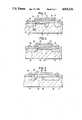
- FIG. 1is a cross-sectional view of a first embodiment of a punch-through injection type semiconductor non-volatile memory of the present invention
- FIG. 2is an explanatory view showing an energy band structure along the arrow A in FIG. 1;
- FIGS. 3 to 8are sectional views of other embodiments of a punch-through injection type semiconductor non-volatile memory of the present invention.
- FIG. 1is a sectional view of a first embodiment of a semiconductor non-volatile memory according the present invention.
- N + type source region 2, N + type drain region 3 and N + type carrier supply region 4(will be referred to as injector region hereinafter, N type is also usable for the injection region instead of N + type) are formed on the surface of a P type semiconductor substrate 1.
- a floating gate electrode 6 made of polycrystal siliconis provided, through a gate insulating film 5, on the surface of the semiconductor substrate 1 between the source region 2 and the drain region 3.
- a control gate electrode 8is formed on the floating gate electrode 6 through a gate insulating film 7. The control gate 8 is strongly coupled with the floating gate electrode 6 by capacitance coupling, and the control gate 8 serves to control the potential of the floating gate electrode 6.
- the floating gate electrode 6is formed over the drain region 3 and over an injection region 9 which is in contact with the drain region 3, through an insulating film 10.
- the carrier supply region 4, from which the injection carriers are supplied,is located at a position spaced apart from the injection region 9 by a distance LP.
- the reading out operation of a memory transistoris carried out by utilizing the fact that the threshold voltage of a channel region between the source and the drain regions for the control gate electrode 8 varies in accordance with the amount of charge on the floating gate electrode 6. That is, when a large number of electrons are injected in the floating gate electrode (in the case writing operation is made), the threshold voltage of the memory transistor is high. On the other hand, the threshold voltage is low for less electrons.
- the data in the memorycan be read out by detecting the channel conductance at the time a constant voltage is applied to the control gate electrode 8.
- FIG. 2is a view showing an energy band structure along the arrow A in FIG. 1.
- the surface potential of the injection region 9becomes low as shown in FIG. 2 due to the potential of the drain region 3 which is an injection region/potential control region and due to the potential of the control gate electrode 8.
- a space charge regionis formed due to the differences in respective potentials in a space charge forming region between the carrier supply region 4 and the injection region 9 formed on the semiconductor substrate. Consequently, as shown in FIG. 2, the potential of the space charge forming region in the region of the semiconductor substrate, which is shown by the solid line, lowers below the broken line, and electrons are accelerated and injected from the carrier supply region 4 to the floating gate electrode 6 in the direction of the arrow B.
- a feature of the present inventionresides in that electrons are injected from the carrier supply region 4 to the floating gate electrode 6 through an insulating film portion 10 of the gate insulating film 5 by lowering the potential in the space charge forming region on the semiconductor substrate 1 where the electrons are accelerated by the potential in the injection region 9.
- This injection methodis named "punch-through injection”.
- the punch-through injectionis an injection method in which the injection region and the substrate are not biased in the forward direction. Namely, the injection region 9 is biased in the forward direction with respect to the substrate 1 or the voltage of the injection region 9 is the same as the voltage of the substrate 1. As described herein, all of the voltage values are with respect to the voltage of the substrate 1.
- the punch-through injection according to the present inventionis a method in which charges from the carrier supply region 4 are accelerated to the floating gate electrode by lowering the potential of the space charge forming region on the semiconductor substrate 1 between the carrier supply region 4 and the injection region 9 without heightening the potential of the source region 2.
- the condition for the punch-through injectioncan be expressed as follows:
- V Aa difference in potential between the carrier supply region 4 and the injection region 9;
- 2 ⁇ .sub. ⁇ ; ⁇ .sub. ⁇is a Fermi level of the substrate 1 and the value of 2 ⁇ .sub. ⁇ is required as ⁇ for changing P type substrate to N type substrate.
- the punch-through injectionwill happen if the drain voltage and the control gate voltage are applied in such a way that V A is equal to 7 V.
- the distance lPis equal or less than 1 ⁇ m.
- the length of the distancecan be controlled by the use of the technique of fine fabrication, however, it can be controlled by the utilization of the side etching of the floating gate electrode 6 without high fine machining technique.
- a second control gate electrode 12is formed through a gate oxide film 13 on the semiconductor surface of the space charge forming region between the carrier supply region 4 and the injection region 9.
- the potential of the space charge forming regionis liable to be affected by the outer potential of the semiconductor surface, and to be unstable in the memory characteristics.
- the second control gate electrode 12 in the second embodiment of the present invention shown in FIG. 3is formed. With the second control gate electrode 12, the potential of the space charge forming region is controlled by only the voltages of the control gate electrode 8 and the drain region 3.
- the potential of the space charge forming regioncan be determined free from the outer potential of the semiconductor substrate surface, stable memory characteristics can be obtained.
- the maximum current pathor minimum current path
- the maximum current pathis not in the inversion layer of the semiconductor surface but in the inner or interior portion of the substrate.
- a carrier supply region 21acts as a source region of the memory transistor.
- a source region 21 and a drain region 22are formed on the surface of the semiconductor substrate 1
- a second control gate electrode 28 which is adjacent to the source region 21 and a floating gate electrode 29 which is adjacent to the drain region 22are formed on a channel region between the source and the drain regions, and furthermore, a control gate electrode 27 is formed on the floating gate electrode 29 through an insulation film 26.
- the channel region 25 under the floating gate electrode 29acts as an injection region.
- the channel region under the second control gate electrode 28is called the space charge forming region and this space charge forming region acts as the space change region when the carriers are injected into the floating gate electrode 29.
- the voltageis applied to the second control gate electrode 28 in such a way that the surface of the channel region under the gate insulation film 24 is sufficiently inverted.
- a constant voltageis applied to the control gate electrode 27, the channel conductance between the source and the drain regions varies in accordance with the amount of charges in the floating gate electrode 29. That is, the information in the floating gate electrode 29 is read out.
- the punch-through injectionis used in a manner similar to the second embodiment of the present invention shown in FIG. 3.
- the surface potential of the injection region 25is decreased by the potential of the drain region 22 and the potential of the control gate electrode 27.
- the potential of the space charge forming region between the source region 21 and the injection region 25is also decreased, and the electrons are accelerated from the source region 21 to the floating gate electrode 29 in the direction designated by arrow A. That is, the punch-through injection occurs.
- the accelerated electrons under the gate insulation film 24are accelerated not on the the substrate surface but through the inner portion of the substrate.
- FIG. 5a fourth embodiment of a semiconductor non-volatile memory of the present invention shown in FIG. 5 will be described.
- the drain region 22is able to act as the control gate electrode. That is, in order to control the potential of the floating gate electrode 29 by only the potential of the drain region 22, the degree of the capacitance coupling between the floating gate electrode 29 and the drain region 22 is set to be closer (as shown in FIG. 5, this can be realized by increasing the size of the overlap area of the floating gate electrode 29 and the drain region 22).
- the potential of the injection region 25is also determined by only the potential of the drain region 22.
- the reading-out operationis carried out by inverting the channel region under the gate insulation film 24 by the potential of the second control gate electrode 28, and detecting the channel conductance when a constant drain voltage having a predetermined level is applied to the drain region 22.
- the threshold voltage of the channel regionis large and the channel conductance is small.
- the channel conductanceis large for less electrons in the electrode 29.
- the writing operationis carried out by the punch-through injection which occurs at the portion between the source region 21 and the injection region 25.
- the potential of the injection region 25can be selected by the potential of the drain region 22.
- a charge supply regionis formed as shown in FIG. 6. That is, as shown in FIG. 6, a source region 21a which is able to act as a carrier supply region is formed just below the injection region 25. Therefore, the electrons are accelerated from the source region 21a to a floating gate electrode 29 along a straight line as shown by arrow C.
- the potential of the space charge forming region of the semiconductor substrate 1 which is between the source region 21a and the injection region 25becomes low with the lowering of the potential of the injection region 25, and the electrons are thus accelerated from the source region 21a to the injection region 25. That is, the punch-through injection occurs.
- the potential of the injection region 25is controllable by only the potential of the drain region 22.
- the reading-out operation of the memory transistoris the same as that of the fourth embodiment shown in FIG. 5.
- the sixth embodimentcomprises an N - type source region 38 which is able to act as a carrier supply region, a second control region 31, a drain region 32, an injection region 39, and a floating gate electrode 37 formed through an insulation film 36 on the surface channel region of a P type second control region 31 between the source-drain regions and the drain region 32.
- the reading-out operationcan be executed by utilizing the fact that the channel conductance of the channel region between the source regions depends on the amount of charge in the floating gate electrode.
- the potential of the injection region 39is lowered by the potentials of the drain region 32 and the second control region 31.
- the potential of the floating gate electrode 37increases by the voltage of the drain region 32, so that the channel region of the surface of the second control region 31 is inverted and lowers the potential of the injection region 39 toward the direction of the voltage of the drain region 32.
- the potential of the space charge region formed between the second control region 31is controlled so as to be at a low level by the potential of the injection region 39, and electrons are accelerated toward the floating gate electrode 37 as shown by the arrow D from the source region 38 which functions as the charge supply region. That is, the punch-through injection occurs.
- a control gate electrode 46 for a floating gate electrode 49is provided separately from a drain region 42 and, at the same time, the drain region 42 is provided so as to surround an injection region 47.
- the methods for reading out and writing inare approximately the same as those of the sixth embodiment.
- the writing-in operationcan be carried out effectively, and the reading-out operation can be also carried out by detecting the change in the conductance of the injection region due to the charge on the floating gate.
- the structureis suitable for formation by fine pattern techniques, it is suitable for a high density integrated memory.
- N type memory transistorsare described in the first through the seventh embodiments of the present invention.
- the present inventionis also applicable to P type memory transistors.
- the present inventioncan be realized by the use of a semiconductor layer formed on an insulation substrate.
- the selection of the writing of the memory cell of the present inventionbecomes possible by the control of the potential of the carrier supply region, the substrate, the control gate electrode or the second control gate electrode.
- the cell selection operationcan be carried out by applying the voltage to each electrode so as not to form a space charge region in the space charge forming region.
Landscapes
- Non-Volatile Memory (AREA)
- Static Random-Access Memory (AREA)
Abstract
Description
V.sub.A /lP·W.sub.P ≃Δφ≃2φ.sub.ƒ
Claims (5)
V.sub.A /l.sub.p ·W.sub.p ≃2φ.sub.f,
Applications Claiming Priority (2)
| Application Number | Priority Date | Filing Date | Title |
|---|---|---|---|
| JP58037172AJPS59161873A (en) | 1983-03-07 | 1983-03-07 | Semiconductor non-volatile memory |
| JP58-37172 | 1983-03-07 |
Related Parent Applications (1)
| Application Number | Title | Priority Date | Filing Date |
|---|---|---|---|
| US06587265Continuation | 1984-03-07 |
Publications (1)
| Publication Number | Publication Date |
|---|---|
| US4821236Atrue US4821236A (en) | 1989-04-11 |
Family
ID=12490173
Family Applications (1)
| Application Number | Title | Priority Date | Filing Date |
|---|---|---|---|
| US07/013,192Expired - LifetimeUS4821236A (en) | 1983-03-07 | 1987-02-09 | Semiconductor nonvolatile memory |
Country Status (2)
| Country | Link |
|---|---|
| US (1) | US4821236A (en) |
| JP (1) | JPS59161873A (en) |
Cited By (25)
| Publication number | Priority date | Publication date | Assignee | Title |
|---|---|---|---|---|
| US4982377A (en)* | 1988-12-27 | 1991-01-01 | Nec Corporation | Erasable programmable read only memory device improved in operation speed and in the amount of read out current |
| EP0399261A3 (en)* | 1989-05-24 | 1991-01-02 | Texas Instruments Incorporated | Band-to-band induced substrate hot electron injection |
| EP0501941A1 (en)* | 1991-01-31 | 1992-09-02 | Interuniversitair Microelektronica Centrum Vzw | Transistor structure for use in erasable and programmable semiconductor memory devices |
| EP0463331A3 (en)* | 1990-06-28 | 1992-12-23 | Texas Instruments Incorporated | An improved method for programming a non-volatile memory |
| EP0473129A3 (en)* | 1990-08-29 | 1993-02-03 | Texas Instruments Incorporated | Asymmetrical non-volatile memory cell, arrays and methods for fabricating same |
| US5216269A (en)* | 1989-03-31 | 1993-06-01 | U.S. Philips Corp. | Electrically-programmable semiconductor memories with buried injector region |
| EP0534676A3 (en)* | 1991-09-25 | 1993-09-15 | American Telephone And Telegraph Company | Eeprom with improved endurance properties |
| US5313421A (en)* | 1992-01-14 | 1994-05-17 | Sundisk Corporation | EEPROM with split gate source side injection |
| WO1996018998A1 (en)* | 1994-12-16 | 1996-06-20 | National Semiconductor Corporation | A method for programming a single eprom or flash memory cell to store multiple levels of data |
| WO1996031883A1 (en)* | 1995-04-06 | 1996-10-10 | National Semiconductor Corporation | A method for programming an amg eprom or flash memory when cells of the array are formed to store multiple bits of data |
| US5583810A (en)* | 1991-01-31 | 1996-12-10 | Interuniversitair Micro-Elektronica Centrum Vzw | Method for programming a semiconductor memory device |
| US5612914A (en)* | 1991-06-25 | 1997-03-18 | Texas Instruments Incorporated | Asymmetrical non-volatile memory cell, arrays and methods for fabricating same |
| US5712180A (en)* | 1992-01-14 | 1998-01-27 | Sundisk Corporation | EEPROM with split gate source side injection |
| US5808937A (en)* | 1994-12-16 | 1998-09-15 | National Semiconductor Corporation | Self-convergent method for programming FLASH and EEPROM memory cells that moves the threshold voltage from an erased threshold voltage range to one of a plurality of programmed threshold voltage ranges |
| US6009013A (en)* | 1992-01-29 | 1999-12-28 | Interuniversitair Micro-Elektronica Centrum Vzw | Contactless array configuration for semiconductor memories |
| US6222762B1 (en) | 1992-01-14 | 2001-04-24 | Sandisk Corporation | Multi-state memory |
| US6243293B1 (en) | 1992-01-29 | 2001-06-05 | Interuniversitair Micro-Elektronica Centrum | Contacted cell array configuration for erasable and programmable semiconductor memories |
| US20030052360A1 (en)* | 1992-01-14 | 2003-03-20 | Guterman Daniel C. | EEPROM with split gate source side injection with sidewall spacers |
| US20060062050A1 (en)* | 2004-09-21 | 2006-03-23 | Bohumil Lojek | Low voltage non-volatile memory cells using twin bit line current sensing |
| US20060060915A1 (en)* | 2004-09-21 | 2006-03-23 | Bohumil Lojek | Non-volatile nanocrystal memory transistors using low voltage impact ionization |
| US20060139998A1 (en)* | 2004-12-23 | 2006-06-29 | George Samachisa | Substrate electron injection techniques for programming non-volatile charge storage memory cells |
| US7092288B2 (en) | 2004-02-04 | 2006-08-15 | Atmel Corporation | Non-volatile memory array with simultaneous write and erase feature |
| US20140160868A1 (en)* | 2007-11-29 | 2014-06-12 | Zeno Semiconductor, Inc. | Method of Maintaining the State of Semiconductor Memory Having Electrically Floating Body Transistor |
| US10163907B2 (en) | 2008-09-03 | 2018-12-25 | Zeno Semiconductor, Inc. | Method of maintaining the state of semiconductor memory having electrically floating body transistor |
| US10340276B2 (en) | 2010-03-02 | 2019-07-02 | Zeno Semiconductor, Inc. | Method of maintaining the state of semiconductor memory having electrically floating body transistor |
Citations (5)
| Publication number | Priority date | Publication date | Assignee | Title |
|---|---|---|---|---|
| US4037242A (en)* | 1975-12-29 | 1977-07-19 | Texas Instruments Incorporated | Dual injector, floating gate MOS electrically alterable, non-volatile semiconductor memory device |
| US4163985A (en)* | 1977-09-30 | 1979-08-07 | The United States Of America As Represented By The Secretary Of The Air Force | Nonvolatile punch through memory cell with buried n+ region in channel |
| US4361847A (en)* | 1980-04-07 | 1982-11-30 | Eliyahou Harari | Non-volatile EPROM with enhanced drain overlap for increased efficiency |
| US4432075A (en)* | 1981-12-04 | 1984-02-14 | Hebrew University Of Jerusalem | Electrically programmable non-volatile memory |
| US4462090A (en)* | 1978-12-14 | 1984-07-24 | Tokyo Shibaura Denki Kabushiki Kaisha | Method of operating a semiconductor memory circuit |
- 1983
- 1983-03-07JPJP58037172Apatent/JPS59161873A/enactiveGranted
- 1987
- 1987-02-09USUS07/013,192patent/US4821236A/ennot_activeExpired - Lifetime
Patent Citations (5)
| Publication number | Priority date | Publication date | Assignee | Title |
|---|---|---|---|---|
| US4037242A (en)* | 1975-12-29 | 1977-07-19 | Texas Instruments Incorporated | Dual injector, floating gate MOS electrically alterable, non-volatile semiconductor memory device |
| US4163985A (en)* | 1977-09-30 | 1979-08-07 | The United States Of America As Represented By The Secretary Of The Air Force | Nonvolatile punch through memory cell with buried n+ region in channel |
| US4462090A (en)* | 1978-12-14 | 1984-07-24 | Tokyo Shibaura Denki Kabushiki Kaisha | Method of operating a semiconductor memory circuit |
| US4361847A (en)* | 1980-04-07 | 1982-11-30 | Eliyahou Harari | Non-volatile EPROM with enhanced drain overlap for increased efficiency |
| US4432075A (en)* | 1981-12-04 | 1984-02-14 | Hebrew University Of Jerusalem | Electrically programmable non-volatile memory |
Cited By (86)
| Publication number | Priority date | Publication date | Assignee | Title |
|---|---|---|---|---|
| US4982377A (en)* | 1988-12-27 | 1991-01-01 | Nec Corporation | Erasable programmable read only memory device improved in operation speed and in the amount of read out current |
| US5216269A (en)* | 1989-03-31 | 1993-06-01 | U.S. Philips Corp. | Electrically-programmable semiconductor memories with buried injector region |
| EP0399261A3 (en)* | 1989-05-24 | 1991-01-02 | Texas Instruments Incorporated | Band-to-band induced substrate hot electron injection |
| EP0463331A3 (en)* | 1990-06-28 | 1992-12-23 | Texas Instruments Incorporated | An improved method for programming a non-volatile memory |
| EP0473129A3 (en)* | 1990-08-29 | 1993-02-03 | Texas Instruments Incorporated | Asymmetrical non-volatile memory cell, arrays and methods for fabricating same |
| US5674764A (en)* | 1990-08-29 | 1997-10-07 | Texas Instruments Incorporated | Method of making asymmetric non-volatile memory cell |
| US5583811A (en)* | 1991-01-31 | 1996-12-10 | Interuniversitair Micro-Elektronica Centrum Vzw | Transistor structure for erasable and programmable semiconductor memory devices |
| EP0501941A1 (en)* | 1991-01-31 | 1992-09-02 | Interuniversitair Microelektronica Centrum Vzw | Transistor structure for use in erasable and programmable semiconductor memory devices |
| BE1004424A3 (en)* | 1991-01-31 | 1992-11-17 | Imec Inter Uni Micro Electr | TRANSISTOR STRUCTURE AND for erasable programmable memories. |
| US5583810A (en)* | 1991-01-31 | 1996-12-10 | Interuniversitair Micro-Elektronica Centrum Vzw | Method for programming a semiconductor memory device |
| US5612914A (en)* | 1991-06-25 | 1997-03-18 | Texas Instruments Incorporated | Asymmetrical non-volatile memory cell, arrays and methods for fabricating same |
| EP0534676A3 (en)* | 1991-09-25 | 1993-09-15 | American Telephone And Telegraph Company | Eeprom with improved endurance properties |
| US20030052360A1 (en)* | 1992-01-14 | 2003-03-20 | Guterman Daniel C. | EEPROM with split gate source side injection with sidewall spacers |
| US6275419B1 (en) | 1992-01-14 | 2001-08-14 | Sandisk Corporation | Multi-state memory |
| US6954381B2 (en) | 1992-01-14 | 2005-10-11 | Sandisk Corporation | EEPROM with split gate source side injection with sidewall spacers |
| US6856546B2 (en) | 1992-01-14 | 2005-02-15 | Sandisk Corporation | Multi-state memory |
| US5712180A (en)* | 1992-01-14 | 1998-01-27 | Sundisk Corporation | EEPROM with split gate source side injection |
| US5776810A (en)* | 1992-01-14 | 1998-07-07 | Sandisk Corporation | Method for forming EEPROM with split gate source side injection |
| US7898868B2 (en) | 1992-01-14 | 2011-03-01 | Sandisk Corporation | Multi-state memory |
| US5847996A (en)* | 1992-01-14 | 1998-12-08 | Sandisk Corporation | Eeprom with split gate source side injection |
| US5883409A (en)* | 1992-01-14 | 1999-03-16 | Sandisk Corporation | EEPROM with split gate source side injection |
| US5910915A (en)* | 1992-01-14 | 1999-06-08 | Sandisk Corporation | EEPROM with split gate source side injection |
| US5910925A (en)* | 1992-01-14 | 1999-06-08 | Sandisk Corporation | EEPROM with split gate source side injection |
| US6002152A (en)* | 1992-01-14 | 1999-12-14 | Sandisk Corporation | EEPROM with split gate source side injection with sidewall spacers |
| US5313421A (en)* | 1992-01-14 | 1994-05-17 | Sundisk Corporation | EEPROM with split gate source side injection |
| US6222762B1 (en) | 1992-01-14 | 2001-04-24 | Sandisk Corporation | Multi-state memory |
| US6317364B1 (en) | 1992-01-14 | 2001-11-13 | Sandisk Corporation | Multi-state memory |
| US6317363B1 (en) | 1992-01-14 | 2001-11-13 | Sandisk Corporation | Multi-state memory |
| US6243293B1 (en) | 1992-01-29 | 2001-06-05 | Interuniversitair Micro-Elektronica Centrum | Contacted cell array configuration for erasable and programmable semiconductor memories |
| US6009013A (en)* | 1992-01-29 | 1999-12-28 | Interuniversitair Micro-Elektronica Centrum Vzw | Contactless array configuration for semiconductor memories |
| US5594685A (en)* | 1994-12-16 | 1997-01-14 | National Semiconductor Corporation | Method for programming a single EPROM or flash memory cell to store multiple bits of data that utilizes a punchthrough current |
| US5808937A (en)* | 1994-12-16 | 1998-09-15 | National Semiconductor Corporation | Self-convergent method for programming FLASH and EEPROM memory cells that moves the threshold voltage from an erased threshold voltage range to one of a plurality of programmed threshold voltage ranges |
| WO1996018998A1 (en)* | 1994-12-16 | 1996-06-20 | National Semiconductor Corporation | A method for programming a single eprom or flash memory cell to store multiple levels of data |
| WO1996031883A1 (en)* | 1995-04-06 | 1996-10-10 | National Semiconductor Corporation | A method for programming an amg eprom or flash memory when cells of the array are formed to store multiple bits of data |
| US20040063283A1 (en)* | 1996-02-28 | 2004-04-01 | Guterman Daniel C. | Eeprom with split gate source side injection |
| US7449746B2 (en) | 1996-02-28 | 2008-11-11 | Sandisk Corporation | EEPROM with split gate source side injection |
| US20060163645A1 (en)* | 1996-02-28 | 2006-07-27 | Guterman Daniel C | EEPROM With Split Gate Source Side Injection |
| US7071060B1 (en) | 1996-02-28 | 2006-07-04 | Sandisk Corporation | EEPROM with split gate source side infection with sidewall spacers |
| US6704222B2 (en) | 1996-02-28 | 2004-03-09 | Sandisk Corporation | Multi-state operation of dual floating gate array |
| US6861700B2 (en) | 1996-02-28 | 2005-03-01 | Sandisk Corporation | Eeprom with split gate source side injection |
| US6664587B2 (en) | 1996-02-28 | 2003-12-16 | Sandisk Corporation | EEPROM cell array structure with specific floating gate shape |
| US6894926B2 (en) | 1997-08-07 | 2005-05-17 | Sandisk Corporation | Multi-state memory |
| US20080043529A1 (en)* | 1997-08-07 | 2008-02-21 | Guterman Daniel C | Novel Multi-State Memory |
| US6862218B2 (en) | 1997-08-07 | 2005-03-01 | Sandisk Corporation | Multi-state memory |
| US20060034124A1 (en)* | 1997-08-07 | 2006-02-16 | Sandisk Corporation | Novel multi-state memory |
| US20040042294A1 (en)* | 1997-08-07 | 2004-03-04 | Guterman Daniel C. | Novel Multi-state memory |
| US7573740B2 (en) | 1997-08-07 | 2009-08-11 | Sandisk Corporation | Multi-state memory |
| US7457162B2 (en) | 1997-08-07 | 2008-11-25 | Sandisk Corporation | Multi-state memory |
| US20060129751A1 (en)* | 1997-08-07 | 2006-06-15 | Guterman Daniel C | Novel multi-state memory |
| US20040165431A1 (en)* | 1997-08-07 | 2004-08-26 | Guterman Daniel C. | Novel multi-state memory |
| US20050002233A1 (en)* | 1997-08-07 | 2005-01-06 | Guterman Daniel C. | Novel multi-state memory |
| US20040246798A1 (en)* | 1997-08-07 | 2004-12-09 | Guterman Daniel C. | Novel multi-state memory |
| US7088615B2 (en) | 1997-08-07 | 2006-08-08 | Sandisk Corporation | Multi-state memory |
| US20050180211A1 (en)* | 1997-08-07 | 2005-08-18 | Guterman Daniel C. | Novel multi-state memory |
| US7443723B2 (en) | 1997-08-07 | 2008-10-28 | Sandisk Corporation | Multi-state memory |
| US7187592B2 (en) | 1997-08-07 | 2007-03-06 | Sandisk Corporation | Multi-state memory |
| US20080212374A1 (en)* | 1997-08-07 | 2008-09-04 | Guterman Daniel C | Novel Multi-State Memory |
| US7385843B2 (en) | 1997-08-07 | 2008-06-10 | Sandisk Corporation | Multi-state memory |
| US7289360B2 (en) | 1997-08-07 | 2007-10-30 | Sandisk Corporation | Multi-state memory |
| US7345934B2 (en) | 1997-08-07 | 2008-03-18 | Sandisk Corporation | Multi-state memory |
| US7092288B2 (en) | 2004-02-04 | 2006-08-15 | Atmel Corporation | Non-volatile memory array with simultaneous write and erase feature |
| US20060187707A1 (en)* | 2004-02-04 | 2006-08-24 | Atmel Corporation | Non-volatile memory array with simultaneous write and erase feature |
| US7301197B2 (en) | 2004-09-21 | 2007-11-27 | Atmel Corporation | Non-volatile nanocrystal memory transistors using low voltage impact ionization |
| US7020020B1 (en) | 2004-09-21 | 2006-03-28 | Atmel Corporation | Low voltage non-volatile memory cells using twin bit line current sensing |
| US20060060915A1 (en)* | 2004-09-21 | 2006-03-23 | Bohumil Lojek | Non-volatile nanocrystal memory transistors using low voltage impact ionization |
| US20060062050A1 (en)* | 2004-09-21 | 2006-03-23 | Bohumil Lojek | Low voltage non-volatile memory cells using twin bit line current sensing |
| US20070217264A1 (en)* | 2004-12-23 | 2007-09-20 | George Samachisa | Substrate Electron Injection Techniques for Programming Non-Volatile Charge Storage Memory Cells |
| US7230847B2 (en) | 2004-12-23 | 2007-06-12 | Sandisk Corporation | Substrate electron injection techniques for programming non-volatile charge storage memory cells |
| US7443736B2 (en) | 2004-12-23 | 2008-10-28 | Sandisk Corporation | Substrate electron injection techniques for programming non-volatile charge storage memory cells and for controlling program disturb |
| US20060139998A1 (en)* | 2004-12-23 | 2006-06-29 | George Samachisa | Substrate electron injection techniques for programming non-volatile charge storage memory cells |
| US9514803B2 (en) | 2007-11-29 | 2016-12-06 | Zeno Semiconductor, Inc. | Semiconductor memory having electrically floating body transistor |
| US8937834B2 (en)* | 2007-11-29 | 2015-01-20 | Zeno Semiconductor, Inc. | Method of maintaining the state of semiconductor memory having electrically floating body transistor |
| US9030872B2 (en) | 2007-11-29 | 2015-05-12 | Zeno Semiconductor, Inc. | Method of maintaining the state of semiconductor memory having electrically floating body transistor |
| US20140160868A1 (en)* | 2007-11-29 | 2014-06-12 | Zeno Semiconductor, Inc. | Method of Maintaining the State of Semiconductor Memory Having Electrically Floating Body Transistor |
| US9653467B2 (en) | 2007-11-29 | 2017-05-16 | Zeno Semiconductor, Inc. | Method of maintaining the state of semiconductor memory having electrically floating body transistor |
| US9793277B2 (en) | 2007-11-29 | 2017-10-17 | Zeno Semiconductor, Inc. | Method of maintaining the state of semiconductor memory having electrically floating body transistor |
| US10032776B2 (en) | 2007-11-29 | 2018-07-24 | Zeno Semiconductor, Inc. | Method of maintaining the state of semiconductor memory having electrically floating body transistor |
| US10163907B2 (en) | 2008-09-03 | 2018-12-25 | Zeno Semiconductor, Inc. | Method of maintaining the state of semiconductor memory having electrically floating body transistor |
| US10340276B2 (en) | 2010-03-02 | 2019-07-02 | Zeno Semiconductor, Inc. | Method of maintaining the state of semiconductor memory having electrically floating body transistor |
| US10453847B2 (en) | 2010-03-02 | 2019-10-22 | Zeno Semiconductor, Inc. | Method of maintaining the state of semiconductor memory having electrically floating body transistor |
| US10593675B2 (en) | 2010-03-02 | 2020-03-17 | Zeno Semiconductor, Inc. | Method of maintaining the state of semiconductor memory having electrically floating body transistor |
| US10748904B2 (en) | 2010-03-02 | 2020-08-18 | Zeno Semiconductor, Inc. | Method of maintaining the state of semiconductor memory having electrically floating body transistor |
| US11018136B2 (en) | 2010-03-02 | 2021-05-25 | Zeno Semiconductor, Inc. | Method of maintaining the state of semiconductor memory having electrically floating body transistor |
| US11183498B2 (en) | 2010-10-04 | 2021-11-23 | Zeno Semiconductor, Inc. | Semiconductor memory device having an electrically floating body transistor |
| US11737258B2 (en) | 2010-10-04 | 2023-08-22 | Zeno Semiconductor, Inc. | Semiconductor memory device having an electrically floating body transistor |
| US12185523B2 (en) | 2010-10-04 | 2024-12-31 | Zeno Semiconductor, Inc. | Semiconductor memory device having an electrically floating body transistor |
Also Published As
| Publication number | Publication date |
|---|---|
| JPS59161873A (en) | 1984-09-12 |
| JPH0481346B2 (en) | 1992-12-22 |
Similar Documents
| Publication | Publication Date | Title |
|---|---|---|
| US4821236A (en) | Semiconductor nonvolatile memory | |
| US5349221A (en) | Semiconductor memory device and method of reading out information for the same | |
| US4622656A (en) | Non-volatile semiconductor memory | |
| US4882707A (en) | Non-volatile semi-conductor memory device with double gate structure | |
| US6377490B1 (en) | Nonvolatile semiconductor memory device and method for driving the same | |
| US4495693A (en) | Method of integrating MOS devices of double and single gate structure | |
| US4616340A (en) | Non-volatile semiconductor memory | |
| US5079603A (en) | Semiconductor memory device | |
| KR100254006B1 (en) | Semiconductor memory device | |
| US4409723A (en) | Method of forming non-volatile EPROM and EEPROM with increased efficiency | |
| KR100887866B1 (en) | Silicon on insulator read-write non-volatile memory comprising lateral thyristor and trapping layer | |
| US4972371A (en) | Semiconductor memory device | |
| KR100712089B1 (en) | Semiconductor memory device and manufacturing method | |
| US5340760A (en) | Method of manufacturing EEPROM memory device | |
| US4794433A (en) | Non-volatile semiconductor memory with non-uniform gate insulator | |
| US4729115A (en) | Non-volatile dynamic random access memory cell | |
| US6509606B1 (en) | Single poly EPROM cell having smaller size and improved data retention compatible with advanced CMOS process | |
| US5189497A (en) | Semiconductor memory device | |
| US6335549B1 (en) | EEPROM with high channel hot carrier injection efficiency | |
| JPH0481347B2 (en) | ||
| US4224635A (en) | Dynamic storage element having static storage element behavior | |
| US5472891A (en) | Method of manufacturing a semiconductor device | |
| GB2151400A (en) | Non-volatile memories | |
| JPS5958868A (en) | Semiconductor non-volatile memory | |
| EP0259158A2 (en) | Semiconductor non-volatile random access memory |
Legal Events
| Date | Code | Title | Description |
|---|---|---|---|
| AS | Assignment | Owner name:KOGYO GIZYUTSUIN, 3-1, KASUMIGASEKI 1-CHOME, CHIYO Free format text:ASSIGNMENT OF ASSIGNORS INTEREST.;ASSIGNORS:HAYASHI, YUTAKA;KOJIMA, YOSHIKAZU;TANAKA, KOJIRO;REEL/FRAME:004823/0267 Effective date:19871225 Owner name:SEIKI INSTRUMENTS & ELECTRONICS LTD., 31-1, KAMEID Free format text:ASSIGNMENT OF ASSIGNORS INTEREST.;ASSIGNORS:HAYASHI, YUTAKA;KOJIMA, YOSHIKAZU;TANAKA, KOJIRO;REEL/FRAME:004823/0267 Effective date:19871225 Owner name:KOGYO GIZYUTSUIN,JAPAN Free format text:ASSIGNMENT OF ASSIGNORS INTEREST;ASSIGNORS:HAYASHI, YUTAKA;KOJIMA, YOSHIKAZU;TANAKA, KOJIRO;REEL/FRAME:004823/0267 Effective date:19871225 Owner name:SEIKI INSTRUMENTS & ELECTRONICS LTD.,JAPAN Free format text:ASSIGNMENT OF ASSIGNORS INTEREST;ASSIGNORS:HAYASHI, YUTAKA;KOJIMA, YOSHIKAZU;TANAKA, KOJIRO;REEL/FRAME:004823/0267 Effective date:19871225 | |
| STCF | Information on status: patent grant | Free format text:PATENTED CASE | |
| FPAY | Fee payment | Year of fee payment:4 | |
| FPAY | Fee payment | Year of fee payment:8 | |
| FPAY | Fee payment | Year of fee payment:12 |