US4821170A - Input/output system for multiprocessors - Google Patents
Input/output system for multiprocessorsDownload PDFInfo
- Publication number
- US4821170A US4821170AUS07/040,513US4051387AUS4821170AUS 4821170 AUS4821170 AUS 4821170AUS 4051387 AUS4051387 AUS 4051387AUS 4821170 AUS4821170 AUS 4821170A
- Authority
- US
- United States
- Prior art keywords
- bus
- controller
- input
- channel
- data
- Prior art date
- Legal status (The legal status is an assumption and is not a legal conclusion. Google has not performed a legal analysis and makes no representation as to the accuracy of the status listed.)
- Expired - Lifetime
Links
Images


Classifications
- G—PHYSICS
- G06—COMPUTING OR CALCULATING; COUNTING
- G06F—ELECTRIC DIGITAL DATA PROCESSING
- G06F13/00—Interconnection of, or transfer of information or other signals between, memories, input/output devices or central processing units
- G06F13/14—Handling requests for interconnection or transfer
- G06F13/20—Handling requests for interconnection or transfer for access to input/output bus
- G06F13/28—Handling requests for interconnection or transfer for access to input/output bus using burst mode transfer, e.g. direct memory access DMA, cycle steal
- G—PHYSICS
- G06—COMPUTING OR CALCULATING; COUNTING
- G06F—ELECTRIC DIGITAL DATA PROCESSING
- G06F13/00—Interconnection of, or transfer of information or other signals between, memories, input/output devices or central processing units
- G06F13/10—Program control for peripheral devices
- G06F13/12—Program control for peripheral devices using hardware independent of the central processor, e.g. channel or peripheral processor
- G06F13/122—Program control for peripheral devices using hardware independent of the central processor, e.g. channel or peripheral processor where hardware performs an I/O function other than control of data transfer
- G—PHYSICS
- G06—COMPUTING OR CALCULATING; COUNTING
- G06F—ELECTRIC DIGITAL DATA PROCESSING
- G06F13/00—Interconnection of, or transfer of information or other signals between, memories, input/output devices or central processing units
- G06F13/38—Information transfer, e.g. on bus
- G06F13/40—Bus structure
- G06F13/4004—Coupling between buses
- G06F13/4022—Coupling between buses using switching circuits, e.g. switching matrix, connection or expansion network
- G—PHYSICS
- G06—COMPUTING OR CALCULATING; COUNTING
- G06F—ELECTRIC DIGITAL DATA PROCESSING
- G06F11/00—Error detection; Error correction; Monitoring
- G06F11/07—Responding to the occurrence of a fault, e.g. fault tolerance
- G06F11/08—Error detection or correction by redundancy in data representation, e.g. by using checking codes
- G06F11/10—Adding special bits or symbols to the coded information, e.g. parity check, casting out 9's or 11's
Definitions
- the present inventionrelates generally to communication between a plurality of digital processors in a multiprocessor-based computer system and peripheral devices, such as disk drives and tape drives, which operate at disparate speeds. More particularly the invention relates to an architecture for communicating between two independently-operating ports and peripheral devices coupled to a version of the Small Computer System Interface (SCSI).
- SCSISmall Computer System Interface
- processorsSeveral classes of digital computer systems use a plurality of independent processors to perform computer operations. Examples include fault-tolerant, modular and parallel processing systems. These processors, herein referred to as host processors, require digital data exchange (input and output) with other devices, known as peripherals.
- a system busunder the supervision of a bus controller.
- Information exchanged with the peripheral devicesis typically under the supervision of an input/output subsystem called a device controller.
- a device controllerwhich facilitates exchange of high speed, essentially synchronously-communicated data with relative low-speed, essentially asynchronous peripheral devices.
- the device controlleris constructed to insure that no single host processor failure can impair system operation.
- the device controller in the Katzman et al. patentis constructed with the intention of handling exchange of data at relatively high data rates as far as the host processor is concerned in order to minimize interference with programs running in the host processors.
- the device controlleris an interrupt-driven system and provides an input/output program interrupt (IO interrupt) only upon completion of a data transfer in order to relieve the host processor of the burden of being dedicated to the peripheral device during data transfer.
- IO interruptinput/output program interrupt
- the device controllerhas multiple ports, each of which is logically and physically independent of all other ports so that each device controller can be connected for access to at least two different host processors.
- the device controller of the computing system disclosed in the Katzman et al. patentemploys a microprocessor which is dedicated to input/output operations (I/O MPU).
- the I/O MPUcontrols an input/output bus structure internal to the device controller (device controller bus structure) over which is carried all data from any requesting host processor and any responding peripheral device as well as data intended solely for its own operation and control of commands. It is through this internal bus structure that the host processor informs the I/O MPU of data transfer type, requested peripheral device, data block size, priority and the like. It is also through the I/O MPU and the device controller bus structure that "ownership" of the operation of the device controller is effected.
- the device controlleris constructed to grant "sole ownership" to only one host processor at a time through a switching scheme which selects among ports of the device controller.
- there are only two ports and only one ownership latchwhich grants ownership to either a first port or a second port and hence only one channel I/O bus.
- only one peripheralcan be used by a host processor, and only one host processor can have access to any peripheral through the device controller when but a single port is in use and in the process of exchanging data. Access to the device controller from other host processors must thereafter be made through the host processor having ownership of the device controller. This represents a serious shortcoming when several peripheral devices are coupled through a single device controller and several host processors desire access to those pheripheral devices.
- Another shortcoming of the device controller in accordance with the invention disclosed in the Katzman et al. patentis the limited ability to connect the device controller with large numbers of peripheral devices or peripheral devices having an interconnection structure of selected types which have been widely accepted as standards.
- peripheral device typesWith the proliferation of peripheral device types, it is no longer feasible to construct a dedicated interface for each type or brand of peripheral device, each with its unique requirements and characteristics. This is particularly true at the growing "low end" of the computer market, where systems once costing hundreds of thousands of dollars are being superseded by system costing only a fraction of its predecessor.
- One reasonhas been standardization, which creates economies of scale.
- an input/output systemwhereby ownership of the input/output channels is shared.
- the device controllerincludes a first port controller having a first ownership latch, a second port controller having a second ownership latch, a first bus, a dedicated microprocessor having control over the first bus (the MPU bus), a second, higher-speed bus, a multiple-channel direct memory access (DMA) controller which is an extremely fast state machine, which controls the second bus (the data buffer bus) and access to the input/output ports, a bus switch whereby data communicated between devices on the MPU bus and devices on the data buffer bus are exchanged efficiently, a multiple port peripheral device interface, such as a Small Computer System Interface (SCSI), and at least provision for interface with data communication equipment (DCEs) or data terminal equipment (DTEs).
- SCSISmall Computer System Interface
- DCEsdata communication equipment
- DTEsdata terminal equipment
- the data buffer busoperates in a synchronous manner.
- the DMAprovides dynamic arbitration of the use of channels of the DMA.
- the DMAallocates alternate bus clock cycles in response to requests to exchange data.
- the microprocessoris allowed access to the data buffer bus only if the data buffer bus is not in use for data transfer.
- the data buffer bushas coupled to it all input/output ports to the system bus, the DMA controller, a high-speed buffer memory, the bus switch, and a multiplexed SCSI controller
- the MPU bushas coupled to its a microprocessor, program memory, data memory, command registers, communications devices (such as interfaces for data terminal equipment and data communication equipment), and the bus switch. All data is routed through the data buffer bus.
- the microprocessorconfigures the SCSI controller and the DMA controller for the type of data exchange.
- the latches associated with each portgrant ownership to either port or all ports allowing data exchange between addressed peripheral devices and requesting ports. Ownership is not surrendered so long as a host processor has need of a device controller.
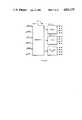
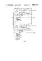
- FIG. 1is a block diagram view of a multiprocessor system constructed in accordance with one embodiment of the present invention, including a plurality of dual-port device controllers sharing peripheral devices coupled to Small Computer System Interface buses.
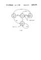
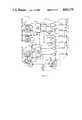
- FIG. 2is a simplified block diagram of one embodiment of a device controller according to the invention illustrating a direct memory access controller, a data buffer bus, a microprocessor bus, a bus switch and two SCSI buses.
- FIG. 3is a simplified block diagram of one embodiment of a dual-channel DMA controller.
- FIG. 4is simplified state diagram of operation of one embodiment of a dual-channel DMA controller.
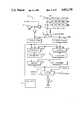
- FIG. 5shows the orientation of 5A and 5B which together form a block diagram of the architecture of a specific embodiment of a dual-channel DMA controller.
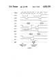
- FIG. 6is a timing diagram illustrating one type of operation of a specific embodiment of a dual-channel DMA controller.
- FIG. 7is a block diagram of a specific embodiment of two peripheral port controllers according to a specific embodiment of the invention.
- FIG. 8is a block diagram of a specific embodiment of a Small Computer System Interface controller according to the invention.
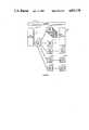
- FIG. 9is a block diagram illustrating a specific embodiment of the relationship between software modules according to the invention.
- FIG. 10is a block diagram illustrating a specific embodiment of calling protocols between software modules according to the invention.
- FIG. 11is a block diagram of a bus switch in accordance with a specific embodiment of the invention.
- FIG. 1For an overview of a specific embodiment of the invention.
- host processors 33also designated 33-0 and 33-1
- IPBsinterprocessor buses
- IPB-XX bus
- IPB-YY bus
- Each bus 35is controlled by a bus controller 37.
- Each host processor 33is provided with an input/output channel (I/O channel) 109 (designated 109-0 and 109-1) coupled to a channel I/O bus (CIO bus) 39 (designated 39-0 and 39-1).
- I/O channelinput/output channel
- CIO buschannel I/O bus
- FIG. 1also shows a plurality of device controllers 41 (designated 41-0 and 41-1) connected in accordance with the invention.
- the CIO bus 39 of each host processor 33is coupled to preferably at least one port of each device controller 41, and more specifically, first CIO bus 39-0 is connected to a first peripheral port controller (PPC-0) 43-0 of each device controller 41-0 and 41-1 and second CIO bus 39-1 is coupled to a second peripheral port controller (PPC-1) 43-1 of a each device controller 41-0 and 41-1.
- PPC-0peripheral port controller
- PPC-1second peripheral port controller
- the device controller 41is provided with a protocol controllers (SPC) 44 for two peripheral device buses 111 of a standardized configuration known as the Small Computer System Interface (SCSI), designated herein SCSI-0 111-0 and SCSI-1 111-1.
- SCSISmall Computer System Interface
- the SCSI standardhas been described in publications by the American National Standards Institute as ANSI Standard X3.131-1986, and commercial component parts are available for implementing functions of the SCSI bus.
- the SCSI interfaceis implemented by a type MB87030 chip made by Fujitsu and available from Fujitsu America of Santa Clara, Calif.
- the primary function of the SCSI buses 111is to provide port connections for standard SCSI peripherals, such as a tape drive 49 (with internal SCSI controllers) and disk drives 45 (with internal SCSI controllers).
- the SCSI busis of a type which allows more than one device controller to be connected thereto. (For example, up to eight units or devices, including device controllers, can be connected to a single SCSI bus.)
- both the first device controller 41-0 and the second device controller 41-1are connected to the first SCSI bus 111-0, the first SCSI bus 111-0 having connected thereto a first set of SCSI peripheral devices 45 and 49.
- each CIO bus 39has at least two paths to each SCSI device 45 or 49, and each host processor has at least four paths (two through another host processor via an IPB 35) to each SCSI device 45 or 49.
- This configurationsubstantially enhances the reliability of the overall computer system and permits the temporary removal for example of one device controller without compromising access to any other of the SCSI devices.
- the device controllers 41may also provide for access to or from the host processors 33 for asynchronous terminals 47 and packetized communication links 347 including links conforming to the ANSI protocol standards X.25 or X.21.
- FIG. 1The configuration and computer architecture represented by FIG. 1 is a new type of system representing a departure and enhancement over the structure disclosed in the Katzman et al. patent, incorporated herein by reference.
- DB busdata buffer bus
- MPU busmicroprocessor bus
- DBBSfirst bus switch
- the DB bus 100is a synchronous bus whose operational clock rate is a substantially different rate than the MPU bus 102
- DBBS 104is a bus switch which buffers transfers of data and commands between the DB bus 100 and the MPU bus 102 to assure timely transfer of data and commands between the buses operating at disparate clock rates.
- Coupled to the BS bus 100are a data buffer direct memory access controllers (DB DMA) 106, the first PPC 43-0, the second PPC 43-1, the SPC 44 and a high speed read/write random access memory (DB MEM) 108 for temporary storage of all data-type information transferred over the DB bus 100.
- DB DMAdata buffer direct memory access controllers
- DB MEMhigh speed read/write random access memory
- MPUmicroprocessor
- EEROMElectronically Erasable Read Only Memory
- MEMrandom access memory
- DMAdirect memory access controller
- SCCstandard serial communication chip device
- DUARTdual universal asynchronous receiver-transmitter
- the DMA 114is used to transfer data to and from the SCC 116 or the DUARTs 118 and the MEM 112 on the MPU bus. It cooperates closely with the MPU 119. DMA 114 channels can be programmed to move large data blocks and generate an interrupt signal to the MPU 119 at the end of a transmission.
- the SPC 44has two ports 144-0 and 144-1 for SCSI buses 111-0 and 111-1.
- the SCSI busesare multiplexed.
- an SPC bus 120is provided as part of the SPC configuration together with SPC bus switch 122, which provides bi-directional command and control coupling between the MPU bus 102 and the SPC bus 120.
- the device controller 41generates or responds to a plurality of interrupts on interrupt lines (not shown for clarity).
- the interruptsare generated by I/O channels through the PPCs 43, by I/O devices through the SPC 44, by DMA channels from the DB DMA 106 or DMA 114, by communication interfaces such as the SCC 116 and the DUARTs 118, by timeouts and by hardward errors.
- the interrupt issued by the PPCs 43in response to an EIO from a host processor.
- the DB DMA 106is a very fast state machine whose function is to control access to the DB bus 100.
- the DB DMA 106employs a technique known as dynamic arbitration to allocate time for data transfer on the DB bus 100 between the PPCs 43 and the peripheral devices through the SPC 44.
- the DB DMA 106includes arbitration logic 200 for allocating time on the DB bus 100 (FIG. 2) between two channels of data transfer functions as well as device controller management functions carried out under control of the MPU 119, all of which require usage of the DB bus 100.
- the DB DMA 106is a dual channel device which is capable of concurrent support for two channels of data, of being reprogrammed to support chaining of consecutive frames of data without having to repeat an interrupt cycle for each frame of data, and of being reprogrammed to support data transfer at twice the standard rate by use of both channels for a single task.
- the arbitration logicis responsive to the following requests: Request for Channel 0 (REQO*) (the * is used to denote logic LOW is TRUE), Request for Channel 1 (REQ1*), and bus request for the MPU 119 (BREQ*).
- the DB DMAissues at least the following interrupts: Acknowledge availability of Channel O (ACKO*), Acknowledge availability of Channel 1 (ACK1*), Bus usage granted in response to BREQ* (BGNT*).
- SYSCLKsystem clock
- XFRO and XFR1two-channel data transfer
- the maximum latency (210 FIG. 6) from DMA Request to DMA Acknowledgeis two clock cycles for either channel of the DB bus 100.
- the latency time for a bus requestdepends on the load on the channels. There may be a timeout provided for example. In the extreme, the latency time can be no longer than the time required to exhaust the queue of outstanding channel requests, since all channel requests are generated by the MPU 119.
- the arbitration logicis in communication with three substantially identical state machines, a channel 0 state machine (CHO SM) 202, a channel 1 state machine (CH1 SM) 204 and a bus request/bus grant state machine (BREQ/BGNT SM) 206.
- Each of the state machines 202, 204, 206is substantially identical in that each has four states S0, S1, S2, S3 as represented in FIG. 4.
- State S0is the idle state
- state S1is the acknowledge state following any request made (REQ0, REQ1, BREQ) during the idle state
- state 2is a data transfer state
- state 3is the error state.
- State S1is the Acknowledge state, meaning that the state machine expects a certain sequence of signals following issuance of an acknowledgement to the requesting element. Specifically, continued assertion of a Request signal (REQ*) and transfer of data is expected following state S1; otherwise an error condition is indicated (state S3). The state machine transitions between state S1 and state S2 until all data transfer is complete and the Request signal is withdrawn (REQ* disasserted). When in state S1 REQ* is disasserted, the state machine transitions to the Error state S3. It remains in the "Error” state until assertion of the Reset signal. When the Reset* signal is asserted in the Error state, the state machine is restored to the Idle state S0.
- Each of the channels for data transfer(XFRO and XFR1 of FIG. 6 referring to CH0 and CH1, respectively) operate independently of one another but of course cannot, during the same bus cycle, transfer data between the same peripheral device through the SPC 44 and the same requesting port PPC-0 43-0 or PPC-1 43-1. Every normal data transfer is written to or read out of a memory location in the DB MEM 108 which has been designated by the memory address output (MADRS) 224 of the DB DMA (FIG. 5).
- MADRSmemory address output
- FIG. 5there is shown a diagram of the architecture of the DB DMA 106.
- a key feature of the architectureis a fast adder or more specifically a two level Carry Look Ahead (CLA) adder which is capable of doing add and subtract operations for the channel address generation in less than one clock period.
- CLACarry Look Ahead
- the contents of channel 0 and channel 1 address registers 216 and 218are provided as one input to the CLA adder 214 via an address multiplexer ADRS MUX 220.
- the augend address (ADRS AUGEND) 222is provided as the other input to CLA adder 214, the output of which is the memory address (MADRS) in the DB MEM 108 to or from which the data on the DB bus 100 is written or read.
- the DB DMA 108is capable of chaining related data in a block for continuous transfer of priority data at the designated standard data transfer rate. This is a function which would normally be carried out by the MPU 119 (FIG. 2) and would require that an interrupt cycle be repeated for each frame of data. However, the DB DMA 106 according to the invention is instead employed for this purpose. The result is a substantial increase in speed of selected data transfer operations of the device controller 41.
- a Master Control register 260, a Channel 0 control register 262, and a Channel 1 control register 264are coupled to receive input data via a register bus 266 from a data input/output port 268 and further to provide output to a the register bus 266 and the data input/output port 268 via a register multiplexer 270. Further as shown in FIG. 5,
- a Channel 0 chain pointer register CHO CHAIN PTR REG 226is coupled to Channel 0 address multiplexer 228 to the Channel 0 address register CHO ADR REG 216
- Channel 1 chain pointer register CH1 CHAIN PTR REG 230is coupled to Channel 1 address multiplexer 232 to the Channel 1 address register CH1 ADR REG 218.
- the chaining functionis enabled by placement of a suitable command word in the channel control register 262. Once chaining has been enabled, the respective channel address registers 216 and 218 of the enabled channel are loaded from the corresponding channel chain pointer register 226 or 228, so that chained sequencing is started. Chained sequencing continues until chain parameters are fetched from memory; thereafter regular channel operation resumes.
- the ability to reprogram a channel of DB DMA 106 for chaining operations while supporting normal functions on other channelsrepresents a departure from known technology in this field.
- a comparator 250is provided for comparing the content of the active channel address register 216 or 218 via the address MUX 220 with the content of the corresponding end pointer register 254 or 256 via an end address multiplexer (END-ADRS-MUX) 258.
- the output of the comparator 250is either an Equal or NOT Equal value, which is used to control data transfer.
- Another feature of the inventionis the use of address parity prediction to assure that the system is operating properly. More specifically, address parity of the next scheduled address is predicted and compared with actual parity to assure that data is actually being progressively transferred to and from the proper memory locations.
- a conventional parity generator 270is provided having as its input the output of the CLA adder 214, a parity predictor 272 having as its input the output of the channel address register 216 or 218 via the output of the address multiplexer 220 and as its other input selelected control bits of the corresponding channel control register 262 and 264 via the multiplexer 270 through register bus 266.
- the outputs of the parity generator 270 and the parity predictor 272are coupled to a comparator 274.
- the channel control register 262, 264contains information regarding the type of transfer and the address increment for each channel.
- the channel address register 216, 218contains the current address of each channel.
- the parity predictor 272comprises means for combining the address increment and the current address to obtain a predicted parity.
- the output of the comparator 274is thus an indication of whether the current parity and the parity predicted from the previous address. Inequality is an error condition.
- FIG. 7is a block diagram of a specific embodiment of two peripheral port controllers (PPCs) 43-0 and 43-1 according to a specific embodiment of the invention.
- PPCsperipheral port controllers
- each PPC 43includes a port chip 302-0, 302-1 coupled to a data buffer 303-0, 303-1 whereby EIOs issued on the CIOs 39-0, 30-1 cause interrupts and set the PPC latches 300-0, 300-1.
- the port chips 302-0, 302-1also provide limited data buffering between the CIOs 39-0, 39-1 and the DB bus 100.
- Each PPC 43has the following registers for receiving EIOs and data buffering:
- Buffer -- Aa data buffer
- Buffer -- Ba data buffer
- Buffer -- Ca data buffer
- RISTregister for storage of the Read Interrupt STatus word of an interrupt sequence
- LACregister for storage of the Load Address and Command word of an EIO sequence
- LPRMregister for storage of the Load PaRameter word of an EIO sequence
- Burst Lengthregister controlling the maximum number of word in a single reconnect burst (maximum 128).
- the DB DMA 106has direct access to the three Buffers A, B and C for both read access and write access. These buffers are word-wise registers configured in a bidirectional queue. These registers are clocked by the system clock (SYS -- CLK) (associated with the host processors) during transfers in from the DB bus 100 to the CIO 39. During out transfers they are clocked by the CIO 39 channel handshake signal SVO (see the Katzman et al. patent for further explanation of the CIO 39). Two three-bit circular shift registers are used as pointers. The first pointer is clocked by SYS -- CLK, and the shift is enabled by the DMA -- ACK signal from DB DMA 106 (FIG. 6).
- SYS -- CLKsystem clock
- SVOchannel handshake signal
- the second pointeris clocked by SVO, and shift is enabled by an IN or OUT TBUS command through the CIO 39.
- the two pointerskeep track of the next register (Buffer A, B, or C) to be loaded with data or unloaded.
- Buffer A, B, or CAt two-bit synchronous counter keeps track of the number of words in the buffers A, B, and C. The synchronous count is used to determine when the DMA -- REQ* signal must be asserted, and it is available to the MPU 119 via the status registers.
- the PPC latches 300do not assert a "Port Own” signal (PO -- OWN* by PPC latch 300-0 and P1 -- OWN* by PPC latch 300-1). However, whenever the appropriate EIO is received by the PPC chip 302, a "take ownership” interrupt signal is asserted (Takedown*) by the PPC chip 302 to the PPC latch 300 via signal line 304. Each PPC port 41 is properly identified via comparators 306 and appropriate switches 308. The addressed PPC latch 300 asserts port ownership (PO -- OWN* and P1 -- OWN*) as interrupts to the MPU 119.
- the MPU 119interprets the EIO, to designate which of the ports is to have which data channel of the DB bus 100 and to configure the DB DMA 108 to so allocate the two data channels CHO and CH1 of the DB bus 100 to one or both of the designated ports.
- the device controllercan handle all of the protocols and data transfers to and from peripheral devices within a common time frame and as far as the CIO buses 39 are concerned, simultaneously.
- Each PPC 43is capable of essentially simultaneous operation. In simultaneous operation, a first PPC 43-0 can actively transfer data and commands while the second PPC 43-1 can also actively transfer information; however such transfer is limited to commands.
- the DB DMA 106In the process of receiving an EIO, the DB DMA 106 must grant bus access to the MPU 119. To this end, the MPU 119 responds to the appropriate interrupt issued by the PPC 43 by issuing a BRQT signal to the DB DMA 106 via the bus switch 104.
- the bus switch 104comprises a three-state buffer 400, a delay means 402 and a latch 404.
- the output enable terminal of the three state buffer 400is controlled from the DB DMA 106 (a clock line synchronized with the channel in use) through the delay means 402 whose function is to enable the three-state buffer 400 after sufficient time has elapsed following a prior transfer of data to minimize interference between consecutive data blocks from the MPU bus 102 to be transferred to the higher speed DB DMA bus 100.
- the delay means 402typically provides a 20 ns delay and therefore a 20 ns window between data transfers between data transfers operating on a 200 ns clock.
- the bus switch 104further comprises a latch 404 which is coupled to receive data from the higher speed DB bus 100. It operates to latch the received data for use by the slower MPU bus 102.
- the latch 404is also a three state device wherein the output enable terminal is under control of the MPU 119, since the MPU 119 decides when to read the contents of the latch 404.
- operational control of the bus switch 104resides in the DB DMA 106, and more particularly is part of the arbitration logic 200 and Bus Request/Bus Grant protocol of the BREQ/BGNT state machine 206 for communication with MPU 119 and any other element coupled to the MPU bus 102. (Most data transfer for example is via the memory 112 under control of the 68450 DMA 114.) Operation of the bus switch 104 in conjunction with the MPU 119 is illustrated by the following example.
- the transfer of the EIO to the MPU 119is from the PPC 43 through the bus switch 104 to the MPU 119.
- the PPC 43issues an interrupt to the MPU 119 which in turn initiates a Bus Request to the DB DMA 106.
- the DB DMA 106then issues a Bus Grant to the MPU 119.
- the MPU 119then captures the EIO from the PPC 43 via the DB bus 100 and the bus switch 104.
- the MPU 119interprets the command structure while the DB DMA 106 controls other data transfers on the DB bus 100.
- Once the MPU 119 has completed interpretation of the EIOit again requests a bus cycle of the DB bus to access the DB DMA 106 to instruct it regarding the port and from of data transfer.
- a Bus Grantis given the MPU 119 transfers instructions to the registers of the DB DMA 106 via the bus switch 104.
- bus switcheswhich comprises buffers and latches
- different speed devicescan be interfaced very easily and even changed if necessary. For example, if it is desired to substitute a faster microprocessor chip in the position of MPU 119, it becomes the relatively trivial task of exchanging components and boosting MPU bus clock speed. The speed and operation of the DB bus 100 is not affected.
- the MPU 119accesses the SPC 44 via the SPC bus switch 122 and SPC bus 120 in order to configure the SPC 44 for the data transfer designated by the EIO and related vectors.
- the SPC 44is built around a SCSI Protocol Controller Chip (SPC Chip) 402 which in a specific embodiment may be a type MB87030 supplied by Fujitsu.
- SPC Chip 44is coupled indirectly to the DB bus 100 and directly to the SPC bus 120.
- Coupled between the DB bus 100 and the SPC chip 402is a byte assembly register 404 on the DB bus 100, which assembles the data bytes for the SPC Chip 402 to be passed via lines 403, and a parity register 406 which creates odd parity for data in the byte assembly register 404 to provide compatibility with the parity expected by the SPC Chip 402.
- the SPC bus switch 122comprises a latch 410 and a buffer 412. It is coupled between the MPU bus 102 and the SPC bus 120 to provide bi-directional command and control coupling between the MPU bus 102 and the SPC bus 120.
- the SPC bus switch 122is enabled by a signal on interrupt line 408 from the MPU 119 to latch 410 and buffer 412.
- SPC Chip 402Since the SPC chip 402 has only one SCSI port, provision must be made according to the invention to connect two SCSI buses 111-0 and 111-1. Therefore SPC Chip 402 provides a set of driver lines 414 and receiver lines 416 to a multiplexer set 418.
- the multiplexer set 418 for the SPC Chip 402itself comprises first and second sets of dual input open collector output NAND gates 420-0 and 420-1 which are functional as enablable drivers for SCSI bus 0 111-0 and SCSI bus 1 111-1, respectively, and corresponding first and second sets of inverters 420-0 and 420-1, which are functional as three-state receivers for SCSI bus 0 111-0 and SCSI bus 1 111-1, respectively.
- third and fourth inverter sets 424-0 and 424-1are coupled as receivers from the respective SCSI buses 111-0 and 111-1 and supplied to SCSI interrupt logic means 426, which is coupled to the SPC bus 120 and which has interrupt line 428 which is coupled to the MPU 119.
- a bus select register 430is provided on the SPC bus 120 which has an outputs an Enable Bus 0 line 432 and an Enable Bus 1 line 434.
- Enable Bus 0 line 432is coupled to drivers 420-0 and receivers 422-0 associated with SCSI bus 0 111-0
- Enable Bus 1 line 434is coupled to drivers 420-1 and receivers 422-1 associated with SCSI bus 1 111-1.
- the SPC 41can respond with programming commands from the MPU 119 via the SPC bus 102 directed to the SPC Chip 402, can pass data (read and write) to/from the DB bus 100 from/to either SCSI bus 111-0 or 111-1 as selected by a command from the MPU 119 via the bus select register means 432, or it can interrupt the MPU 119 via interrupt line 428 from the SCSI interrupt logic means responsive to signals from peripheral devices on either SCSI bus 111-0 or 111-1.
- the device controller 41permits multiple access from multiple channels to multiple devices on selectable SCSI buses within the same operational cycle, during two or more overlapping commands.
- the byte assembly register 404can be read and written in word mode by the MPU 119 via the DB bus 100. This facilitates data transfer between an eight bit device (the SPC Chip 402) and a high speed sixteen bit bus (DB bus 100). Specifically, during IN mode transfers from the SPC Chip 402, the first byte to the DB bus 100 is stored in the most significant byte side of the byte assembly register 404 and when the second byte is ready, the first byte is passed from the byte assembly register 404 to the most significant byte side of the DB bus 100 while the least significant byte is passed via three state driver 405 to the least significant byte side of the DB bus 100.
- the least significant byte of the DB bus 100is transferred to the least significant byte side of the byte assembly register 404 as the most significant byte of the DB bus 100 is transferred directly to the the SPC through three state driver 407.
- the next byte transferred to the SPC Chip 402is the least significant byte from the byte assembly register 404.
- the SCSI interrupt logic means 426is a logic device which controls three conditions loosely referred to as interrupts from each of the two SCSI buses 111 thereby providing an interrupt on interrupt line 428 to the MPU 119 under six possible conditions.
- the conditionsare: (1) SCSI Bus was Reset; (2) SCSI Bus was Free; (3) Device Controller is being Reselected on the SCSI bus. All six conditions are "OR" ed together so that any one of the conditions will cause the interrupt to issue via interrupt 428 to the MPU 119.
- the six conditions to cause the interruptcan be individually enabled, read and cleared from the MPU 119 by means of six lines to read/write/control port 429 coupled to registers within the SCSI interrupt logic means 426.
- a master interrupt enablemay be provided via a seventh line to read/write/control port 429.
- the MPU 119is used for performing the programming of the SPC 44. More specifically, the MPU 119 sets up queues of instructions for the ports and for individual devices in memory MEM 112 which are communicated to the SPC 44 in order to request. The MPU 119 can be handling several tasks at the same time, such as a read of one device which requires a seek before data can be transferred. The MPU 119 can proceed to execute the instruction queue of another device task for another device while awaiting completion of the seek on the first device. In this manner, the processing power of the MPU 119 is used more efficiently.
- the software structure 900is divided into modules according to function, including supervision, device drivers and input/output tasks.
- the software structure 900comprises a kernel 910 or operating system, a peripheral port control driver module (PPC driver) 912, a port task 914 logically coupled between the PPC driver and all other tasks, including but not necessarily limited to a task 916 and closely-related utilities, a tape task 918, packet communication (using X.25 protocol) (X.25) tasks 920, asynchronous communication (async) tasks 922, and remote maintenance interface (RMI) tasks 924.
- PPC driverperipheral port control driver module
- RMIremote maintenance interface
- the disk task 916 and the tape task 918are logically coupled to an SCSI peripheral control (SPC) driver 926.
- the X.25 tasks 920are logically coupled to a serial communication control (SCC) driver 928.
- the async tasks 922are logically coupled to an async driver 930.
- the RMI tasksare coupled to a maintenance-diagnostics bus (MDB) driver 932.
- MDBmaintenance-diagnostics bus
- the SCC driver 928controls a standard SCC chip such as a Zilog Z8030 serial communication chip supporting both X.25 bit-oriented packet protocol and X.21 byte-oriented packet protocol, and that the async driver 930 controls standard dual universal asynchronous receiver-transmitters (DUARTs) such as a Signetics 2861 chip.
- DUARTsstandard dual universal asynchronous receiver-transmitters
- the kernal 910is a standard operating system available as a commercial product for the 68000 family of microprocessors. (The 68000 family is made by or under license from Motorola, Inc.)
- a specific example of a kernel 910is the T8120 common kernel software module used with Tandem brand computer systems made by Tandem Computers, Inc., of Cupertino, Calif.
- the function of the driversis to respond to hardware-generated interrupts (such as an interrupt associated with an Execute Input Output command) (EIO) issued by a host processor (not shown, see FIG.
- a port task 914in order to engage a port task 914 to pass messages (including messages associated with the EIO) to another task such as a disk task 916, instructing the other task 916 to carry out a desired action, such as to call a "read data” or "write data” subroutine, to communicate to the peripheral device (not shown) via a driver, such as the SPC driver 926.
- the peripheral devicein response, when the read or write task is done, in the exemplary embodiment, the peripheral device (not shown) generates another hardward interrupt which is received and interpreted at the SPC driver 926 to generate a signal indicating that the command has been completed.
- the signal CMD COMPLETE or its equivalentis communicated to the disk task 916, which in turn conveys a message to the port task to issue a reconnect or an interrupt.
- the port taskthen makes a subroutine call to the PPC driver 912 to issue the reconnect or the interrupt to the host processor.
- communication between the host processor and the device controlleris by means of an EIO addressed to a peripheral device under control of a device controller, and the device controller responds to the host processor by a reconnect burst or an interrupt.
- the port task 914 and related softwarehave the following characteristics of interest:
- the port task 914sends the EIO Request message it receives to the device task 916 based on the controller address. If the host processor 33 issues multiple EIOs to the same controller address, the port task 914 will send multiple messages to the same device task.
- the port task 914does not associate EIOs with reconnects or interrupts. All decisions to reconnect and interrupt are made by the device tasks.
- the port task 914does not have the concept of ownership. If an ownership concept is necessary, it is provided by the host processor. As far as the device controller itself, the device controller can be owned by both channels simultaneously. Thus all EIOs having the same controller address from either channel are directed to the same device task.
- the port task 914receives the address of each data block from the device tasks and then breaks the data block into bursts to be sent or receive. If the address of the data block is in the memory MEM 112, it will move the data between MEM 112 and DB MEM 108 by using one of two reserved 256 data buffers in the DB MEM 108, moving data into one buffer while reconnecting to the host processor via the PPC on the other buffer.
- the port task 914times the reconnect and interrupt requests. If the PPC 43 does not complete in time, the port task 914 resets the PPC 43 and returns to the the device task with an error status.
- Channel Resetcauses the device controller 41 to reset to its idle state. Takeown EIO requires no action but indicates that a transfer has been aborted.
- the port usageoperates within the following constraints:
- a host processor interruptwill be issued only when a port is not in the reconnect condition.
- Data for the main memory of the host processoris sent or received subject to availability of memory space in the DMA data buffer (DMA DB MEM 108).
Landscapes
- Engineering & Computer Science (AREA)
- Theoretical Computer Science (AREA)
- Physics & Mathematics (AREA)
- General Engineering & Computer Science (AREA)
- General Physics & Mathematics (AREA)
- Mathematical Physics (AREA)
- Computer Hardware Design (AREA)
- Bus Control (AREA)
- Hardware Redundancy (AREA)
Abstract
Description
Claims (23)
Priority Applications (5)
| Application Number | Priority Date | Filing Date | Title |
|---|---|---|---|
| US07/040,513US4821170A (en) | 1987-04-17 | 1987-04-17 | Input/output system for multiprocessors |
| DE3852904TDE3852904T2 (en) | 1987-04-17 | 1988-04-11 | Input / output system for multiprocessors. |
| EP88303218AEP0287301B1 (en) | 1987-04-17 | 1988-04-11 | Input/output system for multiprocessors |
| AU14596/88AAU607206B2 (en) | 1987-04-17 | 1988-04-13 | Input/output system for multiprocessors |
| JP63095374AJPH0743697B2 (en) | 1987-04-17 | 1988-04-18 | Digital computer system |
Applications Claiming Priority (1)
| Application Number | Priority Date | Filing Date | Title |
|---|---|---|---|
| US07/040,513US4821170A (en) | 1987-04-17 | 1987-04-17 | Input/output system for multiprocessors |
Publications (1)
| Publication Number | Publication Date |
|---|---|
| US4821170Atrue US4821170A (en) | 1989-04-11 |
Family
ID=21911380
Family Applications (1)
| Application Number | Title | Priority Date | Filing Date |
|---|---|---|---|
| US07/040,513Expired - LifetimeUS4821170A (en) | 1987-04-17 | 1987-04-17 | Input/output system for multiprocessors |
Country Status (5)
| Country | Link |
|---|---|
| US (1) | US4821170A (en) |
| EP (1) | EP0287301B1 (en) |
| JP (1) | JPH0743697B2 (en) |
| AU (1) | AU607206B2 (en) |
| DE (1) | DE3852904T2 (en) |
Cited By (59)
| Publication number | Priority date | Publication date | Assignee | Title |
|---|---|---|---|---|
| US4864532A (en)* | 1987-09-21 | 1989-09-05 | Unisys Corporation | Small computer systems interface--data link processor |
| US4999769A (en)* | 1987-08-20 | 1991-03-12 | International Business Machines Corporation | System with plural clocks for bidirectional information exchange between DMA controller and I/O devices via DMA bus |
| US4999771A (en)* | 1987-08-31 | 1991-03-12 | Control Data Corporation | Communications network |
| US5081609A (en)* | 1989-01-10 | 1992-01-14 | Bull Hn Information Systems Inc. | Multiprocessor controller having time shared control store |
| US5088029A (en)* | 1988-05-11 | 1992-02-11 | Fujitsu Limited | System for restructuring input/output control system |
| US5151999A (en)* | 1986-03-31 | 1992-09-29 | Wang Laboratories, Inc. | Serial communications controller for transfer of successive data frames with storage of supplemental data and word counts |
| US5175822A (en)* | 1989-06-19 | 1992-12-29 | International Business Machines Corporation | Apparatus and method for assigning addresses to scsi supported peripheral devices |
| US5182800A (en)* | 1990-11-16 | 1993-01-26 | International Business Machines Corporation | Direct memory access controller with adaptive pipelining and bus control features |
| US5185877A (en)* | 1987-09-04 | 1993-02-09 | Digital Equipment Corporation | Protocol for transfer of DMA data |
| US5230067A (en)* | 1988-05-11 | 1993-07-20 | Digital Equipment Corporation | Bus control circuit for latching and maintaining data independently of timing event on the bus until new data is driven onto |
| US5257391A (en)* | 1991-08-16 | 1993-10-26 | Ncr Corporation | Disk controller having host interface and bus switches for selecting buffer and drive busses respectively based on configuration control signals |
| US5272396A (en)* | 1991-09-05 | 1993-12-21 | Unitrode Corporation | Controllable bus terminator with voltage regulation |
| US5287463A (en)* | 1988-05-11 | 1994-02-15 | Digital Equipment Corporation | Method and apparatus for transferring information over a common parallel bus using a fixed sequence of bus phase transitions |
| US5289589A (en)* | 1990-09-10 | 1994-02-22 | International Business Machines Corporation | Automated storage library having redundant SCSI bus system |
| US5303351A (en)* | 1988-12-30 | 1994-04-12 | International Business Machines Corporation | Error recovery in a multiple 170 channel computer system |
| US5313610A (en)* | 1991-07-03 | 1994-05-17 | Picker International, Inc. | Direct memory access control device for use with a single n-bit bus with MOF the n-bits reserved for control signals and (n-m) bits reserved for data addresses |
| US5325488A (en)* | 1990-03-08 | 1994-06-28 | Bull S.A. | Peripheral mass memory subsystem have identical controllers connected to two parallel buses for accessing disk memory banks, solid-state disks, and cache memories |
| US5347637A (en)* | 1989-08-08 | 1994-09-13 | Cray Research, Inc. | Modular input/output system for supercomputers |
| US5367647A (en)* | 1991-08-19 | 1994-11-22 | Sequent Computer Systems, Inc. | Apparatus and method for achieving improved SCSI bus control capacity |
| US5377334A (en)* | 1990-09-28 | 1994-12-27 | International Business Machines Corporation | Fast asynchronous resource master-slave combination |
| US5388217A (en)* | 1991-12-13 | 1995-02-07 | Cray Research, Inc. | Distributing system for multi-processor input and output using channel adapters |
| US5414816A (en)* | 1988-12-19 | 1995-05-09 | Nec Corporation | Data transfer apparatus having means for controlling the difference in speed between data input/output ports and memory access |
| US5418909A (en)* | 1988-12-30 | 1995-05-23 | International Business Machines Corporation | System for controlling multiple port/multiple channel I/O configuration according to communication request initiation status |
| US5418933A (en)* | 1990-02-20 | 1995-05-23 | Sharp Kabushiki Kaisha | Bidirectional tri-state data bus buffer control circuit for delaying direction switching at I/O pins of semiconductor integrated circuit |
| US5423007A (en)* | 1989-05-31 | 1995-06-06 | Teldix Gmbh | Multiprocessor computer system having improved coupling arrangement for independently operating local processor systems |
| US5422580A (en)* | 1993-10-14 | 1995-06-06 | Aps Technologies | Switchable active termination for SCSI peripheral devices |
| US5430442A (en)* | 1990-12-18 | 1995-07-04 | International Business Machines Corporation | Cross point switch with distributed control |
| US5471639A (en)* | 1990-10-24 | 1995-11-28 | At&T Global Information Solutions Company | Apparatus for arbitrating for a high speed direct memory access bus |
| US5495584A (en)* | 1993-03-09 | 1996-02-27 | Dell Usa, L.P. | SCSI bus concatenator/splitter |
| US5506964A (en)* | 1992-04-16 | 1996-04-09 | International Business Machines Corporation | System with multiple interface logic circuits including arbitration logic for individually linking multiple processing systems to at least one remote sub-system |
| US5535414A (en)* | 1992-11-13 | 1996-07-09 | International Business Machines Corporation | Secondary data transfer mechanism between coprocessor and memory in multi-processor computer system |
| US5550986A (en)* | 1993-09-07 | 1996-08-27 | At&T Global Information Solutions Company | Data storage device matrix architecture |
| US5572698A (en)* | 1994-04-18 | 1996-11-05 | Rolm Company | System and method for allocating memory resources where the category of a memory resource determines where on a circular stack a pointer to the memory resource is placed |
| US5586302A (en)* | 1991-06-06 | 1996-12-17 | International Business Machines Corporation | Personal computer system having storage controller with memory write control |
| US5588112A (en)* | 1992-12-30 | 1996-12-24 | Digital Equipment Corporation | DMA controller for memory scrubbing |
| US5598538A (en)* | 1993-08-16 | 1997-01-28 | Tektronix, Inc. | SCSI multiplexer for coupling a computer local bus to a shared peripheral global bus |
| US5613076A (en)* | 1994-11-30 | 1997-03-18 | Unisys Corporation | System and method for providing uniform access to a SCSI bus by altering the arbitration phase associated with the SCSI bus |
| US5619726A (en)* | 1994-10-11 | 1997-04-08 | Intel Corporation | Apparatus and method for performing arbitration and data transfer over multiple buses |
| US5684966A (en)* | 1993-08-16 | 1997-11-04 | Thomas A. Gafford | Method for operating a repeater for distributed arbitration digital data buses |
| US5710892A (en)* | 1995-07-19 | 1998-01-20 | International Business Machines Corporation | System and method for asynchronous dual bus conversion using double state machines |
| US5724549A (en)* | 1992-04-06 | 1998-03-03 | Cyrix Corporation | Cache coherency without bus master arbitration signals |
| US5745763A (en)* | 1995-09-29 | 1998-04-28 | International Business Machines Corporation | Method and apparatus for device driver funnelling |
| US5864712A (en)* | 1995-03-17 | 1999-01-26 | Lsi Logic Corporation | Method and apparatus for controlling (N+I) I/O channels with (N) data managers in a homogenous software programmable environment |
| US5894560A (en)* | 1995-03-17 | 1999-04-13 | Lsi Logic Corporation | Method and apparatus for controlling I/O channels responsive to an availability of a plurality of I/O devices to transfer data |
| US5907684A (en)* | 1994-06-17 | 1999-05-25 | International Business Machines Corporation | Independent channel coupled to be shared by multiple physical processing nodes with each node characterized as having its own memory, CPU and operating system image |
| US5922057A (en)* | 1997-01-10 | 1999-07-13 | Lsi Logic Corporation | Method for multiprocessor system of controlling a dynamically expandable shared queue in which ownership of a queue entry by a processor is indicated by a semaphore |
| US5966547A (en)* | 1997-01-10 | 1999-10-12 | Lsi Logic Corporation | System for fast posting to shared queues in multi-processor environments utilizing interrupt state checking |
| US6023754A (en)* | 1991-05-17 | 2000-02-08 | Hyundai Electronics America | Multiple channel data bus routing switching including parity generation capabilities |
| US6182167B1 (en) | 1998-10-22 | 2001-01-30 | International Business Machines Corporation | Automatic sharing of SCSI multiport device with standard command protocol in conjunction with offline signaling |
| US6341301B1 (en) | 1997-01-10 | 2002-01-22 | Lsi Logic Corporation | Exclusive multiple queue handling using a common processing algorithm |
| US6477599B1 (en)* | 1997-11-06 | 2002-11-05 | Hitachi, Ltd. | Data processing system and microcomputer |
| US6553435B1 (en)* | 1996-06-06 | 2003-04-22 | Sun Microsystems, Inc. | DMA transfer method for a system including a single-chip processor with a processing core and a device interface in different clock domains |
| US20040111570A1 (en)* | 2002-12-05 | 2004-06-10 | International Business Machines Corp. | Data processing system with naked cache line write operations |
| US6889097B2 (en)* | 2000-01-10 | 2005-05-03 | Siemens Aktiengesellschaft | Data source and converter |
| US20060259162A1 (en)* | 2005-05-16 | 2006-11-16 | Texas Instruments Incorporated | Event and stall selection |
| US20060259164A1 (en)* | 2005-05-16 | 2006-11-16 | Texas Instruments Incorporated | Event and stall selection |
| US20100238917A1 (en)* | 2009-03-17 | 2010-09-23 | Silverman Matthew Aaron | Clock synchronization |
| US20160306760A1 (en)* | 2008-09-26 | 2016-10-20 | Apple Inc. | Negotiation Between Multiple Processing Units for Switch Mitigation |
| US20240012464A1 (en)* | 2017-09-12 | 2024-01-11 | Ambiq Micro, Inc. | Very Low Power Microcontroller System |
Families Citing this family (14)
| Publication number | Priority date | Publication date | Assignee | Title |
|---|---|---|---|---|
| US4855899A (en)* | 1987-04-13 | 1989-08-08 | Prime Computer, Inc. | Multiple I/O bus virtual broadcast of programmed I/O instructions |
| US5016160A (en)* | 1988-12-15 | 1991-05-14 | International Business Machines Corporation | Computer system having efficient data transfer operations |
| US5655147A (en)* | 1991-02-28 | 1997-08-05 | Adaptec, Inc. | SCSI host adapter integrated circuit utilizing a sequencer circuit to control at least one non-data SCSI phase without use of any processor |
| IL100127A0 (en)* | 1991-03-11 | 1992-08-18 | Future Domain Corp | Scsi controller |
| US5659690A (en)* | 1992-10-15 | 1997-08-19 | Adaptec, Inc. | Programmably configurable host adapter integrated circuit including a RISC processor |
| JP3474646B2 (en)* | 1994-09-01 | 2003-12-08 | 富士通株式会社 | Input / output control device and input / output control method |
| US5729719A (en)* | 1994-09-07 | 1998-03-17 | Adaptec, Inc. | Synchronization circuit for clocked signals of similar frequencies |
| DE59406569D1 (en)* | 1994-11-17 | 1998-09-03 | Siemens Nixdorf Inf Syst | Peripheral unit with increased availability |
| JP3072014B2 (en)* | 1995-02-10 | 2000-07-31 | 富士通株式会社 | Storage device |
| FR2776400B1 (en) | 1998-03-18 | 2000-04-28 | Bull Sa | CONFIGURABLE MULTIPLE INTERFACE DISK SUBSYSTEM |
| GB2372115A (en)* | 2001-02-08 | 2002-08-14 | Mitel Semiconductor Ltd | Direct memory access controller |
| US6954819B2 (en)* | 2002-01-09 | 2005-10-11 | Storcase Technology, Inc. | Peripheral bus switch to maintain continuous peripheral bus interconnect system operation |
| US7523235B2 (en)* | 2003-06-11 | 2009-04-21 | Lsi Corporation | Serial Advanced Technology Attachment (SATA) switch |
| CN100334562C (en)* | 2003-07-10 | 2007-08-29 | 联发科技股份有限公司 | Related methods for dynamically adjusting operating clock pulses of microprocessor analog devices |
Citations (5)
| Publication number | Priority date | Publication date | Assignee | Title |
|---|---|---|---|---|
| US4228496A (en)* | 1976-09-07 | 1980-10-14 | Tandem Computers Incorporated | Multiprocessor system |
| US4480307A (en)* | 1982-01-04 | 1984-10-30 | Intel Corporation | Interface for use between a memory and components of a module switching apparatus |
| US4564900A (en)* | 1981-09-18 | 1986-01-14 | Christian Rovsing A/S | Multiprocessor computer system |
| US4590554A (en)* | 1982-11-23 | 1986-05-20 | Parallel Computers Systems, Inc. | Backup fault tolerant computer system |
| US4654857A (en)* | 1981-10-01 | 1987-03-31 | Stratus Computer, Inc. | Digital data processor with high reliability |
Family Cites Families (1)
| Publication number | Priority date | Publication date | Assignee | Title |
|---|---|---|---|---|
| JPS54129941A (en)* | 1978-03-31 | 1979-10-08 | Fujitsu Ltd | Cross-call control system |
- 1987
- 1987-04-17USUS07/040,513patent/US4821170A/ennot_activeExpired - Lifetime
- 1988
- 1988-04-11EPEP88303218Apatent/EP0287301B1/ennot_activeExpired - Lifetime
- 1988-04-11DEDE3852904Tpatent/DE3852904T2/ennot_activeExpired - Lifetime
- 1988-04-13AUAU14596/88Apatent/AU607206B2/ennot_activeCeased
- 1988-04-18JPJP63095374Apatent/JPH0743697B2/ennot_activeExpired - Lifetime
Patent Citations (5)
| Publication number | Priority date | Publication date | Assignee | Title |
|---|---|---|---|---|
| US4228496A (en)* | 1976-09-07 | 1980-10-14 | Tandem Computers Incorporated | Multiprocessor system |
| US4564900A (en)* | 1981-09-18 | 1986-01-14 | Christian Rovsing A/S | Multiprocessor computer system |
| US4654857A (en)* | 1981-10-01 | 1987-03-31 | Stratus Computer, Inc. | Digital data processor with high reliability |
| US4480307A (en)* | 1982-01-04 | 1984-10-30 | Intel Corporation | Interface for use between a memory and components of a module switching apparatus |
| US4590554A (en)* | 1982-11-23 | 1986-05-20 | Parallel Computers Systems, Inc. | Backup fault tolerant computer system |
Cited By (72)
| Publication number | Priority date | Publication date | Assignee | Title |
|---|---|---|---|---|
| US5151999A (en)* | 1986-03-31 | 1992-09-29 | Wang Laboratories, Inc. | Serial communications controller for transfer of successive data frames with storage of supplemental data and word counts |
| US4999769A (en)* | 1987-08-20 | 1991-03-12 | International Business Machines Corporation | System with plural clocks for bidirectional information exchange between DMA controller and I/O devices via DMA bus |
| US4999771A (en)* | 1987-08-31 | 1991-03-12 | Control Data Corporation | Communications network |
| US5185877A (en)* | 1987-09-04 | 1993-02-09 | Digital Equipment Corporation | Protocol for transfer of DMA data |
| US4864532A (en)* | 1987-09-21 | 1989-09-05 | Unisys Corporation | Small computer systems interface--data link processor |
| US5088029A (en)* | 1988-05-11 | 1992-02-11 | Fujitsu Limited | System for restructuring input/output control system |
| US5230067A (en)* | 1988-05-11 | 1993-07-20 | Digital Equipment Corporation | Bus control circuit for latching and maintaining data independently of timing event on the bus until new data is driven onto |
| US5287463A (en)* | 1988-05-11 | 1994-02-15 | Digital Equipment Corporation | Method and apparatus for transferring information over a common parallel bus using a fixed sequence of bus phase transitions |
| US5414816A (en)* | 1988-12-19 | 1995-05-09 | Nec Corporation | Data transfer apparatus having means for controlling the difference in speed between data input/output ports and memory access |
| US5418909A (en)* | 1988-12-30 | 1995-05-23 | International Business Machines Corporation | System for controlling multiple port/multiple channel I/O configuration according to communication request initiation status |
| US5303351A (en)* | 1988-12-30 | 1994-04-12 | International Business Machines Corporation | Error recovery in a multiple 170 channel computer system |
| US5081609A (en)* | 1989-01-10 | 1992-01-14 | Bull Hn Information Systems Inc. | Multiprocessor controller having time shared control store |
| US5423007A (en)* | 1989-05-31 | 1995-06-06 | Teldix Gmbh | Multiprocessor computer system having improved coupling arrangement for independently operating local processor systems |
| US5175822A (en)* | 1989-06-19 | 1992-12-29 | International Business Machines Corporation | Apparatus and method for assigning addresses to scsi supported peripheral devices |
| US5347637A (en)* | 1989-08-08 | 1994-09-13 | Cray Research, Inc. | Modular input/output system for supercomputers |
| US5418933A (en)* | 1990-02-20 | 1995-05-23 | Sharp Kabushiki Kaisha | Bidirectional tri-state data bus buffer control circuit for delaying direction switching at I/O pins of semiconductor integrated circuit |
| US5325488A (en)* | 1990-03-08 | 1994-06-28 | Bull S.A. | Peripheral mass memory subsystem have identical controllers connected to two parallel buses for accessing disk memory banks, solid-state disks, and cache memories |
| US5758109A (en)* | 1990-03-19 | 1998-05-26 | Thomas A. Gafford | Repeater/switch for distributed arbitration digital data buses |
| US20050216645A1 (en)* | 1990-03-19 | 2005-09-29 | Gafford Thomas A | Switch for distributed arbitration digital data buses |
| US5289589A (en)* | 1990-09-10 | 1994-02-22 | International Business Machines Corporation | Automated storage library having redundant SCSI bus system |
| US5377334A (en)* | 1990-09-28 | 1994-12-27 | International Business Machines Corporation | Fast asynchronous resource master-slave combination |
| US5471639A (en)* | 1990-10-24 | 1995-11-28 | At&T Global Information Solutions Company | Apparatus for arbitrating for a high speed direct memory access bus |
| US5182800A (en)* | 1990-11-16 | 1993-01-26 | International Business Machines Corporation | Direct memory access controller with adaptive pipelining and bus control features |
| RU2111532C1 (en)* | 1990-12-18 | 1998-05-20 | Интернэшнл Бизнес Машинз Корпорейшн | Communication system |
| US5430442A (en)* | 1990-12-18 | 1995-07-04 | International Business Machines Corporation | Cross point switch with distributed control |
| US6023754A (en)* | 1991-05-17 | 2000-02-08 | Hyundai Electronics America | Multiple channel data bus routing switching including parity generation capabilities |
| US5586302A (en)* | 1991-06-06 | 1996-12-17 | International Business Machines Corporation | Personal computer system having storage controller with memory write control |
| US5313610A (en)* | 1991-07-03 | 1994-05-17 | Picker International, Inc. | Direct memory access control device for use with a single n-bit bus with MOF the n-bits reserved for control signals and (n-m) bits reserved for data addresses |
| US5257391A (en)* | 1991-08-16 | 1993-10-26 | Ncr Corporation | Disk controller having host interface and bus switches for selecting buffer and drive busses respectively based on configuration control signals |
| US5367647A (en)* | 1991-08-19 | 1994-11-22 | Sequent Computer Systems, Inc. | Apparatus and method for achieving improved SCSI bus control capacity |
| US5272396A (en)* | 1991-09-05 | 1993-12-21 | Unitrode Corporation | Controllable bus terminator with voltage regulation |
| US5521528A (en)* | 1991-09-05 | 1996-05-28 | Unitrode Corporation | Controllable bus terminator |
| US5338979A (en)* | 1991-09-05 | 1994-08-16 | Unitrode Corporation | Controllable bus terminator |
| US5388217A (en)* | 1991-12-13 | 1995-02-07 | Cray Research, Inc. | Distributing system for multi-processor input and output using channel adapters |
| US5724549A (en)* | 1992-04-06 | 1998-03-03 | Cyrix Corporation | Cache coherency without bus master arbitration signals |
| US5506964A (en)* | 1992-04-16 | 1996-04-09 | International Business Machines Corporation | System with multiple interface logic circuits including arbitration logic for individually linking multiple processing systems to at least one remote sub-system |
| US5535414A (en)* | 1992-11-13 | 1996-07-09 | International Business Machines Corporation | Secondary data transfer mechanism between coprocessor and memory in multi-processor computer system |
| US5588112A (en)* | 1992-12-30 | 1996-12-24 | Digital Equipment Corporation | DMA controller for memory scrubbing |
| US5495584A (en)* | 1993-03-09 | 1996-02-27 | Dell Usa, L.P. | SCSI bus concatenator/splitter |
| US20040225824A1 (en)* | 1993-08-16 | 2004-11-11 | Gafford Thomas Austin | Network of computing devices including a repeater for distributed arbitration digital data buses |
| US5684966A (en)* | 1993-08-16 | 1997-11-04 | Thomas A. Gafford | Method for operating a repeater for distributed arbitration digital data buses |
| US6154799A (en)* | 1993-08-16 | 2000-11-28 | Thomas A. Gafford | Repeater-switch for distributed arbitration digital data buses |
| US5598538A (en)* | 1993-08-16 | 1997-01-28 | Tektronix, Inc. | SCSI multiplexer for coupling a computer local bus to a shared peripheral global bus |
| US5550986A (en)* | 1993-09-07 | 1996-08-27 | At&T Global Information Solutions Company | Data storage device matrix architecture |
| US5422580A (en)* | 1993-10-14 | 1995-06-06 | Aps Technologies | Switchable active termination for SCSI peripheral devices |
| USRE36789E (en)* | 1993-10-14 | 2000-07-25 | La Cie, Limited | Switchable active termination for SCSI peripheral devices |
| US5572698A (en)* | 1994-04-18 | 1996-11-05 | Rolm Company | System and method for allocating memory resources where the category of a memory resource determines where on a circular stack a pointer to the memory resource is placed |
| US5907684A (en)* | 1994-06-17 | 1999-05-25 | International Business Machines Corporation | Independent channel coupled to be shared by multiple physical processing nodes with each node characterized as having its own memory, CPU and operating system image |
| US5619726A (en)* | 1994-10-11 | 1997-04-08 | Intel Corporation | Apparatus and method for performing arbitration and data transfer over multiple buses |
| US5613076A (en)* | 1994-11-30 | 1997-03-18 | Unisys Corporation | System and method for providing uniform access to a SCSI bus by altering the arbitration phase associated with the SCSI bus |
| US5894560A (en)* | 1995-03-17 | 1999-04-13 | Lsi Logic Corporation | Method and apparatus for controlling I/O channels responsive to an availability of a plurality of I/O devices to transfer data |
| US5864712A (en)* | 1995-03-17 | 1999-01-26 | Lsi Logic Corporation | Method and apparatus for controlling (N+I) I/O channels with (N) data managers in a homogenous software programmable environment |
| US5710892A (en)* | 1995-07-19 | 1998-01-20 | International Business Machines Corporation | System and method for asynchronous dual bus conversion using double state machines |
| US5745763A (en)* | 1995-09-29 | 1998-04-28 | International Business Machines Corporation | Method and apparatus for device driver funnelling |
| US6553435B1 (en)* | 1996-06-06 | 2003-04-22 | Sun Microsystems, Inc. | DMA transfer method for a system including a single-chip processor with a processing core and a device interface in different clock domains |
| US5922057A (en)* | 1997-01-10 | 1999-07-13 | Lsi Logic Corporation | Method for multiprocessor system of controlling a dynamically expandable shared queue in which ownership of a queue entry by a processor is indicated by a semaphore |
| US5966547A (en)* | 1997-01-10 | 1999-10-12 | Lsi Logic Corporation | System for fast posting to shared queues in multi-processor environments utilizing interrupt state checking |
| US6341301B1 (en) | 1997-01-10 | 2002-01-22 | Lsi Logic Corporation | Exclusive multiple queue handling using a common processing algorithm |
| US6477599B1 (en)* | 1997-11-06 | 2002-11-05 | Hitachi, Ltd. | Data processing system and microcomputer |
| US6493774B2 (en) | 1997-11-06 | 2002-12-10 | Hitachi, Ltd. | Data processing system and microcomputer |
| US6182167B1 (en) | 1998-10-22 | 2001-01-30 | International Business Machines Corporation | Automatic sharing of SCSI multiport device with standard command protocol in conjunction with offline signaling |
| US6889097B2 (en)* | 2000-01-10 | 2005-05-03 | Siemens Aktiengesellschaft | Data source and converter |
| US6928524B2 (en)* | 2002-12-05 | 2005-08-09 | International Business Machines Corporation | Data processing system with naked cache line write operations |
| US20040111570A1 (en)* | 2002-12-05 | 2004-06-10 | International Business Machines Corp. | Data processing system with naked cache line write operations |
| US20060259162A1 (en)* | 2005-05-16 | 2006-11-16 | Texas Instruments Incorporated | Event and stall selection |
| US20060259164A1 (en)* | 2005-05-16 | 2006-11-16 | Texas Instruments Incorporated | Event and stall selection |
| US7788538B2 (en)* | 2005-05-16 | 2010-08-31 | Texas Instruments Incorporated | Event and stall selection |
| US20160306760A1 (en)* | 2008-09-26 | 2016-10-20 | Apple Inc. | Negotiation Between Multiple Processing Units for Switch Mitigation |
| US10162776B2 (en)* | 2008-09-26 | 2018-12-25 | Apple Inc. | Negotiation between multiple processing units for switch mitigation |
| US20100238917A1 (en)* | 2009-03-17 | 2010-09-23 | Silverman Matthew Aaron | Clock synchronization |
| US8249049B2 (en)* | 2009-03-17 | 2012-08-21 | Cisco Technology, Inc. | Clock synchronization |
| US20240012464A1 (en)* | 2017-09-12 | 2024-01-11 | Ambiq Micro, Inc. | Very Low Power Microcontroller System |
Also Published As
| Publication number | Publication date |
|---|---|
| JPS63279358A (en) | 1988-11-16 |
| EP0287301A3 (en) | 1990-07-18 |
| DE3852904D1 (en) | 1995-03-16 |
| EP0287301B1 (en) | 1995-02-01 |
| AU1459688A (en) | 1988-10-20 |
| AU607206B2 (en) | 1991-02-28 |
| DE3852904T2 (en) | 1995-06-29 |
| EP0287301A2 (en) | 1988-10-19 |
| JPH0743697B2 (en) | 1995-05-15 |
Similar Documents
| Publication | Publication Date | Title |
|---|---|---|
| US4821170A (en) | Input/output system for multiprocessors | |
| US4870704A (en) | Multicomputer digital processing system | |
| US5301279A (en) | Apparatus for conditioning priority arbitration | |
| JP2593146B2 (en) | Data hub | |
| US4490788A (en) | Well-logging data processing system having segmented serial processor-to-peripheral data links | |
| EP0318221B1 (en) | Controlling responding by users of an intercommunications bus | |
| US4754398A (en) | System for multiprocessor communication using local and common semaphore and information registers | |
| US5129090A (en) | System bus preempt for 80386 when running in an 80386/82385 microcomputer system with arbitration | |
| US4935868A (en) | Multiple port bus interface controller with slave bus | |
| US5392446A (en) | Multiple cluster signal processor architecture | |
| EP0426184A2 (en) | Bus master command protocol | |
| JPH0666821B2 (en) | Data communication controller | |
| EP0223413A2 (en) | Interrupt handling in a multiprocessor computing system | |
| JPH04230557A (en) | Direct memory access controller | |
| US5933613A (en) | Computer system and inter-bus control circuit | |
| US5590338A (en) | Combined multiprocessor interrupt controller and interprocessor communication mechanism | |
| US7581049B2 (en) | Bus controller | |
| US6112272A (en) | Non-invasive bus master back-off circuit and method for systems having a plurality of bus masters | |
| KR960001270B1 (en) | Communication control circuit with redundancy | |
| KR950008228B1 (en) | Computer system with direct memory access channd arbitration | |
| KR0126583B1 (en) | Requester Read Controller In System Controller In System Control Module | |
| KR960015587B1 (en) | Dma controller and its method in system controller module | |
| Babu et al. | A dual media industrial LAN for real time applications | |
| JPH02190956A (en) | Message buffer system | |
| JPH04268662A (en) | Tolerant system having multiple upu and control method thereof |
Legal Events
| Date | Code | Title | Description |
|---|---|---|---|
| AS | Assignment | Owner name:TANDEM COMPUTERS INCORPORATED, 19333 VALLCO PARKWA Free format text:ASSIGNMENT OF ASSIGNORS INTEREST.;ASSIGNORS:HOANG, DUC M.;HUSSAIN, ZUBAIR;ISWANDHI, GEOFFREY I.;AND OTHERS;REEL/FRAME:004704/0051 Effective date:19870417 Owner name:TANDEM COMPUTERS INCORPORATED, 19333 VALLCO PARKWA Free format text:ASSIGNMENT OF ASSIGNORS INTEREST.;ASSIGNORS:BERNICK, DAVID L.;CHAN, KENNETH K.;CHAN, WING M.;AND OTHERS;REEL/FRAME:004704/0046 Effective date:19870417 Owner name:TANDEM COMPUTERS INCORPORATED, 19333 VALLCO PARKWA Free format text:ASSIGNMENT OF ASSIGNORS INTEREST.;ASSIGNORS:SANNER, MARTIN W.;ZWAGERMAN, JAY A.;SILVERMAN, STEVEN G.;AND OTHERS;REEL/FRAME:004704/0048 Effective date:19870417 Owner name:TANDEM COMPUTERS INCORPORATED, A CORP. OF DE.,CAL Free format text:ASSIGNMENT OF ASSIGNORS INTEREST;ASSIGNORS:BERNICK, DAVID L.;CHAN, KENNETH K.;CHAN, WING M.;AND OTHERS;REEL/FRAME:004704/0046 Effective date:19870417 Owner name:TANDEM COMPUTERS INCORPORATED, A CORP. OF DE.,CALI Free format text:ASSIGNMENT OF ASSIGNORS INTEREST;ASSIGNORS:SANNER, MARTIN W.;ZWAGERMAN, JAY A.;SILVERMAN, STEVEN G.;AND OTHERS;REEL/FRAME:004704/0048 Effective date:19870417 Owner name:TANDEM COMPUTERS INCORPORATED, A CORP. OF DE.,CA Free format text:ASSIGNMENT OF ASSIGNORS INTEREST;ASSIGNORS:HOANG, DUC M.;HUSSAIN, ZUBAIR;ISWANDHI, GEOFFREY I.;AND OTHERS;REEL/FRAME:004704/0051 Effective date:19870417 | |
| STCF | Information on status: patent grant | Free format text:PATENTED CASE | |
| FPAY | Fee payment | Year of fee payment:4 | |
| FEPP | Fee payment procedure | Free format text:PAYOR NUMBER ASSIGNED (ORIGINAL EVENT CODE: ASPN); ENTITY STATUS OF PATENT OWNER: LARGE ENTITY | |
| FPAY | Fee payment | Year of fee payment:8 | |
| FPAY | Fee payment | Year of fee payment:12 | |
| AS | Assignment | Owner name:COMPAQ COMPUTER CORPORATION, A DELAWARE CORPORATIO Free format text:MERGER;ASSIGNOR:TANDEM COMPUTERS INCORPORATED;REEL/FRAME:014506/0598 Effective date:19981231 Owner name:COMPAQ INFORMATION TECHNOLOGIES GROUP, L.P., A TEX Free format text:ASSIGNMENT OF ASSIGNORS INTEREST;ASSIGNOR:COMPAQ COMPUTER CORPORATION;REEL/FRAME:014506/0133 Effective date:20010531 Owner name:HEWLETT-PACKARD DEVELOPMENT COMPANY, L.P., TEXAS Free format text:CHANGE OF NAME;ASSIGNOR:COMPAQ INFORMATION TECHNOLOGIES GROUP, L.P.;REEL/FRAME:014428/0584 Effective date:20021001 |