US4821095A - Insulated gate semiconductor device with extra short grid and method of fabrication - Google Patents
Insulated gate semiconductor device with extra short grid and method of fabricationDownload PDFInfo
- Publication number
- US4821095A US4821095AUS07/025,036US2503687AUS4821095AUS 4821095 AUS4821095 AUS 4821095AUS 2503687 AUS2503687 AUS 2503687AUS 4821095 AUS4821095 AUS 4821095A
- Authority
- US
- United States
- Prior art keywords
- region
- layer
- grid
- type conductivity
- semiconductor device
- Prior art date
- Legal status (The legal status is an assumption and is not a legal conclusion. Google has not performed a legal analysis and makes no representation as to the accuracy of the status listed.)
- Expired - Lifetime
Links
Images


Classifications
- H—ELECTRICITY
- H10—SEMICONDUCTOR DEVICES; ELECTRIC SOLID-STATE DEVICES NOT OTHERWISE PROVIDED FOR
- H10D—INORGANIC ELECTRIC SEMICONDUCTOR DEVICES
- H10D62/00—Semiconductor bodies, or regions thereof, of devices having potential barriers
- H10D62/10—Shapes, relative sizes or dispositions of the regions of the semiconductor bodies; Shapes of the semiconductor bodies
- H10D62/13—Semiconductor regions connected to electrodes carrying current to be rectified, amplified or switched, e.g. source or drain regions
- H10D62/141—Anode or cathode regions of thyristors; Collector or emitter regions of gated bipolar-mode devices, e.g. of IGBTs
- H10D62/142—Anode regions of thyristors or collector regions of gated bipolar-mode devices
- H—ELECTRICITY
- H10—SEMICONDUCTOR DEVICES; ELECTRIC SOLID-STATE DEVICES NOT OTHERWISE PROVIDED FOR
- H10D—INORGANIC ELECTRIC SEMICONDUCTOR DEVICES
- H10D12/00—Bipolar devices controlled by the field effect, e.g. insulated-gate bipolar transistors [IGBT]
- H10D12/411—Insulated-gate bipolar transistors [IGBT]
- H10D12/441—Vertical IGBTs
- H—ELECTRICITY
- H10—SEMICONDUCTOR DEVICES; ELECTRIC SOLID-STATE DEVICES NOT OTHERWISE PROVIDED FOR
- H10D—INORGANIC ELECTRIC SEMICONDUCTOR DEVICES
- H10D18/00—Thyristors
- H10D18/60—Gate-turn-off devices
- H10D18/65—Gate-turn-off devices with turn-off by field effect
- H—ELECTRICITY
- H10—SEMICONDUCTOR DEVICES; ELECTRIC SOLID-STATE DEVICES NOT OTHERWISE PROVIDED FOR
- H10D—INORGANIC ELECTRIC SEMICONDUCTOR DEVICES
- H10D18/00—Thyristors
- H10D18/60—Gate-turn-off devices
- H10D18/65—Gate-turn-off devices with turn-off by field effect
- H10D18/655—Gate-turn-off devices with turn-off by field effect produced by insulated gate structures
- H—ELECTRICITY
- H10—SEMICONDUCTOR DEVICES; ELECTRIC SOLID-STATE DEVICES NOT OTHERWISE PROVIDED FOR
- H10D—INORGANIC ELECTRIC SEMICONDUCTOR DEVICES
- H10D62/00—Semiconductor bodies, or regions thereof, of devices having potential barriers
- H10D62/10—Shapes, relative sizes or dispositions of the regions of the semiconductor bodies; Shapes of the semiconductor bodies
- H10D62/17—Semiconductor regions connected to electrodes not carrying current to be rectified, amplified or switched, e.g. channel regions
- H10D62/393—Body regions of DMOS transistors or IGBTs
Definitions
- the present inventionrelates to insulated gate semiconductor devices and more particularly to those insulated gate devices which are susceptible to achieving a non-preferred latched state of operation.
- Insulated gate devices which are susceptible to latchinginclude insulated gate transistors, insulated gate thyristors, and other MOS controlled devices which have one or more inherent bipolar transistors included therein. Under latched operating circumstances, the base emitter junction of the inherent transistor can become forward biased causing the device to continue to conduct current even though the gate drive has been turned off. Thus, insulated gate control of the device can be lost and it is then generally necessary to remove the forward bias potential and/or commutate the device to stop current flow and to turn the device off.
- FIG. 1a conventional insulated gate transistor comprising four layers of alternate conductivity material is shown.
- a cathode electrodeis disposed in ohmic contact with the base and souce regions.
- An insulated gateis disposed over the base and conductively couples opposite type conductivity carriers from the cathode through a base region gate induced channel into the drift region of the device.
- one type conductivity carriersflow through the base and drift regions between the anode and the cathode electrode.
- One type conductivity carriers, however, flowing along the PN junction between the base and emitter regionscan establish a voltage drop V along this junction.
- the junctioncan become forward biased causing the upper NPN transistor to conduct. Once activated, the upper transistor establishes a regenerative conduction relationship with the lower PNP transistor so that the device as a whole functions as a silicon controlled rectifier or thyristor which is regeneratively latched into a conductive state. Insulative gate control of this device is thus lost.
- a principal object of the present inventionis therefore to provide improved insulated gate semiconductor devices in which the inherent transistors are less susceptible to being inadvertently activated or turned on to render uncontrolled or latched conduction less possible.
- Another object of the present inventionis to provide a high voltage insulated gate semiconductor device which efficiently employs a one type conductivity grid structure proximate a one type conductivity base region to facilitate conduction of one type carriers outside the base region of the device without imposing an unnecessary voltage drop on the base emitter PN junction.
- a still further object of the present inventionis to provide an insulated gate semiconductor device employing a grid structure comprising a plurality of separate regions disposed within the drift region of the device to provide for direct contact between the drift and base regions of the device and to provide an alternate current path for minority carrier flow within the device.
- An additional object of the present inventionis to control the doping concentration and depth of the various regions of the device to minimize the on-resistance within the minority carrier current path to minimize the voltage drop in that path.
- an insulated gate semiconductor devicesuch as an insulated gate transistor.
- a preferred embodiment of the present inventioncan be fabricated from silicon material.
- the body of the devicecan comprise a partially processed wafer which in the illustrated example of an insulated gate transistor includes a first layer of one type conductivity silicon material.
- a second layer of opposite type conductivity silicon materialis disposed atop the first layer.
- Either the first or the second layercan be the substrate with the other layer device being established thereon by epitaxial growth.
- the first or second layercan be used as the substrate with the other layer being established by doping the substrate with the appropriate type dopant impurity by, for instance, diffusion or implantation doping techniques.
- a first region of the one type conductivityis disposed within the second layer and forms a PN junction therewith.
- a second region of opposite type conductivityis disposed wholly within the first region and forms a first PN junction therewith.
- An insulated gate structureis disposed over a portion of the first region and in response to an appropriate applied bias potential, a channel is established through the first region for facilitating the flow of opposite type conductivity carriers from the second region to the second layer.
- a first surface of the devicecomprises a portion of the second layer and a portion of the first and second regions.
- a cathode electrodeis disposed on the first surface in ohmic contact with the first and second regions.
- An anode electrodeis disposed in ohmic contact with the first layer.
- a heavily doped grid of the one type conductivity semiconductor materialis disposed within the second layer beneath the first surface proximate the first PN junction between the first and second regions.
- the gridcan comprise a plurality of discrete one type conductivity regions at least one of which overlaps and is directly connected to said first layer and another of which overlaps and is directly connected to the first region. It is preferred that the discrete grid regions be electrically interconnected to form a substantially equipotential grid network. It is also preferred that each grid region be heavily doped and equidistantly spaced from and beneath the surface of the device such that the grid comprises an equipotential plane which is substantially parallel to the upper surface of the device.
- the gridcan be separately connected to an external electrode, or alternatively, can be coupled via the first region to the cathode electrode.
- the gridprovides an alternate current path for the flow of one type conductivity carriers between the anode and cathode electrodes.
- the gridreduces the portion of one type conductivity carriers flowing into the first region adjacent the first PN junction to thereby prevent the flow of one type conductivity carriers proximate the junction from developing a voltage drop sufficient to forward bias the junction.
- a grid constructioncomprising a plurality of interconnected one type conductivity grid regions be used to facilitate the flow of opposite type conductivity carriers in the interstices of the grid between the grid regions to thus facilitate the flow of opposite type conductivity carriers to the cathode electrode of the device.
- the gridprovide an interstitial opening beneath the channel portion of the device.
- At least one region of the gridcan be spaced from the second region of the grid by a portion of the second layer.
- the gridis preferably disposed entirely beneath the surface of the device and more specifically, entirely beneath the channel portion. Further, it is preferred that a first grid region be separated from the second device region by the second device layer and extend beneath the first and second regions of the device to provide an effective means for controlling the flow of one type conductivity carriers within the first region of the device.
- the gridcomprise a plurality of regions with each region having lateral cross-sectional dimension which is 25% or less of the lateral cell dimension.
- a grid of this dimensionis tolerant of device misalignments inasmuch as such a grid will provide an interstitial carrier path regardless of the placement of the base region relative to the grid.
- the gridcan be disposed in any orientation in a plane through an annular base region, in semi-cylindrical base regions, it is preferred that the long or primary axis of the grid be disposed transverse and approximately perpendicular to the long or primary axis of the base region. While the transverse orientation provides particularly preferred results, the grid can be oriented such that the primary axis of the grid is approximately parallel to the primary axis of the base region.
- a method of fabricating an improved insulated gate semiconductor device as applied to an insulated gate transistorcomprises the steps of providing a partially processed semiconductor wafer comprising a first layer of one type conductivity semiconductor material and a second layer of opposite type conductivity material atop thereof.
- a first surface of the partially processed wafercomprises opposite type conductivity material and a second surface of the wafer comprises one type conductivity material.
- a series of implantationsare made through said first surface with one type impurity material to provide a grid comprising a plurality of discrete one type conductivity semiconductor material regions disposed in a plane submerged beneath and approximately parallel to the first surface of the wafer.
- a first protective layeris provided on the first surface of the wafer.
- the first protective layercomprise an insulation layer which can be used in combination with a subsequently applied gate electrode to establish an insulated gate on the first surface of the device. While the first protective layer preferably comprises a silicon dioxide layer, other protective layers such as photoresist and nitride layers can also be used.
- a first windowis opened through the first protective layer.
- a first portion of the first surface of the second layer exposed by the first windowis doped with one type conductivity impurity material to establish a first region of one type conductivity within the second layer.
- a second protective layeris deposited within the first window and a second window is opened within the area of the first window to expose a second surface portion of the first layer.
- the second windowis preferably ring-shaped in horizontal cross section. Opposite type conductivity determining impurities are introduced into the second surface portion of the second layer exposed by the second window to establish a second region of opposite type conductivity wholly within the first region.
- a third protective layeris opened within the second window and a gate material is deposited on the surface of the first insulation layer overlying a portion of the first region situated between the second region and the second layer.
- a portion of the second and third protective layersis removed and an electrode material such as aluminum is deposited to form ohmic electric contact with the first and second regions of the device to provide a surface short between the first and second regions and to inhibit the first PN junction between the first and second regions from becoming forward biased.
- An electrode material such as aluminumis also deposited in ohmic electric contact with the first layer to form an anode electrode.
- an external electrodeis applied to the grid region of the device and provides an additional electrode for the flow of one type conductivity current within the device.
- the external electrode applied to the grid regionis preferably coupled directly to the cathode metal to allow the device to function as a three terminal device.
- the first regioncan be established within the second layer of the partially processed wafer by providing a first window comprising two concentric portions.
- a first central portioncan be used to establish a heavily doped central portion of the first region having a depth substantially greater than the depth of a more lightly doped perimeter portion of the first region.
- a small central windowcan be opened to expose a central portion of the second layer doped.
- the exposed central portion of the second layeris doped with a heavy concentration of the one type conductivity carriers.
- a larger widow encompassing the central portion of the first layercan be opened and the larger portion of the surface of the first layer can be doped with a moderate concentration of the one type conductivity carriers.
- the present inventionthus provides for an improved insulated gate semiconductor device which exhibits increased resistance to undesired latched operation.
- This functional improvementallows a device of a given dimension, which previously could only be operated at lower voltages, to be operated at a higher voltage.
- the device of the present inventionhas increased latching threshold and hence an increased maximum operating voltage.
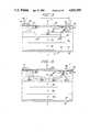
- FIG. 1is a cross-sectional illustration of a conventional insulated gate transistor
- FIG. 2is a cross-sectional illustration of the first embodiment of an insulated gate transistor constructed in accordance with the present invention
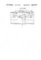
- FIG. 3is a cross-sectional illustration of an alternate embodiment of a MOS controlled thyristor constructed in accordance with the present invention
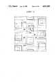
- FIG. 3Ais a top plan view of a preferred embodiment of a semiconductor device in accordance with the present invention taken along lines 3A--3A in FIG. 3;
- FIG. 4is an illustration of a top plan view of a cell layout wherein adjacent grids are interconnected by the devices themselves;
- FIG. 5is a cross-sectional illustration of a cell on an alternate device constructed in accordance with an alternate preferred embodiment of the present invention.
- FIGS. 6A-6Hare illustrations of an insulated gate transistor shown in successive steps of fabrication during the performance of a preferred method of fabricating the present invention.
- the present inventionprovides for the establishment of an insulated gate semiconductor device having improved resistance to inadvertent latched operation.
- the present inventionis applicable to a broad range of insulated gate semiconductor devices and can be fabricated from a variety of different semiconductor materials.
- the ensuing descriptionwill disclose several preferred embodiments of the improved insulated gate semiconductor device of the present invention as implemented in a silicon substrate because silicon devices or devices fabricated in silicon substrates make up an overwhelming majority of the currently available semiconductor devices. Consequently, the most commonly encountered applications of the present invention will involve silicon substrates. Nevertheless, it is intended that the invention disclosed herein can be advantageously employed in other semiconductor materials such as germanium or gallium arsenide and it is equally applicable to other semiconductor technologies. Accordingly, application of the present invention should not be limited to devices fabricated in silicon substrates, but instead should encompass those devices fabricated in any of a number of substrates.
- the present inventionis disclosed in a number of preferred embodiments directed to silicon substrates, it is intended that these disclosures be considered as illustrative examples of the preferred embodiment of the present invention and not as limitations on the scope of the applicability of the present invention.
- the illustrated examplesconcern the improved insulated gate semiconductor device in connection with an insulated gate transistor, it is recognized that the present invention is also applicable to other insulated gate semiconductor devices such as insulated gate thyristors in which it is desirable to avoid latching.
- the present inventionprovides for an increased latching threshold, it is also recognized that the attendant benefits of improved turn-off time can also be achieved.
- FIGS. 2 and 3Given the corresponding relationship of FIGS. 2 and 3, corresponding parts of these figures have been designated with the same reference numerals as an aid to understanding the description of the present invention. Various parts of the semiconductor elements, however, have not been drawn to scale. Certain dimensions have been exaggerated in relation to other dimensions in order to present a clearer understanding of the invention. Although for the purpose of illustration the preferred embodiment of the insulated gate semiconductor device of the present invention has been shown in each particular embodiment to include specific P and N type regions, it is understood by those skilled in the art that the teachings herein are equally applicable to insulated gate semiconductor devices in which the conductivities of the various regions have been reversed to, for instance, provide for the dual of the illustrated device.
- the device 10is illustrated to comprise a partially processed semiconductor wafer 12 shown as a first layer of one type conductivity material.
- one type conductivity materialhas been shown as P type material.
- the first layer 12has a first surface 14.
- a first electrode 16is disposed on the first surface 14 in ohmic contact with the first layer 12.
- the first layer 12can also comprise a heavily doped surface region such as a P+surface region adjacent the first surface 14 to facilitate the establishment of ohmic contact between the first electrode 16 and the first layer 12.
- the first layer 12also has a second surface 18 on which a second layer 20 illustrated as a moderately doped N type conductivity drift layer is disposed.
- the second layeralso has a surface 21.
- either the first layer 12 or the second layer 20can comprise the substrate with the other layer being established thereon by, for instance, epitaxial growth or doping techniques such as implantation or diffusion doping.
- a P+grid 22 shown as comprising a plurality of discrete P+regions 22a, 22b, 22c and 22dis established by, for instance, making spaced implantations of a heavy concentration of P or one type conductivity determining impurities to a prespecified depth beneath the surface 21 of the second layer.
- Each grid region 22a-22dis preferably implanted to a depth which is approximately equal to one and one-half times the maximum depth of the subsequently implanted first region or base region 24 (discussed below) to thus provide a grid 22 and hence a conductive path for one type conductivity carriers below and beneath the first or base region 24 of the device.
- the grid 22is illustrated to comprise only regions 22a, 22b, 22c and 22d, the grid can comprise any number of regions arranged in a substantially planar relationship beneath the first region 24 and equidistantly spaced beneath the first surface 21. It is preferred that the grid regions 22 be periodically interconnected by P or one type conductivity regions 23 shown in phantom in FIG. 2 to provide a P or one type conductivity path between the regions and to ensure the grid is a substantially equipotential plane.
- a first region 24 of P or one type conductivityis also disposed within the second layer of the device 10 and forms a PN junction 25 therewith.
- the first region 24 of the device 10preferably comprises a heavily doped central portion 26 extending to a depth which is greater than the depth of a more lightly doped perimeter portion 28 which partially surrounds the central region 26.
- the perimeter portion 28 of the first region 24forms a shallow shelf region while the central portion 26 forms a deep central portion of the first region 24. It is preferred that the deep portion of the first region 24 overlap and directly contact one or more of the regions 22a, 22b, 22c and 22d of the grid 22 to directly establish a one type conductivity conductive path betwee the grid 22 and the first region 24 and hence the cathode electrode 32.
- At least one portion such as regions 22a or 22d of the grid 22be separated from the first region 24 by a portion of the second layer 20 to define an opening 27 between adjacent grid regions 22a, 22b, 22d and 22d and also between the grid 22 and the first region 22 to foster the flow of opposite type carriers therebetween.
- One type conductivity carriersflow into the grid 22, into the first region 24 and to the cathode electrode 32.
- a second region 34 of opposite type conductivityis disposed within the first region 24 and forms a PN junction 35 therewith.
- the second region 34is preferably formed within the shelf portion 28 of the first region 24 and in combination with the second layer 20 defines channel portion 39 of the first region 24.
- a portion of the second region 34is disposed within the shallow shelf portion 28 of the first region and an additional portion of region 34 extends laterally above the deep portion 26 of the first region 24.
- a portion of the second region 34also overlies a portion of the grid 22 and more particularly, overlies region 22b of the grid 22 which is separated by the second layer 26 from the first region 24 and the main portion of the grid 22a.
- a first surface 21 of the device 10comprises a portion of the first surface 21 of the second layer 20, a portion of the surface of the second region 34 and a portion of the surface of the first region 24.
- An insulation layer 36such as silicon dioxide is disposed over the first surface 21 of the device and overlies a portion of the second region 34, the first region 24 and the second layer 20.
- a gate material 38such as doped polysilicon is disposed atop insulation layer 36 and overlies the second region 34, portion 28 of the first region 28 and a portion of the second layer 20.
- the second region 34 in combination with the second layer 20,defines the channel portion 39 of the first region 24 which is subject to insulated gate control.
- the insulated gate electrode 38in response to an appropriate applied bias, establishes an opposite type conductivity channel within the channel portion 39 of the first region 24 to facilitate the flow of opposite type conductivity carriers from the second region 34 through the channel portion 39 of the first region 24 and into the second layer 20. In response to removal of that bias, opposite type conductivity carriers cease to flow through the channel 39.
- a cathode electrode 32is preferably disposed on the first surface of the device 10 in ohmic contact with the first and second regions 24 and 34, respectively. It is preferred that the cathode electrode 32 short the PN junction 35 between the first and second regions 24 and 34, respectively where this junction 35 meets the surface 25 to inhibit the junction 35 from becoming forward biased.
- the grid 22is preferably disposed entirely beneath the shelf portion 28 of the first region 24 and also entirely beneath the channel 39.
- Each region of the gridpreferably has a lateral width L g equal to approximately 25% or less of the lateral width L b of the base region 24 of the device 10. Such construction ensures that an interstitial opening 27 will be disposed proximate the channel orifice into the second layer 20 proximate the intersection of the channel 39 with the second layer.
- Each grid region 22preferably comprises an oblong cylinder, a cross-section of which is shown in FIG. 2. In this cross-section, the radius of r 1 is greater than r 2 .
- the longitudinal or primary axis of the regionextends perpendicular to the plane of the illustrate.
- the orientation of the primary axis of the griddoes not matter.
- the primary axis of the grid 22is disposed transverse and substantially perpendicular to the longitudinal axis of the first and second regions 24 and 34, respectively.
- the longitudinal axis of the grid 22can be substantially parallel to the longitudinal axis of the first and second regions 24 and 34, respectively.
- opposite type conductivity carriersflow through the channel and recombine with P type conductivity carriers provided by the first layer.
- P type conductivity carriersalso flow from the first layer 12 through the second layer 20 and into the first region 24.
- the second region 34presents an obstruction to the direct flow of these carriers to the cathode electrode 32, these carriers flow closely adjacent the PN junction 35 the first and second regions 24 and 34, respectively.
- Ohm's lawpredicts the magnitude of the voltage drop which occurs along this junction 35.
- the PN junction 35becomes forward biased and P type conductivity carriers flow from the first region 24 into the second region 34 to forward bias the base emitter junction of an NPN transistor comprising the second layer 20, the first region 24 and the second region 34.
- a second PNP transistorcomprising the first layer 12, the second layer 20 and the first region 24 is also forward biased.
- a regenerative current flow between the first and second transistorsis established.
- the regenerative current flow between the first and second transistorlatches the device into a conductive mode without regard to the removal of the previously applied gate bias and hence a conductive path between the anode and cathode electrodes exits without regard to gate bias.
- the devicecan be turned off by removing or commutating the potential applied between the anode and cathode electrodes.
- the grid 22has been provided to establish a means for collecting one type carriers from the first layer 12 and providing a special current path for one type carriers.
- the one type conductivity carrier current pathis spaced and separated from the PN junction 35 to avoid establishing a voltage drop adjacent the junction 35.
- the illustrated embodimentshows a portion of grid 22 overlapping with the first region 24 and thus being directly connected through the first region 24 and to the cathode electrode 32, as previously explained, the grid 22 can also be coupled to a separate external collector electrode shown schematically by terminal 50 which may advantageously be connected to the cathode potential.
- P type conductivity carriersneed not flow in a vertical direction through the first region 24 to the cathode electrode 32, but can be separately channeled via, for instance, a separate collector electrode 50 illustrated schematically in FIG. 2.
- One type conductivity carrierscan be guided to the cathode electrode 32 away from the area of the first region 24 proximate the PN junction 35 not only by the illustrated configuration of the grid 22, but also by other configurations of the grid 22.
- a special potentialcan be applied to the external electrode 50 to make the alternate grid current paths more electrically attractive. It is thus within the scope of the present invention to provide a separate collector electrode 50 in contact with the grid 22 even when the grid 22 overlaps and directly connects to the first region 24.
- the collector electrode 50 attached to the grid 22can also be connected to the cathode electrode 32 of the device 10 or to the same potential as the cathode electrode to thus provide an alternate current path for the flow of P type conductivity carriers to the cathode potential of the device.
- the present inventioncan be employed in devices in which the size, configuration and doping concentration of the various regions can vary broadly over a wide range of values. It is thus difficult to specify any particular device parameters which would be said to encompass all preferred embodiment of the present invention. Nevertheless, by way of making a full disclosure of the present invention to the art, the below listed device regions can be fabricated with the specified parameters to provide a satisfactorily working device.
- FIG. 3Aan alternate preferred embodiment of the present invention is shown wherein the longitudinal axis of the grid 22 is disposed transverse and in a preferred embodiment, substantially perpendicular to the longitudinal axis of the first region 24.
- the gridprovides a low resistance current path which is transverse to the first region of the device 10 and thus facilitates the flow of hole current in this direction.
- FIG. 3Ais a top plan view of a portion of the structure of a cell as would be seen taken along lines 3A--3A of FIG. 3. More particularly, the longitudinal axis of the grid regions 22 extend transverse to the longitudinal axis of the first region 24 to facilitate the flow of carriers in a transverse direction. In a preferred embodiment, the longitudinal axis of grid 22 is disposed perpendicular to the longitudinal axis of the first region 24. While not shown in FIG. 3A, the grid 22 can be interconnected by cross connectors extending between adjacent grids.
- FIG. 4is an illustration of an alternate preferred embodiment of the present invention wherein a plurality of cells are shown to be arranged in a geometric pattern with respect to the grids 22.
- the first region 24interconnects the adjacent grid regions 22. More particularly, as illustrated, cell A interconnects grids 22a and 22b while cell B interconnects grids 22b and 22c and cell c interconnects grids 22c and 22d.
- the present inventioncan also be applied to provide other types of insulated gate semiconductor devices. More particularly, when the partially processed wafer 12 can comprise a first zone 40 of opposite type conductivity semiconductor material adjacent the first surface 14 of the and a second zone 42 of one type conductivity atop the the first zone with the first and second region being disposed in the second layer 20 to thus provide a MOS controlled thyristor. It is preferred that the grid 22 be entirely submerged beneath the second surface 21 of the device 10.
- the partially processed semiconductor wafer 12 used in fabricating the semiconductor device of the present inventionis shown to comprise a first layer 14 such as a layer of one type conductivity semiconductor material which is illustrated as P-type silicon material.
- a second layer 20 of opposite type conductivity semiconductor materialis disposed atop the first layer 12.
- either the first layer 14 of the second layer 20can be the substrate layer and the other layer can be disposed atop thereof by, for instance, epitaxial growth or doping techniques such as implantation or diffusion techniques.
- the second layer 20has a first surface 21.
- a first protective layer 40 such as silicon dioxideis provided atop the first surface 21 of the device 10. It is preferred that the partially processed wafer comprising the first and second layers 12 and 20, respectively is initially processed to establish the short grid regin 22 therein. More particularly, it is preferred that a series of implantations be performed with one type impurities, such as boron dopants, to provide a series of heavily doped one type conductivity regions disposed entirely beneath the surface 21 of the second layer 20 to establish a grid region 22 laterally disposed with the active region of the second layer 20. The implantations can be performed with impurities charged to greater than or equal to 300 KV for multiply charged ioned particles.
- one type impuritiessuch as boron dopants
- FIGS. 6A-1 and 6A-3An alternate method of establishing a body of semiconductor material containing a grid is shown in FIGS. 6A-1 and 6A-3.
- a body of semiconductor materialis provided having a first layer 12 of one type conductivity and first portion 20A of the second layer 20 of opposite type conductivity disposed thereon.
- the first portion 20A of the second layer 20is grown to within 2 to 5 microns of its final thickness.
- a first protective layer Pis provided on the exposed surface of the second layer 20A.
- a plurality of windows Ware opened through the first protective layer P as shown in FIG. 6A-2.
- the exposed surfaceis exposed to an impurity environment containing opposite type impurities and a plurality of opposite type conductivity regions are established within the second layer 20. Thereafter, as shown in FIG.
- a second portion 20B of the second layercan be established by epitaxial growth to thus cause the grid to lie entirely beneath the surface of the device. It should be noted that the grid region 22 can also be established by implantation followed by epitaxial growth of the second portion 20B of the second layer 20.
- a first window 42is opened through the first protective layer to expose a first portion 44 of the surface of the second layer 20 of the semiconductor device 10.
- the exposed surface portion 44 of the second layer 20is doped with a heavy concentration of one type conductivity dopants such as boron dopants by, for instance, implantation of diffusion techniques to establish a first portion 26 of the first region 24 comprising a heavy concentration of one type conductivity carriers.
- a second maskis used to open a second window 48 through the first protective layer 40 to expose a second surface portion 50 of the surface of the second layer 20.
- the second surface portion 50circumscribes and encompasses the first portion 44 of the second layer 20.
- a moderate concentration of one type conductivity impuritiessuch as boron impurities is introduced by, for instance, implantation or diffusion techniques into the second layer 20 and the first portion 26 of the first region 24 to establish a second portion 28 of the first region 24.
- the second portion 24extends to a depth which is less than the depth of the first portion 26 of the first region 24 and partially latterally surrounds the first portion 26 of the first region 24.
- the second portion 26is also less heavily doped that the first region 28.
- a second protective layer 54such as a silicon oxide layer 54 is formed within the second window 48.
- a third annular or ring-shaped window 64is opened through the second protective layer 54 to expose a third surface portion 66 of the surface 21 of the device 10.
- opposite type conductivity dopantssuch as arsenic dopants are introduced through the third window 64 into the first region 24 to establish a second region 34 of opposite type conductivity.
- a third protective layer 70such as a silicon dioxide layer is formed within the third window 64.
- a fourth window 74is opened through the second protective layer 54 and a portion of the third protective layer 70.
- a metallization layer 76such as aluminum is deposited within the fourth window 74 on the first surface to establish a cathode electrode 32 in ohmic contact with the first and second regions 24 and 34, respectively.
- the metal layer 76is applied over the insulation layer 70 to provide a gate electrode material 78 such as a metal.
- the gate materialcan be selected from the group comprising polysilicon, polysilicide and refractory metals. Tungsten is preferably deposited over the first insulation layer 40 and possibly a portion of the third insulation layer 70. The gate electrode material 78 thus overlies a second portion 28 of the first region 24 as well as a portion of the second region 34 and the second layer 20.
- first region 24be doped and driven in relation to the grid 22 so that in one embodiment, the first region 24 overlaps onto a portion of the grid 22 and in alternate embodiment, so that a region 22b of the grid 22 remains discrete and separated by the second layer 20 from the first region 24 to establish a separate grid region 22b of one type conductivity within the device.
- a separate electrode 30is provided to the heavily doped grid 22 by, for instance, providing a sinker region 80 of one type conductivity making contact with the grid 22, and providing a metallized contact within an extremity of the device to establish direct electrical connection to the heavily doped grid of the device. Electrical contact can also be established between the grid electrode 30 and the cathode electrode 22 to provide two cathode current paths for one type conductivity carriers.
- the extra short grid of the present inventionis equally applicable to other insulated gate semiconductor devices. Further, it is to be recognized that the inclusion of the extra short grid of the present invention within the insulated gate semiconductor device improves not only the latching threshold of the device, but also provides for improvements in other operating characteristics such as turn-off capability.
Landscapes
- Thyristors (AREA)
Abstract
Description
______________________________________ Doping Concentration Device Region (dopant atoms/cc) ______________________________________First layer 12 10.sup.18 -10.sup.21Second layer 20 10.sup.13 -10.sup.16Grid 22 10.sup.18 -10.sup.21First region 24 10.sup.16 -10.sup.20Second region 28 10.sup.16 -10.sup.18 ______________________________________
Claims (16)
Priority Applications (1)
| Application Number | Priority Date | Filing Date | Title |
|---|---|---|---|
| US07/025,036US4821095A (en) | 1987-03-12 | 1987-03-12 | Insulated gate semiconductor device with extra short grid and method of fabrication |
Applications Claiming Priority (1)
| Application Number | Priority Date | Filing Date | Title |
|---|---|---|---|
| US07/025,036US4821095A (en) | 1987-03-12 | 1987-03-12 | Insulated gate semiconductor device with extra short grid and method of fabrication |
Publications (1)
| Publication Number | Publication Date |
|---|---|
| US4821095Atrue US4821095A (en) | 1989-04-11 |
Family
ID=21823699
Family Applications (1)
| Application Number | Title | Priority Date | Filing Date |
|---|---|---|---|
| US07/025,036Expired - LifetimeUS4821095A (en) | 1987-03-12 | 1987-03-12 | Insulated gate semiconductor device with extra short grid and method of fabrication |
Country Status (1)
| Country | Link |
|---|---|
| US (1) | US4821095A (en) |
Cited By (62)
| Publication number | Priority date | Publication date | Assignee | Title |
|---|---|---|---|---|
| US4893165A (en)* | 1988-02-24 | 1990-01-09 | Siemens Aktiengesellschaft | Bipolar transistor controllable by field effect |
| US5043779A (en)* | 1989-07-21 | 1991-08-27 | Fuji Electric Co., Ltd. | Metal oxide semiconductor device with well region |
| US5122854A (en)* | 1989-06-29 | 1992-06-16 | Fuji Electric Co., Ltd. | MOS control thyristor |
| US5142348A (en)* | 1989-08-16 | 1992-08-25 | Matsushita Electronics Corporation | Lateral thyristor |
| US5173435A (en)* | 1987-11-11 | 1992-12-22 | Mitsubishi Denki Kabushiki Kaisha | Insulated gate bipolar transistor |
| US5212396A (en)* | 1983-11-30 | 1993-05-18 | Kabushiki Kaisha Toshiba | Conductivity modulated field effect transistor with optimized anode emitter and anode base impurity concentrations |
| EP0599221A1 (en)* | 1992-11-20 | 1994-06-01 | Hitachi, Ltd. | IGBT with bipolar transistor |
| US5331192A (en)* | 1989-06-15 | 1994-07-19 | Matsushita Electric Industrial Co., Ltd. | Semiconductor device |
| EP0616369A1 (en)* | 1993-02-16 | 1994-09-21 | Fuji Electric Co., Ltd. | MOS-type semiconductor device |
| US5468654A (en)* | 1987-08-19 | 1995-11-21 | Mitsubishi Denki Kabushiki Kaisha | Method of manufacturing an insulated gate bipolar transistor |
| US5519245A (en)* | 1989-08-31 | 1996-05-21 | Nippondenso Co., Ltd. | Insulated gate bipolar transistor with reverse conducting current |
| WO1998038681A1 (en)* | 1997-02-25 | 1998-09-03 | Siemens Aktiengesellschaft | Field effect controllable semiconductor component |
| WO1999039388A1 (en)* | 1998-01-29 | 1999-08-05 | Siemens Aktiengesellschaft | Semiconductor insulating structure with reduced surface field strength and method for the production of the said structure |
| WO2000002250A1 (en)* | 1998-07-07 | 2000-01-13 | Infineon Technologies Ag | Vertical semiconductor element with reduced electric surface field |
| US6034415A (en)* | 1998-02-07 | 2000-03-07 | Xemod, Inc. | Lateral RF MOS device having a combined source structure |
| US6091108A (en)* | 1997-11-13 | 2000-07-18 | Abb Research Ltd. | Semiconductor device of SiC having an insulated gate and buried grid region for high breakdown voltage |
| US20030173624A1 (en)* | 2002-02-23 | 2003-09-18 | Fairchild Korea Semiconductor Ltd. | High breakdown voltage low on-resistance lateral DMOS transistor |
| US6635906B1 (en)* | 1993-10-29 | 2003-10-21 | Third Dimension (3D) Semiconductor | Voltage sustaining layer with opposite-doped islands for semi-conductor power devices |
| US6667500B2 (en)* | 2000-02-23 | 2003-12-23 | Motorola, Inc. | Semiconductor device and method for protecting such device from a reversed drain voltage |
| US20040021173A1 (en)* | 2002-07-30 | 2004-02-05 | Fairchild Semiconductor Corporation | Dual trench power mosfet |
| US6710418B1 (en) | 2002-10-11 | 2004-03-23 | Fairchild Semiconductor Corporation | Schottky rectifier with insulation-filled trenches and method of forming the same |
| US20040065919A1 (en)* | 2002-10-03 | 2004-04-08 | Wilson Peter H. | Trench gate laterally diffused MOSFET devices and methods for making such devices |
| US20040115790A1 (en)* | 2001-02-13 | 2004-06-17 | Tiina Pakula | Method for production of secreted proteins in fungi |
| US20040142523A1 (en)* | 2000-08-16 | 2004-07-22 | Izak Bencuya | Method of forming vertical mosfet with ultra-low on-resistance and low gate charge |
| US6803626B2 (en) | 2002-07-18 | 2004-10-12 | Fairchild Semiconductor Corporation | Vertical charge control semiconductor device |
| US20040232407A1 (en)* | 1999-12-20 | 2004-11-25 | Fairchild Semiconductor Corporation | Power MOS device with improved gate charge performance |
| US20040232481A1 (en)* | 2003-05-20 | 2004-11-25 | Robert Herrick | Structure and method for forming a trench MOSFET having self-aligned features |
| US20040256690A1 (en)* | 2001-10-17 | 2004-12-23 | Kocon Christopher Boguslaw | Schottky diode using charge balance structure |
| US20050029618A1 (en)* | 2001-01-30 | 2005-02-10 | Marchant Bruce D. | Structure and method of forming a dual-trench field effect transistor |
| US20050116313A1 (en)* | 2003-11-28 | 2005-06-02 | Lee Jae-Gil | Superjunction semiconductor device |
| US20050153497A1 (en)* | 2000-08-16 | 2005-07-14 | Izak Bencuya | Method of forming a FET having ultra-low on-resistance and low gate charge |
| US20050167742A1 (en)* | 2001-01-30 | 2005-08-04 | Fairchild Semiconductor Corp. | Power semiconductor devices and methods of manufacture |
| US20050199918A1 (en)* | 2004-03-15 | 2005-09-15 | Daniel Calafut | Optimized trench power MOSFET with integrated schottky diode |
| US20060011962A1 (en)* | 2003-12-30 | 2006-01-19 | Kocon Christopher B | Accumulation device with charge balance structure and method of forming the same |
| US6991977B2 (en) | 2001-10-17 | 2006-01-31 | Fairchild Semiconductor Corporation | Method for forming a semiconductor structure with improved smaller forward voltage loss and higher blocking capability |
| US20060030142A1 (en)* | 2004-08-03 | 2006-02-09 | Grebs Thomas E | Semiconductor power device having a top-side drain using a sinker trench |
| US20060076617A1 (en)* | 2004-10-08 | 2006-04-13 | Shenoy Praveen M | MOS-gated transistor with reduced miller capacitance |
| US20060145191A1 (en)* | 2003-02-18 | 2006-07-06 | Koninklijke Philips Electronics N.V. | Semiconductor device and method of manufacturing such a device |
| US20060214221A1 (en)* | 2003-05-20 | 2006-09-28 | Ashok Challa | Power semiconductor devices and methods of manufacture |
| US7132712B2 (en) | 2002-11-05 | 2006-11-07 | Fairchild Semiconductor Corporation | Trench structure having one or more diodes embedded therein adjacent a PN junction |
| US20060267090A1 (en)* | 2005-04-06 | 2006-11-30 | Steven Sapp | Trenched-gate field effect transistors and methods of forming the same |
| US7319256B1 (en) | 2006-06-19 | 2008-01-15 | Fairchild Semiconductor Corporation | Shielded gate trench FET with the shield and gate electrodes being connected together |
| US20080036015A1 (en)* | 2006-08-14 | 2008-02-14 | Icemos Technology Corporation | Semiconductor devices with sealed, unlined trenches and methods of forming same |
| US20080090339A1 (en)* | 2005-08-09 | 2008-04-17 | Robert Herrick | Method for Forming Inter-Poly Dielectric in Shielded Gate Field Effect Transistor |
| US20080258239A1 (en)* | 2007-04-23 | 2008-10-23 | Icemos Technology Corporation | Methods for manufacturing a trench type semiconductor device having a thermally sensitive refill material |
| US20080258226A1 (en)* | 2007-04-23 | 2008-10-23 | Icemos Technology Corporation | Methods for manufacturing a trench type semiconductor device having a thermally sensitive refill material |
| US7446374B2 (en) | 2006-03-24 | 2008-11-04 | Fairchild Semiconductor Corporation | High density trench FET with integrated Schottky diode and method of manufacture |
| US20080272429A1 (en)* | 2007-05-04 | 2008-11-06 | Icemos Technology Corporation | Superjunction devices having narrow surface layout of terminal structures and methods of manufacturing the devices |
| US20090079002A1 (en)* | 2007-09-21 | 2009-03-26 | Jaegil Lee | Superjunction Structures for Power Devices and Methods of Manufacture |
| US20090085148A1 (en)* | 2007-09-28 | 2009-04-02 | Icemos Technology Corporation | Multi-directional trenching of a plurality of dies in manufacturing superjunction devices |
| US20090166672A1 (en)* | 2007-12-31 | 2009-07-02 | Alpha & Omega Semiconductor, Ltd. | Sawtooth electric field drift region structure for power semiconductor devices |
| US20090166728A1 (en)* | 2007-12-26 | 2009-07-02 | James Pan | Structure and Method for Forming Shielded Gate Trench FET with Multiple Channels |
| US20090200634A1 (en)* | 2008-02-13 | 2009-08-13 | Icemos Technology Ltd. | Multi-angle rotation for ion implantation of trenches in superjunction devices |
| US7576388B1 (en) | 2002-10-03 | 2009-08-18 | Fairchild Semiconductor Corporation | Trench-gate LDMOS structures |
| US8319290B2 (en) | 2010-06-18 | 2012-11-27 | Fairchild Semiconductor Corporation | Trench MOS barrier schottky rectifier with a planar surface using CMP techniques |
| US8673700B2 (en) | 2011-04-27 | 2014-03-18 | Fairchild Semiconductor Corporation | Superjunction structures for power devices and methods of manufacture |
| US8772868B2 (en) | 2011-04-27 | 2014-07-08 | Fairchild Semiconductor Corporation | Superjunction structures for power devices and methods of manufacture |
| US8786010B2 (en) | 2011-04-27 | 2014-07-22 | Fairchild Semiconductor Corporation | Superjunction structures for power devices and methods of manufacture |
| US8836028B2 (en) | 2011-04-27 | 2014-09-16 | Fairchild Semiconductor Corporation | Superjunction structures for power devices and methods of manufacture |
| US8946814B2 (en) | 2012-04-05 | 2015-02-03 | Icemos Technology Ltd. | Superjunction devices having narrow surface layout of terminal structures, buried contact regions and trench gates |
| US8963212B2 (en) | 2008-12-08 | 2015-02-24 | Fairchild Semiconductor Corporation | Trench-based power semiconductor devices with increased breakdown voltage characteristics |
| US9431481B2 (en) | 2008-09-19 | 2016-08-30 | Fairchild Semiconductor Corporation | Superjunction structures for power devices and methods of manufacture |
Citations (9)
| Publication number | Priority date | Publication date | Assignee | Title |
|---|---|---|---|---|
| US3465216A (en)* | 1966-07-22 | 1969-09-02 | Stanislas Teszner | Bistable semiconductor device for heavy currents |
| US3831187A (en)* | 1973-04-11 | 1974-08-20 | Rca Corp | Thyristor having capacitively coupled control electrode |
| US4275408A (en)* | 1979-07-09 | 1981-06-23 | Mitsubishi Denki Kabushiki Kaisha | Thyristor |
| US4466175A (en)* | 1981-06-17 | 1984-08-21 | U.S. Philips Corporation | Manufacture of vertical insulated gate field effect transistors |
| US4466176A (en)* | 1982-08-09 | 1984-08-21 | General Electric Company | Process for manufacturing insulated-gate semiconductor devices with integral shorts |
| US4503598A (en)* | 1982-05-20 | 1985-03-12 | Fairchild Camera & Instrument Corporation | Method of fabricating power MOSFET structure utilizing self-aligned diffusion and etching techniques |
| US4587713A (en)* | 1984-02-22 | 1986-05-13 | Rca Corporation | Method for making vertical MOSFET with reduced bipolar effects |
| US4680604A (en)* | 1984-03-19 | 1987-07-14 | Kabushiki Kaisha Toshiba | Conductivity modulated MOS transistor device |
| US4717940A (en)* | 1986-03-11 | 1988-01-05 | Kabushiki Kaisha Toshiba | MIS controlled gate turn-off thyristor |
- 1987
- 1987-03-12USUS07/025,036patent/US4821095A/ennot_activeExpired - Lifetime
Patent Citations (9)
| Publication number | Priority date | Publication date | Assignee | Title |
|---|---|---|---|---|
| US3465216A (en)* | 1966-07-22 | 1969-09-02 | Stanislas Teszner | Bistable semiconductor device for heavy currents |
| US3831187A (en)* | 1973-04-11 | 1974-08-20 | Rca Corp | Thyristor having capacitively coupled control electrode |
| US4275408A (en)* | 1979-07-09 | 1981-06-23 | Mitsubishi Denki Kabushiki Kaisha | Thyristor |
| US4466175A (en)* | 1981-06-17 | 1984-08-21 | U.S. Philips Corporation | Manufacture of vertical insulated gate field effect transistors |
| US4503598A (en)* | 1982-05-20 | 1985-03-12 | Fairchild Camera & Instrument Corporation | Method of fabricating power MOSFET structure utilizing self-aligned diffusion and etching techniques |
| US4466176A (en)* | 1982-08-09 | 1984-08-21 | General Electric Company | Process for manufacturing insulated-gate semiconductor devices with integral shorts |
| US4587713A (en)* | 1984-02-22 | 1986-05-13 | Rca Corporation | Method for making vertical MOSFET with reduced bipolar effects |
| US4680604A (en)* | 1984-03-19 | 1987-07-14 | Kabushiki Kaisha Toshiba | Conductivity modulated MOS transistor device |
| US4717940A (en)* | 1986-03-11 | 1988-01-05 | Kabushiki Kaisha Toshiba | MIS controlled gate turn-off thyristor |
Cited By (178)
| Publication number | Priority date | Publication date | Assignee | Title |
|---|---|---|---|---|
| US5212396A (en)* | 1983-11-30 | 1993-05-18 | Kabushiki Kaisha Toshiba | Conductivity modulated field effect transistor with optimized anode emitter and anode base impurity concentrations |
| US5468654A (en)* | 1987-08-19 | 1995-11-21 | Mitsubishi Denki Kabushiki Kaisha | Method of manufacturing an insulated gate bipolar transistor |
| US5173435A (en)* | 1987-11-11 | 1992-12-22 | Mitsubishi Denki Kabushiki Kaisha | Insulated gate bipolar transistor |
| US4893165A (en)* | 1988-02-24 | 1990-01-09 | Siemens Aktiengesellschaft | Bipolar transistor controllable by field effect |
| US5331192A (en)* | 1989-06-15 | 1994-07-19 | Matsushita Electric Industrial Co., Ltd. | Semiconductor device |
| US5122854A (en)* | 1989-06-29 | 1992-06-16 | Fuji Electric Co., Ltd. | MOS control thyristor |
| US5043779A (en)* | 1989-07-21 | 1991-08-27 | Fuji Electric Co., Ltd. | Metal oxide semiconductor device with well region |
| US5142348A (en)* | 1989-08-16 | 1992-08-25 | Matsushita Electronics Corporation | Lateral thyristor |
| US5519245A (en)* | 1989-08-31 | 1996-05-21 | Nippondenso Co., Ltd. | Insulated gate bipolar transistor with reverse conducting current |
| US5572048A (en)* | 1992-11-20 | 1996-11-05 | Hitachi, Ltd. | Voltage-driven type semiconductor device |
| EP0599221A1 (en)* | 1992-11-20 | 1994-06-01 | Hitachi, Ltd. | IGBT with bipolar transistor |
| EP0616369A1 (en)* | 1993-02-16 | 1994-09-21 | Fuji Electric Co., Ltd. | MOS-type semiconductor device |
| US5397905A (en)* | 1993-02-16 | 1995-03-14 | Fuji Electric Co., Ltd. | Power semiconductor device having an insulated gate field effect transistor and a bipolar transistor |
| US20070272999A1 (en)* | 1993-04-27 | 2007-11-29 | Third Dimension (3D) Semiconductor, Inc. | Voltage Sustaining Layer with Opposite-Doped Islands for Semiconductor Power Devices |
| US20090130828A1 (en)* | 1993-10-29 | 2009-05-21 | Third Dimension (3D) Semiconductor, Inc. | Method for Forming Voltage Sustaining Layer with Opposite-Doped Islands for Semiconductor Power Devices |
| US7227197B2 (en) | 1993-10-29 | 2007-06-05 | Third Dimension (3D) Semiconductor, Inc. | Semiconductor high-voltage devices |
| US7271067B2 (en) | 1993-10-29 | 2007-09-18 | Third Dimension (3D) Semiconductor, Inc. | Voltage sustaining layer with opposite-doped islands for semiconductor power devices |
| US20060177995A1 (en)* | 1993-10-29 | 2006-08-10 | Third Dimension (3D) Semiconductor, Inc. | Voltage sustaining layer with opposite-doped islands for semiconductor power devices |
| US8071450B2 (en) | 1993-10-29 | 2011-12-06 | Third Dimension (3D) Semiconductor, Inc. | Method for forming voltage sustaining layer with opposite-doped islands for semiconductor power devices |
| US20050035406A1 (en)* | 1993-10-29 | 2005-02-17 | Xingbi Chen | Semiconductor high-voltage devices |
| US7498614B2 (en) | 1993-10-29 | 2009-03-03 | Third Dimension (3D) Semiconductor, Inc. | Voltage sustaining layer with opposite-doped islands for semiconductor power devices |
| US6635906B1 (en)* | 1993-10-29 | 2003-10-21 | Third Dimension (3D) Semiconductor | Voltage sustaining layer with opposite-doped islands for semi-conductor power devices |
| US6147381A (en)* | 1997-02-25 | 2000-11-14 | Infineon Technologies Ag | Field effect-controllable semiconductor component |
| WO1998038681A1 (en)* | 1997-02-25 | 1998-09-03 | Siemens Aktiengesellschaft | Field effect controllable semiconductor component |
| US6091108A (en)* | 1997-11-13 | 2000-07-18 | Abb Research Ltd. | Semiconductor device of SiC having an insulated gate and buried grid region for high breakdown voltage |
| WO1999039388A1 (en)* | 1998-01-29 | 1999-08-05 | Siemens Aktiengesellschaft | Semiconductor insulating structure with reduced surface field strength and method for the production of the said structure |
| US6034415A (en)* | 1998-02-07 | 2000-03-07 | Xemod, Inc. | Lateral RF MOS device having a combined source structure |
| WO2000002250A1 (en)* | 1998-07-07 | 2000-01-13 | Infineon Technologies Ag | Vertical semiconductor element with reduced electric surface field |
| US6847091B2 (en) | 1998-07-07 | 2005-01-25 | Infineon Technologies Ag | Vertical semiconductor component having a reduced electrical surface field |
| US7625793B2 (en) | 1999-12-20 | 2009-12-01 | Fairchild Semiconductor Corporation | Power MOS device with improved gate charge performance |
| US20040232407A1 (en)* | 1999-12-20 | 2004-11-25 | Fairchild Semiconductor Corporation | Power MOS device with improved gate charge performance |
| US20060024890A1 (en)* | 1999-12-20 | 2006-02-02 | Calafut Daniel S | Power MOS device with improved gate charge performance |
| US6667500B2 (en)* | 2000-02-23 | 2003-12-23 | Motorola, Inc. | Semiconductor device and method for protecting such device from a reversed drain voltage |
| US8710584B2 (en) | 2000-08-16 | 2014-04-29 | Fairchild Semiconductor Corporation | FET device having ultra-low on-resistance and low gate charge |
| US20040142523A1 (en)* | 2000-08-16 | 2004-07-22 | Izak Bencuya | Method of forming vertical mosfet with ultra-low on-resistance and low gate charge |
| US7745289B2 (en) | 2000-08-16 | 2010-06-29 | Fairchild Semiconductor Corporation | Method of forming a FET having ultra-low on-resistance and low gate charge |
| US20050153497A1 (en)* | 2000-08-16 | 2005-07-14 | Izak Bencuya | Method of forming a FET having ultra-low on-resistance and low gate charge |
| US8101484B2 (en) | 2000-08-16 | 2012-01-24 | Fairchild Semiconductor Corporation | Method of forming a FET having ultra-low on-resistance and low gate charge |
| US20100258864A1 (en)* | 2000-08-16 | 2010-10-14 | Izak Bencuya | Method of Forming a FET Having Ultra-low On-resistance and Low Gate Charge |
| US7345342B2 (en) | 2001-01-30 | 2008-03-18 | Fairchild Semiconductor Corporation | Power semiconductor devices and methods of manufacture |
| US8829641B2 (en) | 2001-01-30 | 2014-09-09 | Fairchild Semiconductor Corporation | Method of forming a dual-trench field effect transistor |
| US20050167742A1 (en)* | 2001-01-30 | 2005-08-04 | Fairchild Semiconductor Corp. | Power semiconductor devices and methods of manufacture |
| US20050029618A1 (en)* | 2001-01-30 | 2005-02-10 | Marchant Bruce D. | Structure and method of forming a dual-trench field effect transistor |
| US9368587B2 (en) | 2001-01-30 | 2016-06-14 | Fairchild Semiconductor Corporation | Accumulation-mode field effect transistor with improved current capability |
| US20110014764A1 (en)* | 2001-01-30 | 2011-01-20 | Marchant Bruce D | Method of forming a dual-trench field effect transistor |
| US20040115790A1 (en)* | 2001-02-13 | 2004-06-17 | Tiina Pakula | Method for production of secreted proteins in fungi |
| US20040256690A1 (en)* | 2001-10-17 | 2004-12-23 | Kocon Christopher Boguslaw | Schottky diode using charge balance structure |
| US20060166473A1 (en)* | 2001-10-17 | 2006-07-27 | Kocon Christopher B | Method of forming schottky diode with charge balance structure |
| US7061066B2 (en) | 2001-10-17 | 2006-06-13 | Fairchild Semiconductor Corporation | Schottky diode using charge balance structure |
| US7429523B2 (en) | 2001-10-17 | 2008-09-30 | Fairchild Semiconductor Corporation | Method of forming schottky diode with charge balance structure |
| US6991977B2 (en) | 2001-10-17 | 2006-01-31 | Fairchild Semiconductor Corporation | Method for forming a semiconductor structure with improved smaller forward voltage loss and higher blocking capability |
| US7265416B2 (en) | 2002-02-23 | 2007-09-04 | Fairchild Korea Semiconductor Ltd. | High breakdown voltage low on-resistance lateral DMOS transistor |
| US20030173624A1 (en)* | 2002-02-23 | 2003-09-18 | Fairchild Korea Semiconductor Ltd. | High breakdown voltage low on-resistance lateral DMOS transistor |
| US7605040B2 (en) | 2002-02-23 | 2009-10-20 | Fairchild Korea Semiconductor Ltd. | Method of forming high breakdown voltage low on-resistance lateral DMOS transistor |
| US20070264785A1 (en)* | 2002-02-23 | 2007-11-15 | Yong-Cheol Choi | Method of Forming High Breakdown Voltage Low On-Resistance Lateral DMOS Transistor |
| US7291894B2 (en) | 2002-07-18 | 2007-11-06 | Fairchild Semiconductor Corporation | Vertical charge control semiconductor device with low output capacitance |
| US20050023607A1 (en)* | 2002-07-18 | 2005-02-03 | Steven Sapp | Vertical charge control semiconductor device with low output capacitance |
| US6803626B2 (en) | 2002-07-18 | 2004-10-12 | Fairchild Semiconductor Corporation | Vertical charge control semiconductor device |
| US7977744B2 (en) | 2002-07-18 | 2011-07-12 | Fairchild Semiconductor Corporation | Field effect transistor with trench filled with insulating material and strips of semi-insulating material along trench sidewalls |
| US6710403B2 (en) | 2002-07-30 | 2004-03-23 | Fairchild Semiconductor Corporation | Dual trench power MOSFET |
| US20040021173A1 (en)* | 2002-07-30 | 2004-02-05 | Fairchild Semiconductor Corporation | Dual trench power mosfet |
| US20090273026A1 (en)* | 2002-10-03 | 2009-11-05 | Wilson Peter H | Trench-gate ldmos structures |
| US8198677B2 (en) | 2002-10-03 | 2012-06-12 | Fairchild Semiconductor Corporation | Trench-gate LDMOS structures |
| US7033891B2 (en) | 2002-10-03 | 2006-04-25 | Fairchild Semiconductor Corporation | Trench gate laterally diffused MOSFET devices and methods for making such devices |
| US20040065919A1 (en)* | 2002-10-03 | 2004-04-08 | Wilson Peter H. | Trench gate laterally diffused MOSFET devices and methods for making such devices |
| US7576388B1 (en) | 2002-10-03 | 2009-08-18 | Fairchild Semiconductor Corporation | Trench-gate LDMOS structures |
| US6710418B1 (en) | 2002-10-11 | 2004-03-23 | Fairchild Semiconductor Corporation | Schottky rectifier with insulation-filled trenches and method of forming the same |
| US7582519B2 (en) | 2002-11-05 | 2009-09-01 | Fairchild Semiconductor Corporation | Method of forming a trench structure having one or more diodes embedded therein adjacent a PN junction |
| US7132712B2 (en) | 2002-11-05 | 2006-11-07 | Fairchild Semiconductor Corporation | Trench structure having one or more diodes embedded therein adjacent a PN junction |
| US7728404B2 (en)* | 2003-02-18 | 2010-06-01 | Nxp B.V. | Punchthrough diode and method of manufacturing thereof |
| US20060145191A1 (en)* | 2003-02-18 | 2006-07-06 | Koninklijke Philips Electronics N.V. | Semiconductor device and method of manufacturing such a device |
| US20090026500A1 (en)* | 2003-02-18 | 2009-01-29 | Rob Van Dalen | Semiconductor Device and Method of Manufacturing Such a Device |
| US7482669B2 (en)* | 2003-02-18 | 2009-01-27 | Nxp B.V. | Semiconductor device and method of manufacturing such a device |
| US7982265B2 (en) | 2003-05-20 | 2011-07-19 | Fairchild Semiconductor Corporation | Trenched shield gate power semiconductor devices and methods of manufacture |
| US8350317B2 (en) | 2003-05-20 | 2013-01-08 | Fairchild Semiconductor Corporation | Power semiconductor devices and methods of manufacture |
| US20080150020A1 (en)* | 2003-05-20 | 2008-06-26 | Ashok Challa | Trenched Shield Gate Power Semiconductor Devices and Methods of Manufacture |
| US20080164519A1 (en)* | 2003-05-20 | 2008-07-10 | Robert Herrick | Power Device with Trenches Having Wider Upper Portion than Lower Portion |
| US20080199997A1 (en)* | 2003-05-20 | 2008-08-21 | Grebs Thomas E | Methods of Forming Inter-poly Dielectric (IPD) Layers in Power Semiconductor Devices |
| US20080197407A1 (en)* | 2003-05-20 | 2008-08-21 | Ashok Challa | Power Semiconductor Devices with Barrier Layer to Reduce Substrate Up-Diffusion and Methods of Manufacture |
| US20040232481A1 (en)* | 2003-05-20 | 2004-11-25 | Robert Herrick | Structure and method for forming a trench MOSFET having self-aligned features |
| US7638841B2 (en) | 2003-05-20 | 2009-12-29 | Fairchild Semiconductor Corporation | Power semiconductor devices and methods of manufacture |
| US20080138953A1 (en)* | 2003-05-20 | 2008-06-12 | Ashok Challa | Methods of Making Power Semiconductor Devices with Thick Bottom Oxide Layer |
| US8936985B2 (en) | 2003-05-20 | 2015-01-20 | Fairchild Semiconductor Corporation | Methods related to power semiconductor devices with thick bottom oxide layers |
| US8889511B2 (en) | 2003-05-20 | 2014-11-18 | Fairchild Semiconductor Corporation | Methods of manufacturing power semiconductor devices with trenched shielded split gate transistor |
| US20100015769A1 (en)* | 2003-05-20 | 2010-01-21 | Robert Herrick | Power Device With Trenches Having Wider Upper Portion Than Lower Portion |
| US8786045B2 (en) | 2003-05-20 | 2014-07-22 | Fairchild Semiconductor Corporation | Power semiconductor devices having termination structures |
| US8716783B2 (en) | 2003-05-20 | 2014-05-06 | Fairchild Semiconductor Corporation | Power device with self-aligned source regions |
| US20090008709A1 (en)* | 2003-05-20 | 2009-01-08 | Yedinak Joseph A | Power Semiconductor Devices with Trenched Shielded Split Gate Transistor and Methods of Manufacture |
| US20080135931A1 (en)* | 2003-05-20 | 2008-06-12 | Ashok Challa | Power Semiconductor Devices Having Termination Structures and Methods of Manufacture |
| US6916745B2 (en) | 2003-05-20 | 2005-07-12 | Fairchild Semiconductor Corporation | Structure and method for forming a trench MOSFET having self-aligned features |
| US7595524B2 (en) | 2003-05-20 | 2009-09-29 | Fairchild Semiconductor Corporation | Power device with trenches having wider upper portion than lower portion |
| US8143124B2 (en) | 2003-05-20 | 2012-03-27 | Fairchild Semiconductor Corporation | Methods of making power semiconductor devices with thick bottom oxide layer |
| US8143123B2 (en) | 2003-05-20 | 2012-03-27 | Fairchild Semiconductor Corporation | Methods of forming inter-poly dielectric (IPD) layers in power semiconductor devices |
| US8129245B2 (en) | 2003-05-20 | 2012-03-06 | Fairchild Semiconductor Corporation | Methods of manufacturing power semiconductor devices with shield and gate contacts |
| US8034682B2 (en) | 2003-05-20 | 2011-10-11 | Fairchild Semiconductor Corporation | Power device with trenches having wider upper portion than lower portion |
| US8013391B2 (en) | 2003-05-20 | 2011-09-06 | Fairchild Semiconductor Corporation | Power semiconductor devices with trenched shielded split gate transistor and methods of manufacture |
| US8013387B2 (en) | 2003-05-20 | 2011-09-06 | Fairchild Semiconductor Corporation | Power semiconductor devices with shield and gate contacts and methods of manufacture |
| US20060214221A1 (en)* | 2003-05-20 | 2006-09-28 | Ashok Challa | Power semiconductor devices and methods of manufacture |
| US20060214222A1 (en)* | 2003-05-20 | 2006-09-28 | Ashok Challa | Power semiconductor devices and methods of manufacture |
| US20110003449A1 (en)* | 2003-05-20 | 2011-01-06 | Robert Herrick | Power Device With Trenches Having Wider Upper Portion Than Lower Portion |
| US20110001189A1 (en)* | 2003-05-20 | 2011-01-06 | Ashok Challa | Power Semiconductor Devices Having Termination Structures |
| US7855415B2 (en) | 2003-05-20 | 2010-12-21 | Fairchild Semiconductor Corporation | Power semiconductor devices having termination structures and methods of manufacture |
| US7799636B2 (en) | 2003-05-20 | 2010-09-21 | Fairchild Semiconductor Corporation | Power device with trenches having wider upper portion than lower portion |
| US7652326B2 (en) | 2003-05-20 | 2010-01-26 | Fairchild Semiconductor Corporation | Power semiconductor devices and methods of manufacture |
| US7344943B2 (en) | 2003-05-20 | 2008-03-18 | Fairchild Semiconductor Corporation | Method for forming a trench MOSFET having self-aligned features |
| US7655981B2 (en) | 2003-11-28 | 2010-02-02 | Fairchild Korea Semiconductor Ltd. | Superjunction semiconductor device |
| US7301203B2 (en) | 2003-11-28 | 2007-11-27 | Fairchild Korea Semiconductor Ltd. | Superjunction semiconductor device |
| US20050116313A1 (en)* | 2003-11-28 | 2005-06-02 | Lee Jae-Gil | Superjunction semiconductor device |
| US20080211053A1 (en)* | 2003-11-28 | 2008-09-04 | Fairchild Korea Semiconductor Ltd. | Superjunction Semiconductor Device |
| US8518777B2 (en) | 2003-12-30 | 2013-08-27 | Fairchild Semiconductor Corporation | Method for forming accumulation-mode field effect transistor with improved current capability |
| US20080211012A1 (en)* | 2003-12-30 | 2008-09-04 | Christopher Boguslaw Kocon | Structure and Method for Forming Accumulation-mode Field Effect Transistor with Improved Current Capability |
| US20060011962A1 (en)* | 2003-12-30 | 2006-01-19 | Kocon Christopher B | Accumulation device with charge balance structure and method of forming the same |
| US7368777B2 (en) | 2003-12-30 | 2008-05-06 | Fairchild Semiconductor Corporation | Accumulation device with charge balance structure and method of forming the same |
| US7936008B2 (en) | 2003-12-30 | 2011-05-03 | Fairchild Semiconductor Corporation | Structure and method for forming accumulation-mode field effect transistor with improved current capability |
| US20050199918A1 (en)* | 2004-03-15 | 2005-09-15 | Daniel Calafut | Optimized trench power MOSFET with integrated schottky diode |
| US20080142883A1 (en)* | 2004-08-03 | 2008-06-19 | Grebs Thomas E | Power Transistor with Trench Sinker for Contacting the Backside |
| US8026558B2 (en) | 2004-08-03 | 2011-09-27 | Fairchild Semiconductor Corporation | Semiconductor power device having a top-side drain using a sinker trench |
| US7352036B2 (en) | 2004-08-03 | 2008-04-01 | Fairchild Semiconductor Corporation | Semiconductor power device having a top-side drain using a sinker trench |
| US20060030142A1 (en)* | 2004-08-03 | 2006-02-09 | Grebs Thomas E | Semiconductor power device having a top-side drain using a sinker trench |
| US7732876B2 (en) | 2004-08-03 | 2010-06-08 | Fairchild Semiconductor Corporation | Power transistor with trench sinker for contacting the backside |
| US8148233B2 (en) | 2004-08-03 | 2012-04-03 | Fairchild Semiconductor Corporation | Semiconductor power device having a top-side drain using a sinker trench |
| US20070264782A1 (en)* | 2004-10-08 | 2007-11-15 | Shenoy Praveen M | Method of Making a MOS-Gated Transistor with Reduced Miller Capacitance |
| US7534683B2 (en) | 2004-10-08 | 2009-05-19 | Fairchild Semiconductor Corporation | Method of making a MOS-gated transistor with reduced miller capacitance |
| US20060076617A1 (en)* | 2004-10-08 | 2006-04-13 | Shenoy Praveen M | MOS-gated transistor with reduced miller capacitance |
| US7265415B2 (en) | 2004-10-08 | 2007-09-04 | Fairchild Semiconductor Corporation | MOS-gated transistor with reduced miller capacitance |
| US8084327B2 (en) | 2005-04-06 | 2011-12-27 | Fairchild Semiconductor Corporation | Method for forming trench gate field effect transistor with recessed mesas using spacers |
| US7504306B2 (en) | 2005-04-06 | 2009-03-17 | Fairchild Semiconductor Corporation | Method of forming trench gate field effect transistor with recessed mesas |
| US20060267090A1 (en)* | 2005-04-06 | 2006-11-30 | Steven Sapp | Trenched-gate field effect transistors and methods of forming the same |
| US20090111227A1 (en)* | 2005-04-06 | 2009-04-30 | Christopher Boguslaw Kocon | Method for Forming Trench Gate Field Effect Transistor with Recessed Mesas Using Spacers |
| US8680611B2 (en) | 2005-04-06 | 2014-03-25 | Fairchild Semiconductor Corporation | Field effect transistor and schottky diode structures |
| US7385248B2 (en) | 2005-08-09 | 2008-06-10 | Fairchild Semiconductor Corporation | Shielded gate field effect transistor with improved inter-poly dielectric |
| US20080090339A1 (en)* | 2005-08-09 | 2008-04-17 | Robert Herrick | Method for Forming Inter-Poly Dielectric in Shielded Gate Field Effect Transistor |
| US7598144B2 (en) | 2005-08-09 | 2009-10-06 | Fairchild Semiconductor Corporation | Method for forming inter-poly dielectric in shielded gate field effect transistor |
| US20090035900A1 (en)* | 2006-03-24 | 2009-02-05 | Paul Thorup | Method of Forming High Density Trench FET with Integrated Schottky Diode |
| US7713822B2 (en) | 2006-03-24 | 2010-05-11 | Fairchild Semiconductor Corporation | Method of forming high density trench FET with integrated Schottky diode |
| US7446374B2 (en) | 2006-03-24 | 2008-11-04 | Fairchild Semiconductor Corporation | High density trench FET with integrated Schottky diode and method of manufacture |
| US7473603B2 (en) | 2006-06-19 | 2009-01-06 | Fairchild Semiconductor Corporation | Method for forming a shielded gate trench FET with the shield and gate electrodes being connected together |
| US7319256B1 (en) | 2006-06-19 | 2008-01-15 | Fairchild Semiconductor Corporation | Shielded gate trench FET with the shield and gate electrodes being connected together |
| US20090057754A1 (en)* | 2006-06-19 | 2009-03-05 | Nathan Kraft | Shielded Gate Trench FET with the Shield and Gate Electrodes Connected Together in Non-active Region |
| US7859047B2 (en) | 2006-06-19 | 2010-12-28 | Fairchild Semiconductor Corporation | Shielded gate trench FET with the shield and gate electrodes connected together in non-active region |
| US8129252B2 (en) | 2006-08-14 | 2012-03-06 | Icemos Technology Ltd. | Semiconductor devices with sealed, unlined trenches and methods of forming same |
| US20080036015A1 (en)* | 2006-08-14 | 2008-02-14 | Icemos Technology Corporation | Semiconductor devices with sealed, unlined trenches and methods of forming same |
| US20090233415A1 (en)* | 2006-08-14 | 2009-09-17 | Icemos Technology Ltd. | Semiconductor Devices with Sealed, Unlined Trenches and Methods of Forming Same |
| US20110193158A1 (en)* | 2006-08-14 | 2011-08-11 | Icemos Technology Ltd. | Semiconductor Devices With Sealed, Unlined Trenches and Methods of Forming Same |
| US7944018B2 (en) | 2006-08-14 | 2011-05-17 | Icemos Technology Ltd. | Semiconductor devices with sealed, unlined trenches and methods of forming same |
| US8736019B2 (en) | 2006-08-14 | 2014-05-27 | Icemos Technology Ltd. | Semiconductor devices with sealed, unlined trenches and methods of forming same |
| US8716829B2 (en) | 2006-08-14 | 2014-05-06 | Icemos Technology Ltd. | Semiconductor devices with sealed, unlined trenches and methods of forming same |
| US8580651B2 (en) | 2007-04-23 | 2013-11-12 | Icemos Technology Ltd. | Methods for manufacturing a trench type semiconductor device having a thermally sensitive refill material |
| US20080258239A1 (en)* | 2007-04-23 | 2008-10-23 | Icemos Technology Corporation | Methods for manufacturing a trench type semiconductor device having a thermally sensitive refill material |
| US20080258226A1 (en)* | 2007-04-23 | 2008-10-23 | Icemos Technology Corporation | Methods for manufacturing a trench type semiconductor device having a thermally sensitive refill material |
| US7723172B2 (en) | 2007-04-23 | 2010-05-25 | Icemos Technology Ltd. | Methods for manufacturing a trench type semiconductor device having a thermally sensitive refill material |
| US20080272429A1 (en)* | 2007-05-04 | 2008-11-06 | Icemos Technology Corporation | Superjunction devices having narrow surface layout of terminal structures and methods of manufacturing the devices |
| US8928077B2 (en) | 2007-09-21 | 2015-01-06 | Fairchild Semiconductor Corporation | Superjunction structures for power devices |
| US9595596B2 (en) | 2007-09-21 | 2017-03-14 | Fairchild Semiconductor Corporation | Superjunction structures for power devices |
| US20090079002A1 (en)* | 2007-09-21 | 2009-03-26 | Jaegil Lee | Superjunction Structures for Power Devices and Methods of Manufacture |
| US20090085147A1 (en)* | 2007-09-28 | 2009-04-02 | Icemos Technology Corporation | Multi-directional trenching of a die in manufacturing superjunction devices |
| US9543380B2 (en) | 2007-09-28 | 2017-01-10 | Michael W. Shore | Multi-directional trenching of a die in manufacturing superjunction devices |
| US8012806B2 (en) | 2007-09-28 | 2011-09-06 | Icemos Technology Ltd. | Multi-directional trenching of a die in manufacturing superjunction devices |
| US20090085148A1 (en)* | 2007-09-28 | 2009-04-02 | Icemos Technology Corporation | Multi-directional trenching of a plurality of dies in manufacturing superjunction devices |
| US20090166728A1 (en)* | 2007-12-26 | 2009-07-02 | James Pan | Structure and Method for Forming Shielded Gate Trench FET with Multiple Channels |
| US7772668B2 (en) | 2007-12-26 | 2010-08-10 | Fairchild Semiconductor Corporation | Shielded gate trench FET with multiple channels |
| US9224853B2 (en) | 2007-12-26 | 2015-12-29 | Fairchild Semiconductor Corporation | Shielded gate trench FET with multiple channels |
| US20090166672A1 (en)* | 2007-12-31 | 2009-07-02 | Alpha & Omega Semiconductor, Ltd. | Sawtooth electric field drift region structure for power semiconductor devices |
| US8558275B2 (en)* | 2007-12-31 | 2013-10-15 | Alpha And Omega Semiconductor Ltd | Sawtooth electric field drift region structure for power semiconductor devices |
| US20090200634A1 (en)* | 2008-02-13 | 2009-08-13 | Icemos Technology Ltd. | Multi-angle rotation for ion implantation of trenches in superjunction devices |
| US8114751B2 (en) | 2008-02-13 | 2012-02-14 | Icemos Technology Ltd. | Multi-angle rotation for ion implantation of trenches in superjunction devices |
| US7846821B2 (en) | 2008-02-13 | 2010-12-07 | Icemos Technology Ltd. | Multi-angle rotation for ion implantation of trenches in superjunction devices |
| US20110068440A1 (en)* | 2008-02-13 | 2011-03-24 | Icemos Technology Ltd. | Multi-Angle Rotation for Ion Implantation of Trenches in Superjunction Devices |
| US9431481B2 (en) | 2008-09-19 | 2016-08-30 | Fairchild Semiconductor Corporation | Superjunction structures for power devices and methods of manufacture |
| US9391193B2 (en) | 2008-12-08 | 2016-07-12 | Fairchild Semiconductor Corporation | Trench-based power semiconductor devices with increased breakdown voltage characteristics |
| US8963212B2 (en) | 2008-12-08 | 2015-02-24 | Fairchild Semiconductor Corporation | Trench-based power semiconductor devices with increased breakdown voltage characteristics |
| US8319290B2 (en) | 2010-06-18 | 2012-11-27 | Fairchild Semiconductor Corporation | Trench MOS barrier schottky rectifier with a planar surface using CMP techniques |
| US8432000B2 (en) | 2010-06-18 | 2013-04-30 | Fairchild Semiconductor Corporation | Trench MOS barrier schottky rectifier with a planar surface using CMP techniques |
| US8673700B2 (en) | 2011-04-27 | 2014-03-18 | Fairchild Semiconductor Corporation | Superjunction structures for power devices and methods of manufacture |
| US8786010B2 (en) | 2011-04-27 | 2014-07-22 | Fairchild Semiconductor Corporation | Superjunction structures for power devices and methods of manufacture |
| US8836028B2 (en) | 2011-04-27 | 2014-09-16 | Fairchild Semiconductor Corporation | Superjunction structures for power devices and methods of manufacture |
| US8772868B2 (en) | 2011-04-27 | 2014-07-08 | Fairchild Semiconductor Corporation | Superjunction structures for power devices and methods of manufacture |
| US8946814B2 (en) | 2012-04-05 | 2015-02-03 | Icemos Technology Ltd. | Superjunction devices having narrow surface layout of terminal structures, buried contact regions and trench gates |
Similar Documents
| Publication | Publication Date | Title |
|---|---|---|
| US4821095A (en) | Insulated gate semiconductor device with extra short grid and method of fabrication | |
| US11652166B2 (en) | Power device having super junction and Schottky diode | |
| KR100256903B1 (en) | Field effect transistor | |
| EP1895595B1 (en) | Semiconductor device and electric power conversion apparatus therewith | |
| CA2286699C (en) | Latch-up free power mos-bipolar transistor | |
| US5702961A (en) | Methods of forming insulated gate bipolar transistors having built-in freewheeling diodes and transistors formed thereby | |
| US5969378A (en) | Latch-up free power UMOS-bipolar transistor | |
| JP2585331B2 (en) | High breakdown voltage planar element | |
| US4941026A (en) | Semiconductor devices exhibiting minimum on-resistance | |
| US6303969B1 (en) | Schottky diode with dielectric trench | |
| US7795638B2 (en) | Semiconductor device with a U-shape drift region | |
| US5289019A (en) | Insulated gate bipolar transistor | |
| US4037245A (en) | Electric field controlled diode with a current controlling surface grid | |
| US20030137010A1 (en) | Semiconductor construction with buried island region and contact region | |
| US4912541A (en) | Monolithically integrated bidirectional lateral semiconductor device with insulated gate control in both directions and method of fabrication | |
| JPH0758784B2 (en) | Lateral insulated gate bipolar transistor with improved latch-up prevention performance | |
| JPH037149B2 (en) | ||
| US5879967A (en) | Methods forming power semiconductor devices having latch-up inhibiting regions | |
| EP0615292A1 (en) | Insulated gate bipolar transistor | |
| US4132996A (en) | Electric field-controlled semiconductor device | |
| US6255692B1 (en) | Trench-gate semiconductor device | |
| JPH10178174A (en) | Semiconductor device and power conversion device using the same | |
| US4933740A (en) | Insulated gate transistor with vertical integral diode and method of fabrication | |
| EP0454201B1 (en) | A semiconductor device comprising a thyristor | |
| JP7213398B2 (en) | insulated gate bipolar transistor |
Legal Events
| Date | Code | Title | Description |
|---|---|---|---|
| AS | Assignment | Owner name:GENERAL ELECTRIC COMPANY A CORP. OF N.Y. Free format text:ASSIGNMENT OF ASSIGNORS INTEREST.;ASSIGNOR:TEMPLE, VICTOR A. K.;REEL/FRAME:004677/0934 Effective date:19870307 | |
| FEPP | Fee payment procedure | Free format text:PAYOR NUMBER ASSIGNED (ORIGINAL EVENT CODE: ASPN); ENTITY STATUS OF PATENT OWNER: LARGE ENTITY | |
| STCF | Information on status: patent grant | Free format text:PATENTED CASE | |
| FEPP | Fee payment procedure | Free format text:PAYER NUMBER DE-ASSIGNED (ORIGINAL EVENT CODE: RMPN); ENTITY STATUS OF PATENT OWNER: LARGE ENTITY | |
| FPAY | Fee payment | Year of fee payment:4 | |
| FEPP | Fee payment procedure | Free format text:PAYOR NUMBER ASSIGNED (ORIGINAL EVENT CODE: ASPN); ENTITY STATUS OF PATENT OWNER: LARGE ENTITY | |
| FPAY | Fee payment | Year of fee payment:8 | |
| AS | Assignment | Owner name:INTERSIL CORPORATION, FLORIDA Free format text:ASSIGNMENT OF ASSIGNORS INTEREST;ASSIGNOR:HARRIS CORPORATION;REEL/FRAME:010255/0405 Effective date:19990813 | |
| AS | Assignment | Owner name:CREDIT SUISSE FIRST BOSTON, AS COLLATERAL AGENT, N Free format text:SECURITY INTEREST;ASSIGNOR:INTERSIL CORPORATION;REEL/FRAME:010351/0410 Effective date:19990813 | |
| FPAY | Fee payment | Year of fee payment:12 | |
| AS | Assignment | Owner name:INTERSIL HOLDING CORPORATION, CALIFORNIA Free format text:INTELLECTUAL PROPERTY PARTIAL RELEASE;ASSIGNOR:CREIDT SUISSE FIRST BOSTON;REEL/FRAME:011667/0166 Effective date:20010303 | |
| AS | Assignment | Owner name:FAIRCHILD SEMICONDUCTOR CORPORATION, MAINE Free format text:REASSIGNMENT OF PATENT APPLICATIONS;ASSIGNOR:INTERSIL CORPORATION;REEL/FRAME:012002/0206 Effective date:20010406 |