US4820942A - High-speed, high-drive output buffer circuits with reduced ground bounce - Google Patents
High-speed, high-drive output buffer circuits with reduced ground bounceDownload PDFInfo
- Publication number
- US4820942A US4820942AUS07/148,789US14878988AUS4820942AUS 4820942 AUS4820942 AUS 4820942AUS 14878988 AUS14878988 AUS 14878988AUS 4820942 AUS4820942 AUS 4820942A
- Authority
- US
- United States
- Prior art keywords
- output
- pull
- transistor
- inverter
- input
- Prior art date
- Legal status (The legal status is an assumption and is not a legal conclusion. Google has not performed a legal analysis and makes no representation as to the accuracy of the status listed.)
- Expired - Lifetime
Links
Images


Classifications
- H—ELECTRICITY
- H03—ELECTRONIC CIRCUITRY
- H03K—PULSE TECHNIQUE
- H03K19/00—Logic circuits, i.e. having at least two inputs acting on one output; Inverting circuits
- H03K19/01—Modifications for accelerating switching
- H03K19/017—Modifications for accelerating switching in field-effect transistor circuits
- H03K19/01707—Modifications for accelerating switching in field-effect transistor circuits in asynchronous circuits
- H03K19/01721—Modifications for accelerating switching in field-effect transistor circuits in asynchronous circuits by means of a pull-up or down element
- H—ELECTRICITY
- H03—ELECTRONIC CIRCUITRY
- H03K—PULSE TECHNIQUE
- H03K19/00—Logic circuits, i.e. having at least two inputs acting on one output; Inverting circuits
- H03K19/003—Modifications for increasing the reliability for protection
- H03K19/00346—Modifications for eliminating interference or parasitic voltages or currents
- H03K19/00361—Modifications for eliminating interference or parasitic voltages or currents in field effect transistor circuits
Definitions
- This inventionrelates generally to output buffer circuits and more particularly, it relates to a high-speed, high-drive output buffer circuits in integrated circuits.
- digital logic circuitsare widely used in the areas of electronics and computer-type equipment.
- One such use of digital logic circuitsis to provide an interface function between one logic type of a first integrated circuit device and another logic type of a second integrated circuit device.
- An output buffer circuitis an important component for performing this interface function.
- the output buffer circuitgenerates, when enabled, an output signal which is a function of a data signal received from other logic circuitry of the integrated circuit.
- Output buffer circuitstypically use a pull-up transistor device and a pull-down transistor device connected in series between first and second power supply terminals.
- the first power supply terminalmay be supplied with a positive potential VCC, which is connected to an internal power supply potential node.
- a second power supply terminalmay be supplied with a ground potential, which is connected to an internal ground potential node. The connection point of the pull-up and pull-down devices is further joined to an output terminal.
- either the pull-up or pull-down transisted deviceis quickly turned ON and the other one of them is turned OFF.
- Such rapid switching ON and OFF of the pull-up and pull-down transistor devicescauses sudden surges of current creating what is commonly known as current spikes.
- charging and discharging currents from the pull-up and pull-down transistors to the external capacitance loadexist. These transient currents (current spikes and charging/discharging currents) will flow through the impedance and inductive components of power supply and ground lines so as to cause inductive noises at the internal power supply potential and the internal ground potential nodes of the output buffer.
- ground bounceThis undesirable supply and ground noise is generally referred to as "ground bounce.”
- the "ground bounce”will be more severe when more output buffers are switching simultaneously, at higher operating speed, or driving larger external capacitance loads.
- the output buffer circuit of the present inventionincludes an AC buffer and a DC buffer.
- the AC bufferis formed of a first pull-up transistor and a first pull-down transistor.
- the DC bufferis formed of a second pull-up transistor and a second pull-down transistor.
- the sizes of the first pull-up and pull-down transistors in the AC bufferare smaller in size than the second pull-up and pull-down transistors in the DC buffer.
- the reduction in ground bounceis achieved by delaying the turn-on of the second larger pull-up and pull-down transistors with respect to the first pull-up and pull-down transistors during transitions.
- the present inventionis concerned with the provision of a high-speed, high-drive output buffer circuit for providing an output signal at an output node with reduced ground bounce which includes an AC buffer and a DC buffer.
- the AC bufferis responsive to a data input signal for generating quickly high-to-low and low-to-high transitions at the output node.
- the AC bufferis formed of a first pull-up transistor and a first pull-down transistor connected in series.
- the DC bufferis also responsive to the data input signal for generating slowly the high-to-low and low-to-high transitions at the output node.
- the DC bufferis formed of a second pull-up transistor and a second pull-down transistor connected in series.
- the second pull-up transistoris delayed in its turn-on with respect to the first pull-up transistor when the output node is making the low-to-high transition so as to reduce the ground bounce.
- the second pull-down transistoris delayed in its turn-on with respect to the first pull-down transistor when the output node is making the high-to-low transition so as to reduce the ground bounce.
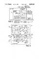
- FIG. 1is a simplified block diagram of an output buffer circuit of the present invention
- FIG. 2is a schematic circuit diagram of the output buffer circuit of FIG. 1, constructed in accordance with the principles of the present invention.
- FIGS. 3-7are schematic circuit diagrams illustrating alternative embodiments of the output buffer circuit of FIG. 2.
- FIG. 1a simplified block diagram of an output buffer circuit 10 of the present invention which has reduced ground bounce but yet maintains a high-speed of operation and has a high drive current capability.
- the output buffer circuit 10is formed of an AC buffer 12 and a DC buffer 14.
- the output buffer circuit 10provides an output signal at an output node A in response to a data input signal DATA received at a data input node B.
- the output node Ais used to drive a capacitive load as represented by the designation C L .
- the AC buffer 12is designed with small-size pull-up and pull-down output transistor devices so as to produce a high speed of operation but provides a low current drive.
- the small-size output transistor deviceswill thus have smaller transient currents, thereby minimizing the ground bounce.
- the small-size transistor devicesare designed to have fast "turn-on” and fast "turn-off” characteristics.
- the DC buffer 14is designed with large-size pull-up and pull-down output transistor devices so as to produce a slow speed of operation but has the high current drive capability.
- the large-size transistor devicesare designed to have fast "turn-off” and slow “turn-on” characteristics.
- the fast "turn-off" of the large-size transistor devicesinsure that no conflicting drive exists between the AC and DC buffers.
- the slow “turn-on” of the large-size transistor devicesfacilitates the reduction of the transient currents.
- FIG. 2there is shown a schematic circuit diagram of the output buffer circuit 10 of the present invention.
- the output buffer circuit 10 of FIG. 2provides the output signal at the output node A in response to the data input signal DATA received at the input node B, a first enable signal OE received at enable input node C, and a second enable signal OE received at enable input node D.
- the second enable signal OEis complementary to the first enable signal OE.
- the output buffer circuit 10includes the AC buffer 12 and the DC buffer 14.
- the AC buffer 12includes an N-channel MOS pull-up transistor Q1 and an N-channel MOS pull-down transistor Q2.
- the transistors Q1 and Q2have fast "turn-off” and fast "turn-on” characteristics.
- a first external power supply terminal 16is connected to a first power supply potential VCC and is further joined to an internal power supply node E via a power supply line 18 having inductance.
- a second external power supply terminal 18is connected to a second supply or ground potential GND and is further joined to an internal ground potential node F via a power supply line 20 having inductance.
- the AC buffer 12further includes inverters G1, G4 and G5, and a pair of NAND logic gates G2, G3.
- the NAND gate G2receives the first enable signal OE on line 22 and the data input signal DATA via the inverter G1 on line 24.
- the NAND gate G3receives the same first enable signal OE on line 26 and the same data input signal DATA on line 28.
- the output of the NAND gate G2is connected to the input of the inverter G4 on line 30, and the output of the inverter G4 is connected via line 32 to the gate of the pull-up transistor Q1.
- the output of the NAND gate G3is connected to the input of the inverter G5 on line 34, and the output of the inverter G5 is connected via line 36 to the gate of the pull-down transistor Q2.
- the pull-up transistor Q1has its drain connected to the internal supply node E and its source connected to the drain of the pull-down transistor Q2 and to the output node A.
- the source of the pull-down transistor Q2is connected to the internal ground node F.
- the transistors Q1 and Q2are made to be of a relatively small-size so as to have smaller transient currents, thereby reducing ground bounce.
- the DC buffer 14includes an N-channel MOS pull-up transistor Q3 and an N-channel MOS pull-down transistor Q4.
- the transistors Q3 and Q4have fast "turn-off” and slow “turn-on” characteristics.
- the DC buffer 14further includes inverters G6, G15; a first delay network 38; a second delay network 40; and a pair of NOR logic gates G11, G14.
- the NOR gate G11receives the second enable signal OE on line 42 and the same data input signal DATA on line 44.
- the data input signal DATA received at the node Bis inverted twice by the inverters G1 and G6 to produce the data input signal on the line 44.
- the NOR gate G11also receives a first delayed signal from the output of the first delay network 38.
- the input of the delay network 38is from the output of the NOR gate G14.
- the output of the NOR gate G11is connected via line 46 to the gate of the pull-up transistor Q3.
- the NOR gate G14receives the same second enable signal OE on line 48 and the same data input signal DATA on line 50 via the inverters G1, G6 and G15.
- the NOR gate G14also receives a second delayed signal from the output of the second delay network 40.
- the input to the delay network 40is from the output of the NOR gate G11.
- the output of the NOR gate G14is connected via line 52 to the gate of the pull-down transistor G4.
- the pull-up transistor Q3has its drain connected to the same internal supply node E and it source connected to the drain of the pull-down transistor Q4 and to the output node A.
- the source of the pull-down transistor Q4is connected to the same internal ground node F.
- the transistors Q3 and Q4are made to be of a relatively large-size so as to meet the high current drive requirements. In other words, the sizes of the transistors Q3 and Q4 are made to be larger in size than the transistors Q1 and Q2.
- the first delay network 38is formed of four series-connected inverters G7, G8, G9 and G10. As can be seen, the input of the inverter G7 defining the input of the delay network 38 is connected to the output of the NOR gate G14. The output of the inverter G10 defining the output of the delay network 38 is connected to one input of the NOR gate G11.
- the second delay network 40is formed of two series-connected inverters G12 and G13. The input of the inverter G12 defining the input of the delay network 40 is connected to the output of the NOR gate G11. The output of the inverter G13 defining the output of the delay network 40 is connected to one input of the NOR gate G14. It should be understood by those skilled in the art that there exists various ways in which to implement the delay networks 38 and 40.
- the pull-up action of FIG. 2will now be explained. Initially, it will be assumed that the first enable signal OE is high, the second enable signal OE is low, and the output signal at the output node is low. Thus, the pull-down transistor Q2 in the AC buffer 12 and the pull-down transistor Q4 in the DC buffer 14 are both turned on. In addition, the pull-up transistor Q1 in the AC buffer and the pull-up transistor Q3 in the DC buffer are both turned off. Further, it will be assumed that the data input signal DATA is at a high level.
- the transistor Q2When the data input signal DATA makes a high-to-low transition, the transistor Q2 is turned off quickly since the output of the inverter G5 will be low and the transistor Q1 is turned on quickly since the output of the inverter G4 will be high so as to pull the output node high. Also, the transistor Q4 will be turned off quickly since the output of the NOR gate G14 will be low. However, the transistor Q3 will be turned on slowly since the change at the output of the NOR gate G11 to a high level will be delayed by the first delay means 38. As a result, the instantaneous pull-up current generated at the internal supply node E of the present buffer circuit is reduced since it is primarily determined by the size of the transistor Q1, which has been made to be small. This minimizes the noise generated in the inductive lead line 18 between the external power supply terminal 16 and the internal supply potential node E.
- the transistor Q1When the data input signal DATA makes a low-to-high transition, the transistor Q1 is turned off quickly since the output of the inventer G4 will be low and the transistors Q2 is turned on quickly since the output of the inverter G5 will be high so as to pull down the output node A. Also, the transistor Q3 will be turned off quickly since the output of the NOR gate G11 will be low. However, the transistor Q4 will be turned on slowly since the change at the output of the NOR gate G14 to a high level will be delayed by the second delay network 40. As a result, the instantaneous pull-down current generated at the internal ground node F of the present buffer is reduced since it is primarily determined by the size of the transistor Q2, which has been made to be small. This minimizes the noise in the inductive lead line 20 between the second external power supply terminal 18 and the internal ground potential node F.
- the pull-up transistor G3 in the DC buffer 14is delayed in its turn-on with respect to the turn-on of the pull-up transistor Q1 in the AC buffer 12 when the output node A is making a low-to-high transition.
- the pull-down transistor Q4 in the DC bufferis delayed in its turn-on with respect to the turn-on of the pull-down transistor Q2 in the AC buffer when the output node A is making a high-to-low transition.
- FIGS. 3-7are schematic circuit diagrams illustrating alternative embodiments of the output buffer circuit 10 of FIG. 2.
- the output buffer circuit 10a of FIG. 3is quite similar to the buffer circuit 10 of FIG. 2, except the data input signal DATA has been changed to a data input signal DATA and the second enable signal OE is taken from the output of the inverter G6. It should also be noted that the inverter G15 in FIG. 2 has been eliminated.
- the output buffer circuit 10b of FIG. 4is quite similar to the buffer circuit 10a of FIG. 3, except the input signal to the first delay network 38 is taken from the output of the inverter G5 in the AC buffer 12 rather than from the output of the NOR gate G14 in the DC buffer 14. Similarly, the input signal to the second delay network 40 is taken from the output of the inverter G4 in the AC buffer rather than from the output of the NOR gate G11 in the DC buffer.
- the output buffer circuit 10c of FIG. 5is quite similar to the buffer circuit 10b of FIG. 4, except the data input signal DATA has been changed to a data input signal DATA.
- the connection of the inverter G1 in FIG. 5is different from that of FIG. 4.
- the output buffer circuit 10d of FIG. 6is also quite similar to the buffer circuit 10b of FIG. 4, except the second pull-up device Q3 is formed of a P-channel MOS transistor and the NOR gate G11 is replaced by a NAND gate G11a.
- the output buffer circuit 10e of FIG. 7is also quite similar to the buffer circuit 10b of FIG. 4, except the pull-up and pull-down N-channel transistors Q1-Q4 have been replaced by respective NPN-type bipolar transistors.
- the present inventionprovides an improved output buffer circuit which is formed of an AC buffer and a DC buffer.
- the output buffer circuit of the present inventionhas reduced ground bounce, but yet maintains a high speed of operation and has a high current drive capability.
Landscapes
- Physics & Mathematics (AREA)
- Engineering & Computer Science (AREA)
- Computer Hardware Design (AREA)
- Computing Systems (AREA)
- General Engineering & Computer Science (AREA)
- Mathematical Physics (AREA)
- Electronic Switches (AREA)
- Logic Circuits (AREA)
Abstract
Description
This invention relates generally to output buffer circuits and more particularly, it relates to a high-speed, high-drive output buffer circuits in integrated circuits.
As is well-known, digital logic circuits are widely used in the areas of electronics and computer-type equipment. One such use of digital logic circuits is to provide an interface function between one logic type of a first integrated circuit device and another logic type of a second integrated circuit device. An output buffer circuit is an important component for performing this interface function. The output buffer circuit generates, when enabled, an output signal which is a function of a data signal received from other logic circuitry of the integrated circuit.
Output buffer circuits typically use a pull-up transistor device and a pull-down transistor device connected in series between first and second power supply terminals. The first power supply terminal may be supplied with a positive potential VCC, which is connected to an internal power supply potential node. A second power supply terminal may be supplied with a ground potential, which is connected to an internal ground potential node. The connection point of the pull-up and pull-down devices is further joined to an output terminal.
Dependent upon the logic state of the data input signal and an enable signal, either the pull-up or pull-down transisted device is quickly turned ON and the other one of them is turned OFF. Such rapid switching ON and OFF of the pull-up and pull-down transistor devices causes sudden surges of current creating what is commonly known as current spikes. Also, during output switching, charging and discharging currents from the pull-up and pull-down transistors to the external capacitance load exist. These transient currents (current spikes and charging/discharging currents) will flow through the impedance and inductive components of power supply and ground lines so as to cause inductive noises at the internal power supply potential and the internal ground potential nodes of the output buffer.
These internal supply and ground noises are undesirable, and they will degrade the output logic "1" and logic "0" voltage levels causing interfacing problems among the output buffer circuit and other integrated circuits. This undesirable supply and ground noise is generally referred to as "ground bounce." The "ground bounce" will be more severe when more output buffers are switching simultaneously, at higher operating speed, or driving larger external capacitance loads.
In the design of output buffer circuits, it is thus seen that a trade-off exists between achieving high-speed/high-drive operation and minimizing of the ground bounce. While there have been attempts made in the prior art of output buffer design to achieve higher speed and higher output drive currents by increasing the sizes of the output pull-up and pull-down devices, this has resulted in the disadvantage of increasing the ground bounce. In other words, in order to minimize the ground bounce for prior art output buffer circuit design, the high-speed or high-drive needed to be sacrificed.
It would therefore be desirable to provide an output buffer circuit which has reduced ground bounce, but yet maintains a high speed of operation and has a high drive current capability. The output buffer circuit of the present invention includes an AC buffer and a DC buffer. The AC buffer is formed of a first pull-up transistor and a first pull-down transistor. The DC buffer is formed of a second pull-up transistor and a second pull-down transistor. The sizes of the first pull-up and pull-down transistors in the AC buffer are smaller in size than the second pull-up and pull-down transistors in the DC buffer. The reduction in ground bounce is achieved by delaying the turn-on of the second larger pull-up and pull-down transistors with respect to the first pull-up and pull-down transistors during transitions.
Accordingly, it is a general object of the present invention to provide a high-speed, high-drive output buffer circuit with reduced ground bounce which is relatively simple and economical to manufacture and assemble, but yet overcomes the disadvantages of the prior art output buffers.
It is an object of the present invention to provide a high-speed, high-drive output buffer which has a significant reduction in ground bounce.
It is another object of the present invention to provide a high-speed, high-drive output buffer circuit which includes an AC buffer and a DC buffer.
It is still another object of the present invention to provide an output buffer circuit which includes an AC buffer having small pull-up and pull-down transistor devices and a DC buffer formed of larger pull-up and pull-down transistor devices.
In accordance with these aims and objectives, the present invention is concerned with the provision of a high-speed, high-drive output buffer circuit for providing an output signal at an output node with reduced ground bounce which includes an AC buffer and a DC buffer. The AC buffer is responsive to a data input signal for generating quickly high-to-low and low-to-high transitions at the output node. The AC buffer is formed of a first pull-up transistor and a first pull-down transistor connected in series. The DC buffer is also responsive to the data input signal for generating slowly the high-to-low and low-to-high transitions at the output node. The DC buffer is formed of a second pull-up transistor and a second pull-down transistor connected in series.
The second pull-up transistor is delayed in its turn-on with respect to the first pull-up transistor when the output node is making the low-to-high transition so as to reduce the ground bounce. Similarly, the second pull-down transistor is delayed in its turn-on with respect to the first pull-down transistor when the output node is making the high-to-low transition so as to reduce the ground bounce.
These and other objects and advantages of the present invention will become more fully apparent from the following detailed description when read in conjunction with the accompanying drawings with like reference numerals indicating corresponding parts throughout, wherein:
FIG. 1 is a simplified block diagram of an output buffer circuit of the present invention;
FIG. 2 is a schematic circuit diagram of the output buffer circuit of FIG. 1, constructed in accordance with the principles of the present invention; and
FIGS. 3-7 are schematic circuit diagrams illustrating alternative embodiments of the output buffer circuit of FIG. 2.
Referring now in detail to the drawings, there is shown in FIG. 1 a simplified block diagram of anoutput buffer circuit 10 of the present invention which has reduced ground bounce but yet maintains a high-speed of operation and has a high drive current capability. Theoutput buffer circuit 10 is formed of anAC buffer 12 and aDC buffer 14. Theoutput buffer circuit 10 provides an output signal at an output node A in response to a data input signal DATA received at a data input node B. The output node A is used to drive a capacitive load as represented by the designation CL.
TheAC buffer 12 is designed with small-size pull-up and pull-down output transistor devices so as to produce a high speed of operation but provides a low current drive. The small-size output transistor devices will thus have smaller transient currents, thereby minimizing the ground bounce. The small-size transistor devices are designed to have fast "turn-on" and fast "turn-off" characteristics. TheDC buffer 14 is designed with large-size pull-up and pull-down output transistor devices so as to produce a slow speed of operation but has the high current drive capability. The large-size transistor devices are designed to have fast "turn-off" and slow "turn-on" characteristics. The fast "turn-off" of the large-size transistor devices insure that no conflicting drive exists between the AC and DC buffers. The slow "turn-on" of the large-size transistor devices facilitates the reduction of the transient currents.
In FIG. 2, there is shown a schematic circuit diagram of theoutput buffer circuit 10 of the present invention. Theoutput buffer circuit 10 of FIG. 2 provides the output signal at the output node A in response to the data input signal DATA received at the input node B, a first enable signal OE received at enable input node C, and a second enable signal OE received at enable input node D. The second enable signal OE is complementary to the first enable signal OE. Theoutput buffer circuit 10 includes theAC buffer 12 and theDC buffer 14.
TheAC buffer 12 includes an N-channel MOS pull-up transistor Q1 and an N-channel MOS pull-down transistor Q2. The transistors Q1 and Q2 have fast "turn-off" and fast "turn-on" characteristics. A first externalpower supply terminal 16 is connected to a first power supply potential VCC and is further joined to an internal power supply node E via apower supply line 18 having inductance. A second externalpower supply terminal 18 is connected to a second supply or ground potential GND and is further joined to an internal ground potential node F via apower supply line 20 having inductance.
TheAC buffer 12 further includes inverters G1, G4 and G5, and a pair of NAND logic gates G2, G3. The NAND gate G2 receives the first enable signal OE online 22 and the data input signal DATA via the inverter G1 online 24. The NAND gate G3 receives the same first enable signal OE online 26 and the same data input signal DATA online 28. The output of the NAND gate G2 is connected to the input of the inverter G4 online 30, and the output of the inverter G4 is connected vialine 32 to the gate of the pull-up transistor Q1. The output of the NAND gate G3 is connected to the input of the inverter G5 online 34, and the output of the inverter G5 is connected vialine 36 to the gate of the pull-down transistor Q2.
The pull-up transistor Q1 has its drain connected to the internal supply node E and its source connected to the drain of the pull-down transistor Q2 and to the output node A. The source of the pull-down transistor Q2 is connected to the internal ground node F. The transistors Q1 and Q2 are made to be of a relatively small-size so as to have smaller transient currents, thereby reducing ground bounce.
TheDC buffer 14 includes an N-channel MOS pull-up transistor Q3 and an N-channel MOS pull-down transistor Q4. The transistors Q3 and Q4 have fast "turn-off" and slow "turn-on" characteristics. TheDC buffer 14 further includes inverters G6, G15; afirst delay network 38; asecond delay network 40; and a pair of NOR logic gates G11, G14.
The NOR gate G11 receives the second enable signal OE online 42 and the same data input signal DATA online 44. The data input signal DATA received at the node B is inverted twice by the inverters G1 and G6 to produce the data input signal on theline 44. The NOR gate G11 also receives a first delayed signal from the output of thefirst delay network 38. The input of thedelay network 38 is from the output of the NOR gate G14. The output of the NOR gate G11 is connected vialine 46 to the gate of the pull-up transistor Q3.
The NOR gate G14 receives the same second enable signal OE online 48 and the same data input signal DATA online 50 via the inverters G1, G6 and G15. The NOR gate G14 also receives a second delayed signal from the output of thesecond delay network 40. The input to thedelay network 40 is from the output of the NOR gate G11. The output of the NOR gate G14 is connected vialine 52 to the gate of the pull-down transistor G4.
The pull-up transistor Q3 has its drain connected to the same internal supply node E and it source connected to the drain of the pull-down transistor Q4 and to the output node A. The source of the pull-down transistor Q4 is connected to the same internal ground node F. The transistors Q3 and Q4 are made to be of a relatively large-size so as to meet the high current drive requirements. In other words, the sizes of the transistors Q3 and Q4 are made to be larger in size than the transistors Q1 and Q2.
Thefirst delay network 38 is formed of four series-connected inverters G7, G8, G9 and G10. As can be seen, the input of the inverter G7 defining the input of thedelay network 38 is connected to the output of the NOR gate G14. The output of the inverter G10 defining the output of thedelay network 38 is connected to one input of the NOR gate G11. Thesecond delay network 40 is formed of two series-connected inverters G12 and G13. The input of the inverter G12 defining the input of thedelay network 40 is connected to the output of the NOR gate G11. The output of the inverter G13 defining the output of thedelay network 40 is connected to one input of the NOR gate G14. It should be understood by those skilled in the art that there exists various ways in which to implement thedelay networks
In order to provide an understanding of the operation of the present invention, the pull-up action of FIG. 2 will now be explained. Initially, it will be assumed that the first enable signal OE is high, the second enable signal OE is low, and the output signal at the output node is low. Thus, the pull-down transistor Q2 in theAC buffer 12 and the pull-down transistor Q4 in theDC buffer 14 are both turned on. In addition, the pull-up transistor Q1 in the AC buffer and the pull-up transistor Q3 in the DC buffer are both turned off. Further, it will be assumed that the data input signal DATA is at a high level.
When the data input signal DATA makes a high-to-low transition, the transistor Q2 is turned off quickly since the output of the inverter G5 will be low and the transistor Q1 is turned on quickly since the output of the inverter G4 will be high so as to pull the output node high. Also, the transistor Q4 will be turned off quickly since the output of the NOR gate G14 will be low. However, the transistor Q3 will be turned on slowly since the change at the output of the NOR gate G11 to a high level will be delayed by the first delay means 38. As a result, the instantaneous pull-up current generated at the internal supply node E of the present buffer circuit is reduced since it is primarily determined by the size of the transistor Q1, which has been made to be small. This minimizes the noise generated in theinductive lead line 18 between the externalpower supply terminal 16 and the internal supply potential node E.
The pull-down action of FIG. 2 will now be described. Assume that the data input signal DATA is at a low level and that the output signal at the output node A is high. Accordingly, the pull-up transistor Q1 in theAC buffer 12 and the pull-up transistor Q3 in theDC buffer 14 are both turned on. In addition, the pull-down transistor Q2 in the AC buffer and the pull-down transistor Q4 in the DC buffer are both turned off.
When the data input signal DATA makes a low-to-high transition, the transistor Q1 is turned off quickly since the output of the inventer G4 will be low and the transistors Q2 is turned on quickly since the output of the inverter G5 will be high so as to pull down the output node A. Also, the transistor Q3 will be turned off quickly since the output of the NOR gate G11 will be low. However, the transistor Q4 will be turned on slowly since the change at the output of the NOR gate G14 to a high level will be delayed by thesecond delay network 40. As a result, the instantaneous pull-down current generated at the internal ground node F of the present buffer is reduced since it is primarily determined by the size of the transistor Q2, which has been made to be small. This minimizes the noise in theinductive lead line 20 between the second externalpower supply terminal 18 and the internal ground potential node F.
When the first enable signal OE is at the low or logic "0" level, the outputs of both inverters G4 and G5 are at the logic "0", causing both the N-channel transistors Q1 and Q2 to be turned off. Further, since the second enable signal OE is at the high or logic "1" level, the outputs of both NOR gates G11 and G14 are at the logic "0" level, causing both the N-channel transistors Q3 and Q4 to be turned off. This produces a high impedance tri-state mode at the output node A in which theoutput buffer circuit 10 is not enabled.
As can be seen, the pull-up transistor G3 in theDC buffer 14 is delayed in its turn-on with respect to the turn-on of the pull-up transistor Q1 in theAC buffer 12 when the output node A is making a low-to-high transition. Similarly, the pull-down transistor Q4 in the DC buffer is delayed in its turn-on with respect to the turn-on of the pull-down transistor Q2 in the AC buffer when the output node A is making a high-to-low transition. As a consequence, the ground bounce due to the inductance in the power supply lines is reduced significantly.
FIGS. 3-7 are schematic circuit diagrams illustrating alternative embodiments of theoutput buffer circuit 10 of FIG. 2. Theoutput buffer circuit 10a of FIG. 3 is quite similar to thebuffer circuit 10 of FIG. 2, except the data input signal DATA has been changed to a data input signal DATA and the second enable signal OE is taken from the output of the inverter G6. It should also be noted that the inverter G15 in FIG. 2 has been eliminated.
The output buffer circuit 10b of FIG. 4 is quite similar to thebuffer circuit 10a of FIG. 3, except the input signal to thefirst delay network 38 is taken from the output of the inverter G5 in theAC buffer 12 rather than from the output of the NOR gate G14 in theDC buffer 14. Similarly, the input signal to thesecond delay network 40 is taken from the output of the inverter G4 in the AC buffer rather than from the output of the NOR gate G11 in the DC buffer.
The output buffer circuit 10c of FIG. 5 is quite similar to the buffer circuit 10b of FIG. 4, except the data input signal DATA has been changed to a data input signal DATA. Thus, the connection of the inverter G1 in FIG. 5 is different from that of FIG. 4. Theoutput buffer circuit 10d of FIG. 6 is also quite similar to the buffer circuit 10b of FIG. 4, except the second pull-up device Q3 is formed of a P-channel MOS transistor and the NOR gate G11 is replaced by a NAND gate G11a. Finally, theoutput buffer circuit 10e of FIG. 7 is also quite similar to the buffer circuit 10b of FIG. 4, except the pull-up and pull-down N-channel transistors Q1-Q4 have been replaced by respective NPN-type bipolar transistors.
From the foregoing detailed description, it can thus be seen that the present invention provides an improved output buffer circuit which is formed of an AC buffer and a DC buffer. The output buffer circuit of the present invention has reduced ground bounce, but yet maintains a high speed of operation and has a high current drive capability.
While there has been illustrated and described what is at present considered to be a preferred embodiment of the present invention, it will be understood by those skilled in the art that various changes and modifications may be made, and equivalents may be substituted for elements thereof without departing from the true scope of the invention. In addition, many modifications may be made to adapt a particular situation or material to the teachings of the invention without departing from the central scope thereof. Therefore, it is intended that this invention not be limited to the particular embodiment disclosed as the best mode contemplated for carrying out the invention, but that the invention will include all embodiments falling within the scope of the appended claims.
Claims (17)
1. A high-speed, high-drive output buffer circuit for producing an output signal at an output node with reduced ground bounce, comprising:
AC buffer means (12) responsive to a data input signal for generating quickly high-to-low and low-to-high transitions at the output node;
said AC buffer means (12) including a first pull-up transistor (Q1) and a first pull-down transistor (Q2) connected in series, said first pull-up transistor (Q1) having one of its main electrodes coupled to a first power supply terminal and its other main electrode coupled to the output node, said first pull-down transistor (Q2) having one of its main electrodes coupled to a second power supply terminal and its other main electrode coupled to the output node;
said AC buffer means (12) further including a first NAND logic gate (G2), a second NAND logic gate (G3), a first inverter (G1), a second inverter (G4), and a third inverter (G5);
said first inverter (G1) having its input connected to the data input signal and its output connected to a first input of said first NAND gate (G2), said first NAND gate (G2) having a second input connected to a first enable signal, said first NAND gate (G2) having its output connected to the input of said second inverter (G4);
said second NAND gate (G3) having a first input connected to the data input signal and a second input connected to the first enable signal, said second NAND gate (G3) having its output connected to the input of said third inverter (G5);
said second inverter (G4) having its output connected to a control electrode of said first pull-up transistor (Q1) and said third inverter (G5) having its output connected to a control electrode of said first pull-down transistor (Q2);
DC buffer means (14) responsive to the data input signal for generating slowly high-to-low and low-to-high transitions at the output node;
said DC buffer means (14) including a second pull-up transistor (Q3) and a second pull-down transistor (Q4) connected in series, said second pull-up transistor (Q3) having one of its main electrodes coupled to the first power supply terminal and its other main electrode coupled to the output node, said second pull-down transistor (G4) having one of its main electrodes coupled to the second power supply terminal and its other main electrode coupled to the output node;
said DC buffer means (14) further including a first delay means (38) having an input and an output, a second delay means (40) having an input and an output, a first NOR logic gate (G11), a second NOR logic gate (G14), a fourth inverter (G6), and a fifth inverter (G15);
said first NOR logic gate (G11) having a first input connected to the output of said fourth inverter (G6), a second input connected to the output of said first delay means (38), and a third input connected to a second enable signal;
said second NOR logic gate (G14) having a first input connected to the output of said fifth inverter (G15), a second input connected to the output of said second delay means (40), and a third input connected to the second enable signal;
said fourth inverter (G6) having its input connected to the output of said first inverter (G1) in said AC buffer means (12) and said fifth inverter (G15) having its input connected to the output of said fourth inverter (G6); and
said first NOR gate (G11) having its output connected to the input of said second delay means (40) and to a control electrode of said second pull-up transistor (Q3), said second NOR gate (G14) having its output connected to the input of said first delay means (38) and to a control electrode of said second pull-down transistor (Q4).
2. A high-speed, high-drive output buffer circuit as claimed in claim 1, wherein said first pull-up transistor (Q1) is an N-channel MOS transistor.
3. A high-speed, high-drive output buffer circuit as claimed in claim 2, wherein said first pull-down transistor (Q2) is an N-channel MOS transistor.
4. A high-speed, high-drive output buffer circuit as claimed in claim 3, wherein said second pull-up transistor (Q3) is an N-channel MOS transistor.
5. A high-speed, high-drive output buffer circuit as claimed in claim 4, wherein said second pull-down transistor (Q4) is an N-channel MOS transistor.
6. A high-speed, high-drive output buffer circuit as claimed in claim 1, wherein said first delay means (38) comprises a first delay network formed of four series-connected inverters (G7, G8, G9, G10).
7. A high-speed, high-drive output buffer circuit as claimed in claim 6, wherein said second delay means (40) comprises a second delay network formed of two series-connected inverters (G12, G13).
8. A high-speed, high-drive output buffer circuit as claimed in claim 1, wherein said second pull-up transistor (Q3) is delayed in its turn-on with respect to the turn-on of said first pull-up transistor (Q1) when the output node is making the low-to-high transition so as to reduce the ground bounce.
9. A high-speed, high-drive output buffer circuit as claimed in claim 8, wherein said second pull-down transistor (Q4) is delayed in its turn-on with respect to the turn-on of said first pull-down transistor (Q2) when the output node is making the high-to-low transition so as to reduce the ground bounce.
10. A high-speed, high drive output buffer circuit for producing an output signal at an output node with reduced ground bounce, comprising:
AC buffer means (12) responsive to a data input signal for generating quickly high-to-low and low-to-high transitions at the output node;
said AC buffer means (12) including a first pull-up transistor (Q1) and a first pull-down transistor (Q2) connected in series, said first pull-up transistor (Q1) having one of its main electrodes coupled to a first power supply terminal and its other main electrode coupled to the output node, said first pull-down transistor (Q2) having one of its main electrodes coupled to a second power supply terminal and its other main electrode coupled to the output node;
said AC buffer means (12) further including a first NAND logic gate (G2), a second NAND logic gate (G3), a first inverter (G1), a second inverter (G4), and a third inverter (G5);
said first inverter (G1) having its input connected to the data input signal and its output connected to a first input of said second NAND gate (G3), said second NAND gate (G3) having a second input connected to an enable signal, said second NAND gate (G3) having its output connected to the input of said third inverter (G5);
said first NAND gate (G2) having a first input connected to the data input signal and a second input connected to the enable signal, said first NAND gate (G2) having its output connected to the input of said second inverter (G4);
said second inverter (G4) having its output connected to a control electrode of said first pull-up transistor (Q1) and said third inverter (G5) having its output connected to a control electrode of said first pull-down transistor (Q2);
DC buffer means (14) responsive to the data input signal for generating slowly high-to-low and low-to-high transitions at the output node;
said DC buffer means (14) including a second pull-up transistor (Q3) and a second pull-down transistor (Q4) connected in series, said second pull-up transistor (Q3) having one of its main electrodes coupled to the first power supply terminal and its other main electrode coupled to the output node, said second pull-down transistor (G4) having one of its main electrodes coupled to the second power supply terminal and its other main electrode coupled to the output node;
said DC buffer means (14) further including a first delay means (38) having an input and an output, a second delay means (40) having an input and an output, a first NOR logic gate (G11), a second NOR logic gate (G14), and a fourth inverter (G6);
said first NOR logic gate (G11) having a first input connected to the output of said fourth inverter (G6), a second input connected to the output of said first delay means (38), and a third input connected to the output of said first inverter (G1);
said second NOR logic gate (G14) having a first input connected to the output of said fourth inverter (G6), a second input connected to the output of said second delay means (40), and a third input connected to the data input signal;
said fourth inverter (G6) having its input connected to the enable signal;
said first NOR gate (G11) having its output connected to a control electrode of said second pull-up transistor (Q3), said second NOR gate (G14) having its output connected to a control electrode of said second pull-down transistor (Q4);
said input of said first delay means (38) being connected to one of said outputs of said second NOR gate (G14) and said third inverter (G5) in said AC buffer means (12);
said input of said second delay means (40) being connected to one of said outputs of said first NOR gate (G11) and said second inverter (G4) in said AC buffer means (12);
said first delay means (38) delaying the turn-on of said second pull-up transistor (Q3) with respect to the turn-on of said first pull-up transistor (Q1) when the output node is making the low-to-high transition so as to reduce the ground bounce; and
said second delay means (40) delaying the turn-on of said second pull-down transistor (Q4) with respect to the turn-on of said first pull-down transistor (Q2) when the output node is making the high-to-low transition so as to reduce the ground bounce.
11. A high-speed, high-drive output buffer circuit as claimed in claim 10, wherein said first pull-up transistor (Q1) is an N-channel MOS transistor.
12. A high-speed, high-drive output buffer circuit as claimed in claim 11, wherein said first pull-down transistor (Q2) is an N-channel MOS transistor.
13. A high-speed, high-drive output buffer circuit as claimed in claim 12, wherein said second pull-up transistor (Q3) is an N-channel MOS transistor.
14. A high-speed, high-drive output buffer circuit as claimed in claim 13, wherein said second pull-down transistor (Q4) is an N-channel MOS transistor.
15. A high-speed, high-drive output buffer circuit as claimed in claim 10, wherein said first delay means (38) comprises a first delay network formed of four series-connected inverters (G7, G8, G9, G10).
16. A high-speed, high-drive output buffer circuit as claimed in claim 15, wherein said second delay means (40) comprises a second delay network formed of two series-connected inverters (G12, G13).
17. A high-speed, high-drive output buffer circuit for providing an output signal at an output node with reduced ground bounce, comprising:
AC buffer means (912) formed of a first pullup transistor (Q1) and a first pull-down transistor (Q2) connected in series and being responsive to a data input signal for generating quickly high-to-low and low-to high transitions at the output node;
said AC buffer means (12) further including a first NAND logic gate (G2), a second NAND logic gate (G3), a first inverter (G1), a second inverter (G4) and a third inverter (G5);
said first inverter (G1) having its input connected to the data input signal and its output connected to a first input of said first NAND gate (G2), said first NAND gate (G2) having a second input connected to an enable signal, said first NAND gate (G2) having its output connected to the input of said second inverter (G4);
said second NAND gate (G3) having a first input connected to the data input signal and a second input connected to the enable signal, said second NAND gate (G3) having its output connected to the input of said third inverter (G5);
said second inverter (G4) having its output connected to a control electrode of said first pull-up transistor (Q1) and said third inverter (G5) having its output connected to a control electrode of said first pull-down transistor (Q2);
DC buffer means (14) being formed of a second pull-up transistor (Q3) and a second pull-down transistor (Q4) connected in series and being responsive to the data input signal for generating slowly high-to-low and low-to-high transitions at the output node;
said DC buffer means (14) further including a first delay means (38) having an input and an output, a second delay means (40) having an input and an output, a first NOR logic gate (G11), a second NOR logic gate (G14), and a fourth inverter (G6);
said first NOR logic gate (G11) having a first input connected to the output of said fourth inverter (G6), a second input connected to the output of said first delay means (38), and a third input connected to the data input signal;
said second NOR logic gate (G14) having a first input connected to the output of said fourth inverter (G6), a second input connected to the output of said second delay means (40), and a third input connected to the output of said first inverter (G1);
said fourth inverter (G6) having its input connected to the enable signal;
said first NOR gate (G11) having its output connected to a control electrode of said second pull-up transistor (Q3), said second NOR gate (G14) having its output connected to a control electrode of said second pull-down transistor (Q4);
said input of said first delay means (38) being connected to said output of said third inverter (G5) in said AC buffer means (12);
said input of said second delay means (40) being connected to said output of said second inverter (G4) in said AC buffer means (12);
said first delay means (38) delaying the turn-on of said second pull-up transistor (Q3) with respect to the turn-on of said first pull-up transistor (Q1) when the output node is making the low-to-high transition so as to reduce the ground bounce;
said second delay means (40) delaying the turn-on of said second pull-down transistor (Q4) with respect to the turn-on of said first pulldown transistor (Q2) when the output node is making the high-to-low transition so as to reduce the ground bounce; and
the sizes of said first pull-up and pull down transistors (Q1, Q2) in the AC buffer means (12) being smaller in size than said second pull-up and pull-down transistors (Q3, Q4) in said DC buffer means (14).
Priority Applications (1)
| Application Number | Priority Date | Filing Date | Title |
|---|---|---|---|
| US07/148,789US4820942A (en) | 1988-01-27 | 1988-01-27 | High-speed, high-drive output buffer circuits with reduced ground bounce |
Applications Claiming Priority (1)
| Application Number | Priority Date | Filing Date | Title |
|---|---|---|---|
| US07/148,789US4820942A (en) | 1988-01-27 | 1988-01-27 | High-speed, high-drive output buffer circuits with reduced ground bounce |
Publications (1)
| Publication Number | Publication Date |
|---|---|
| US4820942Atrue US4820942A (en) | 1989-04-11 |
Family
ID=22527393
Family Applications (1)
| Application Number | Title | Priority Date | Filing Date |
|---|---|---|---|
| US07/148,789Expired - LifetimeUS4820942A (en) | 1988-01-27 | 1988-01-27 | High-speed, high-drive output buffer circuits with reduced ground bounce |
Country Status (1)
| Country | Link |
|---|---|
| US (1) | US4820942A (en) |
Cited By (57)
| Publication number | Priority date | Publication date | Assignee | Title |
|---|---|---|---|---|
| US4914318A (en)* | 1988-12-30 | 1990-04-03 | Intel Corporation | Latch circuit for a programmable logic device using dual n-type transistors |
| US4916385A (en)* | 1987-11-02 | 1990-04-10 | Mitsubishi Denki Kkabushiki Kaisha | Inverter circuit |
| EP0340731A3 (en)* | 1988-05-02 | 1990-05-23 | Kabushiki Kaisha Toshiba | Output circuit of semiconductor integrated circuit with reduced power source line noise |
| US4953130A (en)* | 1988-06-27 | 1990-08-28 | Texas Instruments, Incorporated | Memory circuit with extended valid data output time |
| US4959565A (en)* | 1989-02-10 | 1990-09-25 | National Semiconductor Corporation | Output buffer with ground bounce control |
| US4963766A (en)* | 1989-06-28 | 1990-10-16 | Digital Equipment Corporation | Low-voltage CMOS output buffer |
| US4975598A (en)* | 1988-12-21 | 1990-12-04 | Intel Corporation | Temperature, voltage, and process compensated output driver |
| US4975599A (en)* | 1989-07-26 | 1990-12-04 | International Business Machines Corporation | Method and resulting devices for compensating for process variables in a CMOS device driver circuit |
| US5001369A (en)* | 1990-07-02 | 1991-03-19 | Micron Technology, Inc. | Low noise output buffer circuit |
| US5034637A (en)* | 1989-02-17 | 1991-07-23 | Texas Instruments Deutschland Gmbh | Push-pull output stage of integrated circuit for reducing ground bounce noise |
| US5036232A (en)* | 1989-02-17 | 1991-07-30 | Texas Instruments Deutschland Gmbh | Push-pull output stage of integrated circuit providing enhanced high-low voltage level signal transition with ground bounce control |
| US5047673A (en)* | 1989-02-03 | 1991-09-10 | Nec Corporation | High speed output structure suitable for wired-OR structure |
| US5063308A (en)* | 1988-12-21 | 1991-11-05 | Intel Corporation | Output driver with static and transient parts |
| US5066872A (en)* | 1990-06-11 | 1991-11-19 | Texas Instruments Incorporated | Speed-up technique for a constant di/dt buffer |
| US5073727A (en)* | 1988-06-17 | 1991-12-17 | Harumi Shizu | Cmos inverter with noise reduction feedback means |
| US5089722A (en)* | 1990-04-02 | 1992-02-18 | Motorola, Inc. | High speed output buffer circuit with overlap current control |
| US5097152A (en)* | 1988-11-04 | 1992-03-17 | Mitsubishi Denki Kabushiki Kaisha | Buffer circuit used in a semiconductor device operating by different supply potentials and method of operating the same |
| US5097149A (en)* | 1990-07-02 | 1992-03-17 | Micron Technology, Inc. | Two stage push-pull output buffer circuit with control logic feedback for reducing crossing current, switching noise and the like |
| US5111076A (en)* | 1990-09-05 | 1992-05-05 | Min Ming Tarng | Digital superbuffer |
| US5111064A (en)* | 1990-09-05 | 1992-05-05 | Vlsi Technology, Inc. | Slow ramp high drive output pad |
| US5117129A (en)* | 1990-10-16 | 1992-05-26 | International Business Machines Corporation | Cmos off chip driver for fault tolerant cold sparing |
| US5121013A (en)* | 1990-02-12 | 1992-06-09 | Advanced Micro Devices, Inc. | Noise reducing output buffer circuit with feedback path |
| US5136179A (en)* | 1988-10-31 | 1992-08-04 | Teledyne Industries, Inc. | Logic level discriminator |
| US5146111A (en)* | 1991-04-10 | 1992-09-08 | International Business Machines Corporation | Glitch-proof powered-down on chip receiver with non-overlapping outputs |
| US5153450A (en)* | 1991-07-16 | 1992-10-06 | Samsung Semiconductor, Inc. | Programmable output drive circuit |
| EP0509489A1 (en)* | 1991-04-15 | 1992-10-21 | Oki Electric Industry Co., Ltd. | Semiconductor integrated circuit with low-noise output buffers |
| EP0511643A1 (en)* | 1991-04-30 | 1992-11-04 | Kabushiki Kaisha Toshiba | Output buffer circuit |
| US5184032A (en)* | 1991-04-25 | 1993-02-02 | Texas Instruments Incorporated | Glitch reduction in integrated circuits, systems and methods |
| US5210715A (en)* | 1988-06-27 | 1993-05-11 | Texas Instruments Incorporated | Memory circuit with extended valid data output time |
| US5268868A (en)* | 1987-09-16 | 1993-12-07 | Hitachi, Ltd. | Output buffer circuits for reducing ground bounce noise |
| US5270585A (en)* | 1992-07-27 | 1993-12-14 | Motorola, Inc. | Output driver stage with two tier current limit protection |
| US5319260A (en)* | 1991-07-23 | 1994-06-07 | Standard Microsystems Corporation | Apparatus and method to prevent the disturbance of a quiescent output buffer caused by ground bounce or by power bounce induced by neighboring active output buffers |
| US5331220A (en)* | 1993-02-12 | 1994-07-19 | Xilinx, Inc. | Soft wakeup output buffer |
| US5362996A (en)* | 1992-06-10 | 1994-11-08 | Intel Corporation | Staggered output circuit for noise reduction |
| EP0532373A3 (en)* | 1991-08-09 | 1995-01-11 | Fujitsu Ltd | |
| US5387824A (en)* | 1989-12-01 | 1995-02-07 | Vlsi Technology, Inc. | Variable drive output buffer circuit |
| US5406513A (en)* | 1993-02-05 | 1995-04-11 | The University Of New Mexico | Mechanism for preventing radiation induced latch-up in CMOS integrated circuits |
| US5418473A (en)* | 1992-10-28 | 1995-05-23 | Idaho Research Foundation, Inc. | Single event upset immune logic family |
| US5426376A (en)* | 1993-04-23 | 1995-06-20 | Vlsi Technology, Inc. | Noise isolated I/O buffer that uses two separate power supplies |
| US5428303A (en)* | 1994-05-20 | 1995-06-27 | National Semiconductor Corporation | Bias generator for low ground bounce output driver |
| US5430335A (en)* | 1991-05-15 | 1995-07-04 | Oki Electric Industry Co., Ltd. | Simplified low-noise output buffer circuit |
| US5517130A (en)* | 1994-12-20 | 1996-05-14 | Sun Microsystems, Inc. | Method and structure for reducing noise in output buffer circuits |
| EP0735676A1 (en)* | 1995-03-29 | 1996-10-02 | Hewlett-Packard Company | Predriver circuit for high current loads |
| EP0616430A3 (en)* | 1993-03-19 | 1997-06-04 | Advanced Micro Devices Inc | Buffer circuit. |
| US5852579A (en)* | 1997-06-19 | 1998-12-22 | Cypress Semiconductor Corporation | Method and circuit for preventing and/or inhibiting contention in a system employing a random access memory |
| US5859552A (en)* | 1995-10-06 | 1999-01-12 | Lsi Logic Corporation | Programmable slew rate control circuit for output buffer |
| US5877647A (en)* | 1995-10-16 | 1999-03-02 | Texas Instruments Incorporated | CMOS output buffer with slew rate control |
| US6040729A (en)* | 1997-08-25 | 2000-03-21 | Motorola, Inc. | Digital output buffer for multiple voltage system |
| US6091259A (en)* | 1997-08-29 | 2000-07-18 | Sun Microsystems, Inc. | Apparatus for accelerating digital signal transitions using a transition acceleration circuit and a transition termination circuit |
| US6208195B1 (en) | 1991-03-18 | 2001-03-27 | Integrated Device Technology, Inc. | Fast transmission gate switch |
| US6215350B1 (en) | 1991-03-18 | 2001-04-10 | Integrated Device Technology, Inc. | Fast transmission gate switch |
| US6445212B1 (en)* | 2001-01-12 | 2002-09-03 | Faraday Technology Corp. | High-speed, low-noise, impedance-matched output buffer circuit |
| US20050140430A1 (en)* | 2003-12-31 | 2005-06-30 | Wang Bonnie I. | Programmable AC current booster for faster edge-rate output in high speed applications |
| US20100156504A1 (en)* | 2006-06-30 | 2010-06-24 | Masleid Robert P | Cross point switch |
| US20110019763A1 (en)* | 2005-07-29 | 2011-01-27 | Synopsys, Inc. | USB 2.0 HS Voltage-Mode Transmitter With Tuned Termination Resistance |
| US10614864B1 (en) | 2019-05-13 | 2020-04-07 | Winbond Electronics Corp. | Buffer output circuit, driving method thereof and memory apparatus |
| US20250210099A1 (en)* | 2023-12-20 | 2025-06-26 | Qualcomm Incorporated | Dynamic transmitter calibration |
Citations (7)
| Publication number | Priority date | Publication date | Assignee | Title |
|---|---|---|---|---|
| US4251740A (en)* | 1978-11-20 | 1981-02-17 | Honeywell Inc. | Continuous focus proportional controller |
| US4508981A (en)* | 1982-06-28 | 1985-04-02 | International Business Machines Corporation | Driver circuitry for reducing on-chip Delta-I noise |
| US4527077A (en)* | 1981-06-30 | 1985-07-02 | Fujitsu Limited | Output circuit of a semiconductor device |
| JPS61167220A (en)* | 1985-01-19 | 1986-07-28 | Sanyo Electric Co Ltd | Signal output circuit |
| US4613771A (en)* | 1984-04-18 | 1986-09-23 | Burroughs Corporation | Integrated circuit having three power bases and proportioned parasitic resistive and capacitive coupling to reduce output noise |
| JPS6276924A (en)* | 1985-09-30 | 1987-04-09 | Toshiba Corp | Logic circuit output buffer device |
| GB2184622A (en)* | 1985-12-23 | 1987-06-24 | Philips Nv | Output buffer having limited rate-of-change of output current |
- 1988
- 1988-01-27USUS07/148,789patent/US4820942A/ennot_activeExpired - Lifetime
Patent Citations (7)
| Publication number | Priority date | Publication date | Assignee | Title |
|---|---|---|---|---|
| US4251740A (en)* | 1978-11-20 | 1981-02-17 | Honeywell Inc. | Continuous focus proportional controller |
| US4527077A (en)* | 1981-06-30 | 1985-07-02 | Fujitsu Limited | Output circuit of a semiconductor device |
| US4508981A (en)* | 1982-06-28 | 1985-04-02 | International Business Machines Corporation | Driver circuitry for reducing on-chip Delta-I noise |
| US4613771A (en)* | 1984-04-18 | 1986-09-23 | Burroughs Corporation | Integrated circuit having three power bases and proportioned parasitic resistive and capacitive coupling to reduce output noise |
| JPS61167220A (en)* | 1985-01-19 | 1986-07-28 | Sanyo Electric Co Ltd | Signal output circuit |
| JPS6276924A (en)* | 1985-09-30 | 1987-04-09 | Toshiba Corp | Logic circuit output buffer device |
| GB2184622A (en)* | 1985-12-23 | 1987-06-24 | Philips Nv | Output buffer having limited rate-of-change of output current |
Cited By (68)
| Publication number | Priority date | Publication date | Assignee | Title |
|---|---|---|---|---|
| US5268868A (en)* | 1987-09-16 | 1993-12-07 | Hitachi, Ltd. | Output buffer circuits for reducing ground bounce noise |
| US4916385A (en)* | 1987-11-02 | 1990-04-10 | Mitsubishi Denki Kkabushiki Kaisha | Inverter circuit |
| EP0340731A3 (en)* | 1988-05-02 | 1990-05-23 | Kabushiki Kaisha Toshiba | Output circuit of semiconductor integrated circuit with reduced power source line noise |
| US5128567A (en)* | 1988-05-02 | 1992-07-07 | Kabushiki Kaisha Toshiba | Output circuit of semiconductor integrated circuit with reduced power source line noise |
| US5073727A (en)* | 1988-06-17 | 1991-12-17 | Harumi Shizu | Cmos inverter with noise reduction feedback means |
| US5210715A (en)* | 1988-06-27 | 1993-05-11 | Texas Instruments Incorporated | Memory circuit with extended valid data output time |
| US4953130A (en)* | 1988-06-27 | 1990-08-28 | Texas Instruments, Incorporated | Memory circuit with extended valid data output time |
| US5136179A (en)* | 1988-10-31 | 1992-08-04 | Teledyne Industries, Inc. | Logic level discriminator |
| US5097152A (en)* | 1988-11-04 | 1992-03-17 | Mitsubishi Denki Kabushiki Kaisha | Buffer circuit used in a semiconductor device operating by different supply potentials and method of operating the same |
| US5063308A (en)* | 1988-12-21 | 1991-11-05 | Intel Corporation | Output driver with static and transient parts |
| US4975598A (en)* | 1988-12-21 | 1990-12-04 | Intel Corporation | Temperature, voltage, and process compensated output driver |
| US4914318A (en)* | 1988-12-30 | 1990-04-03 | Intel Corporation | Latch circuit for a programmable logic device using dual n-type transistors |
| US5047673A (en)* | 1989-02-03 | 1991-09-10 | Nec Corporation | High speed output structure suitable for wired-OR structure |
| US4959565A (en)* | 1989-02-10 | 1990-09-25 | National Semiconductor Corporation | Output buffer with ground bounce control |
| US5034637A (en)* | 1989-02-17 | 1991-07-23 | Texas Instruments Deutschland Gmbh | Push-pull output stage of integrated circuit for reducing ground bounce noise |
| US5036232A (en)* | 1989-02-17 | 1991-07-30 | Texas Instruments Deutschland Gmbh | Push-pull output stage of integrated circuit providing enhanced high-low voltage level signal transition with ground bounce control |
| US4963766A (en)* | 1989-06-28 | 1990-10-16 | Digital Equipment Corporation | Low-voltage CMOS output buffer |
| US4975599A (en)* | 1989-07-26 | 1990-12-04 | International Business Machines Corporation | Method and resulting devices for compensating for process variables in a CMOS device driver circuit |
| US5387824A (en)* | 1989-12-01 | 1995-02-07 | Vlsi Technology, Inc. | Variable drive output buffer circuit |
| US5121013A (en)* | 1990-02-12 | 1992-06-09 | Advanced Micro Devices, Inc. | Noise reducing output buffer circuit with feedback path |
| US5089722A (en)* | 1990-04-02 | 1992-02-18 | Motorola, Inc. | High speed output buffer circuit with overlap current control |
| US5066872A (en)* | 1990-06-11 | 1991-11-19 | Texas Instruments Incorporated | Speed-up technique for a constant di/dt buffer |
| US5097149A (en)* | 1990-07-02 | 1992-03-17 | Micron Technology, Inc. | Two stage push-pull output buffer circuit with control logic feedback for reducing crossing current, switching noise and the like |
| US5001369A (en)* | 1990-07-02 | 1991-03-19 | Micron Technology, Inc. | Low noise output buffer circuit |
| US5111076A (en)* | 1990-09-05 | 1992-05-05 | Min Ming Tarng | Digital superbuffer |
| US5111064A (en)* | 1990-09-05 | 1992-05-05 | Vlsi Technology, Inc. | Slow ramp high drive output pad |
| US5117129A (en)* | 1990-10-16 | 1992-05-26 | International Business Machines Corporation | Cmos off chip driver for fault tolerant cold sparing |
| US6556063B2 (en) | 1991-03-18 | 2003-04-29 | Integrated Device Technology, Inc. | Fast transmission gate switch |
| US6215350B1 (en) | 1991-03-18 | 2001-04-10 | Integrated Device Technology, Inc. | Fast transmission gate switch |
| US6208195B1 (en) | 1991-03-18 | 2001-03-27 | Integrated Device Technology, Inc. | Fast transmission gate switch |
| US5146111A (en)* | 1991-04-10 | 1992-09-08 | International Business Machines Corporation | Glitch-proof powered-down on chip receiver with non-overlapping outputs |
| EP0509489A1 (en)* | 1991-04-15 | 1992-10-21 | Oki Electric Industry Co., Ltd. | Semiconductor integrated circuit with low-noise output buffers |
| US5184032A (en)* | 1991-04-25 | 1993-02-02 | Texas Instruments Incorporated | Glitch reduction in integrated circuits, systems and methods |
| EP0511643A1 (en)* | 1991-04-30 | 1992-11-04 | Kabushiki Kaisha Toshiba | Output buffer circuit |
| US5321326A (en)* | 1991-04-30 | 1994-06-14 | Kabushiki Kaisha Toshiba | Output buffer circuit |
| US5430335A (en)* | 1991-05-15 | 1995-07-04 | Oki Electric Industry Co., Ltd. | Simplified low-noise output buffer circuit |
| US5319258A (en)* | 1991-07-16 | 1994-06-07 | Samsung Semiconductor, Inc. | Programmable output drive circuit |
| US5153450A (en)* | 1991-07-16 | 1992-10-06 | Samsung Semiconductor, Inc. | Programmable output drive circuit |
| US5319260A (en)* | 1991-07-23 | 1994-06-07 | Standard Microsystems Corporation | Apparatus and method to prevent the disturbance of a quiescent output buffer caused by ground bounce or by power bounce induced by neighboring active output buffers |
| US5517129A (en)* | 1991-08-09 | 1996-05-14 | Fujitsu Limited | High-speed dual-buffered output circuit |
| EP0532373A3 (en)* | 1991-08-09 | 1995-01-11 | Fujitsu Ltd | |
| US5362996A (en)* | 1992-06-10 | 1994-11-08 | Intel Corporation | Staggered output circuit for noise reduction |
| US5270585A (en)* | 1992-07-27 | 1993-12-14 | Motorola, Inc. | Output driver stage with two tier current limit protection |
| US5418473A (en)* | 1992-10-28 | 1995-05-23 | Idaho Research Foundation, Inc. | Single event upset immune logic family |
| US5406513A (en)* | 1993-02-05 | 1995-04-11 | The University Of New Mexico | Mechanism for preventing radiation induced latch-up in CMOS integrated circuits |
| US5489858A (en)* | 1993-02-12 | 1996-02-06 | Xilinx, Inc. | Soft wakeup output buffer |
| US5331220A (en)* | 1993-02-12 | 1994-07-19 | Xilinx, Inc. | Soft wakeup output buffer |
| EP0616430A3 (en)* | 1993-03-19 | 1997-06-04 | Advanced Micro Devices Inc | Buffer circuit. |
| US5426376A (en)* | 1993-04-23 | 1995-06-20 | Vlsi Technology, Inc. | Noise isolated I/O buffer that uses two separate power supplies |
| US5428303A (en)* | 1994-05-20 | 1995-06-27 | National Semiconductor Corporation | Bias generator for low ground bounce output driver |
| US5517130A (en)* | 1994-12-20 | 1996-05-14 | Sun Microsystems, Inc. | Method and structure for reducing noise in output buffer circuits |
| EP0735676A1 (en)* | 1995-03-29 | 1996-10-02 | Hewlett-Packard Company | Predriver circuit for high current loads |
| US5781045A (en)* | 1995-03-29 | 1998-07-14 | Hewlett-Packard Company | Method and apparatus for predriving a driver circuit for a relatively high current load |
| US5859552A (en)* | 1995-10-06 | 1999-01-12 | Lsi Logic Corporation | Programmable slew rate control circuit for output buffer |
| US5877647A (en)* | 1995-10-16 | 1999-03-02 | Texas Instruments Incorporated | CMOS output buffer with slew rate control |
| US5852579A (en)* | 1997-06-19 | 1998-12-22 | Cypress Semiconductor Corporation | Method and circuit for preventing and/or inhibiting contention in a system employing a random access memory |
| US6040729A (en)* | 1997-08-25 | 2000-03-21 | Motorola, Inc. | Digital output buffer for multiple voltage system |
| US6091259A (en)* | 1997-08-29 | 2000-07-18 | Sun Microsystems, Inc. | Apparatus for accelerating digital signal transitions using a transition acceleration circuit and a transition termination circuit |
| US6445212B1 (en)* | 2001-01-12 | 2002-09-03 | Faraday Technology Corp. | High-speed, low-noise, impedance-matched output buffer circuit |
| US7026847B2 (en)* | 2003-12-31 | 2006-04-11 | Altera Corporation | Programmable current booster for faster edge-rate output in high speed applications |
| US20050140430A1 (en)* | 2003-12-31 | 2005-06-30 | Wang Bonnie I. | Programmable AC current booster for faster edge-rate output in high speed applications |
| US20110019763A1 (en)* | 2005-07-29 | 2011-01-27 | Synopsys, Inc. | USB 2.0 HS Voltage-Mode Transmitter With Tuned Termination Resistance |
| US8067957B2 (en)* | 2005-07-29 | 2011-11-29 | Synopsys, Inc. | USB 2.0 HS voltage-mode transmitter with tuned termination resistance |
| US20100156504A1 (en)* | 2006-06-30 | 2010-06-24 | Masleid Robert P | Cross point switch |
| US9178505B2 (en)* | 2006-06-30 | 2015-11-03 | Intellectual Venture Funding Llc | Cross point switch |
| US9595968B2 (en) | 2006-06-30 | 2017-03-14 | Intellectual Ventures Holding 81 Llc | Cross point switch |
| US10614864B1 (en) | 2019-05-13 | 2020-04-07 | Winbond Electronics Corp. | Buffer output circuit, driving method thereof and memory apparatus |
| US20250210099A1 (en)* | 2023-12-20 | 2025-06-26 | Qualcomm Incorporated | Dynamic transmitter calibration |
Similar Documents
| Publication | Publication Date | Title |
|---|---|---|
| US4820942A (en) | High-speed, high-drive output buffer circuits with reduced ground bounce | |
| US5124579A (en) | Cmos output buffer circuit with improved ground bounce | |
| EP0303341B1 (en) | Output buffer circuits | |
| EP0368524B1 (en) | Output buffer circuit | |
| US5568062A (en) | Low noise tri-state output buffer | |
| US5017807A (en) | Output buffer having capacitive drive shunt for reduced noise | |
| US5332932A (en) | Output driver circuit having reduced VSS/VDD voltage fluctuations | |
| EP0329285B1 (en) | Output buffer | |
| JP2996301B2 (en) | Load and time adaptive current supply drive circuit | |
| KR950009087B1 (en) | Output circuit of semiconductor integrated circuit | |
| US5546033A (en) | Output driver circuits with enhanced supply-line bounce control and improved VOH characteristic | |
| EP0778999B1 (en) | High speed digital buffer, driver or level shifter circuit | |
| US6593795B2 (en) | Level adjustment circuit and data output circuit thereof | |
| US5604453A (en) | Circuit for reducing ground bounce | |
| US5121000A (en) | Edge-rate feedback CMOS output buffer circuits | |
| JP3093380B2 (en) | Signal output circuit in semiconductor integrated circuit | |
| JPH08501909A (en) | System and method for reducing ground bounce in integrated circuit output buffers | |
| US5438278A (en) | High speed CMOS output buffer circuit minimizes propagation delay and crowbar current | |
| US5073727A (en) | Cmos inverter with noise reduction feedback means | |
| US5233238A (en) | High power buffer with increased current stability | |
| US6121789A (en) | Output buffer with control circuitry | |
| US5854560A (en) | CMOS output buffer having a high current driving capability with low noise | |
| US5059823A (en) | Supply bounce controlled output buffer circuit | |
| CN100517970C (en) | Output driver with low ground bounce noise | |
| US6265892B1 (en) | Low noise output buffer |
Legal Events
| Date | Code | Title | Description |
|---|---|---|---|
| AS | Assignment | Owner name:ADVANCED MICRO DEVICES, INC., 901 THOMPSON PLACE, Free format text:ASSIGNMENT OF ASSIGNORS INTEREST.;ASSIGNOR:CHAN, KING W.;REEL/FRAME:004854/0018 Effective date:19880126 Owner name:ADVANCED MICRO DEVICES, INC., A CORP. OF DE., CALI Free format text:ASSIGNMENT OF ASSIGNORS INTEREST;ASSIGNOR:CHAN, KING W.;REEL/FRAME:004854/0018 Effective date:19880126 | |
| FEPP | Fee payment procedure | Free format text:PAYOR NUMBER ASSIGNED (ORIGINAL EVENT CODE: ASPN); ENTITY STATUS OF PATENT OWNER: LARGE ENTITY | |
| STCF | Information on status: patent grant | Free format text:PATENTED CASE | |
| FPAY | Fee payment | Year of fee payment:4 | |
| FPAY | Fee payment | Year of fee payment:8 | |
| FPAY | Fee payment | Year of fee payment:12 |