US4819038A - TFT array for liquid crystal displays allowing in-process testing - Google Patents
TFT array for liquid crystal displays allowing in-process testingDownload PDFInfo
- Publication number
- US4819038A US4819038AUS06/945,935US94593586AUS4819038AUS 4819038 AUS4819038 AUS 4819038AUS 94593586 AUS94593586 AUS 94593586AUS 4819038 AUS4819038 AUS 4819038A
- Authority
- US
- United States
- Prior art keywords
- metalization
- conductors
- conductor
- disposed
- row
- Prior art date
- Legal status (The legal status is an assumption and is not a legal conclusion. Google has not performed a legal analysis and makes no representation as to the accuracy of the status listed.)
- Expired - Lifetime
Links
- 239000004973liquid crystal related substanceSubstances0.000titleclaimsdescription23
- 238000013339in-process testingMethods0.000title1
- 239000004020conductorSubstances0.000claimsabstractdescription55
- 238000001465metallisationMethods0.000claimsabstractdescription55
- 239000000758substrateSubstances0.000claimsabstractdescription28
- 229910021417amorphous siliconInorganic materials0.000claimsabstractdescription22
- 239000010409thin filmSubstances0.000claimsabstractdescription11
- 239000000463materialSubstances0.000claimsdescription29
- 238000005286illuminationMethods0.000claimsdescription12
- 230000003287optical effectEffects0.000claimsdescription8
- 239000004065semiconductorSubstances0.000claimsdescription3
- 230000005684electric fieldEffects0.000claims1
- 238000012360testing methodMethods0.000abstractdescription35
- 238000004519manufacturing processMethods0.000abstractdescription10
- 238000003491arrayMethods0.000abstractdescription3
- 230000008878couplingEffects0.000abstract1
- 238000010168coupling processMethods0.000abstract1
- 238000005859coupling reactionMethods0.000abstract1
- 238000000034methodMethods0.000description11
- 230000005855radiationEffects0.000description8
- 238000010586diagramMethods0.000description6
- 238000012545processingMethods0.000description6
- 230000008569processEffects0.000description5
- 239000000523sampleSubstances0.000description5
- 239000011521glassSubstances0.000description3
- 230000004888barrier functionEffects0.000description2
- 239000011248coating agentSubstances0.000description2
- 238000000576coating methodMethods0.000description2
- 230000000694effectsEffects0.000description2
- 238000005530etchingMethods0.000description2
- 230000004048modificationEffects0.000description2
- 238000012986modificationMethods0.000description2
- 239000002210silicon-based materialSubstances0.000description2
- 238000001947vapour-phase growthMethods0.000description2
- TVEXGJYMHHTVKP-UHFFFAOYSA-N6-oxabicyclo[3.2.1]oct-3-en-7-oneChemical compoundC1C2C(=O)OC1C=CC2TVEXGJYMHHTVKP-UHFFFAOYSA-N0.000description1
- 230000009471actionEffects0.000description1
- 230000004913activationEffects0.000description1
- 229910052782aluminiumInorganic materials0.000description1
- XAGFODPZIPBFFR-UHFFFAOYSA-NaluminiumChemical compound[Al]XAGFODPZIPBFFR-UHFFFAOYSA-N0.000description1
- 238000013459approachMethods0.000description1
- 238000010923batch productionMethods0.000description1
- 230000008859changeEffects0.000description1
- 239000002178crystalline materialSubstances0.000description1
- 230000007547defectEffects0.000description1
- 230000002950deficientEffects0.000description1
- 238000012217deletionMethods0.000description1
- 230000037430deletionEffects0.000description1
- 230000005669field effectEffects0.000description1
- AMGQUBHHOARCQH-UHFFFAOYSA-Nindium;oxotinChemical compound[In].[Sn]=OAMGQUBHHOARCQH-UHFFFAOYSA-N0.000description1
- 230000002452interceptive effectEffects0.000description1
- 239000007788liquidSubstances0.000description1
- 238000005259measurementMethods0.000description1
- 229910052751metalInorganic materials0.000description1
- 239000002184metalSubstances0.000description1
- 238000004806packaging method and processMethods0.000description1
- 239000012071phaseSubstances0.000description1
- 230000008707rearrangementEffects0.000description1
- 238000004544sputter depositionMethods0.000description1
- 239000000126substanceSubstances0.000description1
- 238000010998test methodMethods0.000description1
- 238000007736thin film deposition techniqueMethods0.000description1
Images

Classifications
- H—ELECTRICITY
- H10—SEMICONDUCTOR DEVICES; ELECTRIC SOLID-STATE DEVICES NOT OTHERWISE PROVIDED FOR
- H10D—INORGANIC ELECTRIC SEMICONDUCTOR DEVICES
- H10D86/00—Integrated devices formed in or on insulating or conducting substrates, e.g. formed in silicon-on-insulator [SOI] substrates or on stainless steel or glass substrates
- G—PHYSICS
- G01—MEASURING; TESTING
- G01R—MEASURING ELECTRIC VARIABLES; MEASURING MAGNETIC VARIABLES
- G01R31/00—Arrangements for testing electric properties; Arrangements for locating electric faults; Arrangements for electrical testing characterised by what is being tested not provided for elsewhere
- G01R31/26—Testing of individual semiconductor devices
- G01R31/265—Contactless testing
- G01R31/2656—Contactless testing using non-ionising electromagnetic radiation, e.g. optical radiation
- G—PHYSICS
- G02—OPTICS
- G02F—OPTICAL DEVICES OR ARRANGEMENTS FOR THE CONTROL OF LIGHT BY MODIFICATION OF THE OPTICAL PROPERTIES OF THE MEDIA OF THE ELEMENTS INVOLVED THEREIN; NON-LINEAR OPTICS; FREQUENCY-CHANGING OF LIGHT; OPTICAL LOGIC ELEMENTS; OPTICAL ANALOGUE/DIGITAL CONVERTERS
- G02F1/00—Devices or arrangements for the control of the intensity, colour, phase, polarisation or direction of light arriving from an independent light source, e.g. switching, gating or modulating; Non-linear optics
- G02F1/01—Devices or arrangements for the control of the intensity, colour, phase, polarisation or direction of light arriving from an independent light source, e.g. switching, gating or modulating; Non-linear optics for the control of the intensity, phase, polarisation or colour
- G02F1/13—Devices or arrangements for the control of the intensity, colour, phase, polarisation or direction of light arriving from an independent light source, e.g. switching, gating or modulating; Non-linear optics for the control of the intensity, phase, polarisation or colour based on liquid crystals, e.g. single liquid crystal display cells
- G02F1/1306—Details
- G02F1/1309—Repairing; Testing
- G—PHYSICS
- G02—OPTICS
- G02F—OPTICAL DEVICES OR ARRANGEMENTS FOR THE CONTROL OF LIGHT BY MODIFICATION OF THE OPTICAL PROPERTIES OF THE MEDIA OF THE ELEMENTS INVOLVED THEREIN; NON-LINEAR OPTICS; FREQUENCY-CHANGING OF LIGHT; OPTICAL LOGIC ELEMENTS; OPTICAL ANALOGUE/DIGITAL CONVERTERS
- G02F1/00—Devices or arrangements for the control of the intensity, colour, phase, polarisation or direction of light arriving from an independent light source, e.g. switching, gating or modulating; Non-linear optics
- G02F1/01—Devices or arrangements for the control of the intensity, colour, phase, polarisation or direction of light arriving from an independent light source, e.g. switching, gating or modulating; Non-linear optics for the control of the intensity, phase, polarisation or colour
- G02F1/13—Devices or arrangements for the control of the intensity, colour, phase, polarisation or direction of light arriving from an independent light source, e.g. switching, gating or modulating; Non-linear optics for the control of the intensity, phase, polarisation or colour based on liquid crystals, e.g. single liquid crystal display cells
- G02F1/133—Constructional arrangements; Operation of liquid crystal cells; Circuit arrangements
- G02F1/136—Liquid crystal cells structurally associated with a semi-conducting layer or substrate, e.g. cells forming part of an integrated circuit
- G02F1/1362—Active matrix addressed cells
- G02F1/1368—Active matrix addressed cells in which the switching element is a three-electrode device
- G—PHYSICS
- G09—EDUCATION; CRYPTOGRAPHY; DISPLAY; ADVERTISING; SEALS
- G09G—ARRANGEMENTS OR CIRCUITS FOR CONTROL OF INDICATING DEVICES USING STATIC MEANS TO PRESENT VARIABLE INFORMATION
- G09G3/00—Control arrangements or circuits, of interest only in connection with visual indicators other than cathode-ray tubes
- G09G3/006—Electronic inspection or testing of displays and display drivers, e.g. of LED or LCD displays
- H—ELECTRICITY
- H01—ELECTRIC ELEMENTS
- H01L—SEMICONDUCTOR DEVICES NOT COVERED BY CLASS H10
- H01L21/00—Processes or apparatus adapted for the manufacture or treatment of semiconductor or solid state devices or of parts thereof
- H01L21/70—Manufacture or treatment of devices consisting of a plurality of solid state components formed in or on a common substrate or of parts thereof; Manufacture of integrated circuit devices or of parts thereof
- H01L21/71—Manufacture of specific parts of devices defined in group H01L21/70
- H01L21/768—Applying interconnections to be used for carrying current between separate components within a device comprising conductors and dielectrics
- H01L21/76838—Applying interconnections to be used for carrying current between separate components within a device comprising conductors and dielectrics characterised by the formation and the after-treatment of the conductors
- H01L21/76886—Modifying permanently or temporarily the pattern or the conductivity of conductive members, e.g. formation of alloys, reduction of contact resistances
- H—ELECTRICITY
- H01—ELECTRIC ELEMENTS
- H01L—SEMICONDUCTOR DEVICES NOT COVERED BY CLASS H10
- H01L22/00—Testing or measuring during manufacture or treatment; Reliability measurements, i.e. testing of parts without further processing to modify the parts as such; Structural arrangements therefor
- H01L22/30—Structural arrangements specially adapted for testing or measuring during manufacture or treatment, or specially adapted for reliability measurements
- H01L22/32—Additional lead-in metallisation on a device or substrate, e.g. additional pads or pad portions, lines in the scribe line, sacrificed conductors
- G—PHYSICS
- G02—OPTICS
- G02F—OPTICAL DEVICES OR ARRANGEMENTS FOR THE CONTROL OF LIGHT BY MODIFICATION OF THE OPTICAL PROPERTIES OF THE MEDIA OF THE ELEMENTS INVOLVED THEREIN; NON-LINEAR OPTICS; FREQUENCY-CHANGING OF LIGHT; OPTICAL LOGIC ELEMENTS; OPTICAL ANALOGUE/DIGITAL CONVERTERS
- G02F1/00—Devices or arrangements for the control of the intensity, colour, phase, polarisation or direction of light arriving from an independent light source, e.g. switching, gating or modulating; Non-linear optics
- G02F1/01—Devices or arrangements for the control of the intensity, colour, phase, polarisation or direction of light arriving from an independent light source, e.g. switching, gating or modulating; Non-linear optics for the control of the intensity, phase, polarisation or colour
- G02F1/13—Devices or arrangements for the control of the intensity, colour, phase, polarisation or direction of light arriving from an independent light source, e.g. switching, gating or modulating; Non-linear optics for the control of the intensity, phase, polarisation or colour based on liquid crystals, e.g. single liquid crystal display cells
- G02F1/133—Constructional arrangements; Operation of liquid crystal cells; Circuit arrangements
- G02F1/136—Liquid crystal cells structurally associated with a semi-conducting layer or substrate, e.g. cells forming part of an integrated circuit
- G02F1/1362—Active matrix addressed cells
- G02F1/136254—Checking; Testing
- G—PHYSICS
- G02—OPTICS
- G02F—OPTICAL DEVICES OR ARRANGEMENTS FOR THE CONTROL OF LIGHT BY MODIFICATION OF THE OPTICAL PROPERTIES OF THE MEDIA OF THE ELEMENTS INVOLVED THEREIN; NON-LINEAR OPTICS; FREQUENCY-CHANGING OF LIGHT; OPTICAL LOGIC ELEMENTS; OPTICAL ANALOGUE/DIGITAL CONVERTERS
- G02F2202/00—Materials and properties
- G02F2202/10—Materials and properties semiconductor
- G02F2202/103—Materials and properties semiconductor a-Si
- H—ELECTRICITY
- H01—ELECTRIC ELEMENTS
- H01L—SEMICONDUCTOR DEVICES NOT COVERED BY CLASS H10
- H01L22/00—Testing or measuring during manufacture or treatment; Reliability measurements, i.e. testing of parts without further processing to modify the parts as such; Structural arrangements therefor
- H01L22/10—Measuring as part of the manufacturing process
- H01L22/14—Measuring as part of the manufacturing process for electrical parameters, e.g. resistance, deep-levels, CV, diffusions by electrical means
- H—ELECTRICITY
- H01—ELECTRIC ELEMENTS
- H01L—SEMICONDUCTOR DEVICES NOT COVERED BY CLASS H10
- H01L2924/00—Indexing scheme for arrangements or methods for connecting or disconnecting semiconductor or solid-state bodies as covered by H01L24/00
- H01L2924/30—Technical effects
- H01L2924/301—Electrical effects
- H01L2924/3011—Impedance
- Y—GENERAL TAGGING OF NEW TECHNOLOGICAL DEVELOPMENTS; GENERAL TAGGING OF CROSS-SECTIONAL TECHNOLOGIES SPANNING OVER SEVERAL SECTIONS OF THE IPC; TECHNICAL SUBJECTS COVERED BY FORMER USPC CROSS-REFERENCE ART COLLECTIONS [XRACs] AND DIGESTS
- Y10—TECHNICAL SUBJECTS COVERED BY FORMER USPC
- Y10S—TECHNICAL SUBJECTS COVERED BY FORMER USPC CROSS-REFERENCE ART COLLECTIONS [XRACs] AND DIGESTS
- Y10S345/00—Computer graphics processing and selective visual display systems
- Y10S345/904—Display with fail/safe testing feature
Definitions
- TFTsare three terminal electronic devices which, for display applications, are typically fabricated in large numbers upon an underlying insulating substrate as a regular two dimensional array organized as rows and columns. Two of the three terminals of each TFT are each typically connected to a respective row and column metalization line which are also disposed on the substrate.
- the third terminal, or pel electrodeis an electrically "floating" terminal relative to the first and second terminals. In order to complete an electrical circuit of the TFT through the floating pel electrode, subsequent processing steps are required. These processing steps, particularly in the fabrication of a flat panel display type of device, involve coplanarly mounting at some distance away from the array a glass panel having a transparent conductive coating.
- Such a glass panelcomprises, in the simplest case, a counter electrode uniformly disposed over a surface serving as the common counter electrode for the underlying TFT pel electrodes.
- the space between the underlying substrate and the overlying plateis filled with a suitable liquid crystalline material. Circuit continuity is thereby provided through the intervening liquid crystal (LC) material from the pel electrode to the counter electrode, such that when the TFT device is suitably energized, the intervening liquid crystal material is activated, thereby forming a single pixel of the flat panel display.
- LCliquid crystal
- TFT structuresmay comprise from ten thousand up to a million devices. For example, to construct a medium resolution color display one million TFT devices may be required. As can be appreciated, the testing of such a structure presents a daunting manufacturing problem. This problem is compounded by the fact that a TFT device is not operable and, hence, cannot be tested until the flat panel display is completely fabricated. That is, both the overlying transparent plate having the counter electrode and the intervening liquid crystal material must be in place. As may be further appreciated, any defects in the array of TFT devices will therefore not be detected until after the final assembly of the display. Thus, for those arrays of devices that are defective for one reason or the other, such as having open, shorted, or functioning but out of electrical specification devices, the added expense of this final fabrication procedure must be incurred in order to determine the nonfunctionality of these devices.
- any such mechanical probeneed be of a very fine geometry in order to probe the relatively small pel electrode structures.
- the use of such a mechanical probealso implies that either the probe or the substrate be linearly translated in a precise manner during the testing operation, resulting in an overall test time for a large array which would prove to be economically unjustifiable.
- each of the TFT devicesis provided with a conductive region, such as a strip, which connects each of the pel electrodes to a conductor already present on the substrate.
- This conductive stripmay therefore be utilized, in conjunction with suitable test circuitry, to individually test each of the TFT devices prior to the final fabrication of the TFT array into a completed flat panel display.
- each of the pel electrodesis provided with a strip of conductive amorphous silicon which connects each pel electrode to an adjacent row or column metalization line.
- a strip of amorphous siliconhas the intrinsic property of being photoconductive.
- the electrical properties of the TFT deviceto be characterized by applying suitable voltage potentials to row and column metalization lines and thereafter measuring the resulting current flow through the TFT device. Such a TFT device test is therefore performed at a point in the manufacturing cycle before the expense of fabricating a completed display is incurred.
- the conductive stripis comprised of a line of metalization, which line of metalization is subsequently removed from the array of devices after testing by opening the line with a source of laser radiation, or by a batch etching process.
- a flat panel display constructed in accordance with the inventionmay also be advantageously employed to input information into a system having the display, the information being provided by way of a light pen or some other optical source.
- Current sensing means coupled to the displayoutput a signal corresponding to a portion or portions of the display being illuminated thereby enabling the system to determine the location of the illuminated portion.
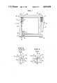
- FIG. 1is top view, partially stylized, of a single TFT device embodying the invention
- FIG. 2is a schematic diagram showing the equivalent impedances of a TFT/LC device of the prior art
- FIG. 3is a schematic diagram showing the equivalent impedances of a TFT/LC device having one embodiment of the invention wherein the gate lines of adjacent rows are assumed to be tied to the same potential as the counter electrode;
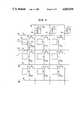
- FIG. 4is a schematic diagram of a portion of a TFT array having an embodiment of the invention and testing circuitry therefore;
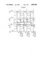
- FIG. 5is a schematic diagram showing an alternate method of testing a TFT array having an embodiment of the invention.
- FIG. 6is another schematic diagram of a TFT array fabricated in accordance with another embodiment of the invention.
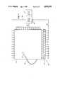
- FIG. 7is a block diagram of a display system having a TFT array, constructed in accordance with the invention, which permits information to be entered into the system in an optical manner.
- TFT 10is formed near an intersection of two metalization lines, or buses, which are disposed in a regular grid-like fashion upon the surface of an insulating substrate (not shown), the lines being electrically insulated one from another in a conventional manner.
- These metalization linesare column lines 12 and 14 and row lines 16 and 18.
- the column and row metalization linesare disposed in a regular grid, with the TFT 10 being disposed within a region defined by pairs of intersecting column and row metalization lines.
- Each of the row metalization lines, such as line 16is fabricated such that it has a plurality of depending spurs, each such spur defining a region which forms a gate electrode 20.
- an active area 22Disposed above and conductively coupled to the gate electrode 20 and a portion of the column metalization line 12 is an active area 22 which is comprised of semiconductor material such as amorphous silicon. This active area is deposited by conventional thin film deposition techniques, such as by vapor phase deposition, sputtering, plasma enhanced chemical vapor phase deposition, or by any similar well known process. Active area 22 may also be seen to overlie a portion of a pel electrode 24, the pel electrode 24 also being formed as a thin film conductive layer upon the substrate. Each pel electrode may be from 10 to 20 mils on a side, although the actual dimension is not critical to the operation of the invention.
- the point of contact between the active area 22 and the column line 12may be considered to be the source electrode of the device.
- the gate electrodeis the aforementioned electrode 20 and the drain electrode is the pel electrode 24.
- Associated with each active area 22is a characteristic length (L) and width (W).
- TFT 10Although one TFT 10 is shown in FIG. 1, it should be realized that a typical TFT array may be comprised of a large number of such devices, such as ten thousand or even a million of such devices disposed in a two dimensional array having many hundreds of row and column lines. Access to a particular one of the TFT 10 devices within the array is gained by energizing a specific combination of column and row metalization lines such that the TFT 10 device which lies at the intersection of the energized lines, such as for example the metalization lines 12 and 16, will be energized. A portion of an adjacent TFT device can be seen to have an active area 28 and a pel electrode 30. Such a TFT device as shown in Fi9.
- the pel electrode 24is essentially a "floating" electrode, or terminal, of the device.
- a typical flat panel display devicewhich includes such an array will have an overlying transparent plate, such as a glass plate, (not shown) disposed in a spaced apart manner from the underlying TFT array.
- the surface of the plate facing the TFTswill have a transparent conductive coating, such as indium tin oxide, deposited thereon to form a counter electrode.
- the region between the TFT array and the counter electrodeis filled with a suitable material, typically a liquid crystal material. Other materials may also be used to provide the optical contrast needed for a display.
- One such materialmay be an el ectrophoretic material.
- an electroluminescent materialcan be used with a modification to the manner in which the counter electrode is provided, as is well known. Circuit continuity to the pel electrode is established through the intervening liquid crystal material to the counter electrode disposed upon the overlying surface of the transparent panel. When suitably energized, the resulting field due to the current flow from the pel electrode through the liquid crystal material into the counter electrode results in a rearrangement of the liquid crystal molecules, thereby providing a visible optical effect, such as a change in optical contrast. Thus, there is created a visible region, or pixel, upon the flat panel display.
- the TFT 10is provided with a conductive strip 26 which connects the pel electrode 24 to an adjacent metalization line, such as the row line 18.
- Strip 26may be comprised of an area of metalization deposited in strip form such that it contacts both the pel electrode 24 metalization and the adjacent row 18 metalization.
- strip 26is comprised of amorphous silicon, which material is the preferred material for fabrication of the active area 22 of TFT device 10.
- the strip 26is comprised of amorphous silicon it is possible to vary the conductivity of the strip 26 by varying the intensity of a source of illumination incident upon the strip 26, due to the fact that amorphous silicon has the property of being an efficient photoconductor.
- the conductivity of amorphous siliconmay be varied over a range of six orders of magnitude from a dark, high resistance state to a fully illuminated, highly conductive state.
- a typical TFT 32 of the prior artis comprised of a source electrode 34, a gate electrode 36, and a drain electrode 38.
- the drain electrode 38is similar to the pel electrode 24 of FIG. 1.
- This loadmay be characterized as having a characteristic impedance comprised of a capacitive element C LC and a resistive component R LC , the subscript referring to the liquid crystal (LC) material.
- a TFT 42in accordance with the invention, also has a source electrode 44, a gate electrode 46, and a drain electrode 48.
- the characteristic impedance 50 experienced by the drain, or pel electrode, 48may be characterized as having three components.
- resistive component R Sassociated with the amorphous silicon strip 26.
- R Sis in parallel with R LC it can be seen that if the resistance associated with R S is much greater than the resistance associated with the liquid crystal material R LC , then the effective resistance experienced by the pel electrode will be essentially that of R LC . Only during the testing of the array, due to high illumination of the strip 26, is the resistance of the strip a factor. During testing of the array, in accordance with the invention, the components C LC and R LC are not present due to the fact that there is no liquid crystal material adjacent to the pel electrode. Thus, the pel electrode 24 experiences only the resistance R S associated with the strip 26.
- the strip 26has a length L S and a width W S .
- a typical width of strip 26may be one half of a mil.
- the resistance of such a strip of amorphous siliconis proportional to a ratio of the length to the width of the strip.
- the ratio of the resistance Rs (Ls/Ws>1) of the strip to the off resistance of the TFT (L/W ⁇ 1)may be adjusted such that a ratio of ten, one hundred, or even more may be obtained.
- R Shas a minimal effect during normal device operation, which operation may include illumination from a backlight.
- the contacts to the amorphous silicon strip 26will not be ohmic.
- the pel electrode 24 voltageis small and the barrier contacts to the strip 26 will add to the strip impedance R S .
- the barrier contactswill break down and this, together with high illumination, will significantly lower the strip impedance.
- the source of illuminationmay be varied to vary the conductivity of the strip 26 to simulate a typical liquid crystal load.
- the value of R Smay be made much smaller than the characteristic liquid crystal load thereby enabling the TFT characteristics themselves to be readily measured.
- each of the TFT deviceshas an associated resistance connecting the pel electrode of each to an adjacent row line.
- TFT device T 11may be seen to have a pel electrode 66 which is connected via a resistor R S11 to adjacent row lines 54, which row line 54 is used during the normal operation of the display to access the TFT devices T 21 , T 22 , T 23 , etc.
- This resistance R S11is representative of the characteristic resistance of the strip 26 of FIG. 1.
- a beam 68 of radiationis focused to a spot 70 upon the strip 26.
- a suitable source of focused radiationmay be a laser (not shown) or some other source of radiation which may be focused to a spot having a sufficient intensity to cause the strip 26 to become conductive.
- the focused beamwould be rapidly scanned in raster fashion over the entire array, thereby testing in sequence each TFT.
- a positive gate potential V Gis applied to the associated row line 52 and a source of positive drain potential V D is applied to the adjacent row line 54 associated with T 21 .
- a typical range of values for V Gmay be from zero to 20 volts and a typical range of values for V D may be from zero to 20 volts. Due to the potentials V G and V D current is caused to flow through the resistance R S11 and through the TFT device T 11 .
- a current sensing meansis provided at the output of column line 60 in order to provide a complete circuit path for the current i s .
- Such a current sensing meanssuch as an operational amplifier 70 having a feedback resistance R F , operates as a current to voltage converter and develops a voltage output V out which is proportional to the magnitude of the current i S while maintaining the potential of line 60 at a ground potential.
- one TFT deviceis tested at a time due to the radiation being focused to a spot which illuminates a single strip 26.
- the focused beam of radiation 68is moved from TFT device to TFT device to test each in sequence. As can be seen all of the TFT devices within a row may be tested in this manner by shifting the beam of radiation 68 in a direction from left to right in the drawing of FIG. 4.
- the voltage V Gwould be applied to row line 54 and the voltage v D would be applied to row line 56 in order to test this row of devices.
- a row line associated with a row of TFT devices which is not being testedis grounded to prevent current from other TFT devices from possibly interfering with the measurement of the selected TFT.
- FIG. 5there is shown an alternate method, in accordance with the invention, of testing an array of TFT devices.
- a plurality of row lines 76 thru 82 and column lines 84 thru 88are provided for connecting to a plurality of TFT devices labeled T 11 , T 12 , T 13 , etc.
- a plurality of operational amplifiers 90, 92 and 94are provided each having one input terminal connected to a respective column line.
- a beam of incident radiation 96is shown to be focused in the shape of a bar 98.
- Bar 98illuminates a plurality of the amorphous silicon strips 26, shown in FIG. 5 by their characteristic resistances R 21 , R 22 and R 23 .
- V G and V Dare applied to the associated and adjacent row lines, respectively, in order to generate a flow of current through each of the TFT devices within the row.
- a plurality of TFT devices within a rowmay thereby be simultaneously energized and tested.
- the resulting currents, shown as i 21 , i 22 and i 23flow into the virtual ground presented by a noninverting terminal of each of a respective one of the operational amplifiers 90 thru 94.
- Amplifiers 90 thru 94are provided, as in FIG. 4, with a feedback resistance R F in a well known inverting amplifier configuration.
- Each of the operational amplifierswill thereby have a voltage output shown as, for example, V out1 .
- Each of these resulting output voltagesmay be individually measured by suitable measuring equipment (not shown) or a plurality of such voltage outputs may be coupled to a suitable multiplexing device such that each voltage may be applied in sequence to a common voltage measuring device.
- Each of the TFT measuring methods and apparatus as shown in FIGS. 4 and 5may be utilized to characterize a number of electrical parameters associated with the TFT devices within an array.
- the parameters which may be desired to be characterizedmay be the on-resistance of the device, the off-resistance of the device, and a number of other well known parameters.
- the threshold voltage of a TFT devicemay be determined by maintaining V D and the illumination intensity at a fixed level while varying the magnitude of V G while simultaneously measuring the output voltage of the respective operational amplifier.
- the conductive strip 26 having an associated resistance R S32forms an electrical connection between a pel electrode 100 and an adjacent column line 62.
- the three terminals of the TFT device under testnamely T 32
- T 32the three terminals of the TFT device under test
- the three terminals of the TFT device under testare accessed through the associated row line 56, the associated column line 60 and the adjacent column line 62.
- this configurationmay be simpler to fabricate.
- a testing sequence for this type of arrangementwould be limited to testing one TFT device at a time due to the fact that multiple devices under test cannot each contribute a current to a common column line. This may not, however, be a significant limitation in that all of the rows and columns may be simultaneously contacted.
- Voltages V G and V Dmay then be rapidly switched from one TFT device to another, via electronic means such as switches 71 and 73, much as is done in the typical row-at-a-time scanning of the display panel during the normal operation of such a panel.
- the focused illumination 70may be rapidly scanned across the array.
- the conductive strip 26may be comprised of a thin film of a metal, such as aluminum. During the testing phase such a metallic strip would provide the pel electrode contact material. Other conductive materials are also possible. After testing, the metallic strip would be required to be removed from the TFT device by, possibly, laser burnout deletion or by some other process. A batch process which involved etching away the metallic strips 26 may also be employed to facilitate the simultaneous removal of the strips. It can be appreciated, however, that if the material utilized for the conductive strip 26 is amorphous silicon that no additional materials or processing would be required during the fabrication of the array.
- Each conductive strip 26would be deposited upon the substrate at the same time that the TFT devices are deposited since each would be comprised of the same amorphous silicon material. Also, amorphous silicon strips do not require physical removal after testing. Inasmuch as they are coupled in parallel with the normal pel electrode load, their intrinsically high resistance when not illuminated would effectively remove them from the circuit.
- amorphous silicon stripsresults in other utilities for the method and apparatus of the invention, beyond those disclosed above relating to the testing of an array of the TFT devices.
- a light penin this case a light-emitting pen
- draw lines on the display or to point to items on the screen
- an external light and a transparencyto create an image on the display.
- the displaywould be equipped with current sensing circuitry, such as in FIG. 5 for example.
- the arraywould be scanned electronically row by row and a sensed current would correspond to those TFTs (pixel elements) that had been illuminated.
- the sensed datawould be written line by line into a display frame buffer associated with the display in order to form an image corresponding to the illuminated portion of the screen.
- FIG. 7one such optical writing system 101 is shown to be comprised of a display panel 102 having a TFT/LC array constructed, in accordance with the invention, with amorphous silicon strips connecting each pel electrode to an adjacent metalization line.
- a display controller 104has a plurality of column outputs 106 and a plurality of row outputs 108 for sequentially energizing specific pixels (not shown) of the panel 102 in accordance with the contents of a display buffer 110.
- Buffer 110is typically a memory device which stores data expressive of the image, such as textual and/or graphical images, displayed upon the panel 102.
- Controller 104may be a dedicated controller or may be embedded within a data processing system, such as a word processing or some other type of system.
- a light source meanssuch as a light emitting pen 112 for illuminating desired portions of the panel 102 with a light output 113.
- a plurality of current sense means 114are also coupled to panel 102 .
- Each of the current sense means 114may be an operational amplifier having a suitable feedback resistor R F and an input terminal coupled to a column line of the panel, much as is shown in FIG. 5.
- the output of each current sense means 114is coupled by output lines 116 to the display controller 104.
- controller 104activates a particular one of the row lines 108 and subsequently activates the column lines 106 in order to interrogate one row of the display. This procedure is repeated for each row until the entire display has been interrogated, at which time the process is repeated. If, during the activation of a particular row and column, a signal is received from the corresponding current sense means 114, the controller 104 determines which portion of the display is being illuminated by pen 112.
- controller 104it is possible to directly input information to the display controller 104 by illuminating a desired pixel or pixels, thereby reducing the normally high resistance of the strips associated with the underlying TFT devices to cause a current flow through these devices.
- This informationmay be utilized to cause controller 104 to perform some action, such as to select a specific item from a displayed menu of items.
- This informationmay also be stored within buffer 110 by controller 104 for subsequent display upon the panel 102.
Landscapes
- Physics & Mathematics (AREA)
- Engineering & Computer Science (AREA)
- General Physics & Mathematics (AREA)
- Nonlinear Science (AREA)
- Microelectronics & Electronic Packaging (AREA)
- Manufacturing & Machinery (AREA)
- Computer Hardware Design (AREA)
- Chemical & Material Sciences (AREA)
- Crystallography & Structural Chemistry (AREA)
- Optics & Photonics (AREA)
- Power Engineering (AREA)
- Theoretical Computer Science (AREA)
- Mathematical Physics (AREA)
- Health & Medical Sciences (AREA)
- Condensed Matter Physics & Semiconductors (AREA)
- Electromagnetism (AREA)
- Toxicology (AREA)
- Liquid Crystal (AREA)
- Thin Film Transistor (AREA)
- Liquid Crystal Display Device Control (AREA)
- Testing Or Measuring Of Semiconductors Or The Like (AREA)
Abstract
Description
Claims (8)
Priority Applications (4)
| Application Number | Priority Date | Filing Date | Title |
|---|---|---|---|
| US06/945,935US4819038A (en) | 1986-12-22 | 1986-12-22 | TFT array for liquid crystal displays allowing in-process testing |
| JP62282290AJP2559773B2 (en) | 1986-12-22 | 1987-11-10 | Thin film transistor array device |
| EP87117757AEP0272506B1 (en) | 1986-12-22 | 1987-12-01 | Thin film transistor array for liquid crystal displays allowing in-process testing, testing method, and information entry system comprising such an array |
| DE3751111TDE3751111T2 (en) | 1986-12-22 | 1987-12-01 | Thin film transistor matrix for liquid crystal display with test possibility during manufacture, test method and arrangement for information input with such a matrix. |
Applications Claiming Priority (1)
| Application Number | Priority Date | Filing Date | Title |
|---|---|---|---|
| US06/945,935US4819038A (en) | 1986-12-22 | 1986-12-22 | TFT array for liquid crystal displays allowing in-process testing |
Publications (1)
| Publication Number | Publication Date |
|---|---|
| US4819038Atrue US4819038A (en) | 1989-04-04 |
Family
ID=25483731
Family Applications (1)
| Application Number | Title | Priority Date | Filing Date |
|---|---|---|---|
| US06/945,935Expired - LifetimeUS4819038A (en) | 1986-12-22 | 1986-12-22 | TFT array for liquid crystal displays allowing in-process testing |
Country Status (4)
| Country | Link |
|---|---|
| US (1) | US4819038A (en) |
| EP (1) | EP0272506B1 (en) |
| JP (1) | JP2559773B2 (en) |
| DE (1) | DE3751111T2 (en) |
Cited By (55)
| Publication number | Priority date | Publication date | Assignee | Title |
|---|---|---|---|---|
| US4965565A (en)* | 1987-05-06 | 1990-10-23 | Nec Corporation | Liquid crystal display panel having a thin-film transistor array for displaying a high quality picture |
| US5057775A (en)* | 1990-05-04 | 1991-10-15 | Genrad, Inc. | Method of testing control matrices for flat-panel displays |
| US5075237A (en)* | 1990-07-26 | 1991-12-24 | Industrial Technology Research Institute | Process of making a high photosensitive depletion-gate thin film transistor |
| US5077596A (en)* | 1990-02-01 | 1991-12-31 | Mitsubishi Denki Kabushiki Kaisha | Semiconductor device |
| WO1992009900A1 (en)* | 1990-11-26 | 1992-06-11 | Photon Dynamics, Inc. | Method and apparatus for testing lcd panel array |
| US5175504A (en)* | 1991-06-17 | 1992-12-29 | Photon Dynamics, Inc. | Method and apparatus for automatically inspecting and repairing a simple matrix circuit panel |
| US5179345A (en)* | 1989-12-13 | 1993-01-12 | International Business Machines Corporation | Method and apparatus for analog testing |
| US5184082A (en)* | 1991-09-18 | 1993-02-02 | Honeywell Inc. | Apparatus and method for testing an active matrix pixel display |
| US5196911A (en)* | 1990-07-26 | 1993-03-23 | Industrial Technology Research Institute | High photosensitive depletion-gate thin film transistor |
| US5204617A (en)* | 1990-10-22 | 1993-04-20 | Ezel, Inc. | Liquid crystal panel inspection method |
| US5206749A (en)* | 1990-12-31 | 1993-04-27 | Kopin Corporation | Liquid crystal display having essentially single crystal transistors pixels and driving circuits |
| US5235272A (en)* | 1991-06-17 | 1993-08-10 | Photon Dynamics, Inc. | Method and apparatus for automatically inspecting and repairing an active matrix LCD panel |
| US5258320A (en)* | 1990-12-31 | 1993-11-02 | Kopin Corporation | Single crystal silicon arrayed devices for display panels |
| US5268569A (en)* | 1992-07-22 | 1993-12-07 | Minnesota Mining And Manufacturing Company | Imaging system having optimized electrode geometry and processing |
| US5332893A (en)* | 1992-07-22 | 1994-07-26 | Minnesota Mining And Manufacturing Company | Imaging system and device having a simplified electrode design |
| US5362671A (en)* | 1990-12-31 | 1994-11-08 | Kopin Corporation | Method of fabricating single crystal silicon arrayed devices for display panels |
| US5432461A (en)* | 1991-06-28 | 1995-07-11 | Photon Dynamics, Inc. | Method of testing active matrix liquid crystal display substrates |
| US5444385A (en)* | 1991-09-10 | 1995-08-22 | Photon Dynamics, Inc. | Testing apparatus for liquid crystal display substrates |
| US5459409A (en)* | 1991-09-10 | 1995-10-17 | Photon Dynamics, Inc. | Testing device for liquid crystal display base plate |
| US5465052A (en)* | 1991-09-10 | 1995-11-07 | Photon Dynamics, Inc. | Method of testing liquid crystal display substrates |
| US5504438A (en)* | 1991-09-10 | 1996-04-02 | Photon Dynamics, Inc. | Testing method for imaging defects in a liquid crystal display substrate |
| US5528397A (en)* | 1991-12-03 | 1996-06-18 | Kopin Corporation | Single crystal silicon transistors for display panels |
| US5543729A (en)* | 1991-09-10 | 1996-08-06 | Photon Dynamics, Inc. | Testing apparatus and connector for liquid crystal display substrates |
| US5546013A (en)* | 1993-03-05 | 1996-08-13 | International Business Machines Corporation | Array tester for determining contact quality and line integrity in a TFT/LCD |
| US5550484A (en)* | 1994-10-12 | 1996-08-27 | Frontec Incorporated | Apparatus and method for inspecting thin film transistor |
| US5744967A (en)* | 1995-08-24 | 1998-04-28 | Sorensen; Brent A. | Apparatus for detecting intermittent and continuous faults in multiple conductor wiring and terminations for electronic systems |
| US5949194A (en)* | 1996-05-16 | 1999-09-07 | Fuji Electric Co., Ltd. | Display element drive method |
| US5952674A (en)* | 1998-03-18 | 1999-09-14 | International Business Machines Corporation | Topography monitor |
| USRE37847E1 (en) | 1990-11-30 | 2002-09-17 | Photon Dynamics, Inc. | Method and apparatus for testing LCD panel array prior to shorting bar removal |
| US6545500B1 (en) | 1999-12-08 | 2003-04-08 | John E. Field | Use of localized temperature change in determining the location and character of defects in flat-panel displays |
| US20040013019A1 (en)* | 2002-07-19 | 2004-01-22 | Nec Corporation | Semiconductor, image output device, and driving method of a functional device |
| US6697037B1 (en) | 1996-04-29 | 2004-02-24 | International Business Machines Corporation | TFT LCD active data line repair |
| US20050104615A1 (en)* | 2003-11-13 | 2005-05-19 | Dong-Guk Kim | Apparatus for testing liquid crystal display device and testing method thereof |
| US20050174139A1 (en)* | 2003-10-14 | 2005-08-11 | Mahendran Chidambaram | Apparatus for high speed probing of flat panel displays |
| US20050179453A1 (en)* | 2004-02-12 | 2005-08-18 | Shinichi Kurita | Integrated substrate transfer module |
| US20050179451A1 (en)* | 2004-02-12 | 2005-08-18 | Applied Materials, Inc. | Configurable prober for TFT LCD array testing |
| US20050179452A1 (en)* | 2004-02-12 | 2005-08-18 | Applied Materials, Inc. | Configurable prober for TFT LCD array test |
| US20050270059A1 (en)* | 2004-05-31 | 2005-12-08 | Naoki Ando | Display apparatus and inspection method |
| US20060022694A1 (en)* | 2004-07-29 | 2006-02-02 | Applied Materials, Inc. | Large substrate test system |
| US20060028230A1 (en)* | 2004-08-03 | 2006-02-09 | Applied Materials, Inc. | Method for testing pixels for LCD TFT displays |
| US20060038554A1 (en)* | 2004-02-12 | 2006-02-23 | Applied Materials, Inc. | Electron beam test system stage |
| US20060244467A1 (en)* | 2005-04-29 | 2006-11-02 | Applied Materials, Inc. | In-line electron beam test system |
| US20060273815A1 (en)* | 2005-06-06 | 2006-12-07 | Applied Materials, Inc. | Substrate support with integrated prober drive |
| US20070164769A1 (en)* | 2006-01-17 | 2007-07-19 | Gebara Fadi H | Active cancellation matrix for process parameter measurements |
| CN100336099C (en)* | 2003-09-10 | 2007-09-05 | 友达光电股份有限公司 | Display panel with circuit connection test design |
| US20070216428A1 (en)* | 2006-03-14 | 2007-09-20 | Ralf Schmid | Method to reduce cross talk in a multi column e-beam test system |
| US20070296426A1 (en)* | 2006-05-31 | 2007-12-27 | Applied Materials, Inc. | Prober for electronic device testing on large area substrates |
| US20070296437A1 (en)* | 2006-05-31 | 2007-12-27 | Johnston Benjamin M | Mini-prober for tft-lcd testing |
| US20080117144A1 (en)* | 2002-05-21 | 2008-05-22 | Daiju Nakano | Inspection device and inspection method for active matrix panel, and manufacturing method for active matrix organic light emitting diode panel |
| US20080251019A1 (en)* | 2007-04-12 | 2008-10-16 | Sriram Krishnaswami | System and method for transferring a substrate into and out of a reduced volume chamber accommodating multiple substrates |
| US20090122056A1 (en)* | 2002-06-19 | 2009-05-14 | Akt Electron Beam Technology Gmbh | Drive apparatus with improved testing properties |
| CN101107534B (en)* | 2005-05-02 | 2012-04-25 | 株式会社岛津制作所 | TFT array substrate inspecting apparatus |
| US20130265066A1 (en)* | 2012-04-06 | 2013-10-10 | Industrial Technology Research Institute | Pixel array module with self-test function and method thereof |
| US9865517B2 (en)* | 2015-12-31 | 2018-01-09 | Boe Technology Group Co., Ltd. | Test element group, array substrate, test device and test method |
| CN116360168A (en)* | 2023-05-11 | 2023-06-30 | 惠科股份有限公司 | display device |
Families Citing this family (9)
| Publication number | Priority date | Publication date | Assignee | Title |
|---|---|---|---|---|
| JPH04351972A (en)* | 1990-04-26 | 1992-12-07 | Genrad Inc | Testing method of control matrix for flat panel display |
| JPH06110069A (en)* | 1992-09-29 | 1994-04-22 | Matsushita Electric Ind Co Ltd | Electronic component defect repairing method and defect repairing apparatus |
| JPH07509105A (en)* | 1993-05-13 | 1995-10-05 | プロエンサ・アウグスト、カルロス・ホルヘ・ラミロ | VLSI-quality crystal semiconductor substrate supply method |
| JP3107039B2 (en)* | 1998-03-20 | 2000-11-06 | 日本電気株式会社 | Surface light source prober device and inspection method |
| JP2004264349A (en)* | 2003-02-07 | 2004-09-24 | Agilent Technol Inc | Active matrix display circuit board, display panel including the same, inspection method therefor, and inspection apparatus therefor |
| JP5305730B2 (en) | 2008-05-12 | 2013-10-02 | キヤノン株式会社 | Semiconductor device manufacturing method and manufacturing apparatus thereof |
| WO2010143336A1 (en)* | 2009-06-09 | 2010-12-16 | シャープ株式会社 | Electronic device |
| CN104166026A (en)* | 2014-08-29 | 2014-11-26 | 苏州市吴中区胥口广博模具加工厂 | Small display screen lightening test bench |
| CN104637426B (en)* | 2015-03-04 | 2017-04-05 | 京东方科技集团股份有限公司 | Load testing circuit, method and display device |
Citations (2)
| Publication number | Priority date | Publication date | Assignee | Title |
|---|---|---|---|---|
| US3930304A (en)* | 1972-11-18 | 1976-01-06 | Robert Bosch G.M.B.H. | Method and apparatus for selective burnout trimming of integrated circuit units |
| EP0163956A2 (en)* | 1984-05-04 | 1985-12-11 | Energy Conversion Devices, Inc. | Intergrated radiation sensing array |
Family Cites Families (5)
| Publication number | Priority date | Publication date | Assignee | Title |
|---|---|---|---|---|
| US3801910A (en)* | 1972-07-03 | 1974-04-02 | Ibm | Externally accessing mechanical difficult to access circuit nodes using photo-responsive conductors in integrated circuits |
| US3849872A (en)* | 1972-10-24 | 1974-11-26 | Ibm | Contacting integrated circuit chip terminal through the wafer kerf |
| JPS58140781A (en)* | 1982-02-17 | 1983-08-20 | 株式会社日立製作所 | image display device |
| JPS59201441A (en)* | 1983-04-30 | 1984-11-15 | Toshiba Corp | Fuse cutting method utilizing converged ion beam |
| JPS61170724A (en)* | 1985-01-25 | 1986-08-01 | Seiko Instr & Electronics Ltd | Substrate for active matrix display device |
- 1986
- 1986-12-22USUS06/945,935patent/US4819038A/ennot_activeExpired - Lifetime
- 1987
- 1987-11-10JPJP62282290Apatent/JP2559773B2/ennot_activeExpired - Lifetime
- 1987-12-01DEDE3751111Tpatent/DE3751111T2/ennot_activeExpired - Lifetime
- 1987-12-01EPEP87117757Apatent/EP0272506B1/ennot_activeExpired - Lifetime
Patent Citations (2)
| Publication number | Priority date | Publication date | Assignee | Title |
|---|---|---|---|---|
| US3930304A (en)* | 1972-11-18 | 1976-01-06 | Robert Bosch G.M.B.H. | Method and apparatus for selective burnout trimming of integrated circuit units |
| EP0163956A2 (en)* | 1984-05-04 | 1985-12-11 | Energy Conversion Devices, Inc. | Intergrated radiation sensing array |
Cited By (89)
| Publication number | Priority date | Publication date | Assignee | Title |
|---|---|---|---|---|
| US4965565A (en)* | 1987-05-06 | 1990-10-23 | Nec Corporation | Liquid crystal display panel having a thin-film transistor array for displaying a high quality picture |
| US5561381A (en)* | 1989-12-13 | 1996-10-01 | International Business Machines Corporation | Method for testing a partially constructed electronic circuit |
| US5179345A (en)* | 1989-12-13 | 1993-01-12 | International Business Machines Corporation | Method and apparatus for analog testing |
| US5077596A (en)* | 1990-02-01 | 1991-12-31 | Mitsubishi Denki Kabushiki Kaisha | Semiconductor device |
| US5057775A (en)* | 1990-05-04 | 1991-10-15 | Genrad, Inc. | Method of testing control matrices for flat-panel displays |
| US5075237A (en)* | 1990-07-26 | 1991-12-24 | Industrial Technology Research Institute | Process of making a high photosensitive depletion-gate thin film transistor |
| US5196911A (en)* | 1990-07-26 | 1993-03-23 | Industrial Technology Research Institute | High photosensitive depletion-gate thin film transistor |
| US5204617A (en)* | 1990-10-22 | 1993-04-20 | Ezel, Inc. | Liquid crystal panel inspection method |
| WO1992009900A1 (en)* | 1990-11-26 | 1992-06-11 | Photon Dynamics, Inc. | Method and apparatus for testing lcd panel array |
| US5363037A (en)* | 1990-11-26 | 1994-11-08 | Photon Dynamics, Inc. | Method and apparatus for testing LCD panel array |
| US5285150A (en)* | 1990-11-26 | 1994-02-08 | Photon Dynamics, Inc. | Method and apparatus for testing LCD panel array |
| USRE37847E1 (en) | 1990-11-30 | 2002-09-17 | Photon Dynamics, Inc. | Method and apparatus for testing LCD panel array prior to shorting bar removal |
| US5258320A (en)* | 1990-12-31 | 1993-11-02 | Kopin Corporation | Single crystal silicon arrayed devices for display panels |
| US6414783B2 (en) | 1990-12-31 | 2002-07-02 | Kopin Corporation | Method of transferring semiconductors |
| US5206749A (en)* | 1990-12-31 | 1993-04-27 | Kopin Corporation | Liquid crystal display having essentially single crystal transistors pixels and driving circuits |
| US6232136B1 (en) | 1990-12-31 | 2001-05-15 | Kopin Corporation | Method of transferring semiconductors |
| US5362671A (en)* | 1990-12-31 | 1994-11-08 | Kopin Corporation | Method of fabricating single crystal silicon arrayed devices for display panels |
| US5175504A (en)* | 1991-06-17 | 1992-12-29 | Photon Dynamics, Inc. | Method and apparatus for automatically inspecting and repairing a simple matrix circuit panel |
| US5235272A (en)* | 1991-06-17 | 1993-08-10 | Photon Dynamics, Inc. | Method and apparatus for automatically inspecting and repairing an active matrix LCD panel |
| US5459410A (en)* | 1991-06-17 | 1995-10-17 | Photon Dynamics, Inc. | Method and apparatus for automatically inspecting and repairing an active matrix LCD panel |
| US5432461A (en)* | 1991-06-28 | 1995-07-11 | Photon Dynamics, Inc. | Method of testing active matrix liquid crystal display substrates |
| US5444385A (en)* | 1991-09-10 | 1995-08-22 | Photon Dynamics, Inc. | Testing apparatus for liquid crystal display substrates |
| US5465052A (en)* | 1991-09-10 | 1995-11-07 | Photon Dynamics, Inc. | Method of testing liquid crystal display substrates |
| US5504438A (en)* | 1991-09-10 | 1996-04-02 | Photon Dynamics, Inc. | Testing method for imaging defects in a liquid crystal display substrate |
| US5459409A (en)* | 1991-09-10 | 1995-10-17 | Photon Dynamics, Inc. | Testing device for liquid crystal display base plate |
| US5543729A (en)* | 1991-09-10 | 1996-08-06 | Photon Dynamics, Inc. | Testing apparatus and connector for liquid crystal display substrates |
| US5184082A (en)* | 1991-09-18 | 1993-02-02 | Honeywell Inc. | Apparatus and method for testing an active matrix pixel display |
| US5528397A (en)* | 1991-12-03 | 1996-06-18 | Kopin Corporation | Single crystal silicon transistors for display panels |
| US5332893A (en)* | 1992-07-22 | 1994-07-26 | Minnesota Mining And Manufacturing Company | Imaging system and device having a simplified electrode design |
| US5268569A (en)* | 1992-07-22 | 1993-12-07 | Minnesota Mining And Manufacturing Company | Imaging system having optimized electrode geometry and processing |
| US5546013A (en)* | 1993-03-05 | 1996-08-13 | International Business Machines Corporation | Array tester for determining contact quality and line integrity in a TFT/LCD |
| US5550484A (en)* | 1994-10-12 | 1996-08-27 | Frontec Incorporated | Apparatus and method for inspecting thin film transistor |
| US5744967A (en)* | 1995-08-24 | 1998-04-28 | Sorensen; Brent A. | Apparatus for detecting intermittent and continuous faults in multiple conductor wiring and terminations for electronic systems |
| US6697037B1 (en) | 1996-04-29 | 2004-02-24 | International Business Machines Corporation | TFT LCD active data line repair |
| US5949194A (en)* | 1996-05-16 | 1999-09-07 | Fuji Electric Co., Ltd. | Display element drive method |
| US5952674A (en)* | 1998-03-18 | 1999-09-14 | International Business Machines Corporation | Topography monitor |
| US6545500B1 (en) | 1999-12-08 | 2003-04-08 | John E. Field | Use of localized temperature change in determining the location and character of defects in flat-panel displays |
| US20080117144A1 (en)* | 2002-05-21 | 2008-05-22 | Daiju Nakano | Inspection device and inspection method for active matrix panel, and manufacturing method for active matrix organic light emitting diode panel |
| US8208114B2 (en) | 2002-06-19 | 2012-06-26 | Akt Electron Beam Technology Gmbh | Drive apparatus with improved testing properties |
| US20090122056A1 (en)* | 2002-06-19 | 2009-05-14 | Akt Electron Beam Technology Gmbh | Drive apparatus with improved testing properties |
| US20040013019A1 (en)* | 2002-07-19 | 2004-01-22 | Nec Corporation | Semiconductor, image output device, and driving method of a functional device |
| US7665816B2 (en) | 2002-07-19 | 2010-02-23 | Nec Corporation | Image output device with an injector |
| US7012849B2 (en)* | 2002-07-19 | 2006-03-14 | Nec Corporation | Semiconductor, image output device, and driving method of a functional device |
| US20060119634A1 (en)* | 2002-07-19 | 2006-06-08 | Nec Corporation | Image output device with an injector |
| US8228269B2 (en)* | 2003-05-21 | 2012-07-24 | International Business Machines Corporation | Inspection device and inspection method for active matrix panel, and manufacturing method for active matrix organic light emitting diode panel |
| CN100336099C (en)* | 2003-09-10 | 2007-09-05 | 友达光电股份有限公司 | Display panel with circuit connection test design |
| US20050174139A1 (en)* | 2003-10-14 | 2005-08-11 | Mahendran Chidambaram | Apparatus for high speed probing of flat panel displays |
| US7477369B2 (en)* | 2003-11-13 | 2009-01-13 | Lg Display Co., Ltd. | Apparatus for testing liquid crystal display device and testing method thereof |
| US20050104615A1 (en)* | 2003-11-13 | 2005-05-19 | Dong-Guk Kim | Apparatus for testing liquid crystal display device and testing method thereof |
| US20080111577A1 (en)* | 2004-02-12 | 2008-05-15 | Shinichi Kurita | Integrated Substrate Transfer Module |
| US7319335B2 (en) | 2004-02-12 | 2008-01-15 | Applied Materials, Inc. | Configurable prober for TFT LCD array testing |
| US7919972B2 (en) | 2004-02-12 | 2011-04-05 | Applied Materials, Inc. | Integrated substrate transfer module |
| US20050179452A1 (en)* | 2004-02-12 | 2005-08-18 | Applied Materials, Inc. | Configurable prober for TFT LCD array test |
| US7847566B2 (en) | 2004-02-12 | 2010-12-07 | Applied Materials, Inc. | Configurable prober for TFT LCD array test |
| US20050179451A1 (en)* | 2004-02-12 | 2005-08-18 | Applied Materials, Inc. | Configurable prober for TFT LCD array testing |
| US20060038554A1 (en)* | 2004-02-12 | 2006-02-23 | Applied Materials, Inc. | Electron beam test system stage |
| US7355418B2 (en) | 2004-02-12 | 2008-04-08 | Applied Materials, Inc. | Configurable prober for TFT LCD array test |
| US20080061807A1 (en)* | 2004-02-12 | 2008-03-13 | Matthias Brunner | Configurable Prober for TFT LCD Array Test |
| US20050179453A1 (en)* | 2004-02-12 | 2005-08-18 | Shinichi Kurita | Integrated substrate transfer module |
| US7330021B2 (en) | 2004-02-12 | 2008-02-12 | Applied Materials, Inc. | Integrated substrate transfer module |
| US20050270059A1 (en)* | 2004-05-31 | 2005-12-08 | Naoki Ando | Display apparatus and inspection method |
| US7358757B2 (en) | 2004-05-31 | 2008-04-15 | Sony Corporation | Display apparatus and inspection method |
| US20060226866A1 (en)* | 2004-05-31 | 2006-10-12 | Naoki Ando | Display apparatus and inspection method |
| US7145358B2 (en)* | 2004-05-31 | 2006-12-05 | Sony Corporation | Display apparatus and inspection method |
| US20060022694A1 (en)* | 2004-07-29 | 2006-02-02 | Applied Materials, Inc. | Large substrate test system |
| US7075323B2 (en) | 2004-07-29 | 2006-07-11 | Applied Materials, Inc. | Large substrate test system |
| US7256606B2 (en) | 2004-08-03 | 2007-08-14 | Applied Materials, Inc. | Method for testing pixels for LCD TFT displays |
| US20060028230A1 (en)* | 2004-08-03 | 2006-02-09 | Applied Materials, Inc. | Method for testing pixels for LCD TFT displays |
| US7746088B2 (en) | 2005-04-29 | 2010-06-29 | Applied Materials, Inc. | In-line electron beam test system |
| US20060244467A1 (en)* | 2005-04-29 | 2006-11-02 | Applied Materials, Inc. | In-line electron beam test system |
| US20090195262A1 (en)* | 2005-04-29 | 2009-08-06 | Abboud Fayez E | In-line electron beam test system |
| US7535238B2 (en) | 2005-04-29 | 2009-05-19 | Applied Materials, Inc. | In-line electron beam test system |
| CN101107534B (en)* | 2005-05-02 | 2012-04-25 | 株式会社岛津制作所 | TFT array substrate inspecting apparatus |
| US20060273815A1 (en)* | 2005-06-06 | 2006-12-07 | Applied Materials, Inc. | Substrate support with integrated prober drive |
| US20080284461A1 (en)* | 2006-01-17 | 2008-11-20 | Gebara Fadi H | Active cancellation matrix for process parameter measurements |
| US20070164769A1 (en)* | 2006-01-17 | 2007-07-19 | Gebara Fadi H | Active cancellation matrix for process parameter measurements |
| US7394276B2 (en)* | 2006-01-17 | 2008-07-01 | International Business Machines Corporation | Active cancellation matrix for process parameter measurements |
| US7569818B2 (en) | 2006-03-14 | 2009-08-04 | Applied Materials, Inc. | Method to reduce cross talk in a multi column e-beam test system |
| US20070216428A1 (en)* | 2006-03-14 | 2007-09-20 | Ralf Schmid | Method to reduce cross talk in a multi column e-beam test system |
| US20070296437A1 (en)* | 2006-05-31 | 2007-12-27 | Johnston Benjamin M | Mini-prober for tft-lcd testing |
| US7786742B2 (en) | 2006-05-31 | 2010-08-31 | Applied Materials, Inc. | Prober for electronic device testing on large area substrates |
| US7602199B2 (en) | 2006-05-31 | 2009-10-13 | Applied Materials, Inc. | Mini-prober for TFT-LCD testing |
| US20070296426A1 (en)* | 2006-05-31 | 2007-12-27 | Applied Materials, Inc. | Prober for electronic device testing on large area substrates |
| US20080251019A1 (en)* | 2007-04-12 | 2008-10-16 | Sriram Krishnaswami | System and method for transferring a substrate into and out of a reduced volume chamber accommodating multiple substrates |
| US20130265066A1 (en)* | 2012-04-06 | 2013-10-10 | Industrial Technology Research Institute | Pixel array module with self-test function and method thereof |
| US9007078B2 (en)* | 2012-04-06 | 2015-04-14 | Industrial Technology Research Institute | Pixel array module with self-test function and method thereof |
| US9865517B2 (en)* | 2015-12-31 | 2018-01-09 | Boe Technology Group Co., Ltd. | Test element group, array substrate, test device and test method |
| CN116360168A (en)* | 2023-05-11 | 2023-06-30 | 惠科股份有限公司 | display device |
| CN116360168B (en)* | 2023-05-11 | 2023-08-18 | 惠科股份有限公司 | display device |
Also Published As
| Publication number | Publication date |
|---|---|
| EP0272506A3 (en) | 1991-05-29 |
| JPS63167333A (en) | 1988-07-11 |
| DE3751111D1 (en) | 1995-04-06 |
| EP0272506A2 (en) | 1988-06-29 |
| JP2559773B2 (en) | 1996-12-04 |
| EP0272506B1 (en) | 1995-03-01 |
| DE3751111T2 (en) | 1995-09-14 |
Similar Documents
| Publication | Publication Date | Title |
|---|---|---|
| US4819038A (en) | TFT array for liquid crystal displays allowing in-process testing | |
| EP0397244B1 (en) | Touch sensor array systems and display systems incorporating such | |
| US5377030A (en) | Method for testing active matrix liquid crystal by measuring voltage due to charge in a supplemental capacitor | |
| US6172410B1 (en) | Collective substrate of active-matrix substrates, manufacturing method thereof and inspecting method thereof | |
| EP0321073B1 (en) | Liquid crystal display device | |
| TWI471846B (en) | Matrix type liquid crystal display of the active matrix type | |
| US5652632A (en) | LCD apparatus having electrostatic breakdown preventing configuration capable of testing each pixel | |
| US5719648A (en) | Liquid crystal display apparatus and method for producing the same with electrodes for producing a reference signal outside display area | |
| KR100873534B1 (en) | Tft array substrate, tft array testing method, and display unit | |
| US5019001A (en) | Method for manufacturing liquid crystal display device | |
| US10198102B2 (en) | Touch display panel and its controlling method | |
| JPH11142888A (en) | Liquid crystal display device and inspection method thereof | |
| KR970017107A (en) | Array substrate of liquid crystal display device, liquid crystal display device having the array substrate and method of manufacturing array substrate of liquid crystal display device | |
| JPH05240901A (en) | Particle beam system test method for substrate for liquid crystal indicator device | |
| JPH04233619A (en) | Touch sensor array | |
| EP0627722A2 (en) | Light valve device with failure detection circuit | |
| KR0125465B1 (en) | Inspecting method and apparatus for an active matrix substrate | |
| US6677171B1 (en) | Manufacturing method of collective substrate of active-matrix substrates, manufacturing method of active-matrix substrates, and inspecting method of collective substrates of active-matrix substrates | |
| KR101152133B1 (en) | Temperature sensor for display device, thin film transistor array panel including temperature sensor, and liquid crystal display | |
| KR100576629B1 (en) | TFT array board of liquid crystal display and inspection method | |
| JP3316929B2 (en) | Matrix wiring board | |
| JP2516197B2 (en) | Semiconductor element inspection method | |
| JPH0519294A (en) | Line defect correction method for active matrix display device | |
| JPH08262485A (en) | Liquid crystal display device | |
| KR20050006521A (en) | Liquid crystal display and test method thereof |
Legal Events
| Date | Code | Title | Description |
|---|---|---|---|
| AS | Assignment | Owner name:INTERNATIONAL BUSINESS MACHINES CORPORATION, ARMON Free format text:ASSIGNMENT OF ASSIGNORS INTEREST.;ASSIGNOR:ALT, PAUL M.;REEL/FRAME:004652/0127 Effective date:19861222 Owner name:INTERNATIONAL BUSINESS MACHINES CORPORATION, NEW Y Free format text:ASSIGNMENT OF ASSIGNORS INTEREST;ASSIGNOR:ALT, PAUL M.;REEL/FRAME:004652/0127 Effective date:19861222 | |
| STCF | Information on status: patent grant | Free format text:PATENTED CASE | |
| FPAY | Fee payment | Year of fee payment:4 | |
| FPAY | Fee payment | Year of fee payment:8 | |
| FEPP | Fee payment procedure | Free format text:PAYOR NUMBER ASSIGNED (ORIGINAL EVENT CODE: ASPN); ENTITY STATUS OF PATENT OWNER: LARGE ENTITY | |
| FPAY | Fee payment | Year of fee payment:12 | |
| AS | Assignment | Owner name:AU OPTRONICS CORPORATION, TAIWAN Free format text:ASSIGNMENT OF ASSIGNORS INTEREST;ASSIGNOR:INTERNATIONAL BUSINESS MACHINES CORPORATION;REEL/FRAME:016926/0247 Effective date:20051208 |