US4818995A - Parallel transmission system - Google Patents
Parallel transmission systemDownload PDFInfo
- Publication number
- US4818995A US4818995AUS07/051,519US5151987AUS4818995AUS 4818995 AUS4818995 AUS 4818995AUS 5151987 AUS5151987 AUS 5151987AUS 4818995 AUS4818995 AUS 4818995A
- Authority
- US
- United States
- Prior art keywords
- parallel
- mbnb
- line
- blocks
- line codes
- Prior art date
- Legal status (The legal status is an assumption and is not a legal conclusion. Google has not performed a legal analysis and makes no representation as to the accuracy of the status listed.)
- Expired - Fee Related
Links
- 230000005540biological transmissionEffects0.000titleclaimsabstractdescription32
- 238000000034methodMethods0.000claimsdescription9
- 230000008929regenerationEffects0.000description6
- 238000011069regeneration methodMethods0.000description6
- 230000015556catabolic processEffects0.000description3
- 238000006731degradation reactionMethods0.000description3
- 230000001934delayEffects0.000description2
- 238000010586diagramMethods0.000description2
- 230000015654memoryEffects0.000description2
- 230000002411adverseEffects0.000description1
- 230000000694effectsEffects0.000description1
- 238000005070samplingMethods0.000description1
Images


Classifications
- H—ELECTRICITY
- H04—ELECTRIC COMMUNICATION TECHNIQUE
- H04L—TRANSMISSION OF DIGITAL INFORMATION, e.g. TELEGRAPHIC COMMUNICATION
- H04L7/00—Arrangements for synchronising receiver with transmitter
- H04L7/0054—Detection of the synchronisation error by features other than the received signal transition
- H04L7/0066—Detection of the synchronisation error by features other than the received signal transition detection of error based on transmission code rule
- H—ELECTRICITY
- H04—ELECTRIC COMMUNICATION TECHNIQUE
- H04L—TRANSMISSION OF DIGITAL INFORMATION, e.g. TELEGRAPHIC COMMUNICATION
- H04L25/00—Baseband systems
- H04L25/02—Details ; arrangements for supplying electrical power along data transmission lines
- H04L25/14—Channel dividing arrangements, i.e. in which a single bit stream is divided between several baseband channels and reassembled at the receiver
Definitions
- the present inventionrelates to a parallel transmission system for transmitting pulses distributed in parallel.
- bit ratebecomes high, a difference in delay causes a more adverse effect, resulting in a degradation of waveform margin for pulse regeneration, an increase in bit error rates, or the like.
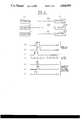
- FIG. 3Such a situation will be described with reference to FIG. 3.
- three pulse trainsare simultaneously transmitted from transmitters 21a to 21c over transmission lines 22a to 22c to receivers 23a to 23c.
- the pulse trainsare received at the receivers 23a to 23c at different times because of the presence of different propagation delays in the transmission lines 22a to 22c, as shown in waveforms (a) to (c) in FIG. 3.
- the received pulsesare sampled by a clock pulse (d) to align them at a smae pulse regeneration time as shown by a dotted-line.
- FIG. 4(a)a signal is converted into a CMI (Coded Mark Inversion) code as shown in FIG. 4(a).
- Coding rule violation(indicated by an arrow in FIG. 4(b)) is applied to each signal at the sending side at the same time.
- the receiving sidedetects this coding rule violation to align or make equal the occurrence times of such violation at each signal by using buffer memories.
- An object of this inventionis to solve the above problems and provide a parallel transmission system which ensures waveform margin for pulse regeneration at higher transmission speed, a high efficiency of bandwidth utilization, and is capable of delay compensation with simple circuitry.
- the present inventionincorporates a specific characteristic of line codes.
- a block coding type(mBnB Line Code) is adopted as a line coding type, and the phase of each block is used as a basis for compensation of delay differences in parallel transmission.
- Codes of a block coding typeare obtained by coding original signals through division into blocks of the same length. This will be explained using a simple example: Original signals are divided into three bit words 100, 111, 101, 000, . . . and converted into four bit blocks by adding 1 or 0 after the last bit of each word. In accordance with a bit addition rule, one bit is added such that a difference of the numbers of 0s and 1s becomes smaller in each block. In the above example, the blocks are changed to 1001, 1110, 1010, 0001, . . . which are converted from three bit words to four bit blocks and hence called 3B4B codes.
- m/ne.g., m/n ⁇ 2/3
- long block lengthe.g., three bits or more
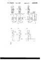
- FIG. 1is a block diagram showing an embodiment of a parallel transmission system according to the present invention
- FIG. 2is a circuit diagram showing the detail of the delay difference compensation circuit shown in FIG. 1;
- FIG. 3is a view used for explaining a prior art system
- FIG. 4is a view used for explaining the coding rule of line codes
- FIG. 5shows an example of transmission frames
- FIG. 6is a timing chart illustrating the operation of the embodiment shown in FIG. 1;
- FIG. 7is a timing chart used for explaining the operation of delay compensation.
- FIG. 1signals separated in parallel are applied to input terminals 1a to 1c.
- the signalsare converted into block coded line codes at line coders 3a to 3c, in accordance with block timing clocks supplied from an input terminal 2.
- the converted line codesare delivered to transmission lines 4a to 4c with the phase of each pulse block being made coincident with each other.
- the number of pulses of a single blockis selected as a number of 3 to 10 considering the efficient use of the bandwidth and the stable delay difference compensation.
- the line codesare assumed here as 2B3B line codes (2 bit words, 3 bit blocks).
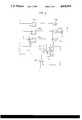
- the block time codesare regenerated by using receiver circuits 5a to 5c and timing circuits 6a to 6c. Since timing signals derived from the transmission lines are used in this operation, degradation of waveform margin for pulse regeneration is small. Differences of delays among outputs of the receiver circuits 5a to 5c occur, as shown by waveforms of FIG. 6(a) to FIG. 6(c).
- each output of the receiver circuit 5a to 5cis temporarily stored in delay difference compensation circuits 7a to 7c and thereafter, the phases of read-out pulse blocks are made equal to each other using a reference clock signal (represented by waveform of FIG. 6(d)) from a block timing circuit 8 (as shown by waveforms of FIG. 6(a') to FIG. 6(c')).
- a reference clock signalrepresented by waveform of FIG. 6(d)
- a block timing circuit 8as shown by waveforms of FIG. 6(a') to FIG. 6(c')
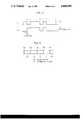
- a pulse stream (having waveform of FIG. 7(a)) applied to an input terminal 11is written into buffer memories constructed of flip-flops 15a1 to 15a3 as shown by waveforms of FIGS. 7(a1), 7(a2) and 7(a3), by using three-phase clock pulses (waveforms of FIGS. 7(u), 7(v) and 7(w)) supplied from input terminals 12 to 14.
- the stored signalsare read through gates 16a1 to 16a3 and 17 to result in a delay compensated signal (FIG. 7(a')).
- Three-phase read pulsesare generated from a ring counter 18 which is driven by pulses applied through a terminal 19 via a gate 20.
- the pulses applied from the gates 20 through 22are used for adjusting phases so that the phase of the pulse with the first phase ⁇ 1 coincides with that of the reference clock signal (waveform of FIG. 7(s) outputted form the block timing circuit 8) applied to input terminal 21.
- a clock signal for block synchronization which is sent from a sending side via another transmission line or reproduced at the receiving side,may be used as the reference clock signal.
Landscapes
- Engineering & Computer Science (AREA)
- Computer Networks & Wireless Communication (AREA)
- Signal Processing (AREA)
- Power Engineering (AREA)
- Synchronisation In Digital Transmission Systems (AREA)
- Dc Digital Transmission (AREA)
Abstract
Description
The present invention relates to a parallel transmission system for transmitting pulses distributed in parallel.
Conventionally, differences in delay times in transmission lines when transmitting pulses in parallel through the lines have been a problem. In order to solve this problem, various systems have been studied. One system is a so-called clock sharing system wherein pulses are regenerated using an average value of phases derived from the timing information obtained from transmission lines (Hitachi Journal Vol. 47, No. 3 (1965), pp. 102 to 113 "Time Division Multiplex PCM Communication System by Pulse Distribution Transmission").
However, as the bit rate becomes high, a difference in delay causes a more adverse effect, resulting in a degradation of waveform margin for pulse regeneration, an increase in bit error rates, or the like.
Such a situation will be described with reference to FIG. 3. In FIG. 3, three pulse trains are simultaneously transmitted fromtransmitters 21a to 21c over transmission lines 22a to 22c toreceivers 23a to 23c. The pulse trains are received at thereceivers 23a to 23c at different times because of the presence of different propagation delays in the transmission lines 22a to 22c, as shown in waveforms (a) to (c) in FIG. 3. In such a case, the received pulses are sampled by a clock pulse (d) to align them at a smae pulse regeneration time as shown by a dotted-line. However, this becomes difficult when pulse transmission is performed at higher bit rates.
For waveforms (a') to (c') at a bit rate two times as high as that of the waveforms (a) to (c), i.e., with a pulse width half that of the latter waveforms, it now becomes impossible to share a sampling pulse.
In order to solve the above problem, another method may be used wherein a signal is converted into a CMI (Coded Mark Inversion) code as shown in FIG. 4(a). Coding rule violation (indicated by an arrow in FIG. 4(b)) is applied to each signal at the sending side at the same time. The receiving side detects this coding rule violation to align or make equal the occurrence times of such violation at each signal by using buffer memories. With this method, however, a twofold bandwidth becomes necessary so that the circuit performance or the like may often hinder a high speed transmission and hence degrade signal regeneration.
For avoiding the use of a broad bandwidth, a method of insertingframe pulses 50 at constant intervals as illustrated in FIG. 5 is known. With this method, circuits fordiscriminating frame pulses 50 and information pulses are required, thus leading to a large size circuit arrangement.
An object of this invention is to solve the above problems and provide a parallel transmission system which ensures waveform margin for pulse regeneration at higher transmission speed, a high efficiency of bandwidth utilization, and is capable of delay compensation with simple circuitry.
In order to attain the above object, the present invention incorporates a specific characteristic of line codes. A block coding type (mBnB Line Code) is adopted as a line coding type, and the phase of each block is used as a basis for compensation of delay differences in parallel transmission.
Codes of a block coding type are obtained by coding original signals through division into blocks of the same length. This will be explained using a simple example: Original signals are divided into three bit words 100, 111, 101, 000, . . . and converted into four bit blocks by adding 1 or 0 after the last bit of each word. In accordance with a bit addition rule, one bit is added such that a difference of the numbers of 0s and 1s becomes smaller in each block. In the above example, the blocks are changed to 1001, 1110, 1010, 0001, . . . which are converted from three bit words to four bit blocks and hence called 3B4B codes.
To use the bandwidth effectively, it is necessary that a substantially large m/n (e.g., m/n≧2/3) and long block length (e.g., three bits or more) be used.
FIG. 1 is a block diagram showing an embodiment of a parallel transmission system according to the present invention;
FIG. 2 is a circuit diagram showing the detail of the delay difference compensation circuit shown in FIG. 1;
FIG. 3 is a view used for explaining a prior art system;
FIG. 4 is a view used for explaining the coding rule of line codes;
FIG. 5 shows an example of transmission frames;
FIG. 6 is a timing chart illustrating the operation of the embodiment shown in FIG. 1; and
FIG. 7 is a timing chart used for explaining the operation of delay compensation.
An embodiment of the present invention will now be described with reference to FIG. 1. In FIG. 1, signals separated in parallel are applied to input terminals 1a to 1c. The signals are converted into block coded line codes atline coders 3a to 3c, in accordance with block timing clocks supplied from aninput terminal 2. The converted line codes are delivered to transmission lines 4a to 4c with the phase of each pulse block being made coincident with each other. Typically, the number of pulses of a single block is selected as a number of 3 to 10 considering the efficient use of the bandwidth and the stable delay difference compensation. The line codes are assumed here as 2B3B line codes (2 bit words, 3 bit blocks).
On the receiving side, the block time codes are regenerated by using receiver circuits 5a to 5c andtiming circuits 6a to 6c. Since timing signals derived from the transmission lines are used in this operation, degradation of waveform margin for pulse regeneration is small. Differences of delays among outputs of the receiver circuits 5a to 5c occur, as shown by waveforms of FIG. 6(a) to FIG. 6(c).
In order to compensate for the delay difference, each output of the receiver circuit 5a to 5c is temporarily stored in delaydifference compensation circuits 7a to 7c and thereafter, the phases of read-out pulse blocks are made equal to each other using a reference clock signal (represented by waveform of FIG. 6(d)) from a block timing circuit 8 (as shown by waveforms of FIG. 6(a') to FIG. 6(c')). After compensating for the delay difference, the block line codes are reconnected into the original signals.
The operation of the delaydifference compensation circuits 7a-c will be described with reference to FIG. 2. It is assumed that the line codes used in this circuit are 2B3B line codes comprising three bits per one block. A pulse stream (having waveform of FIG. 7(a)) applied to an input terminal 11 is written into buffer memories constructed of flip-flops 15a1 to 15a3 as shown by waveforms of FIGS. 7(a1), 7(a2) and 7(a3), by using three-phase clock pulses (waveforms of FIGS. 7(u), 7(v) and 7(w)) supplied frominput terminals 12 to 14. The stored signals are read through gates 16a1 to 16a3 and 17 to result in a delay compensated signal (FIG. 7(a')). Three-phase read pulses (waveforms of FIGS. 7(x), 7(y) and 7(z)) are generated from aring counter 18 which is driven by pulses applied through aterminal 19 via agate 20. The pulses applied from thegates 20 through 22 are used for adjusting phases so that the phase of the pulse with the first phase φ1 coincides with that of the reference clock signal (waveform of FIG. 7(s) outputted form the block timing circuit 8) applied toinput terminal 21.
A clock signal for block synchronization which is sent from a sending side via another transmission line or reproduced at the receiving side, may be used as the reference clock signal.
As described above, according to the present invention, degradation of waveform margin for pulse regeneration due to delay difference is not caused even at high speed parallel transmission if a substantially long block length (e.g., 3 to 10 bits) is used. Further, the line code is effectively used for alignment of the phases of pulse blocks with the help of simple block timing circuit, which leads to economical system realization.
Claims (9)
1. A parallel transmission system comprising:
a plurality of line coders for converting parallel original signals into parallel mBnB line codes, each code including a series of n-bit blocks, and each block including an m-bit word, where m and n are natural numbers;
a block timing clock signal for aligning phases of the blocks of said mBnB line codes;
a plurality of parallel transmission lines for transmitting said parallel mBnB line codes from said line codes wherein each transmission line transmits an mBnB line code;
a plurality of receiver circuits for receiving said parallel mBnB line codes from said line coders; and
delay difference compensation means for aligning the phases of the blocks of the parallel mBnB line codes received by said receiver circuits based on a reference signal.
2. A parallel transmission system comprising:
means for converting parallel original signals into parallel mBnB line codes each code including a series of n-bit blocks, each block including an m-bit word and the phases of the blocks of said mBnB line codes being aligned;
means connected to said converting means for receiving said parallel mBnB line codes through parallel transmission lines; and
means for aligning the phases of the blocks of said received parallel mBnB line codes based on a reference signal.
3. A parallel transmission method comprising the steps of:
converting parallel original signals into parallel mBnB line codes each code including a series of n-bit blocks, and each block including an m-bit word;
aligning the phases of the blocks of said parallel mBnB line codes;
transmitting said mBnB line codes with the phases having been aligned with one another;
receiving each mBnB line code after the transmitting step; and
aligning the phases of the blocks of the received parallel mBnB line codes based on a reference signal.
4. A parallel transmission method according to claim 3, wherein said reference signal is generated at the receiving side independently.
5. A parallel transmission method according to claim 3, where said reference signal is a clock signal for block synchronization and said reference signal is sent from the sending side via another transmission line.
6. A parallel transmission method according to claim 3, wherein said reference signal is a clock signal for block synchronization generated at the receiving side.
7. A parallel transmission system according to claim 1, wherein n is a natural number where 3≦n≦10.
8. A parallel transmission system according to claim 2, wherein n is a natural number where 3≦n≦10.
9. A parallel transmission method according to claim 3, wherein n is a natural number where 3≦n≦10.
Applications Claiming Priority (2)
| Application Number | Priority Date | Filing Date | Title |
|---|---|---|---|
| JP11263186AJPH07105818B2 (en) | 1986-05-19 | 1986-05-19 | Parallel transmission method |
| JP61-112631 | 1987-05-19 |
Publications (1)
| Publication Number | Publication Date |
|---|---|
| US4818995Atrue US4818995A (en) | 1989-04-04 |
Family
ID=14591560
Family Applications (1)
| Application Number | Title | Priority Date | Filing Date |
|---|---|---|---|
| US07/051,519Expired - Fee RelatedUS4818995A (en) | 1986-05-19 | 1987-05-19 | Parallel transmission system |
Country Status (4)
| Country | Link |
|---|---|
| US (1) | US4818995A (en) |
| JP (1) | JPH07105818B2 (en) |
| CA (1) | CA1289249C (en) |
| GB (1) | GB2191662B (en) |
Cited By (32)
| Publication number | Priority date | Publication date | Assignee | Title |
|---|---|---|---|---|
| US5251210A (en)* | 1991-11-01 | 1993-10-05 | Ibm Corporation | Method and apparatus for transforming low bandwidth telecommunications channels into a high bandwidth telecommunication channel |
| US5253254A (en)* | 1991-09-18 | 1993-10-12 | Dsc Communications Corporation | Telecommunications system with arbitrary alignment parallel framer |
| US5255287A (en)* | 1991-06-28 | 1993-10-19 | Digital Equipment Corporation | Transceiver apparatus and methods |
| US5293626A (en)* | 1990-06-08 | 1994-03-08 | Cray Research, Inc. | Clock distribution apparatus and processes particularly useful in multiprocessor systems |
| US5341405A (en)* | 1991-06-11 | 1994-08-23 | Digital Equipment Corporation | Data recovery apparatus and methods |
| US5363378A (en)* | 1992-04-07 | 1994-11-08 | U.S. Philips Corporation | Channel data transmission system |
| US5379299A (en)* | 1992-04-16 | 1995-01-03 | The Johns Hopkins University | High speed propagation delay compensation network |
| US5408473A (en)* | 1992-03-03 | 1995-04-18 | Digital Equipment Corporation | Method and apparatus for transmission of communication signals over two parallel channels |
| US5412691A (en)* | 1991-06-28 | 1995-05-02 | Digital Equipment Corporation | Method and apparatus for equalization for transmission over a band-limited channel |
| US5430733A (en)* | 1988-12-28 | 1995-07-04 | Hitachi, Ltd. | Digital transmission system for multiplexing and demultiplexing signals |
| US5442457A (en)* | 1993-01-11 | 1995-08-15 | Najafi; Hamid | Multi-line pooling facsimile apparatus |
| US5455831A (en)* | 1992-02-20 | 1995-10-03 | International Business Machines Corporation | Frame group transmission and reception for parallel/serial buses |
| US5598442A (en)* | 1994-06-17 | 1997-01-28 | International Business Machines Corporation | Self-timed parallel inter-system data communication channel |
| WO2001019044A1 (en)* | 1999-09-03 | 2001-03-15 | Infineon Technologies Ag | Device and method for compensating for propagation delay |
| US6256259B1 (en) | 1997-03-05 | 2001-07-03 | Micron Technology, Inc. | Delay-locked loop with binary-coupled capacitor |
| US6269451B1 (en) | 1998-02-27 | 2001-07-31 | Micron Technology, Inc. | Method and apparatus for adjusting data timing by delaying clock signal |
| US6279090B1 (en) | 1998-09-03 | 2001-08-21 | Micron Technology, Inc. | Method and apparatus for resynchronizing a plurality of clock signals used in latching respective digital signals applied to a packetized memory device |
| US20010024135A1 (en)* | 1997-06-20 | 2001-09-27 | Harrison Ronnie M. | Method and apparatus for generating a sequence of clock signals |
| US6338127B1 (en) | 1998-08-28 | 2002-01-08 | Micron Technology, Inc. | Method and apparatus for resynchronizing a plurality of clock signals used to latch respective digital signals, and memory device using same |
| US6340904B1 (en) | 1997-02-11 | 2002-01-22 | Micron Technology, Inc. | Method and apparatus for generating an internal clock signal that is synchronized to an external clock signal |
| US6349399B1 (en) | 1998-09-03 | 2002-02-19 | Micron Technology, Inc. | Method and apparatus for generating expect data from a captured bit pattern, and memory device using same |
| US6374360B1 (en) | 1998-12-11 | 2002-04-16 | Micron Technology, Inc. | Method and apparatus for bit-to-bit timing correction of a high speed memory bus |
| US6430696B1 (en)* | 1998-11-30 | 2002-08-06 | Micron Technology, Inc. | Method and apparatus for high speed data capture utilizing bit-to-bit timing correction, and memory device using same |
| US6441666B1 (en) | 2000-07-20 | 2002-08-27 | Silicon Graphics, Inc. | System and method for generating clock signals |
| US6647028B1 (en) | 1997-09-30 | 2003-11-11 | Cisco Technology, Inc. | System and method for recovering and restoring lost data in a N-channel coherent data transmission system |
| US20040103226A1 (en)* | 2001-06-28 | 2004-05-27 | Brian Johnson | Method and system for adjusting the timing offset between a clock signal and respective digital signals transmitted along with clock signal, and memory device and computer system using same |
| US20050091464A1 (en)* | 2003-10-27 | 2005-04-28 | Ralph James | System and method for using a learning sequence to establish communications on a high-speed nonsynchronous interface in the absence of clock forwarding |
| US6912680B1 (en) | 1997-02-11 | 2005-06-28 | Micron Technology, Inc. | Memory system with dynamic timing correction |
| US6931086B2 (en) | 1999-03-01 | 2005-08-16 | Micron Technology, Inc. | Method and apparatus for generating a phase dependent control signal |
| US6959016B1 (en) | 1997-09-18 | 2005-10-25 | Micron Technology, Inc. | Method and apparatus for adjusting the timing of signals over fine and coarse ranges |
| US7168027B2 (en) | 2003-06-12 | 2007-01-23 | Micron Technology, Inc. | Dynamic synchronization of data capture on an optical or other high speed communications link |
| US7676725B1 (en) | 2006-02-27 | 2010-03-09 | The United States Of America As Represented By The Director, National Security Agency | Method of code generation that minimizes error propagation |
Families Citing this family (6)
| Publication number | Priority date | Publication date | Assignee | Title |
|---|---|---|---|---|
| JP2684815B2 (en)* | 1990-04-17 | 1997-12-03 | 日立電線株式会社 | Digital multiplex transmission system |
| JP3158213B2 (en)* | 1991-09-12 | 2001-04-23 | 富士通株式会社 | Parallel transmission method and apparatus |
| GB9314479D0 (en)* | 1992-11-06 | 1993-08-25 | Hewlett Packard Co | Encoding data |
| US5396503A (en)* | 1993-02-19 | 1995-03-07 | Hewlett-Packard Company | Method and system for communicating data |
| GB9314480D0 (en)* | 1993-07-09 | 1993-08-25 | Hewlett Packard Co | Encoding data |
| WO2017033318A1 (en)* | 2015-08-26 | 2017-03-02 | 堺ディスプレイプロダクト株式会社 | Data transmitting and receiving device, and display device |
Citations (3)
| Publication number | Priority date | Publication date | Assignee | Title |
|---|---|---|---|---|
| US4520480A (en)* | 1982-05-18 | 1985-05-28 | Nec Corporation | Digital transmission system |
| US4615040A (en)* | 1984-06-14 | 1986-09-30 | Coenco Ltd. | High speed data communications system |
| US4691294A (en)* | 1984-09-21 | 1987-09-01 | International Computers Limited | Clock/data synchronization interface apparatus and method |
Family Cites Families (2)
| Publication number | Priority date | Publication date | Assignee | Title |
|---|---|---|---|---|
| JPS615656A (en)* | 1984-06-20 | 1986-01-11 | Nec Corp | Separation transmitting system of digital signal |
| GB8528890D0 (en)* | 1985-11-23 | 1986-01-02 | Int Computers Ltd | Data transmission system |
- 1986
- 1986-05-19JPJP11263186Apatent/JPH07105818B2/ennot_activeExpired - Fee Related
- 1987
- 1987-05-15GBGB8711584Apatent/GB2191662B/ennot_activeExpired - Lifetime
- 1987-05-19USUS07/051,519patent/US4818995A/ennot_activeExpired - Fee Related
- 1987-05-19CACA000537414Apatent/CA1289249C/ennot_activeExpired
Patent Citations (3)
| Publication number | Priority date | Publication date | Assignee | Title |
|---|---|---|---|---|
| US4520480A (en)* | 1982-05-18 | 1985-05-28 | Nec Corporation | Digital transmission system |
| US4615040A (en)* | 1984-06-14 | 1986-09-30 | Coenco Ltd. | High speed data communications system |
| US4691294A (en)* | 1984-09-21 | 1987-09-01 | International Computers Limited | Clock/data synchronization interface apparatus and method |
Cited By (75)
| Publication number | Priority date | Publication date | Assignee | Title |
|---|---|---|---|---|
| US5430733A (en)* | 1988-12-28 | 1995-07-04 | Hitachi, Ltd. | Digital transmission system for multiplexing and demultiplexing signals |
| US5293626A (en)* | 1990-06-08 | 1994-03-08 | Cray Research, Inc. | Clock distribution apparatus and processes particularly useful in multiprocessor systems |
| US5341405A (en)* | 1991-06-11 | 1994-08-23 | Digital Equipment Corporation | Data recovery apparatus and methods |
| US5255287A (en)* | 1991-06-28 | 1993-10-19 | Digital Equipment Corporation | Transceiver apparatus and methods |
| US5412691A (en)* | 1991-06-28 | 1995-05-02 | Digital Equipment Corporation | Method and apparatus for equalization for transmission over a band-limited channel |
| US5253254A (en)* | 1991-09-18 | 1993-10-12 | Dsc Communications Corporation | Telecommunications system with arbitrary alignment parallel framer |
| US5251210A (en)* | 1991-11-01 | 1993-10-05 | Ibm Corporation | Method and apparatus for transforming low bandwidth telecommunications channels into a high bandwidth telecommunication channel |
| US5455831A (en)* | 1992-02-20 | 1995-10-03 | International Business Machines Corporation | Frame group transmission and reception for parallel/serial buses |
| US5408473A (en)* | 1992-03-03 | 1995-04-18 | Digital Equipment Corporation | Method and apparatus for transmission of communication signals over two parallel channels |
| US5363378A (en)* | 1992-04-07 | 1994-11-08 | U.S. Philips Corporation | Channel data transmission system |
| US5379299A (en)* | 1992-04-16 | 1995-01-03 | The Johns Hopkins University | High speed propagation delay compensation network |
| US5442457A (en)* | 1993-01-11 | 1995-08-15 | Najafi; Hamid | Multi-line pooling facsimile apparatus |
| US5598442A (en)* | 1994-06-17 | 1997-01-28 | International Business Machines Corporation | Self-timed parallel inter-system data communication channel |
| US5651033A (en)* | 1994-06-17 | 1997-07-22 | International Business Machines Corporation | Inter-system data communication channel comprised of parallel electrical conductors that simulates the performance of a bit serial optical communications link |
| US6340904B1 (en) | 1997-02-11 | 2002-01-22 | Micron Technology, Inc. | Method and apparatus for generating an internal clock signal that is synchronized to an external clock signal |
| US6912680B1 (en) | 1997-02-11 | 2005-06-28 | Micron Technology, Inc. | Memory system with dynamic timing correction |
| US6256259B1 (en) | 1997-03-05 | 2001-07-03 | Micron Technology, Inc. | Delay-locked loop with binary-coupled capacitor |
| US6490207B2 (en) | 1997-03-05 | 2002-12-03 | Micron Technology, Inc. | Delay-locked loop with binary-coupled capacitor |
| US6490224B2 (en) | 1997-03-05 | 2002-12-03 | Micron Technology, Inc. | Delay-locked loop with binary-coupled capacitor |
| US6483757B2 (en) | 1997-03-05 | 2002-11-19 | Micron Technology, Inc. | Delay-locked loop with binary-coupled capacitor |
| US6400641B1 (en) | 1997-03-05 | 2002-06-04 | Micron Technology, Inc. | Delay-locked loop with binary-coupled capacitor |
| US20010024135A1 (en)* | 1997-06-20 | 2001-09-27 | Harrison Ronnie M. | Method and apparatus for generating a sequence of clock signals |
| US7889593B2 (en) | 1997-06-20 | 2011-02-15 | Round Rock Research, Llc | Method and apparatus for generating a sequence of clock signals |
| US7415404B2 (en) | 1997-06-20 | 2008-08-19 | Micron Technology, Inc. | Method and apparatus for generating a sequence of clock signals |
| US8565008B2 (en) | 1997-06-20 | 2013-10-22 | Round Rock Research, Llc | Method and apparatus for generating a sequence of clock signals |
| US20080126059A1 (en)* | 1997-06-20 | 2008-05-29 | Micron Technology, Inc. | Method and apparatus for generating a sequence of clock signals |
| US20050249028A1 (en)* | 1997-06-20 | 2005-11-10 | Harrison Ronnie M | Method and apparatus for generating a sequence of clock signals |
| US6954097B2 (en) | 1997-06-20 | 2005-10-11 | Micron Technology, Inc. | Method and apparatus for generating a sequence of clock signals |
| US20110122710A1 (en)* | 1997-06-20 | 2011-05-26 | Round Rock Research, Llc | Method and apparatus for generating a sequence of clock signals |
| US6959016B1 (en) | 1997-09-18 | 2005-10-25 | Micron Technology, Inc. | Method and apparatus for adjusting the timing of signals over fine and coarse ranges |
| US6647028B1 (en) | 1997-09-30 | 2003-11-11 | Cisco Technology, Inc. | System and method for recovering and restoring lost data in a N-channel coherent data transmission system |
| US6269451B1 (en) | 1998-02-27 | 2001-07-31 | Micron Technology, Inc. | Method and apparatus for adjusting data timing by delaying clock signal |
| US6499111B2 (en) | 1998-02-27 | 2002-12-24 | Micron Technology, Inc. | Apparatus for adjusting delay of a clock signal relative to a data signal |
| US6327196B1 (en) | 1998-02-27 | 2001-12-04 | Micron Technology, Inc. | Synchronous memory device having an adjustable data clocking circuit |
| US6643789B2 (en) | 1998-02-27 | 2003-11-04 | Micron Technology, Inc. | Computer system having memory device with adjustable data clocking using pass gates |
| US6378079B1 (en) | 1998-02-27 | 2002-04-23 | Micron Technology, Inc. | Computer system having memory device with adjustable data clocking |
| US6338127B1 (en) | 1998-08-28 | 2002-01-08 | Micron Technology, Inc. | Method and apparatus for resynchronizing a plurality of clock signals used to latch respective digital signals, and memory device using same |
| US6647523B2 (en) | 1998-09-03 | 2003-11-11 | Micron Technology, Inc. | Method for generating expect data from a captured bit pattern, and memory device using same |
| US7085975B2 (en) | 1998-09-03 | 2006-08-01 | Micron Technology, Inc. | Method and apparatus for generating expect data from a captured bit pattern, and memory device using same |
| US20040158785A1 (en)* | 1998-09-03 | 2004-08-12 | Manning Troy A. | Method and apparatus for generating expect data from a captured bit pattern, and memory device using same |
| US7657813B2 (en) | 1998-09-03 | 2010-02-02 | Micron Technology, Inc. | Method and apparatus for generating expect data from a captured bit pattern, and memory device using same |
| US20080195908A1 (en)* | 1998-09-03 | 2008-08-14 | Micron Technology, Inc. | Method and apparatus for generating expect data from a captured bit pattern, and memory device using same |
| US7373575B2 (en) | 1998-09-03 | 2008-05-13 | Micron Technology, Inc. | Method and apparatus for generating expect data from a captured bit pattern, and memory device using same |
| US20100106997A1 (en)* | 1998-09-03 | 2010-04-29 | Micron Technology, Inc. | Method and apparatus for generating expect data from a captured bit pattern, and memory device using same |
| US6349399B1 (en) | 1998-09-03 | 2002-02-19 | Micron Technology, Inc. | Method and apparatus for generating expect data from a captured bit pattern, and memory device using same |
| US6279090B1 (en) | 1998-09-03 | 2001-08-21 | Micron Technology, Inc. | Method and apparatus for resynchronizing a plurality of clock signals used in latching respective digital signals applied to a packetized memory device |
| US6477675B2 (en) | 1998-09-03 | 2002-11-05 | Micron Technology, Inc. | Method and apparatus for generating expect data from a captured bit pattern, and memory device using same |
| US7954031B2 (en) | 1998-09-03 | 2011-05-31 | Round Rock Research, Llc | Method and apparatus for generating expect data from a captured bit pattern, and memory device using same |
| US6430696B1 (en)* | 1998-11-30 | 2002-08-06 | Micron Technology, Inc. | Method and apparatus for high speed data capture utilizing bit-to-bit timing correction, and memory device using same |
| US6374360B1 (en) | 1998-12-11 | 2002-04-16 | Micron Technology, Inc. | Method and apparatus for bit-to-bit timing correction of a high speed memory bus |
| US6662304B2 (en) | 1998-12-11 | 2003-12-09 | Micron Technology, Inc. | Method and apparatus for bit-to-bit timing correction of a high speed memory bus |
| US20050286505A1 (en)* | 1999-03-01 | 2005-12-29 | Harrison Ronnie M | Method and apparatus for generating a phase dependent control signal |
| US8107580B2 (en) | 1999-03-01 | 2012-01-31 | Round Rock Research, Llc | Method and apparatus for generating a phase dependent control signal |
| US6952462B2 (en) | 1999-03-01 | 2005-10-04 | Micron Technology, Inc. | Method and apparatus for generating a phase dependent control signal |
| US6931086B2 (en) | 1999-03-01 | 2005-08-16 | Micron Technology, Inc. | Method and apparatus for generating a phase dependent control signal |
| US7602876B2 (en) | 1999-03-01 | 2009-10-13 | Micron Technology, Inc. | Method and apparatus for generating a phase dependent control signal |
| US8433023B2 (en) | 1999-03-01 | 2013-04-30 | Round Rock Research, Llc | Method and apparatus for generating a phase dependent control signal |
| US7016451B2 (en) | 1999-03-01 | 2006-03-21 | Micron Technology, Inc. | Method and apparatus for generating a phase dependent control signal |
| US7418071B2 (en) | 1999-03-01 | 2008-08-26 | Micron Technology, Inc. | Method and apparatus for generating a phase dependent control signal |
| US20080279323A1 (en)* | 1999-03-01 | 2008-11-13 | Harrison Ronnie M | Method and apparatus for generating a phase dependent control signal |
| US6583737B2 (en) | 1999-09-03 | 2003-06-24 | Infineon Technologies Ag | Device and method for compensating for propagation delay |
| WO2001019044A1 (en)* | 1999-09-03 | 2001-03-15 | Infineon Technologies Ag | Device and method for compensating for propagation delay |
| US6441666B1 (en) | 2000-07-20 | 2002-08-27 | Silicon Graphics, Inc. | System and method for generating clock signals |
| US7159092B2 (en) | 2001-06-28 | 2007-01-02 | Micron Technology, Inc. | Method and system for adjusting the timing offset between a clock signal and respective digital signals transmitted along with that clock signal, and memory device and computer system using same |
| US20040103226A1 (en)* | 2001-06-28 | 2004-05-27 | Brian Johnson | Method and system for adjusting the timing offset between a clock signal and respective digital signals transmitted along with clock signal, and memory device and computer system using same |
| US6801989B2 (en) | 2001-06-28 | 2004-10-05 | Micron Technology, Inc. | Method and system for adjusting the timing offset between a clock signal and respective digital signals transmitted along with that clock signal, and memory device and computer system using same |
| US20080301533A1 (en)* | 2003-06-12 | 2008-12-04 | Micron Technology, Inc. | Dynamic synchronization of data capture on an optical or other high speed communications link |
| US7168027B2 (en) | 2003-06-12 | 2007-01-23 | Micron Technology, Inc. | Dynamic synchronization of data capture on an optical or other high speed communications link |
| US8181092B2 (en) | 2003-06-12 | 2012-05-15 | Round Rock Research, Llc | Dynamic synchronization of data capture on an optical or other high speed communications link |
| US8892974B2 (en) | 2003-06-12 | 2014-11-18 | Round Rock Research, Llc | Dynamic synchronization of data capture on an optical or other high speed communications link |
| US7461286B2 (en) | 2003-10-27 | 2008-12-02 | Micron Technology, Inc. | System and method for using a learning sequence to establish communications on a high-speed nonsynchronous interface in the absence of clock forwarding |
| US7234070B2 (en) | 2003-10-27 | 2007-06-19 | Micron Technology, Inc. | System and method for using a learning sequence to establish communications on a high-speed nonsynchronous interface in the absence of clock forwarding |
| US20060206742A1 (en)* | 2003-10-27 | 2006-09-14 | Ralph James | System and method for using a learning sequence to establish communications on a high- speed nonsynchronous interface in the absence of clock forwarding |
| US20050091464A1 (en)* | 2003-10-27 | 2005-04-28 | Ralph James | System and method for using a learning sequence to establish communications on a high-speed nonsynchronous interface in the absence of clock forwarding |
| US7676725B1 (en) | 2006-02-27 | 2010-03-09 | The United States Of America As Represented By The Director, National Security Agency | Method of code generation that minimizes error propagation |
Also Published As
| Publication number | Publication date |
|---|---|
| GB2191662A (en) | 1987-12-16 |
| JPS62269443A (en) | 1987-11-21 |
| GB2191662B (en) | 1990-09-12 |
| GB8711584D0 (en) | 1987-06-17 |
| JPH07105818B2 (en) | 1995-11-13 |
| CA1289249C (en) | 1991-09-17 |
Similar Documents
| Publication | Publication Date | Title |
|---|---|---|
| US4818995A (en) | Parallel transmission system | |
| US4584690A (en) | Alternate Mark Invert (AMI) transceiver with switchable detection and digital precompensation | |
| US4602365A (en) | Multi-token, multi-channel single bus network | |
| US6449315B2 (en) | Serial line synchronization method and apparatus | |
| JPH0477494B2 (en) | ||
| CA2251372A1 (en) | System and method for high-speed skew-insensitive multi-channel data transmission | |
| EP0016336B1 (en) | Digital signal transmission system | |
| US3953673A (en) | Digital data signalling systems and apparatus therefor | |
| EP0312260A2 (en) | A high-speed demultiplexer circuit | |
| US4516236A (en) | Full-duplex transmission of bit streams serially and in bit-synchronism on a bus between two terminals. | |
| US4551830A (en) | Apparatus for providing loopback of signals where the signals being looped back have an overhead data format which is incompatible with a high speed intermediate carrier overhead format | |
| US4486740A (en) | DC Cancellation in ternary-coded data systems | |
| US4498167A (en) | TDM Communication system | |
| US5430733A (en) | Digital transmission system for multiplexing and demultiplexing signals | |
| US4736372A (en) | Method and apparatus of transmission for a digital signal | |
| US3939307A (en) | Arrangement for utilizing all pulses in a narrow band channel of a time-division multiplex, pulse code modulation system | |
| EP0409168B1 (en) | Elastic store memory circuit | |
| US4796281A (en) | Digital signal transmission system | |
| JPS6320931A (en) | Data transmission equipment | |
| US4346259A (en) | Low speed terminal interface for all-digital PABX | |
| GB1362653A (en) | Data network terminal unit | |
| JPS61253958A (en) | Digital communication system | |
| JPS58114542A (en) | Code converting circuit | |
| JPS61125240A (en) | System split system in pcm communication | |
| JPH01101749A (en) | Method for transmitting auxiliary signal |
Legal Events
| Date | Code | Title | Description |
|---|---|---|---|
| AS | Assignment | Owner name:NIPPON TELEGRAPH AND TELEPHONE CORPORATION, 1-6, U Free format text:ASSIGNMENT OF ASSIGNORS INTEREST.;ASSIGNORS:TAKASAKI, YOSHITAKA;TAKAHASHI, YASUSHI;NAKANO, YUKIO;AND OTHERS;REEL/FRAME:004737/0778 Effective date:19870526 Owner name:HITACHI, LTD., 6, KANDA SURUGADAI 4-CHOME, CHIYODA Free format text:ASSIGNMENT OF ASSIGNORS INTEREST.;ASSIGNORS:TAKASAKI, YOSHITAKA;TAKAHASHI, YASUSHI;NAKANO, YUKIO;AND OTHERS;REEL/FRAME:004737/0778 Effective date:19870526 | |
| FPAY | Fee payment | Year of fee payment:4 | |
| FEPP | Fee payment procedure | Free format text:PAYOR NUMBER ASSIGNED (ORIGINAL EVENT CODE: ASPN); ENTITY STATUS OF PATENT OWNER: LARGE ENTITY | |
| FPAY | Fee payment | Year of fee payment:8 | |
| REMI | Maintenance fee reminder mailed | ||
| LAPS | Lapse for failure to pay maintenance fees | ||
| FP | Lapsed due to failure to pay maintenance fee | Effective date:20010404 | |
| STCH | Information on status: patent discontinuation | Free format text:PATENT EXPIRED DUE TO NONPAYMENT OF MAINTENANCE FEES UNDER 37 CFR 1.362 |