US4816997A - Bus master having selective burst deferral - Google Patents
Bus master having selective burst deferralDownload PDFInfo
- Publication number
- US4816997A US4816997AUS07/099,359US9935987AUS4816997AUS 4816997 AUS4816997 AUS 4816997AUS 9935987 AUS9935987 AUS 9935987AUS 4816997 AUS4816997 AUS 4816997A
- Authority
- US
- United States
- Prior art keywords
- burst
- cache
- bus master
- signal
- deferral
- Prior art date
- Legal status (The legal status is an assumption and is not a legal conclusion. Google has not performed a legal analysis and makes no representation as to the accuracy of the status listed.)
- Expired - Lifetime
Links
Images


Classifications
- G—PHYSICS
- G11—INFORMATION STORAGE
- G11C—STATIC STORES
- G11C7/00—Arrangements for writing information into, or reading information out from, a digital store
- G—PHYSICS
- G06—COMPUTING OR CALCULATING; COUNTING
- G06F—ELECTRIC DIGITAL DATA PROCESSING
- G06F12/00—Accessing, addressing or allocating within memory systems or architectures
- G06F12/02—Addressing or allocation; Relocation
- G06F12/08—Addressing or allocation; Relocation in hierarchically structured memory systems, e.g. virtual memory systems
- G06F12/0802—Addressing of a memory level in which the access to the desired data or data block requires associative addressing means, e.g. caches
- G06F12/0877—Cache access modes
- G06F12/0879—Burst mode
Definitions
- the subject inventionrelates generally to bus masters and, more particularly, to a bus master having a burst transfer mode of operation.
- each storage cellis individually accessed using a unique access address.
- several other storage cellsare accessed simultaneously and the contents thereof are held temporarily in a buffer.
- the access addresses of these "extra" storage cellsdiffer from the original access address by only one or two bits.
- subsequent accesses to these cellscan be accomplished by simply executing additional access cycles without changing the access address.
- such memoriesare referred to as "nibble mode".
- a portion of the original access addresscan be "assumed” for one (or more) subsequent accesses, so that only the least significant portion of the address needs to be decoded, etc.
- this burst mode of operationfacilitates fast filling of entire cache lines.
- the burst operationshould only be initiated if all of the entries in the cache line are invalid.
- a burst operationshould not be initiated if further data processing must be delayed in order to cache the nonessential entries in a cache line.
- the bus masterincludes a cache for storing a plurality of the operands in each of a plurality of cache lines; cache control logic for accessing the cache to determine if a selected operand is stored in the cache, and providing a cache hit signal if the selected operand is stored in the cache; burst deferral logic for determining that an operand to be transferred will span a plurality of the cache lines, and providing a burst deferral signal in response thereto; and burst control means for providing the burst request signal to the memory unless the cache control logic provides the cache hit signal or the burst deferral logic provides the burst deferral signal.
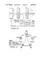
- FIG. 1illustrates in block diagram form, a data processing system having a bus master constructed in accordance with the present invention.
- FIG. 2illustrates in timing diagram form, the operation of the data processing system shown in FIG. 1.
- FIG. 3illustrates in block diagram form, the preferred form of the burst control logic of the bus master shown in FIG. 1.
- FIG. 4illustrates in state diagram form, the operation of the burst controller of the bus master shown in FIG. 3.
- FIG. 5illustrates the preferred form of the burst initiation logic.
- FIG. 6illustrates a modified form of the burst initiation logic of FIG. 5.
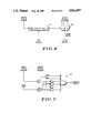
- FIG. 7illustrates the preferred form of the burst deferral logic.
- FIG. 1Shown in FIG. 1 is a data processing system 10 comprising a bus master 12 and a memory system 13 which is capable of transferring operands via a data bus 14 in bursts of m in response to a burst request (BREQ) signal provided by the bus master 12, the operands being clustered modulo m about a selected access address provided by the bus master 12 via an address bus 16, where m is two (2) to the n power, n being an integer and characteristic of the memory 13.
- BREQburst request
- an address register 18stores the access address for each operand which is to be transferred between the memory 13 and a buffer 20.
- a modulo-m adder 22is provided to increment, modulo m, an appropriate set n of the bits of the access address stored in the address register 18, in response to an increment (INC) signal provided by a burst controller 24.
- the burst controller 24will initially provide the BREQ signal to indicate to the memory 13 that the bus master 12 wishes for the memory 13 to continue after the current access cycle with the next operand in the burst. If at the end of the current access cycle the memory 13 decides that it can "burst" the next operand, it will so indicate by providing, substantially simultaneously, both a burst acknowledge (BACK) signal and a cycle termination (TERM) signal; otherwise, i simply provides the TERM signal.
- BACKburst acknowledge
- TRMcycle termination
- the burst controller 24In response to receiving both the BACK and the TERM signals, the burst controller 24 will again provide the BREQ signal to the memory 13. In addition, the burst controller 24 will provide, substantially simultaneously, the INC signal to the adder 22 to "sequence" the access address stored in the address register 18. In response to receiving just the TERM signal or after m-1 operands have been burst transferred, the burst controller 24 will cease to provide either the BREQ or the INC signals.
- FIG. 4illustrates in state diagram form the operation of the burst controller 24.
- a set associative cache 26 of conventional formwhich stores in each of a plurality of cache lines 28, a set of operands, an address tag (TAG) common to each of the operands in the cache line 28, and a set of valid (VALID) bits, each of which when SET indicates the validity of a respective one of the operands in the cache line 28.
- the cache 26is accessed in a conventional manner using tag (TAG), index (INDEX) and entry select (ENTRY) portions of an access address (ACCESS ADDRESS).
- TAG COMPARATOR 30will provide a TAG HIT signal.
- the VALID bit for the selected ENTRY in the INDEXed cache line 28is SET, AND gate 32 will provide an ENTRY HIT signal.
- the TAG HIT and ENTRY HIT signalsare used by cache control logic (not shown) to determine if an operand having the selected ACCESS ADDRESS is in the cache 26.
- a NAND gate 34 in the burst initiation logic 36will disable an AND gate 38 to prevent the burst start BRST signal (FIG. 3).
- NAND gate 34will also disable AND gate 38 in response to a VALID ENTRY signal provided by an OR gate 40 if any of the VALID bits in the INDEXed cache line 28 are SET.
- the BRST signalwill be provided by the AND gate 38 only if there is neither a TAG HIT signal nor a VALID ENTRY signal.
- FIG. 6Shown in FIG. 6 is a modified form of the valid entry detection portion of the burst initiation logic 36 of FIG. 5.
- the ENTRY portion of the ACCESS ADDRESSis incremented by a second, modulo-m adder 22' in response to the INC signal (FIG. 3), and applied to a 1-of-4 multiplexor 40' to select the VALID bit of the ENTRY in the INDEXed cache 28 line "following" (modulo 4) the selected ENTRY.
- the resulting VALID ENTRY signal provided by the multiplexor 40'may be applied to the NAND gate 34 in place of, or in some logical combination with, the VALID ENTRY signal provided by the OR gate 40 (FIG.
- the state diagram (FIG. 4) for the burst controller 24(FIG. 3) must be modified somewhat, so that the termination of the BRST signal after the burst operation has commenced will force the burst controller 24 back to the initial state.
- the burst initiation logic 36 of FIG. 5may attempt to burst fill the entire INDEX cache line 28 before initiating the filling of the INDEX+1 cache line 28.
- the full operandmay not be available until after the INDEX cache line 28 has been completely filled.
- burst deferral logic 42such as that shown in FIG. 7 may be provided to selectively disable the AND gate 38 (FIG. 5) via a DISABLE signal.
- the burst deferral logic 42will provide the DISABLE signal only if the ENTRY and BYTE select portions of the ACCESS ADDRESS (FIG. 5) and the operand SIZE signals (S1 and S0, encoded as in U.S. Pat. No. 4,633,437, for example) indicate that the requested operand will span two cache lines 28.
Landscapes
- Engineering & Computer Science (AREA)
- Theoretical Computer Science (AREA)
- Physics & Mathematics (AREA)
- General Engineering & Computer Science (AREA)
- General Physics & Mathematics (AREA)
- Memory System Of A Hierarchy Structure (AREA)
Abstract
Description
Claims (2)
Priority Applications (3)
| Application Number | Priority Date | Filing Date | Title |
|---|---|---|---|
| US07/099,359US4816997A (en) | 1987-09-21 | 1987-09-21 | Bus master having selective burst deferral |
| JP63209591AJP2838210B2 (en) | 1987-09-21 | 1988-08-25 | Bus master |
| KR1019880012082AKR970003709B1 (en) | 1987-09-21 | 1988-09-19 | A bus master having selective burst deferral |
Applications Claiming Priority (1)
| Application Number | Priority Date | Filing Date | Title |
|---|---|---|---|
| US07/099,359US4816997A (en) | 1987-09-21 | 1987-09-21 | Bus master having selective burst deferral |
Publications (1)
| Publication Number | Publication Date |
|---|---|
| US4816997Atrue US4816997A (en) | 1989-03-28 |
Family
ID=22274622
Family Applications (1)
| Application Number | Title | Priority Date | Filing Date |
|---|---|---|---|
| US07/099,359Expired - LifetimeUS4816997A (en) | 1987-09-21 | 1987-09-21 | Bus master having selective burst deferral |
Country Status (3)
| Country | Link |
|---|---|
| US (1) | US4816997A (en) |
| JP (1) | JP2838210B2 (en) |
| KR (1) | KR970003709B1 (en) |
Cited By (13)
| Publication number | Priority date | Publication date | Assignee | Title |
|---|---|---|---|---|
| FR2645666A1 (en)* | 1989-04-05 | 1990-10-12 | Intel Corp | METHOD FOR TRANSFERRING DATA FROM SALVES IN A MICROPROCESSOR |
| WO1991000571A1 (en)* | 1989-07-05 | 1991-01-10 | Mitsubishi Electric Corporation | Computer with cache |
| WO1991004536A1 (en)* | 1989-09-20 | 1991-04-04 | Dolphin Server Technology A/S | Instruction cache architecture for parallel issuing of multiple instructions |
| US5073969A (en)* | 1988-08-01 | 1991-12-17 | Intel Corporation | Microprocessor bus interface unit which changes scheduled data transfer indications upon sensing change in enable signals before receiving ready signal |
| US5157781A (en)* | 1990-01-02 | 1992-10-20 | Motorola, Inc. | Data processor test architecture |
| EP0611026A1 (en)* | 1993-01-05 | 1994-08-17 | STMicroelectronics, Inc. | Dual-port data cache memory |
| US5586297A (en)* | 1994-03-24 | 1996-12-17 | Hewlett-Packard Company | Partial cache line write transactions in a computing system with a write back cache |
| US5813041A (en)* | 1996-06-06 | 1998-09-22 | Motorola, Inc. | Method for accessing memory by activating a programmable chip select signal |
| US5903911A (en)* | 1993-06-22 | 1999-05-11 | Dell Usa, L.P. | Cache-based computer system employing memory control circuit and method for write allocation and data prefetch |
| US5911151A (en)* | 1996-04-10 | 1999-06-08 | Motorola, Inc. | Optimizing block-sized operand movement utilizing standard instructions |
| US6006288A (en)* | 1996-06-06 | 1999-12-21 | Motorola, Inc. | Method and apparatus for adaptable burst chip select in a data processing system |
| US7366829B1 (en) | 2004-06-30 | 2008-04-29 | Sun Microsystems, Inc. | TLB tag parity checking without CAM read |
| US7509484B1 (en) | 2004-06-30 | 2009-03-24 | Sun Microsystems, Inc. | Handling cache misses by selectively flushing the pipeline |
Families Citing this family (1)
| Publication number | Priority date | Publication date | Assignee | Title |
|---|---|---|---|---|
| JP2728591B2 (en)* | 1992-01-31 | 1998-03-18 | 富士通株式会社 | Information processing device |
Citations (3)
| Publication number | Priority date | Publication date | Assignee | Title |
|---|---|---|---|---|
| US4370712A (en)* | 1980-10-31 | 1983-01-25 | Honeywell Information Systems Inc. | Memory controller with address independent burst mode capability |
| US4558429A (en)* | 1981-12-17 | 1985-12-10 | Honeywell Information Systems Inc. | Pause apparatus for a memory controller with interleaved queuing apparatus |
| US4564899A (en)* | 1982-09-28 | 1986-01-14 | Elxsi | I/O Channel bus |
Family Cites Families (3)
| Publication number | Priority date | Publication date | Assignee | Title |
|---|---|---|---|---|
| JPS5750378A (en)* | 1980-09-05 | 1982-03-24 | Nec Corp | Control system of data processor |
| JPS57105879A (en)* | 1980-12-23 | 1982-07-01 | Hitachi Ltd | Control system for storage device |
| JPS63146143A (en)* | 1986-12-10 | 1988-06-18 | Hitachi Ltd | Transfer control system for storage device |
- 1987
- 1987-09-21USUS07/099,359patent/US4816997A/ennot_activeExpired - Lifetime
- 1988
- 1988-08-25JPJP63209591Apatent/JP2838210B2/ennot_activeExpired - Lifetime
- 1988-09-19KRKR1019880012082Apatent/KR970003709B1/ennot_activeExpired - Lifetime
Patent Citations (3)
| Publication number | Priority date | Publication date | Assignee | Title |
|---|---|---|---|---|
| US4370712A (en)* | 1980-10-31 | 1983-01-25 | Honeywell Information Systems Inc. | Memory controller with address independent burst mode capability |
| US4558429A (en)* | 1981-12-17 | 1985-12-10 | Honeywell Information Systems Inc. | Pause apparatus for a memory controller with interleaved queuing apparatus |
| US4564899A (en)* | 1982-09-28 | 1986-01-14 | Elxsi | I/O Channel bus |
Cited By (19)
| Publication number | Priority date | Publication date | Assignee | Title |
|---|---|---|---|---|
| US5073969A (en)* | 1988-08-01 | 1991-12-17 | Intel Corporation | Microprocessor bus interface unit which changes scheduled data transfer indications upon sensing change in enable signals before receiving ready signal |
| FR2645666A1 (en)* | 1989-04-05 | 1990-10-12 | Intel Corp | METHOD FOR TRANSFERRING DATA FROM SALVES IN A MICROPROCESSOR |
| US5293605A (en)* | 1989-07-05 | 1994-03-08 | Mitsubishi Denki Kabushiki Kaisha | Apparatus to supplement cache controller functionality in a memory store and a cache memory |
| AU630533B2 (en)* | 1989-07-05 | 1992-10-29 | Mitsubishi Denki Kabushiki Kaisha | Computer with cache |
| GB2240862B (en)* | 1989-07-05 | 1993-08-25 | Mitsubishi Electric Corp | Computer with cache |
| WO1991000571A1 (en)* | 1989-07-05 | 1991-01-10 | Mitsubishi Electric Corporation | Computer with cache |
| GB2240862A (en)* | 1989-07-05 | 1991-08-14 | Mitsubishi Electric Corp | Computer with cache |
| WO1991004536A1 (en)* | 1989-09-20 | 1991-04-04 | Dolphin Server Technology A/S | Instruction cache architecture for parallel issuing of multiple instructions |
| US5442760A (en)* | 1989-09-20 | 1995-08-15 | Dolphin Interconnect Solutions As | Decoded instruction cache architecture with each instruction field in multiple-instruction cache line directly connected to specific functional unit |
| US5157781A (en)* | 1990-01-02 | 1992-10-20 | Motorola, Inc. | Data processor test architecture |
| EP0611026A1 (en)* | 1993-01-05 | 1994-08-17 | STMicroelectronics, Inc. | Dual-port data cache memory |
| US5590307A (en)* | 1993-01-05 | 1996-12-31 | Sgs-Thomson Microelectronics, Inc. | Dual-port data cache memory |
| US5903911A (en)* | 1993-06-22 | 1999-05-11 | Dell Usa, L.P. | Cache-based computer system employing memory control circuit and method for write allocation and data prefetch |
| US5586297A (en)* | 1994-03-24 | 1996-12-17 | Hewlett-Packard Company | Partial cache line write transactions in a computing system with a write back cache |
| US5911151A (en)* | 1996-04-10 | 1999-06-08 | Motorola, Inc. | Optimizing block-sized operand movement utilizing standard instructions |
| US5813041A (en)* | 1996-06-06 | 1998-09-22 | Motorola, Inc. | Method for accessing memory by activating a programmable chip select signal |
| US6006288A (en)* | 1996-06-06 | 1999-12-21 | Motorola, Inc. | Method and apparatus for adaptable burst chip select in a data processing system |
| US7366829B1 (en) | 2004-06-30 | 2008-04-29 | Sun Microsystems, Inc. | TLB tag parity checking without CAM read |
| US7509484B1 (en) | 2004-06-30 | 2009-03-24 | Sun Microsystems, Inc. | Handling cache misses by selectively flushing the pipeline |
Also Published As
| Publication number | Publication date |
|---|---|
| KR890005739A (en) | 1989-05-16 |
| KR970003709B1 (en) | 1997-03-21 |
| JPH0195345A (en) | 1989-04-13 |
| JP2838210B2 (en) | 1998-12-16 |
Similar Documents
| Publication | Publication Date | Title |
|---|---|---|
| US4910656A (en) | Bus master having selective burst initiation | |
| US4799199A (en) | Bus master having burst transfer mode | |
| JP2836321B2 (en) | Data processing device | |
| US4816997A (en) | Bus master having selective burst deferral | |
| US5768548A (en) | Bus bridge for responding to received first write command by storing data and for responding to received second write command by transferring the stored data | |
| US6453388B1 (en) | Computer system having a bus interface unit for prefetching data from system memory | |
| US4161024A (en) | Private cache-to-CPU interface in a bus oriented data processing system | |
| US5287477A (en) | Memory-resource-driven arbitration | |
| US5586294A (en) | Method for increased performance from a memory stream buffer by eliminating read-modify-write streams from history buffer | |
| US5822616A (en) | DMA controller with prefetch cache rechecking in response to memory fetch decision unit's instruction when address comparing unit determines input address and prefetch address coincide | |
| AU637543B2 (en) | Receiving buffer control system | |
| KR100341948B1 (en) | Data processor with controlled burst memory access function and its method | |
| US6175893B1 (en) | High bandwidth code/data access using slow memory | |
| US5388247A (en) | History buffer control to reduce unnecessary allocations in a memory stream buffer | |
| US4912631A (en) | Burst mode cache with wrap-around fill | |
| JPS6338794B2 (en) | ||
| EP0602807A2 (en) | Cache memory systems | |
| US5664230A (en) | Data processing with adaptable external burst memory access | |
| US4344130A (en) | Apparatus to execute DMA transfer between computing devices using a block move instruction | |
| US4658356A (en) | Control system for updating a change bit | |
| US4914573A (en) | Bus master which selectively attempts to fill complete entries in a cache line | |
| JPH06222994A (en) | Cache memory system | |
| US5704056A (en) | Cache-data transfer system | |
| JP2534321B2 (en) | Data transfer control method and apparatus | |
| JP2689920B2 (en) | Prefetch buffer device used in arithmetic processing system |
Legal Events
| Date | Code | Title | Description |
|---|---|---|---|
| AS | Assignment | Owner name:MOTOROLA, INC., SCHAUMBURG, ILLINOIS A CORP. OF DE Free format text:ASSIGNMENT OF ASSIGNORS INTEREST.;ASSIGNOR:WILSON, WILLIAM D.;REEL/FRAME:004786/0541 Effective date:19871013 Owner name:MOTOROLA, INC., SCHAUMBURG, ILLINOIS A CORP. OF,DE Free format text:ASSIGNMENT OF ASSIGNORS INTEREST;ASSIGNOR:WILSON, WILLIAM D.;REEL/FRAME:004786/0541 Effective date:19871013 | |
| AS | Assignment | Owner name:MOTOROLA, INC., SCHAUMBURG, ILLINOIS, A CORP. OF D Free format text:ASSIGNMENT OF ASSIGNORS INTEREST.;ASSIGNORS:MOYER, WILLIAM, C.,;SCALES, HUNTER, L. III;WILSON, WILLIAM D.;REEL/FRAME:004821/0010 Effective date:19870106 Owner name:MOTOROLA, INC., A CORP. OF DE.,ILLINOIS Free format text:ASSIGNMENT OF ASSIGNORS INTEREST;ASSIGNORS:MOYER, WILLIAM, C.,;SCALES, HUNTER, L. III;WILSON, WILLIAM D.;REEL/FRAME:004821/0010 Effective date:19870106 | |
| STCF | Information on status: patent grant | Free format text:PATENTED CASE | |
| FPAY | Fee payment | Year of fee payment:4 | |
| FPAY | Fee payment | Year of fee payment:8 | |
| FPAY | Fee payment | Year of fee payment:12 | |
| AS | Assignment | Owner name:FREESCALE SEMICONDUCTOR, INC., TEXAS Free format text:ASSIGNMENT OF ASSIGNORS INTEREST;ASSIGNOR:MOTOROLA, INC.;REEL/FRAME:015698/0657 Effective date:20040404 Owner name:FREESCALE SEMICONDUCTOR, INC.,TEXAS Free format text:ASSIGNMENT OF ASSIGNORS INTEREST;ASSIGNOR:MOTOROLA, INC.;REEL/FRAME:015698/0657 Effective date:20040404 |