US4816700A - Two-phase non-overlapping clock generator - Google Patents
Two-phase non-overlapping clock generatorDownload PDFInfo
- Publication number
- US4816700A US4816700AUS07/133,325US13332587AUS4816700AUS 4816700 AUS4816700 AUS 4816700AUS 13332587 AUS13332587 AUS 13332587AUS 4816700 AUS4816700 AUS 4816700A
- Authority
- US
- United States
- Prior art keywords
- frequency
- waveforms
- input
- clock
- occurring
- Prior art date
- Legal status (The legal status is an assumption and is not a legal conclusion. Google has not performed a legal analysis and makes no representation as to the accuracy of the status listed.)
- Expired - Lifetime
Links
- 230000007704transitionEffects0.000claimsabstractdescription16
- 238000010586diagramMethods0.000description10
- 238000000034methodMethods0.000description2
- 230000003139buffering effectEffects0.000description1
- 230000001419dependent effectEffects0.000description1
- 230000000977initiatory effectEffects0.000description1
- 230000002889sympathetic effectEffects0.000description1
- 230000001360synchronised effectEffects0.000description1
- 230000001960triggered effectEffects0.000description1
Images


Classifications
- H—ELECTRICITY
- H03—ELECTRONIC CIRCUITRY
- H03K—PULSE TECHNIQUE
- H03K5/00—Manipulating of pulses not covered by one of the other main groups of this subclass
- H03K5/15—Arrangements in which pulses are delivered at different times at several outputs, i.e. pulse distributors
- H03K5/151—Arrangements in which pulses are delivered at different times at several outputs, i.e. pulse distributors with two complementary outputs
- H03K5/1515—Arrangements in which pulses are delivered at different times at several outputs, i.e. pulse distributors with two complementary outputs non-overlapping
- H—ELECTRICITY
- H03—ELECTRONIC CIRCUITRY
- H03K—PULSE TECHNIQUE
- H03K5/00—Manipulating of pulses not covered by one of the other main groups of this subclass
- H03K5/15—Arrangements in which pulses are delivered at different times at several outputs, i.e. pulse distributors
- H03K5/15013—Arrangements in which pulses are delivered at different times at several outputs, i.e. pulse distributors with more than two outputs
- H03K5/1506—Arrangements in which pulses are delivered at different times at several outputs, i.e. pulse distributors with more than two outputs with parallel driven output stages; with synchronously driven series connected output stages
Definitions
- This inventionrelates to integrated logic circuits, and more particularly, to a pipelined, symmetric, two-phase non-overlapping clock generator.
- CMOS/NMOS-clocked chip designsuse two or more symmetric non-overlapping clock phases to perform a given logic function. This type of clock is used in the Intel 80286 and 80386 microprocessors. Four clocks, PH1, PH1I, PH2, PH2I are distributed in the chip. PH1 and PH2 are traditional NMOS nonoverlapping clocks with equal duty cycles. PH1I and PH2I are the PMOS analogs to PH1 and PH2 and are exactly inversions of PH1 and PH2, respectively. Successive PH1 and PH2 assertions form a microcycle that is 62.5 nanoseconds when the chip is operated at 16-MHz frequency.
- the method of generating two nonoverlapped clocksis for the user system to provide an input clock frequency that is exactly twice the frequency of the desired internal clock frequency.
- a 40-MHz-external-clock frequencyis applied as input to the chip. This input frequency is then divided by a factor of two to generate a 20-MHz, 50% duty-cycle clock that is used as an input to a waveshaping circuit which generates two symmetric nonoverlapping clocks.
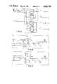
- FIG. 1A typical two-phase, symmetric, nonoverlapped clock generator is shown in FIG. 1.
- the clock input (10)is provided to a level shifter and clock buffer (12).
- the output (14) of the bufferis provided to a divide-by-two circuit (16), which divides the frequency of clock (10) down to a positive-going clock level (18), and a negative-going clock level (20).
- These clock levelsare input to a clock driver waveshaper and buffer (22) that generates the PH1 and PH2 clock lines (24, 26) and the inversions of these lines PH1I and PH2I (28, 30) from the clock levels (18, 20).
- This method of generating two symmetric non-overlapping clocksis preferable to having users externally supply to the chip the two non-overlapping to be buffered or used by the chip directly. This is because it is very difficult to generate symmetric, non-overlapping clocks externally. Board impedance, board signal routing, and clock-chip driving variability combine to make externally generated non-overlapping clocks not very cost effective.
- the prior art circuit of FIG. 1has a major disadvantage.
- a large clock skew, that is clock delay, from the transistion of the external clock input (10) to the generated transistions of the internal PH1 and PH2 clocks (66, 68)occurs due to the buffering and intermediate logic, notably the divide-by-two circuit that is in the critical path to generating PH1 and PH2.
- This clock delay between the internally generated clock and the external system clockmakes it difficult to synchronize logic chip outputs that are activated by using the internal PH1, PH2 clocks, with the external system clock.
- An external timing sourceprovides input waveforms of signal voltage transitions which occur at a first frequency, which is twice the frequency desired by the internal clock.
- a divider circuitdivides the input waveforms into a pair of intermediate waveforms.
- the intermediate waveformshave signal-voltage transistions of opposing polarity which occur at a second frequency that is one-half of the first frequency.
- the input waveform and the intermediate waveformsare supplied to a driver circuit.
- the driver circuitutilizes the intermediate waveforms occurring at the divided-down frequency and the input waveform occurring at the system clock frequency to produce a pair of final waveforms.
- the final waveformshave signal voltage transitions of opposing polarity occurring at the divided-down frequency, but triggerred by and in synchronism with the input waveform occurring at the external clock frequency.
- This clock generatorhas the advantage of removing the divide-by-two circuit from the speed critical path by utilizing the system-clock input directly to synchronize the final clock output.
- FIG. 1is a schematic diagram of a prior art clock generator
- FIG. 2is a schematic diagram of a clock generator in which the present invention is embodied
- FIG. 3is a more detailed schematic diagram of the level shifter and clock buffer (42) and the divide by two circuit (48) shown in FIG. 2;
- FIG. 4is a more detailed logic diagram of the level shifter (76) and reset circuit (80) shown in FIG. 2;
- FIG. 5is a more detailed logic diagram of the clock buffer, driver, wave shaper and buffer (64) of FIG. 2;
- FIG. 6is a more detailed logic diagram of blocks (71, 73) of FIG. 5;
- FIG. 7is a more detailed logic diagram of blocks (74, 76) of FIG. 5;
- FIG. 8is a timing diagram of the clock generator shown in FIGS. 2 and 3.
- PHNn internal unique clock waveforms. Further, let [PH (n+1) modulo n] be defined as the next successive phase initiation time that is asserted after deassertion of PHN. Then, all PHN on a single chip are considered to be symmetric if, and only if, the following three conditions hold within reasonable engineering tolerances, less than 10%:
- Nonoverlap time(the time between deassertion of each PHN and the assertion of the next closest phase in time [PH (n+1) modulo n], must be equal between each successive phase.
- FIG. 2A simplified block diagram of a clock generator in which the present invention is embodied is shown in FIG. 2.
- An external system-clock input (40)which operates at twice the desired frequency of the clock, is supplied to level shifter and clock buffer (42). This produces a pair of input waveforms (44, 46), which are supplied to the divide-by-two circuit (48).
- the divide-by-two circuit (48)divides the input waveforms (44, 46) into a pair of intermediate waveforms (60, 62) of signal-voltage transitions of opposing polarity occurring at a second frequency that is one-half of the input frequency. These intermediate waveforms are supplied to the clock driver waveshaper and buffer (64).
- the clockdriver (64)utilizes the intermediate waveforms occurring at the divided-down frequency and the input waveform occurring at the system-clock frequency to produce a pair of final waveforms (66, 68) of signal-voltage transitions of opposing polarity occurring at the divided-down frequency, the PH2 and PH1 clocks.
- the level shifter and buffer (76) and the reset circuit (80)are shown in more detail in FIG. 4.
- the clock driver waveshaper and buffer (64)is shown in more detail in FIG. 5.
- the PH1 and PH2 clock linesare derived from identical circuits (71, 73), Shown in detail in FIG. 6, which each receive the PH output from the other circuit as the DELIN input.
- the inversions of PH1 and PH2are generated by identical circuits (74, 76), shown in detail in FIG. 7 which are also cross-coupled.
- the waveshapes labeled A, B, C, and Drefer to the nodes which are similarly labeled in FIG. 6.
- the CLK waveshapeis provided by an external clock input which is twice the frequency of the PH1 and PH2 outputs.
- the CLK signal supplied to the divide-by-two circuit (48)results in intermediate waveforms (60, 62), which are labeled DRIV and DRIVB. DRIV and DRIVB change level at each negative-going transition of CLK.
- Node Ais dependent upon the CLK line and switches from a high to low when the CLK line rises. Node A does not depend on the divided-down signal. DRIV, changing level. As Node A switches from high to low, it causes Node D to switch from low to high through the transistor M 1 . Node D, going high, causes the PH1 output to go negative. Node A returns to a high when CLK goes low. It stays high until it is used to trigger the next PH1 falling transition.
- Node Bwill stay high until both the CLK and DRIVB are high, then Node B will switch to low. This sets up Node C to go high upon the condition that DELIN (the PH2 output from Block 73) goes low. The PH2 output will go low in the same way that PH1 went low as companion block (73) has its own nodes A, B, C, and D. Node C going high will cause Node D to go low, which in turn causes PH1 to go high. This chain of events ensures the non-overlapping condition of PH1 and PH2.
- the invertor I2can only source about one milliamp of current, short-circuited, whereas the transistors M 1 and M 2 can supply about 100 milliamps of current. So, if either one of M 1 or M 2 turns on, it will overpower the influence of the invertors I 1 and I 2 on the state of Node D. Once M 1 and M 2 turn off, the I 2 invertor will be stronger than the leakage currents on M 1 and M 2 , so I 2 will be able to hold the state of Node D, whatever that state may be.
Landscapes
- Physics & Mathematics (AREA)
- Nonlinear Science (AREA)
- Manipulation Of Pulses (AREA)
Abstract
Description
This invention relates to integrated logic circuits, and more particularly, to a pipelined, symmetric, two-phase non-overlapping clock generator.
CMOS/NMOS-clocked chip designs use two or more symmetric non-overlapping clock phases to perform a given logic function. This type of clock is used in the Intel 80286 and 80386 microprocessors. Four clocks, PH1, PH1I, PH2, PH2I are distributed in the chip. PH1 and PH2 are traditional NMOS nonoverlapping clocks with equal duty cycles. PH1I and PH2I are the PMOS analogs to PH1 and PH2 and are exactly inversions of PH1 and PH2, respectively. Successive PH1 and PH2 assertions form a microcycle that is 62.5 nanoseconds when the chip is operated at 16-MHz frequency.
In the prior art, the method of generating two nonoverlapped clocks is for the user system to provide an input clock frequency that is exactly twice the frequency of the desired internal clock frequency. Thus, to generate an internal PH1 and PH2 clock frequency of 20 MHz, a 40-MHz-external-clock frequency is applied as input to the chip. This input frequency is then divided by a factor of two to generate a 20-MHz, 50% duty-cycle clock that is used as an input to a waveshaping circuit which generates two symmetric nonoverlapping clocks.
A typical two-phase, symmetric, nonoverlapped clock generator is shown in FIG. 1. The clock input (10) is provided to a level shifter and clock buffer (12). The output (14) of the buffer is provided to a divide-by-two circuit (16), which divides the frequency of clock (10) down to a positive-going clock level (18), and a negative-going clock level (20). These clock levels are input to a clock driver waveshaper and buffer (22) that generates the PH1 and PH2 clock lines (24, 26) and the inversions of these lines PH1I and PH2I (28, 30) from the clock levels (18, 20).
This method of generating two symmetric non-overlapping clocks is preferable to having users externally supply to the chip the two non-overlapping to be buffered or used by the chip directly. This is because it is very difficult to generate symmetric, non-overlapping clocks externally. Board impedance, board signal routing, and clock-chip driving variability combine to make externally generated non-overlapping clocks not very cost effective.
The prior art circuit of FIG. 1 has a major disadvantage. A large clock skew, that is clock delay, from the transistion of the external clock input (10) to the generated transistions of the internal PH1 and PH2 clocks (66, 68) occurs due to the buffering and intermediate logic, notably the divide-by-two circuit that is in the critical path to generating PH1 and PH2. This clock delay between the internally generated clock and the external system clock makes it difficult to synchronize logic chip outputs that are activated by using the internal PH1, PH2 clocks, with the external system clock.
It is an object of the present invention to provide an improved symmetric, non-overlapping clock generator that minimizes the time delay between the external system clock and the internally generated clock signals.
The above object is accomplished in accordance with the invention as follows. An external timing source provides input waveforms of signal voltage transitions which occur at a first frequency, which is twice the frequency desired by the internal clock. A divider circuit divides the input waveforms into a pair of intermediate waveforms. The intermediate waveforms have signal-voltage transistions of opposing polarity which occur at a second frequency that is one-half of the first frequency.
The input waveform and the intermediate waveforms are supplied to a driver circuit. The driver circuit utilizes the intermediate waveforms occurring at the divided-down frequency and the input waveform occurring at the system clock frequency to produce a pair of final waveforms. The final waveforms have signal voltage transitions of opposing polarity occurring at the divided-down frequency, but triggerred by and in synchronism with the input waveform occurring at the external clock frequency.
This clock generator has the advantage of removing the divide-by-two circuit from the speed critical path by utilizing the system-clock input directly to synchronize the final clock output.
The foregoing and other objects, features, and advantages of the invention will be apparent from the following detailed description of a preferred embodiment of the invention as illustrated in the accompanying drawings wherein:
FIG. 1 is a schematic diagram of a prior art clock generator;
FIG. 2 is a schematic diagram of a clock generator in which the present invention is embodied;
FIG. 3 is a more detailed schematic diagram of the level shifter and clock buffer (42) and the divide by two circuit (48) shown in FIG. 2;
FIG. 4 is a more detailed logic diagram of the level shifter (76) and reset circuit (80) shown in FIG. 2;
FIG. 5 is a more detailed logic diagram of the clock buffer, driver, wave shaper and buffer (64) of FIG. 2; and
FIG. 6 is a more detailed logic diagram of blocks (71, 73) of FIG. 5; and
FIG. 7 is a more detailed logic diagram of blocks (74, 76) of FIG. 5; and
FIG. 8 is a timing diagram of the clock generator shown in FIGS. 2 and 3.
Symmetric, non-overlapping clock waveforms are defined as follows.
Let PHN represent n internal unique clock waveforms. Further, let [PH (n+1) modulo n] be defined as the next successive phase initiation time that is asserted after deassertion of PHN. Then, all PHN on a single chip are considered to be symmetric if, and only if, the following three conditions hold within reasonable engineering tolerances, less than 10%:
1. No two PHN can simultaneously be at nonzero volts.
2. All PHN must be asserted (5 volts for current NMOS type of phases) for equal duration within all clock cycles.
3. Nonoverlap time (the time between deassertion of each PHN and the assertion of the next closest phase in time [PH (n+1) modulo n], must be equal between each successive phase.
A simplified block diagram of a clock generator in which the present invention is embodied is shown in FIG. 2. An external system-clock input (40), which operates at twice the desired frequency of the clock, is supplied to level shifter and clock buffer (42). This produces a pair of input waveforms (44, 46), which are supplied to the divide-by-two circuit (48). The input waveshaper and buffer (64).
The divide-by-two circuit (48) divides the input waveforms (44, 46) into a pair of intermediate waveforms (60, 62) of signal-voltage transitions of opposing polarity occurring at a second frequency that is one-half of the input frequency. These intermediate waveforms are supplied to the clock driver waveshaper and buffer (64). The clockdriver (64) utilizes the intermediate waveforms occurring at the divided-down frequency and the input waveform occurring at the system-clock frequency to produce a pair of final waveforms (66, 68) of signal-voltage transitions of opposing polarity occurring at the divided-down frequency, the PH2 and PH1 clocks. These final waveforms are, however, synchronized and triggered by the input waveforms (44, 46) occurring at the input frequency. This circuit effectively removes the divide-by-two circuit (48) from the critical path and passes the input clock directly into the clock driver waveshaping andbuffer circuitry 64 to synchronize the PH1 and PH2 output clocks.
The detailed logic within the blocks (42, 48) shown in FIG. 2 is shown in more detail in FIG. 3.
The level shifter and buffer (76) and the reset circuit (80) are shown in more detail in FIG. 4.
The clock driver waveshaper and buffer (64) is shown in more detail in FIG. 5.
Referring now to FIG. 5, the PH1 and PH2 clock lines are derived from identical circuits (71, 73), Shown in detail in FIG. 6, which each receive the PH output from the other circuit as the DELIN input. The inversions of PH1 and PH2 are generated by identical circuits (74, 76), shown in detail in FIG. 7 which are also cross-coupled.
The circuit of FIG. 6 will now be described with reference to the timing diagram shown in FIG. 8. In FIG. 8, the waveshapes labeled A, B, C, and D refer to the nodes which are similarly labeled in FIG. 6. The CLK waveshape is provided by an external clock input which is twice the frequency of the PH1 and PH2 outputs. The CLK signal supplied to the divide-by-two circuit (48) results in intermediate waveforms (60, 62), which are labeled DRIV and DRIVB. DRIV and DRIVB change level at each negative-going transition of CLK.
Node A is dependent upon the CLK line and switches from a high to low when the CLK line rises. Node A does not depend on the divided-down signal. DRIV, changing level. As Node A switches from high to low, it causes Node D to switch from low to high through the transistor M1. Node D, going high, causes the PH1 output to go negative. Node A returns to a high when CLK goes low. It stays high until it is used to trigger the next PH1 falling transition.
Node B will stay high until both the CLK and DRIVB are high, then Node B will switch to low. This sets up Node C to go high upon the condition that DELIN (the PH2 output from Block 73) goes low. The PH2 output will go low in the same way that PH1 went low as companion block (73) has its own nodes A, B, C, and D. Node C going high will cause Node D to go low, which in turn causes PH1 to go high. This chain of events ensures the non-overlapping condition of PH1 and PH2.
In FIG. 6, the invertor I2 can only source about one milliamp of current, short-circuited, whereas the transistors M1 and M2 can supply about 100 milliamps of current. So, if either one of M1 or M2 turns on, it will overpower the influence of the invertors I1 and I2 on the state of Node D. Once M1 and M2 turn off, the I2 invertor will be stronger than the leakage currents on M1 and M2, so I2 will be able to hold the state of Node D, whatever that state may be. For example, if M1 drives Node D to a high state by overriding the influence of I2, and then when M1 is turned off, leaving Node D in a high impedance state, then invertor I2 will be sympathetic to the high state of Node D. Now, when M1 is turned off, I2 continues to drive a high onto Node D. Leakage current through M1 is not enough to override the influence of invertor I2. If there were no leakages in the transistors M1 and M2, the invertors I1 and I2 would not be necessary.
While the invention has been particularly shown and described with reference to preferred embodiments thereof, it will be understood by those skilled in the art that the foregoing and other changes in form and detail may be made therein without departing from the scope of the invention.
Claims (1)
1. A clock signal generator comprising:
a clock buffer for providing a first input waveform of first signal voltage transitions occurring at a first frequency and a second input waveform of second signal voltage transitions of polarity opposite to the polarity of said first signal voltage transitions, said second signal voltage transitions occurring at said first frequency;
frequency divider means connected to said buffer;
said frequency divider means including first means for dividing said first waveform into a first intermediate waveform of second signal voltage transitions occurring at a second frequency which is a fraction of said first frequency and second means for dividing said second waveform into a second intermediate waveform of second signal voltage transitions occurring at said second frequency and,
driver means connected to said clock buffer and to said frequency divider means,
said driver means including first circuit means and second circuit means for utilizing said first and second intermediate waveforms occurring at said second frequency and said first and second input waveforms occurring at said first frequency to produce a pair of final waveform outputs of signal voltage transitions of opposing polarity occurring at said second frequency.
said first circuit means receiving as an input one of said final waveform output, said first circuit means further including means responsive to other said final waveform outputs (68) for causing said output to change to one level upon the condition that said DELIN input goes to the opposite level,
said second circuit means receiving as an input other said final waveform outputs, said second circuit means further including means responsive to one of said final waveform outputs for causing said output to change to one level upon the condition that said DELIN output goes to the opposite level, thereby ensuring that said final waveforms do not overlap one another,
each of said first and second circuit means further including means responsive to said input waveform for synchronizing said final waveforms with said first and second signal voltage transitions occurring at said first frequency.
Priority Applications (1)
| Application Number | Priority Date | Filing Date | Title |
|---|---|---|---|
| US07/133,325US4816700A (en) | 1987-12-16 | 1987-12-16 | Two-phase non-overlapping clock generator |
Applications Claiming Priority (1)
| Application Number | Priority Date | Filing Date | Title |
|---|---|---|---|
| US07/133,325US4816700A (en) | 1987-12-16 | 1987-12-16 | Two-phase non-overlapping clock generator |
Publications (1)
| Publication Number | Publication Date |
|---|---|
| US4816700Atrue US4816700A (en) | 1989-03-28 |
Family
ID=22458054
Family Applications (1)
| Application Number | Title | Priority Date | Filing Date |
|---|---|---|---|
| US07/133,325Expired - LifetimeUS4816700A (en) | 1987-12-16 | 1987-12-16 | Two-phase non-overlapping clock generator |
Country Status (1)
| Country | Link |
|---|---|
| US (1) | US4816700A (en) |
Cited By (38)
| Publication number | Priority date | Publication date | Assignee | Title |
|---|---|---|---|---|
| US4929854A (en)* | 1988-04-15 | 1990-05-29 | Fujitsu Limited | Clock circuit having a clocked output buffer |
| US4958085A (en)* | 1987-10-30 | 1990-09-18 | Canon Kabushiki Kaisha | Scanning circuit outputting scanning pulse signals of two or more phases |
| US5032740A (en)* | 1989-11-06 | 1991-07-16 | Eastman Kodak Company | Voltage level conversion of a clock signal |
| US5079440A (en)* | 1990-03-15 | 1992-01-07 | Intel Corporation | Apparatus for generating computer clock pulses |
| US5111063A (en)* | 1989-02-03 | 1992-05-05 | Nec Corporation | Integrated clock driver circuit |
| US5155391A (en)* | 1990-10-22 | 1992-10-13 | National Semiconductor Corporation | Synchronous internal clock distribution |
| US5160859A (en)* | 1990-10-22 | 1992-11-03 | National Semiconductor Corporation | Synchronous internal clock distribution |
| US5313605A (en)* | 1990-12-20 | 1994-05-17 | Intel Corporation | High bandwith output hierarchical memory store including a cache, fetch buffer and ROM |
| US5341031A (en)* | 1990-08-27 | 1994-08-23 | Mitsubishi Denki Kabushiki Kaisha | Stable high speed clock generator |
| EP0656688A1 (en)* | 1993-12-03 | 1995-06-07 | Nec Corporation | Clock generating circuit generating a plurality of non-overlapping clock signals |
| US5444407A (en)* | 1992-12-28 | 1995-08-22 | Advanced Micro Devices, Inc. | Microprocessor with distributed clock generators |
| US5444406A (en)* | 1993-02-08 | 1995-08-22 | Advanced Micro Devices, Inc. | Self-adjusting variable drive strength buffer circuit and method for controlling the drive strength of a buffer circuit |
| US5453707A (en)* | 1993-01-13 | 1995-09-26 | Nec Corporation | Polyphase clock generation circuit |
| US5537570A (en)* | 1993-10-12 | 1996-07-16 | Texas Instruments Incorporated | Cache with a tag duplicate fault avoidance system and method |
| US5561792A (en)* | 1992-12-28 | 1996-10-01 | Advanced Micro Devices, Inc. | Microprocessor with software switchable clock speed and drive strength |
| US5623222A (en)* | 1992-09-02 | 1997-04-22 | Nec Corporation | Voltage converting circuit and multiphase clock generating circuit used for driving the same |
| US5638542A (en)* | 1993-12-29 | 1997-06-10 | Intel Corporation | Low power non-overlap two phase complementary clock unit using synchronous delay line |
| US5706484A (en)* | 1995-12-20 | 1998-01-06 | Intel Corporation | Method for eliminating transition direction sensitive timing skews in a source synchronous design |
| US5723995A (en)* | 1995-12-20 | 1998-03-03 | Intel Corporation | Method for eliminating process variation timing skews in a source synchronous design |
| US5726596A (en)* | 1996-03-01 | 1998-03-10 | Hewlett-Packard Company | High-performance, low-skew clocking scheme for single-phase, high-frequency global VLSI processor |
| US5742832A (en)* | 1996-02-09 | 1998-04-21 | Advanced Micro Devices | Computer system with programmable driver output's strengths responsive to control signal matching preassigned address range |
| US5774001A (en)* | 1995-12-20 | 1998-06-30 | Intel Corporation | Method for eliminating multiple output switching timing skews in a source synchronous design |
| US5813028A (en)* | 1993-10-12 | 1998-09-22 | Texas Instruments Incorporated | Cache read miss request invalidation prevention method |
| US5835934A (en)* | 1993-10-12 | 1998-11-10 | Texas Instruments Incorporated | Method and apparatus of low power cache operation with a tag hit enablement |
| US5877656A (en)* | 1995-10-30 | 1999-03-02 | Cypress Semiconductor Corp. | Programmable clock generator |
| US5952863A (en)* | 1996-12-09 | 1999-09-14 | Texas Instruments Incorporated | Circuit and method for generating non-overlapping clock signals for an integrated circuit |
| US6188255B1 (en) | 1998-09-28 | 2001-02-13 | Cypress Semiconductor Corp. | Configurable clock generator |
| US6249157B1 (en)* | 1999-02-02 | 2001-06-19 | Mitsubishi Denki Kabushiki Kaisha | Synchronous frequency dividing circuit |
| US6275086B1 (en)* | 1998-11-19 | 2001-08-14 | Fujitsu Limited | Clock signal generator for an integrated circuit |
| US20030122630A1 (en)* | 1997-02-05 | 2003-07-03 | Fox Enterprises, Inc., A Florida Corporation | Programmable oscillator circuit |
| US20040239433A1 (en)* | 1997-02-05 | 2004-12-02 | Fox Enterprises, Inc. | Worldwide marketing logistics network including strategically located centers for frequency programming crystal oscillators to customer specification |
| US20060103481A1 (en)* | 2004-11-12 | 2006-05-18 | Hon Hai Precision Industry Co., Ltd. | Clock signal generator |
| US20060148035A1 (en)* | 2000-06-28 | 2006-07-06 | Glycofi, Inc. | Methods for producing modified glycoproteins |
| US20060225010A1 (en)* | 2005-03-30 | 2006-10-05 | Nec Electronics Corporation | Semiconductor device and scan test method |
| US20060256906A1 (en)* | 2005-05-13 | 2006-11-16 | Mikhail Itskovich | Discrete-time analog, digitally programmable filter and method |
| US20080224743A1 (en)* | 2006-09-19 | 2008-09-18 | Jungwook Yang | Sequence independent non-overlapping digital signal generator with programmable delay |
| US20100240323A1 (en)* | 2009-03-19 | 2010-09-23 | Qualcomm Incorporated | Frequency divider with synchronized outputs |
| US8073042B1 (en) | 2005-04-13 | 2011-12-06 | Cypress Semiconductor Corporation | Recursive range controller |
Citations (5)
| Publication number | Priority date | Publication date | Assignee | Title |
|---|---|---|---|---|
| US3596188A (en)* | 1969-12-03 | 1971-07-27 | Control Data Corp | Four-phase digital clock |
| US3961269A (en)* | 1975-05-22 | 1976-06-01 | Teletype Corporation | Multiple phase clock generator |
| US4417158A (en)* | 1980-11-20 | 1983-11-22 | Fujitsu Limited | Clock generator circuit |
| US4587441A (en)* | 1982-10-22 | 1986-05-06 | Sgs-Ates Componenti Elettronici S.P.A. | Interface circuit for signal generators with two non-overlapping phases |
| US4686386A (en)* | 1984-03-21 | 1987-08-11 | Oki Electric Industry Co., Ltd. | Power-down circuits for dynamic MOS integrated circuits |
- 1987
- 1987-12-16USUS07/133,325patent/US4816700A/ennot_activeExpired - Lifetime
Patent Citations (5)
| Publication number | Priority date | Publication date | Assignee | Title |
|---|---|---|---|---|
| US3596188A (en)* | 1969-12-03 | 1971-07-27 | Control Data Corp | Four-phase digital clock |
| US3961269A (en)* | 1975-05-22 | 1976-06-01 | Teletype Corporation | Multiple phase clock generator |
| US4417158A (en)* | 1980-11-20 | 1983-11-22 | Fujitsu Limited | Clock generator circuit |
| US4587441A (en)* | 1982-10-22 | 1986-05-06 | Sgs-Ates Componenti Elettronici S.P.A. | Interface circuit for signal generators with two non-overlapping phases |
| US4686386A (en)* | 1984-03-21 | 1987-08-11 | Oki Electric Industry Co., Ltd. | Power-down circuits for dynamic MOS integrated circuits |
Cited By (52)
| Publication number | Priority date | Publication date | Assignee | Title |
|---|---|---|---|---|
| US4958085A (en)* | 1987-10-30 | 1990-09-18 | Canon Kabushiki Kaisha | Scanning circuit outputting scanning pulse signals of two or more phases |
| US4929854A (en)* | 1988-04-15 | 1990-05-29 | Fujitsu Limited | Clock circuit having a clocked output buffer |
| US5111063A (en)* | 1989-02-03 | 1992-05-05 | Nec Corporation | Integrated clock driver circuit |
| US5032740A (en)* | 1989-11-06 | 1991-07-16 | Eastman Kodak Company | Voltage level conversion of a clock signal |
| US5079440A (en)* | 1990-03-15 | 1992-01-07 | Intel Corporation | Apparatus for generating computer clock pulses |
| US5341031A (en)* | 1990-08-27 | 1994-08-23 | Mitsubishi Denki Kabushiki Kaisha | Stable high speed clock generator |
| US5155391A (en)* | 1990-10-22 | 1992-10-13 | National Semiconductor Corporation | Synchronous internal clock distribution |
| US5160859A (en)* | 1990-10-22 | 1992-11-03 | National Semiconductor Corporation | Synchronous internal clock distribution |
| US5313605A (en)* | 1990-12-20 | 1994-05-17 | Intel Corporation | High bandwith output hierarchical memory store including a cache, fetch buffer and ROM |
| US5623222A (en)* | 1992-09-02 | 1997-04-22 | Nec Corporation | Voltage converting circuit and multiphase clock generating circuit used for driving the same |
| EP0822478A3 (en)* | 1992-09-02 | 1998-12-30 | Nec Corporation | Voltage converting circuit and multiphase clock generating circuit for driving the same |
| US5444407A (en)* | 1992-12-28 | 1995-08-22 | Advanced Micro Devices, Inc. | Microprocessor with distributed clock generators |
| US5561792A (en)* | 1992-12-28 | 1996-10-01 | Advanced Micro Devices, Inc. | Microprocessor with software switchable clock speed and drive strength |
| US5453707A (en)* | 1993-01-13 | 1995-09-26 | Nec Corporation | Polyphase clock generation circuit |
| US5444406A (en)* | 1993-02-08 | 1995-08-22 | Advanced Micro Devices, Inc. | Self-adjusting variable drive strength buffer circuit and method for controlling the drive strength of a buffer circuit |
| US5537570A (en)* | 1993-10-12 | 1996-07-16 | Texas Instruments Incorporated | Cache with a tag duplicate fault avoidance system and method |
| US5813028A (en)* | 1993-10-12 | 1998-09-22 | Texas Instruments Incorporated | Cache read miss request invalidation prevention method |
| US5835934A (en)* | 1993-10-12 | 1998-11-10 | Texas Instruments Incorporated | Method and apparatus of low power cache operation with a tag hit enablement |
| US5532633A (en)* | 1993-12-03 | 1996-07-02 | Nec Corporaton | Clock generating circuit generating a plurality of non-overlapping clock signals |
| EP0656688A1 (en)* | 1993-12-03 | 1995-06-07 | Nec Corporation | Clock generating circuit generating a plurality of non-overlapping clock signals |
| US5638542A (en)* | 1993-12-29 | 1997-06-10 | Intel Corporation | Low power non-overlap two phase complementary clock unit using synchronous delay line |
| US5877656A (en)* | 1995-10-30 | 1999-03-02 | Cypress Semiconductor Corp. | Programmable clock generator |
| US6433645B1 (en) | 1995-10-30 | 2002-08-13 | Cypress Semiconductor Corp. | Programmable clock generator |
| US5774001A (en)* | 1995-12-20 | 1998-06-30 | Intel Corporation | Method for eliminating multiple output switching timing skews in a source synchronous design |
| US5723995A (en)* | 1995-12-20 | 1998-03-03 | Intel Corporation | Method for eliminating process variation timing skews in a source synchronous design |
| US5706484A (en)* | 1995-12-20 | 1998-01-06 | Intel Corporation | Method for eliminating transition direction sensitive timing skews in a source synchronous design |
| US5742832A (en)* | 1996-02-09 | 1998-04-21 | Advanced Micro Devices | Computer system with programmable driver output's strengths responsive to control signal matching preassigned address range |
| US5726596A (en)* | 1996-03-01 | 1998-03-10 | Hewlett-Packard Company | High-performance, low-skew clocking scheme for single-phase, high-frequency global VLSI processor |
| US5952863A (en)* | 1996-12-09 | 1999-09-14 | Texas Instruments Incorporated | Circuit and method for generating non-overlapping clock signals for an integrated circuit |
| US20030122630A1 (en)* | 1997-02-05 | 2003-07-03 | Fox Enterprises, Inc., A Florida Corporation | Programmable oscillator circuit |
| US6965272B2 (en) | 1997-02-05 | 2005-11-15 | Fox Enterprises, Inc. | Worldwide marketing logistics network including strategically located centers for frequency programming crystal oscillators to customer specification |
| US6664860B2 (en) | 1997-02-05 | 2003-12-16 | Fox Enterprises, Inc. | Programmable oscillator circuit and method |
| US20040239433A1 (en)* | 1997-02-05 | 2004-12-02 | Fox Enterprises, Inc. | Worldwide marketing logistics network including strategically located centers for frequency programming crystal oscillators to customer specification |
| US6954113B2 (en) | 1997-02-05 | 2005-10-11 | Fox Electronics, Inc. | Programmable oscillator circuit |
| US6388478B1 (en) | 1998-09-28 | 2002-05-14 | Cypress Semiconductor Corp. | Configurable clock generator |
| US6188255B1 (en) | 1998-09-28 | 2001-02-13 | Cypress Semiconductor Corp. | Configurable clock generator |
| US6275086B1 (en)* | 1998-11-19 | 2001-08-14 | Fujitsu Limited | Clock signal generator for an integrated circuit |
| US6466075B2 (en) | 1998-11-19 | 2002-10-15 | Fujitsu Limited | Clock signal generator for generating signal with differing phase for an integrated circuit |
| US6249157B1 (en)* | 1999-02-02 | 2001-06-19 | Mitsubishi Denki Kabushiki Kaisha | Synchronous frequency dividing circuit |
| US20060148035A1 (en)* | 2000-06-28 | 2006-07-06 | Glycofi, Inc. | Methods for producing modified glycoproteins |
| US7375566B2 (en) | 2004-11-12 | 2008-05-20 | Hong Fu Jin Precision Industry (Shenzhen) Co., Ltd. | Clock signal generator |
| US20060103481A1 (en)* | 2004-11-12 | 2006-05-18 | Hon Hai Precision Industry Co., Ltd. | Clock signal generator |
| US20060225010A1 (en)* | 2005-03-30 | 2006-10-05 | Nec Electronics Corporation | Semiconductor device and scan test method |
| US7752516B2 (en)* | 2005-03-30 | 2010-07-06 | Nec Electronics Corporation | Semiconductor device and scan test method |
| US8073042B1 (en) | 2005-04-13 | 2011-12-06 | Cypress Semiconductor Corporation | Recursive range controller |
| US8526558B1 (en) | 2005-04-13 | 2013-09-03 | Cypress Semiconductor Corporation | Recursive range controller |
| US20060256906A1 (en)* | 2005-05-13 | 2006-11-16 | Mikhail Itskovich | Discrete-time analog, digitally programmable filter and method |
| US7769799B2 (en) | 2005-05-13 | 2010-08-03 | Atmel Corporation | Discrete-time analog, digitally programmable filter and method |
| US7612595B2 (en) | 2006-09-19 | 2009-11-03 | Melexis Tessenderlo Nv | Sequence independent non-overlapping digital signal generator with programmable delay |
| US20080224743A1 (en)* | 2006-09-19 | 2008-09-18 | Jungwook Yang | Sequence independent non-overlapping digital signal generator with programmable delay |
| US20100240323A1 (en)* | 2009-03-19 | 2010-09-23 | Qualcomm Incorporated | Frequency divider with synchronized outputs |
| US8265568B2 (en)* | 2009-03-19 | 2012-09-11 | Qualcomm Incorporated | Frequency divider with synchronized outputs |
Similar Documents
| Publication | Publication Date | Title |
|---|---|---|
| US4816700A (en) | Two-phase non-overlapping clock generator | |
| US6194932B1 (en) | Integrated circuit device | |
| US5687134A (en) | Synchronous semiconductor memory capable of saving a latency with a reduced circuit scale | |
| KR940005007B1 (en) | Phase comparator | |
| US5451911A (en) | Timing generator | |
| US6049236A (en) | Divide-by-one or divide-by-two qualified clock driver with glitch-free transitions between operating frequencies | |
| US4882505A (en) | Fully synchronous half-frequency clock generator | |
| KR19980078161A (en) | Delay Loop Luck Circuit of Semiconductor Memory Devices | |
| JPH0946189A (en) | Clock supply circuit | |
| US3935475A (en) | Two-phase MOS synchronizer | |
| KR960026760A (en) | Pulse Signal Shaping Circuit | |
| JPH07107122A (en) | Digital signal transmission circuit | |
| KR100366137B1 (en) | Internal Clock Signal Generation Method and Device | |
| US6194938B1 (en) | Synchronous integrated clock circuit | |
| US5196743A (en) | Low-power clocking circuits | |
| JP2001203585A (en) | Parallel-serial conversion circuit | |
| US4868511A (en) | Digital sequencing circuit | |
| KR100252770B1 (en) | Ring oscillator | |
| US6753715B2 (en) | System for symmetric pulse generator flip-flop | |
| KR100278271B1 (en) | A clock frequency divider | |
| JP2576657B2 (en) | Timing signal generator | |
| RU2110144C1 (en) | Synchronizing device | |
| EP1618660A1 (en) | Enabling method to prevent glitches in waveform | |
| US5053651A (en) | Deglitched digital mixer circuit | |
| KR100465344B1 (en) | Half period signal generating circuit |
Legal Events
| Date | Code | Title | Description |
|---|---|---|---|
| AS | Assignment | Owner name:INTEL CORPORATION, SANTA CLARA, CALIFORNIA, A CORP Free format text:ASSIGNMENT OF ASSIGNORS INTEREST.;ASSIGNOR:IMEL, MICHAEL T.;REEL/FRAME:004802/0551 Effective date:19871116 Owner name:INTEL CORPORATION, SANTA CLARA, CALIFORNIA, A CORP Free format text:ASSIGNMENT OF ASSIGNORS INTEREST;ASSIGNOR:IMEL, MICHAEL T.;REEL/FRAME:004802/0551 Effective date:19871116 | |
| STCF | Information on status: patent grant | Free format text:PATENTED CASE | |
| CC | Certificate of correction | ||
| REMI | Maintenance fee reminder mailed | ||
| FPAY | Fee payment | Year of fee payment:4 | |
| SULP | Surcharge for late payment | ||
| FEPP | Fee payment procedure | Free format text:PAYOR NUMBER ASSIGNED (ORIGINAL EVENT CODE: ASPN); ENTITY STATUS OF PATENT OWNER: LARGE ENTITY | |
| FPAY | Fee payment | Year of fee payment:8 | |
| FPAY | Fee payment | Year of fee payment:12 |