US4811414A - Methods for digitally noise averaging and illumination equalizing fingerprint images - Google Patents
Methods for digitally noise averaging and illumination equalizing fingerprint imagesDownload PDFInfo
- Publication number
- US4811414A US4811414AUS07/020,331US2033187AUS4811414AUS 4811414 AUS4811414 AUS 4811414AUS 2033187 AUS2033187 AUS 2033187AUS 4811414 AUS4811414 AUS 4811414A
- Authority
- US
- United States
- Prior art keywords
- pixel values
- pvn
- image
- array
- pixel
- Prior art date
- Legal status (The legal status is an assumption and is not a legal conclusion. Google has not performed a legal analysis and makes no representation as to the accuracy of the status listed.)
- Expired - Fee Related
Links
Images


Classifications
- A—HUMAN NECESSITIES
- A61—MEDICAL OR VETERINARY SCIENCE; HYGIENE
- A61B—DIAGNOSIS; SURGERY; IDENTIFICATION
- A61B5/00—Measuring for diagnostic purposes; Identification of persons
- A61B5/117—Identification of persons
- A61B5/1171—Identification of persons based on the shapes or appearances of their bodies or parts thereof
- A61B5/1172—Identification of persons based on the shapes or appearances of their bodies or parts thereof using fingerprinting
- G—PHYSICS
- G06—COMPUTING OR CALCULATING; COUNTING
- G06T—IMAGE DATA PROCESSING OR GENERATION, IN GENERAL
- G06T5/00—Image enhancement or restoration
- G06T5/20—Image enhancement or restoration using local operators
- G—PHYSICS
- G06—COMPUTING OR CALCULATING; COUNTING
- G06T—IMAGE DATA PROCESSING OR GENERATION, IN GENERAL
- G06T5/00—Image enhancement or restoration
- G06T5/90—Dynamic range modification of images or parts thereof
- G06T5/94—Dynamic range modification of images or parts thereof based on local image properties, e.g. for local contrast enhancement
- G—PHYSICS
- G06—COMPUTING OR CALCULATING; COUNTING
- G06V—IMAGE OR VIDEO RECOGNITION OR UNDERSTANDING
- G06V40/00—Recognition of biometric, human-related or animal-related patterns in image or video data
- G06V40/10—Human or animal bodies, e.g. vehicle occupants or pedestrians; Body parts, e.g. hands
- G06V40/12—Fingerprints or palmprints
Definitions
- the present inventionrelates to computer processing of fingerprint images
- Optical fingerprinting systemswhich optically generate fingerprint images are also in use.
- Several such optical fingerprinting systemsare disclosed in the U.S. Pat. Nos. to Becker 3,482,498, McMahon 3,975,711, White 3,200,701, Schiller 4,544,267 and Marcus 4,553,387.
- systems such as thesehave not gained widespread acceptance.
- the Schiller U.S. Pat. No. 4,544,267discloses an apparatus in which a finger pressed against a platen provides a fingerprint object which is scanned by an interrogating beam of collimated light that is linearly displaced across the platen thereby maintaining a constant angle between the interrogating light beam and the plane of the object being scanned.
- the Marcus U.S. Pat. No. 4,553,837discloses finger processing apparatus which includes a cylindrical-segment platen which supports a finger.
- Optical scanning equipmentscans the circumference of the platen in such a manner that the angle of incidence of a light beam on the fingerprint object remains constant.
- the Becker U.S. Pat. No. 3,482,498discloses several embodiments of an optical apparatus for producing a rolled fingerprint image, both of which utilize a prism having a totally reflecting surface.
- the embodiment shown in FIG. 1autilizes a plurality of prisms and light sources, and produces only an approximation of the ball and side ridges.
- the embodiment shown in FIGS. 2 and 3utilize a mechanical system actuated by a rolling finger to move and position a light source.
- the fingerprinting systems disclosed in the Schiller and Marcus patents, and the second embodiment disclosed in the Becker patentmay be capable of optically providing a rolled fingerprint image
- these systemsare less than wholly desirable. Perhaps most important, it is not possible to review the image being captured in real-time to determine whether or not critical information required for classification is being captured. Furthermore, the mechanical aspects of these systems, are relatively complicated. As a result, maintaining focus during the time required to obtain the entire rolled fingerprint image can be difficult.
- the fingerprint image produced by the first embodiment of the invention disclosed in the Becker patentprovides an image in real-time, this image only approximates the rolled fingerprint image.
- Prismssuch as those disclosed in the McMahon U.S. Pat. No. 3,975,711 and the White U.S. Pat. No. 3,200,701 utilize the optical principle of total internal reflection to produce a fingerprint image.
- the "plane" of the fingerprintmust be imaged at an observation angle which is not perpendicular to the plane.
- Vertical scale errors, or distortions of distances on the fingerprint image from their true distances along a Y-axis which is generally parallel to a longitudinal axis of the finger,are therefore inherent.
- Prisms which have grooved finger receiving surfacessuch as those disclosed in the McMahon patent will not provide optimum surface contact between the surface of a finger and therefore its fingerprint, and the prism. Portions of the fingerprint which it may be desired to obtain will therefore be lost. Illumination of the fingerprint through prisms such as that shown in the McMahon patent is often unequal, resulting in an image which has varying intensities throughout its area. Furthermore the contrast between ridges and valleys in the fingerprint image produced by these prisms is generally relatively low.
- the present inventionis a method of operating programmable computing means to enhance fingerprint images.
- a noise average methodinput pixel values of an array of input pixel values characteristic of the fingerprint image are processed to produce a noise averaged array of pixel values characteristic of a noise averaged image.
- An input array of pixel value characteristic of a fingerprint imageis received.
- Noise averaging subarrays of input pixel valuesare selected. Each subarray includes an input pixel value to be noise averaged, and a plurality of input pixel values adjacent the pixel value to be noise averaged.
- Noise averaged pixel valuesare generated as a function of a weighted average of the input pixel values in the noise averaging subarrays.
- the noise averaged pixel valuesare then stored as an array of noise averaged pixel values characteristic of the image.
- an illumination equalizing methodinput pixel values of an array of input pixel values characteristic of a fingerprint image are processed to produce an illumination equalized array of pixel values characteristic of an illumination equalized image.
- An array of input pixel values characteristic of a fingerprint imageis received.
- Equalizing subarrays of input pixel valuesare selected. Each subarray includes an input pixel value to be illumination equalized.
- Subarray average valuesare generated as a function of the pixel values within the equalizing subarrays. The subarray average values are subtracted from the corresponding pixel values being equalized to generate pixel difference values. A predetermined constant is added to the pixel difference values to generate intermediate illumination equalized pixel values.
- intermediate illumination equalized pixel valuesare less than a predetermined minimum pixel value, the corresponding illumination equalized pixel values are set equal to the minimum pixel value. If intermediate illumination pixel values are greater than or equal to the minimum pixel value, and less than or equal to a predetermined maximum pixel value, the corresponding illumination equalized pixel values are set equal to the corresponding intermediate illumination equalized pixel values. If the intermediate illumination equalized pixel values are greater than the maximum pixel value, the corresponding illumination equalized pixel values are set equal to the maximum pixel value.
- FIG. 1illustrates elements of an optical fingerprinting system in accordance with the present invention.
- FIG. 2is a view looking into the top of the optics/processor unit shown in FIG. 1.
- FIG. 3Ais a side view of the optics subsystem shown in FIG. 2, illustrating the optical propagation of fingerprint images from the finger prism to the camera when the slap/image selection optics is positioned at its finger image position.
- FIG. 3Bis a side view of the optics subsystem shown in FIG. 2 illustrating the optical propogation of fingerprint images from the slap prism to the camera when the slap/image selection optics is positioned at its slap image position.
- FIG. 4is a detailed perspective view of the lens trolley shown in FIG. 2.
- FIG. 5is a detailed view of the fastening assembly shown in FIG. 2.
- FIG. 6is a perspective view of an individual finger prism shown in FIG. 2.
- FIG. 7is a sectional view of the finger prism shown in FIG. 6.
- FIG. 8is a rear view of the finger prism shown in FIG. 6.
- FIG. 9is a side view of the finger prism shown in FIG. 6.
- FIG. 10is a top view of the finger prism shown in FIG. 6.
- FIG. 11is a bottom view of the finger prism shown in FIG. 6.
- FIG. 12is a graphic representation of the optical properties of the finger prism shown in FIG. 6, when a finger is not positioned within its groove.
- FIG. 13is a graphic representation of the optical properties of the prism shown in FIG. 6, when a finger is positioned within its groove.
- FIG. 14is a detailed view of a portion of the prism and finger shown in FIG. 13, graphically illustrating the optical properties of the prism in conjunction with a finger positioned thereon.
- FIG. 15is a graphic representation of a finger illustrating various characteristics of a fingerprint thereon.
- FIG. 16is a perspective view of an alternative embodiment of the slap print prism shown in FIG. 2.
- FIG. 17is a side view of the slap print prism shown in FIG. 16.
- FIG. 18is a perspective view of the slap print prism shown in FIG. 2.
- FIG. 19is a side view of the slap print prism shown in FIG. 18.
- FIG. 20is a block diagram representation of the processor subsystem of the optics/processor unit shown in FIG. 1, and illustrating its interconnection to other electrical elements of the fingerprinting system.
- FIG. 21is a graphic representation of an image array of image pixel values generated by the frame digitizer shown in FIG. 20.
- FIG. 22is a graphic representation of a noise averaged array of noise averaged pixel values generated by the processor subsystem shown in FIG. 20.
- FIG. 23is a graphic representation of an illumination equalized array of illumination equalized pixel values generated by the processor subsystem shown in FIG. 20.
- FIG. 24is a graphic representation of the noise averaged array, illustrating a subarray of pixel values utilized by the processor subsystem to generate the illumination equalized array.
- FIG. 25is a graphic representation of a directional filtered array of directional filtered pixel values produced by the processor subsystem shown in FIG. 20.
- FIG. 26is a graphic representation of an illumination equalized array illustrating the regular and offset subarrays utilized by the processor subsystem shown in FIG. 20 to produce the directional filtered array.
- FIG. 27is a detailed graphic representation of an illumination equalized array such as that shown in FIG. 26, illustrating the regular and offset subarrays utilized by the processor subsystem shown in FIG. 20 to produce the directional filtered array.
- FIG. 28is a graphic representation of a fingerprint image showing artifacts or hairs therein.
- FIG. 29is a graphic representation of an unhaired array of unhaired pixel values produced by the processor subsystem shown in FIG. 20.
- FIG. 30is a graphic representation of a directional filtered array illustrating a portion of a fingerprint image having an artifact or hair therein.
- FIG. 31is a graphic representation of a curvature corrected array of curvature corrected pixel values generated by the processor subsystem shown in FIG. 20.
- FIG. 32is a view illustrating a template having a pattern of indicia thereon, and an image of the pattern of indicia when the template is positioned on the finger prism shown in FIG. 6.
- FIG. 33is a qraphic repesentation of a curvature correction table of curvature correction data generated and used by the processor subsystem shown in FIG. 20 to produce the curvature corrected array shown in FIG. 31.
- FIG. 34is a graphic representation of a template image array of template image pixel values generated by the processor subsystem shown in FIG. 20 and representing an image of the pattern of indicia shown in FIG. 32.
- FIG. 35is a graphic representation of a vertically scaled array of vertically scaled pixel values generated by the processor subsystem shown in FIG. 20.
- FIG. 36is a view illustrating a template having a pattern of indicia thereon, and an image of the pattern of indicia when the template is positioned on the slap print prism shown in FIG. 16.
- FIG. 37is a graphic representation of a curvature corrected array generated by the processor subsystem shown in FIG. 20 and representative of the image of the pattern of indicia shown in FIG. 36.
- FIG. 38is a graphic representation of a table of vertical scale correction data generated by the processor subsystem from the curvature corrected array shown in FIG. 37, and used to generate a vertically scaled array.
- FIG. 39is a graphic representation of a horizontally scaled array of horizontally scaled pixel values generated by the processor subsystem shown in FIG. 20.
- FIG. 40is a graphic representation of a table of horizontal scale correction data generated by processor subsystem from the image of the pattern of indicia shown in FIG. 32 and used to produce the vertically scaled array shown in FIG. 39.
- FIG. 41is a graphic representation of a vertically scaled array representative of the image of the pattern of indicia shown in FIG. 32.
- FIG. 42is an illustration of a Main Display menu generated and displayed by the data terminal shown in FIG. 1.
- FIG. 43is a detailed view of the display on the optics/processor unit shown in FIG. 1.
- FIG. 44is a detailed view of the key pad on the optics/processor unit shown in FIG. 1.
- FIG. 45is an illustration of a Demographic/Department Information menu generated and displayed by the data terminal shown in FIG. 1.
- FIG. 46is an illustration of a Processing Choices menu generated and displayed by the data terminal shown in FIG. 1.
- FIG. 47is a graphic representation of a booking or applicant card onto which fingerprint images, department information and demographic information can be printed by the printer shown in FIG. 1.
- fingerprinting system 10in accordance with the present invention is illustrated generally in FIG. 1.
- fingerprinting system 10includes an optics/processor unit 12, video monitor 14, printer 16, and data terminal 6, which includes a keyboard 7 and monitor 8.
- Data terminal 6, monitor 14 and printer 16are interfaced to optics/processor unit 12.
- Fingerprinting system 10is capable of providing printed records of both plain or "slap" prints which are simultaneous impressions of the fingerprints of all fingers of a hand other than the thumb, and individual fingerprints.
- Optics/processor unit 12images the slap print and provides a real-time visual display thereof on monitor 14.
- a key 17A-17D on key pad 19is actuated causing optics/processor unit 12 to "freeze" the image by storing digital data representative thereof.
- This imageis then enhanced when the digital data is processed by optics/processor unit 12 in accordance with image enhancement software. Data representative of the enhanced image is then stored.
- the person to be fingerprintedwill position their finger within groove 102 of an individual finger prism such as 20A.
- Optics/processor unit 12will image the fingerprint, and provide a display thereof on monitor 14. This image can then be "frozen”, and data representative thereof processed by optics/processor unit 12 and stored.
- Demographic data characteristic of the person being fingerprinted and department data (or other relevant information) utilized by the organization doing the fingerprintingcan be entered into system 10 by the operator through keyboard 7. This data, along with the stored fingerprint images, can then be printed at proper locations on a document such as a standard booking or applicant card 15 by printer 16. These procedures are all facilitated by system generated menus and prompts which are displayed on monitor 8 of data terminal 6, as well as by display 13 and illumination of buttons 17A-17D of key pad 19.
- Optics subsystem 22includes slap print prism 18', finger prism trolley 24, first slap image mirror 25, slap/finger image selection optics 26, and a sensor such as video camera 28.
- Slap print prism 18'is mounted in such a manner that its finger-receiving surface 150 is generally level and coplanar with a stepped top panel 32 of unit 12.
- First slap image mirror 25is mounted with respect to slap print prism 18' so as to receive slap fingerprint images projected from image projection surface 156 of the prism, and to reflect these images to slap/finger image selection optics 26.
- Slap print prism 18'is illuminated by means of a light source such as lamp 31 which is positioned adjacent to a light-receiving surface 162 of the prism.
- lamp 31is a sideways oriented U-shaped fluorescent bulb having two legs which are shown in cross section. The two legs of lamp 31 extend across light-receiving surface 162 of prism 18', and are surrounded on a side opposite prism 18' by reflector 32.
- Finger prism trolley 24which is illustrated in greater detail in FIG. 4, includes a base 34 to which a plurality of individual finger prisms 20A-20D are mounted by screws or other suitable fasteners (not shown).
- Base 34includes a track-follower section 36 which is slidably received upon a guide track 37.
- Guide track 37is mounted with respect to a sloping front panel 38 of unit 12 by means of a mounting bracket 39.
- each finger prism 20A-20Dhas an upper surface 100 which includes a finger-receiving groove 102.
- Prisms 20A-20Dare spaced from one another by triangular shaped mirror blocks 40 which have reflective or mirror side surfaces 41 which angle away from side surfaces 112 of prisms 20A-20D and intersect at a point toward slap/finger image selection optics 26.
- End mirror blocks 42are positioned adjacent side surfaces 112 of prisms 20A and 20D which are opposite mirror blocks 40. End mirror blocks 42 also have a reflective side surface 43 which angles away from side surfaces 112 in a direction toward slap/finger selection optics 26.
- Mirror blocks 40have their top surface covered by cover plates 44 (some of which are shown in phantom in FIG. 2) which extend between adjacent prisms 20A-20D.
- Finger prism trolley 24is mounted with respect to unit 12 at an angle in such a manner that finger-receiving grooves 102 of prisms 20A-20D are generally parallel with top panel 50 of the unit.
- a finger-receiving cutout or aperture 51extends through top panel 50 and sloping side panel 38 at a position adjacent trolley 24 to expose groove 102 of one of prisms 20A-20D.
- trolley handle 52which extends through panel 38, an operator can slide trolley 24 along guide track 37 in such a manner as to position groove 102 of a desired finger prism 20A-20D adjacent aperture 51.
- a lamp 53which can be identical to lamp 31 previously described, is mounted with respect to unit 12 below aperture 51 and adjacent a light-receiving surface 104 of whichever prism 20A-20D has been positioned adjacent aperture 51.
- Light from lamp 53will directly enter light-receiving surface 104, and be reflected by surfaces 41 and 43 of mirror blocks 40 and 42, respectively, into side walls 112 of the selected finger prism 20A-20D.
- a fingerprint image of a finger positione- within groove 102 of the selected prism 20A-20Dwill thereby be propagated from image propagation surface 106 toward slap/finger image selection optics 26.
- Slap/finger image selection optics 26includes a mounting plate 60 which has a second slap image mirror 61 and a slap image focusing lens assembly 62, as well as a finger image mirror 63 and finger image focusing lens assembly 64 mounted to a lower side thereof.
- Finger image mirror 63is mounted to mounting plate 60 by means of mounting brackets 65, and is oriented at an angle so as to receive fingerprint images propagated from one of finger prisms 20A-20D and to reflect the fingerprint image to a lens (not separately visible) within finger image focus lens assembly 64.
- Lens assembly 64is mounted to mounting plate 60 by means of mounting bracket 66.
- Second slap image mirror 61is mounted to mounting plate 60 by mounting brackets 67 at a position adjacent finger image mirror 63.
- Mirror 61is oriented at such an angle as to receive slap print images from first slap image mirror 25, and to reflect these images to a lens (not separately visible) within lens assembly 62.
- Lens assembly 62is mounted to mounting plate 60 by means of mounting bracket 68.
- the lenses within lens assemblies 62 and 64can be adjustably positioned along their optical axis to facilitate optical focusing adjustments of subsystem 22.
- a motor mounting bracket 70is mounted to a left side panel 71L of unit 12, while a support bracket 72 is mounted to right side panel 71R.
- Mounted to and extending bbetween brackets 70 and 72is a pair of guide rods 73.
- Guide rods 73are mounted to brackets 70 and 72 by means of fasteners 74 in the embodiment shown.
- Mounting plate 60is slidably suspended from guide rods 73 by means of slide bushings 75A-75C.
- a motor 76 which is interfaced to processor subsystem 30is mounted to a lower face (not visible) of mounting bracket 70, and has a drive shaft 77 which extends through the bracket.
- a drive wheel 78is mounted to shaft 77.
- An idler wheel 79is rotatably mounted to an idler bracket 99.
- Idler bracket 99is mounted acrossguide rods 73.
- FIG. 5A flexible fastening assembly 81 for flexibly fastening belt 80 to mounting plate 60 is illustrated in FIG. 5.
- Fastening assembly 81includes a clamp 82 which has a slot (FIG. 2) into which drive belt 80 is fixedly clamped.
- Clamp 82also has a pair of downward extending arms 83 on its opposite sides. Ends of a flexible member such as stretched spring 84 are fastened to arms 83. A central portion of spring 84 is fastened to mounting plate 60 by means of clamp or bracket 85.
- Motor 76is interfaced to a processor subsystem 30 of optics/processor unit 12. In response to finger prism select signals from processor subsystem 30, motor 76 will rotate in a clockwise direction as viewed in FIG. 2, thereby driving mounting plate 60 (slap/finger image selection optics 26) along guide rods 73 to a rightmost or finger prism select position illustrated in FIGS. 2 and 3A. Mounting plate 60 is driven in this manner until slide bushing 75B is positioned against adjustable stop 86 and actuates microswitch 87. Microswitch 87 is interfaced to processor subsystem 30, and provides signals representative of the positioning of mounting plate 60 to the finger prism select positon.
- finger prism focus lens assembly 64With slap/finger image selection optics 26 in the finger prism select position, video camera 28, finger prism focus lens assembly 64, and finger image mirror 63 are all aligned with the finger prism 20A-20D with has been positioned adjacent aperture 51. Visual images of fingerprints of fingers positioned with groove 102 will thereby be propagated from image propagation surface 106 of the selected prism 20A-20D along finger image optical path 88, reflecte by mirror 63, focused by the lens within assembly 64, and imaged by camera 28.
- motor 76In response to slap print prism select signals from processor subsystem 30, motor 76 will rotate in a counterclockwise direction, thereby pulling mounting plate 60 and slap/finger image selection optics 26 to a slap print select or leftmost position (not shown) when viewed from FIG. 2. Slide bushing 75C will then actuate microswitch 89, which in turn provides slap print positioning select signals to processor subsystem 30. Processor subsystem 30 then stops rotation of motor 76.
- second slap image mirror 61 and slap print focusing lens assembly 62will be aligned about a slap print optical path 90 between slap print prism 18', first slap image mirror 25, and camera 28.
- Slap print images of fingers positioned on slap print prism 18'will thereby be propagated from image propagation surface 156 of the prism along slap print optical path 90, reflected by mirrors 25 and 61, focused by the lens within assembly 62, and imaged by camera 28.
- Video signals representative of fingerprint images imaged by camera 28are provided to processor subsystem 30.
- Key pad 19is illustrated in FIGS. 1, 20, and 44. As perhaps best illustrated in FIG.
- key pad 19is formed by a YES key 17A, a NO key 17B, a CAPTURE key 17C, and an amputee or AMP Key 17D.
- Keys 17A-17Dare preferably fabricated of a translucent material such as plastic, and have a light source such as LEDs 21A-21D, respectively, positioned thereunder. LEDs 21A-21D are each individually interfaced to processor subsystem 30 as shown, and can be individually lit or illuminated by the processor subsystem.
- Display 13is illustrated in greater detail in FIG. 43.
- display 13includes a left hand representation or indicia 312, and a right hand indicia 314.
- Each finger of indicia 312 and 314have a light such as LEDs 316A ⁇ 316E and 318A-318E associated therewith.
- LEDs 316A-316Eare positioned in the thumb, index, middle, ring, and little fingers of left hand indicia 312.
- Leds 318A-318Eare positioned in the thumb, index, middle, ring and little fingers of right hand indicia 314.
- Leds 316A-316E and 318A-318Eare each interfaced (FIG. 20) individually to processor subsystem 30 so as to be capable of individual illumination thereby.
- Prism 20Ais an optical device fabricated of light-propagating material such as plastic which is characterized by an index of refraction.
- prisms 20A-20Dare machined from acrylic polymer, although they can also be molded from this or other materials.
- prism 20Ahas a first or sloping upper surface 100 which has a finger-receiving groove 102 therein, and a front face which includes both a second or light-receiving surface 104 and a third or image propagation surface 106.
- Prism 20Aalso includes a fourth or bottom surface 108, a fifth or back surface 110, and two side faces or surfaces 112.
- Prism 20Ahas a width of dimension D1, and an overall depth of dimension D2.
- Back surface 110is perpendicular to bottom surface 108 and extends to a height of dimension D3 from the bottom surface.
- Upper surface 100intersects back surface 110 at an angle Al with respect to bottom surface 108.
- Light-receiving surface 104extends perpendicularly from bottom surface 108 to a height of dimension D4.
- the magnitude of angle A1will depend upon the index of refraction of the material from which prism 20A is manufactured. In one preferred embodiment in which prism 20A is manufactured of acrylic polymer, angle A1 is 35°.
- dimensions D1-D4are 1.58 inches, 2.35 inches, 1.62 inches, and 0.95 inches, respectively.
- groove 102is elongated and contoured to receive a finger.
- Groove 102includes both a fingerbody portion 113 and a fingertip portion 114.
- Fingerbody portion 113 and fingertip portion 114 of groove 102both include a bottom wall 116 and side walls 118.
- the deepest part of bottom wall 116 of fingerbody portion 113is at a constant depth of dimension D8 with respect to upper surface 100.
- the deepest part of bottom wall 116 of fingertip portion 114slopes from its intersection with fingerbody portion 113 toward upper surface 100 at an angle A5 (45° in one embodiment) with respect to bottom surface 108.
- A545° in one embodiment
- bottom wall 116curves between portions 113 and 114 at a radius of curvature defined by dimension D6.
- dimension D6is a 2.00 inch radius of curvature. This radius of curvature (dimension D6) is centered at a point displaced from the intersection of upper surface 100 and back surface 110 by length of dimension D7.
- dimension D8is 0.50 inches while dimension D7 is 0.72 inches.
- bottom wall 116 of groove 102is semicircular having a radius of curvature characterized by dimension D8. This radius of curvature (dimension D8) can be constant throughout the length of groove 102.
- Side walls 118are preferably planar, and form an angle A2 with respect to side surfaces 112 which are perpendicular to both upper surface 100 and bottom surface 108 of prism 20A. In one preferred embodiment, angle A2 is 221/2°.
- groove 102has been found to permit the highest or optimum degree of contact between a finger (not shown in FIGS. 6-11) and the various surfaces of the groove. This feature is especially important for fingertip portion 114 of groove 102 so that an image of the largest possible area of the fingerprint on the tip of a finger is propagated from prism 20A.
- Dimensions D6, D7 and D8, as well as angle A2will of course vary depending upon the size of the finger to be received by groove 102.
- the size of grooves 102 of each prism 20A-20D on trolley 24is different so that a prism having a properly sized groove 102 can be selected as needed for the particular finger of a particular person being fingerprinted. In general, the larger the finger being fingerprinted, the larger the groove 102 of the selected prism 20A-20D.
- Dimension D1 of prism 20Awill of course also have to increase for prisms 20A-20D with larger grooves 102 (dimension D8).
- image propagation surface 106 and light-receiving surface 104are both curved so as to function as lenses.
- Light-receiving surface 104forms a cylindrical lens and has a radius of curvature defined by dimension D9. This radius of curvature (dimension D9) is centered about a point of dimension D1/2 from side surfaces 112, and spaced from back surface 110 by a distance of dimension D10. In the embodiment of prism 20A described above, dimension D9 is 1.88 inches while dimension D10 is 0.25 inches.
- the radius of curvature or dimension D9 of lensed light-receiving surface 104is therefore perpendicular to back surface 110 and parallel to bottom surface 108.
- light-receiving surface 104can be characterized as being cylindrically curved about an imaginary vertical axis 105 which is perpendicular to bottom surface 108 and parallel to back surface 110.
- Image propagation surface 106is formed as a spherical convex lens in the embodiment shown, and has a radius of curvature of dimension D11 in both horizontal (X) and vertical (Y) directions.
- radius of curvature or dimension D11is centered at a distance of dimension D3 from bottom surface 108, halfway about back surface 110 (d1/2) and a distance of dimension D10 from back surface 110.
- dimension D11is 2.00 inches.
- various surfacesare coated by an opaque substance to inhibit transmission of light.
- bottom surface 108, back surface 110, and planar portions of upper surface 100 other than those of groove 102are coated with an opaque substance.
- portions of side surfaces 112 adjacent back surface 110are also coated. Black paint can be applied to the above-identified surfaces to prevent transmission of light through absorption.
- prism 20A(which are similar to those of prisms 20A-20D) are described with reference to FIGS. 12-14.
- Prism 20Ais designed to utilize the optical principal of frustration of total internal reflection. Due to the relative indexes of refraction of air and the material of which the prism 20A is constructed, and the angles of upper surface 100 and surfaces 116 and 118 of groove 102 with respect to image propagation surface 106 and light-receiving surface 104, all light incident upon groove 102 when a finger is not present thereon is refracted downward toward bottom surface 108 or sideways toward side surfaces 112 upon its entry into prism 20A as illustrated in FIG. 12. Most importantly, virtually none of the light entering groove 102 will be directed out of image propagation surface 106. Virtually all of the light which strikes bottom surface 108 or the opaque portions of side surfaces 112 is absorbed due to the opaque coating, and not re-reflected.
- Light from lamp 53will enter prism 20A through light receiving surface 104, image propagation surface 106, and portions of side faces 112 which are not coated with opaque material. Light so entering which impinges upon groove 102 will either pass through the groove and exit prism 20A, or be internally reflected to one of the opaque surfaces such as bottom surface 108 or back surface 110, and absorbed. Virtually none of the light incident upon prism 20A from lamp 53 will exit image propagation surface 106. As a result, an observer looking into image propagation surface 106 will see only "black" when no finger is positioned on surfaces 116 or 118 of groove 102.
- Fingerprint 134is a pattern formed by ridges 136 (light areas) and valleys 138 (dark areas) of the finger pad.
- portions of prism 20A at which ridges 136 contact a surface such as 116 of groove 102are characterized by a skin-prism material boundary, while those portions at which valleys 138 are adjacent surface 116 are characterized by an air-prism material boundary as if a finger were never positioned in groove 102.
- a visual image of fingerprint 134is propagated through image propagation surface 106.
- This fingerprint imagehas "light” areas corresponding to ridges 136 of the fingerprint 134, and "dark” areas corresponding to valleys 138.
- the fingerprint image of finger 132 propagated from prism 20Awill be distorted from that of a planar "rolled" fingerprint image of the same finger. These distortions are broadly characterized as curvature errors, and size or scale errors, and are caused by different characteristics of finger 132, prism 20A, and their interaction.
- fingers such as 132can be characterized by an imaginary longitudinal axis 139 which extends along the finger.
- the fingerpad on which fingerprint 134 is locatedis a compound curved surface in that it has base curvature about both an X-base curve axis 140 (generally referred to as an X-axis) and a Y-base curve axis 141 (generally referred to as a Y-axis).
- X-base curve axis 140is oriented in a circumferential direction about longitudinal axis 139, and is formed by a locus of points which are perpendicular to a given point about the longitudinal axis.
- Portions of fingerprint 134 about an X-base curve axis such as 140would be colinear in a rolled fingerprint of fingerprint 134.
- the fingerprint image of fingerprint 134 propagated from image propagation surface 106 of prism 20Ais planar, with an imaginary axis 142 which is perpendicular to the image plane (i.e., a plane "parallel" to image propagation surface 106) forming an observation angle OA with respect to longitudinal axis 139 of finger 132.
- Observation angle OAwill be equal to angle A1 (FIG. 7) for those portions of the fingerprint image corresponding to portions of finger 132 which are positioned on fingerbody portion 113 of groove 102.
- Observation angle OAincreases in accordance with the upwardly curved bottom wall 116 for those portions of the fingerprint image corresponding to portions of finger 132 which are positioned on fingertip portion 114 of groove 102.
- portions of fingerprint 134 along an X-base curve axis such as 140will appear as being curved upward in the fingerprint image, as opposed to being colinear if imaged at an observation angle OA of ninety degrees.
- FIG. 32A graphic representation of these curvature errors inherently produced by prism 20A is illustrated in FIG. 32 where an image of a line 254 is curved about an X-base curve axis such as 140 and positioned in groove 102.
- X-base curve axissuch as 140
- the amount of curvature errorchanges for portions of fingerprint 134 at different X-base curve axes such as 140 along Y-base curve axis 141
- the amount of curvature error variation over the relatively small part of finger 132 which is imagedis small. Curvature errors at all points of fingerprint 134 along Y-axis 141 are therefore essentially equal.
- Scale errorsare also caused by the fact that fingerprint 134 is on a compound curved surface of finger 132, and is imaged at an observation angle OA other than ninety degrees with respect to longitudinal axis 139.
- true distances of portions of fingerprint 134 along a given Y-base curve axis such as 141will be distorted.
- two ridges 136which are actually separated about Y-base curve axis 141 on the finger by a given amount will appear to be compressed and separated by a distance less than the given amount.
- this Y-axis scale erroris not constant about Y-base curve axis 141 since observation angle OA increases as bottom surface 116 in fingertip portion 114 of groove 102 curves upward toward surface 100 in the direction of image propagation surface 106.
- X-axis scale errorsare inherent in portions of the fingerprint image which represent portions of the fingerprint about an X-base curve axis such as 140. These X-axis scale errors are also nonlinear due to curvature of fingerprint 134 along its X-base curve axis 140. For example, portions of fingerprint 134 at its center (i.e., opposite the fingernail), and portions on its side, which are separated by a given distance along X-base curve axis 140 will appear to be separated by different distances in the fingerprint image. Distances on the side of finger 132 will be compressed with respect to those in the center of the fingerprint.
- the curved or lensed nature of image propagation surface 106 of prism 20Amagnifies the fingerprint image of fingerprint 134 before it is propagated therefrom. Since groove 102 is actually an elongated and compound curved surface, different portions of the groove, and therefore different portions of fingerprint 134 when finger 132 is placed within the groove, will be at different distances from image propagation surface 106. This factor coupled with well known geometric optic principles results in different portions of fingerprint 134 being magnified to different degrees or amounts. Portions of fingerprint 134 near tip 145 of finger 132 will be nearest surface 106 and magnified the least amount. Portions of fingerprint 134 near back 143 of finger 132 will be positioned furthest from surface 106 and magnified the most. Portions of fingerprint 134 near sides 144 (only one side is visible in FIG. 15) will be magnified by an amount between the amount of those portions at back 143 and tip 145.
- FIGS. 16 and 17A first embodiment of slap print prism 18 is illustrated in FIGS. 16 and 17. Like individual finger prism 20A, slap print prism 18 has a first or finger-receiving surface 150, a second or light-receiving surface 154, a third or image propagation surface 156, a fourth or bottom surface 158, back surface 160, and side surfaces 162. Bottom surface 158 has a depth of dimension D20, and a width of dimension D21. Light-receiving surface 154 and back surface 160 are perpendicular to and have a height of dimensions D22 and D23, respectively, from bottom surface 158. Finger receiving surface 150 is planar, and forms an angle A5 with respect to bottom surface 158.
- Image propagation surface 156is curved to function as a cylindrical lens, and has a radius of curvature of dimension D24 centered about a point at a distance of dimension D25 above the intersection of finger-receiving surface 150 and back surface 160, and a distance of dimension D26 toward light-receiving surface 154 from back surface 160.
- Image propagation surface 156can therefore be characterized as a cylindrical lens having a radius of curvature about an imaginary horizontal axis 151 which is parallel to both back surface 160 and bottom surface 158.
- Dimension D21 of slap print prism 18must be sufficient so as to enable a plurality of fingers (e.g., four fingers of a hand less the thumb) to be positioned on finger-receiving surface 150.
- dimension D21is five inches.
- dimension D20is 1.75 inches
- dimension D22is 1.38 inches
- dimension D23is 1.25 inches
- dimension D24is 1.00 inches
- dimension D25is 0.75
- dimension D26is 0.88 inches.
- Slap print rism 18utilizes and operates on the same optical principles as that of individual fingerprint prism 20A described above.
- Bottom surface 158, side surfaces 162, and back surface 160are coated with black paint so as to make these surfaces opaque.
- Slap print images of the four fingers of a hand, excluding the thumb, which are positioned on finger-receiving surface 150will be propagated through image propagation surface 156.
- Valleys 138 of a fingersuch as 132 (FIG. 15) will be "dark" in the image, while ridges 136 will be light.
- image propagation surface 156causes this surface to function as a lens, and magnifies the image in a direction corresponding to that along the longitudinal axis (i.e., Y-base curve axis) of the finger.
- This magnificationpartially corrects for scale errors along Y-base curve axis 141 (FIG. 15) due to the observation angle OA at which fingerprint 134 is imaged.
- finger-receiving surface 150is planar, fingerprint 134 of a finger such as 132 is forced into a planar orientation when positioned on surface 150.
- X-axis curvature and scale errors in fingerprint images provided by slap print lens 18are negligible compared to those of images provided by finger prisms such as 20A.
- FIGS. 3A, 3B, 18 and 19A second or alternative embodiment of the slap print prism, that being slap print prism 18', is illustrated in FIGS. 3A, 3B, 18 and 19.
- Slap print lens 18'is identical to slap print lens 18 previously described in all respects except for image propagation surface 156' which is coplanar with light-receiving surface 162. Image propagation surface 156' does not, therefore, magnify fingerprint images of fingers such as 132 positioned on finger-receiving surface 150. As a result, Y-axis scaling errors are not partially corrected.
- Slap print lens 18'functions in all other regards exactly like that of slap print lens 18 previously described.
- processor subsystem 30includes programmable computing means such as computer 200, random access memory or RAM 202, read only memory or ROM 204, and frame digitizer 206.
- Fingerprint images from optics subsystem 22are imaged by camera 28 through its objective lens.
- camera 28generates video signals which are representative of the fingerprint image.
- the video signalsare then distributed to both video monitor 14 and frame digitizer 206.
- Video monitor 14(which will typically be interfaced to microprocessor 200 through a video driver which is not shown) can thereby provide a real-time display of the fingerprint image being imaged by camera 28.
- camera 28 and monitor 14are commercially available devices which utilize a standard raster and standard frame rates.
- Computer 200is preferably a commercially available 32-bit microprocessor.
- Frame digitizer 206provides the digital image data in the form of an array of pixel values representative of the intensity of the fingerprint image at corresponding discrete or pixel locations.
- An image array IA of pixel values PVn,m Iis illustrated in FIG. 21.
- Image array IAis formed of N rows and M columns of pixel values PVn,m I .
- image array IAis formed of N equal to four hundred and eighty rows and M equal to five hundred and twelve columns of pixel values PVn,m I .
- Pixel values PVn,m Iare digital values representative of the intensity of the fingerprint image at corresponding pixel locations PLn,m of image array IA.
- frame digitizer 206includes an eight-bit analog-to-digital converter which converts the video signals to eight-bit pixel values PVn,m I characteristic of image intensity at corresponding pixel locations PLn,m.
- an eight-bit pixel value PVn,m I representative of a decimal zeroi.e. "00000000”
- PVMINminimum pixel value
- a pixel value representative of a decimal two hundred and fifty-sixi.e., "11111111”
- a pixel value representative of a decimal two hundred and fifty-sixi.e., "11111111”
- a pixel value representative of a digital 128i.e., "10101010" represents a pixel location PLn,m having an intensity half-way between the lowest and highest intensities(i.e., grey).
- pixel values PVn,m I of image array IAwill be stored within RAM 202 at indexed locations corresponding to pixel locations PLn,m.
- Computer 200will then retrieve image array pixel values PVn,m I and process them in accordance with a Noise Average software algorithm stored in ROM 204 to produce a noise averaged array NAA of pixel values PVn,m N (FIG. 22.
- Noise averaged pixel values PVn,m Nare then temporarily stored within RAM 202 prior to implementation of subsequent image processing software algorithms.
- computer 200generates an illumination equalized array IEA of illumination equalized pixel values PVn,m E in accordance with an Illumination Equalize algorithm, a directional filtered array DFA of directional filtered pixel values PVn,m D in accordance with a Directional Filter algorithm, and an unhaired array UA of unhaired (artifact removed) pixel values PVn,m U in accordance with an Unhair algorithm.
- Unhaired pixel values PVn,m Uare then translated in position in accordance with a Curvature Correction algorithm to generate a curvature corrected array CCA of curvature corrected pixel values PVn,m C .
- Care then scaled or translated in position, first vertically to produce a vertically scaled array VA of vertically scaled pixel values PVn,m V , and then horizontally to produce a horizontally scaled array HA of horizontally scaled pixel values PVn,m H .
- This processingis done in accordance with Vertical Scaling and Horizontal Scaling algorithms, respectively.
- the horizontally scaled array HA of pixel values PVn,m His thresholded to produce a threshold array of thresholded values PVn,m T characteristic of the enhanced fingerprint image.
- the thresholded array of pixel valuesare then stored in RAM 202, and can be utilized by printer 16 to produce a printed record of the fingerprint image.
- computer 200will retrieve pixel values PVn,m I of image array IA (FIG. 21) from RAM 202, and process these pixel values in accordance with a Noise Average program stored within ROM 204. As a result of this processing, computer 200 generates a noise averaged array NAA of noise averaged pixel values PVn,m N as illustrated in FIG. 22.
- the Noise Average programremoves random variations, or noise, in imaged pixel values PVn,m I which can be introduced for various reasons such as electronic or electromagnetic noise.
- Each noise averaged pixel value PVn,m N at pixel locations PLn,m of noise averaged array NAAis computed as a function of weighted average of the particular image pixel value PVn,m I at the same pixel location PLn,m of image array IA, and a plurality of image pixel values PVn,m I at pixel locations PLn,m surrounding or in the area of the particular pixel value PVn,m I being noise averaged.
- noise averaged pixel values PVn,m Nare computed as a function of a weighted average of a given image pixel value PVn,m I , and pixel values PVn,m I at pixel locations PLn,m of image array IA immediately adjacent to the given pixel value.
- a formula for computing noise averaged pixel values PVn,m N in accordance with a preferred weighted average functionis described by Equation 1 below. Other weighted average functions can of course also be used. ##EQU1##
- Equation 1assigns the center pixel value PVn,m I (the particular pixel value to be noise averaged) a weight of four, adjacent side pixel values a weight of two, and adjacent corner pixel values a weight of one.
- Equation 2describes as an example the application of Equation 1 to a particular image pixel value PV2,2 I to be noise averaged. ##EQU2##
- the reasonis that there are no "adjacent" pixel values beyond the edge of image array IA. In one embodiment these "edge" pixel values are ignored by the Noise Average program since they likely represent unimportant portions of the fingerprint image anyway.
- the noise averaged pixel values PVn,m N at these edgesare simply set equal to their corresponding pixel values PVn,m I in the image
- computer 200Having generated a noise averaged array NA of pixel values PVn,m N in accordance with the above-described approach, computer 200 will store the noise averaged pixel values at indexed locations within RAM 202 for subsequent processing.
- illumination equalized pixel values PVn,m Efrom noise averaged pixel values PVn,m N is described with reference to FIG. 24.
- computer 200For a particular pixel value PVn,m N at a particular pixel location PLn,m that it is desired to illumination equalize, computer 200 first selects a subarray SA of pixel values which includes the pixel value to be illumination equalized. Although subarray SA has been chosen as a three-by-three subarray with the particular pixel value PVn,m N to be equalized in the center thereof for purposes of example in FIG. 24, subarrays of a larger size are preferred and can produce better results. In one embodiment, computer 200 selects an eight-by-eight subarray of pixel values surrounding the pixel value to be illumination equalized. However, the algorithm is fully described with the three-by-three subarray SA illustrated in FIG. 24.
- Computer 200then computes the illumination equalized pixel value PVn,m E as a function of the particular noise averaged pixel value PVn,m N to be illumination equalized, the subarray average value SAVn,m for the particular pixel value to be illumination equalized, and a constant K characteristic of an average illumination expected of pixel values of the image.
- Constant K(which can be stored in RAM 202 or ROM 204) is a threshold value and can be set as a function of noise in the fingerprint image.
- computer 200first generates a pixel difference value PDVn,m representative of the difference between the particular pixel value PVn,m N to be illumination equalized, and the subarray average value SAVn,m of the subarray of which it is an element. This operation is mathematically described by Equation 5.
- Constant Kis then added to pixel difference values PVDn,m to generate an intermediate illumination equalized pixel value IEPVn,m as described by Equation 6 below.
- the illumination equalized pixel value PVn,m Eis finally computed as a function of its corresponding intermediate illumination equalized pixel value IEPVn,m. If the intermediate illumination equalized pixel value IEPVn,m is less than the minimum pixel value PVMIN or greater than the maximum pixel value PVMAX, the illumination equalized pixel value PVn,m E is unconditionally set to PVMIN or PVMAX, respectively.
- the illumination equalized pixel value PVn,m Eis set to the intermediate illumination equalized pixel value IEPVn,m if IEPVn,m is greater than or equal to the minimum pixel value PVMIN, and less than or equal to the maximum pixel value PVMAX.
- an entire illumination equalized array IEA of pixel values PVn,m Ecan be generated by computer 200.
- Computer 200will store illumination equalized pixel values PVn,m E in RAM 202 for subsequent processing.
- the fingerprint image characterized by illumination equalized array IEAis formed by pixel values PVn,m E which represent relatively light curves characteristic of fingerprint ridges 136 (FIG. 15), and pixel values which represent relatively dark curves characteristic of fingerprint valleys 138.
- pixel values PVn,m Ewhich represent relatively light curves characteristic of fingerprint ridges 136 (FIG. 15)
- pixel valueswhich represent relatively dark curves characteristic of fingerprint valleys 138.
- This directional filteringis performed by computer 200 in accordance with a Directional Filter program stored within ROM 204.
- the resultis a directional filtered array DFA of directional filtered pixel values PVn,m D as illustrated in FIG. 25.
- the Directional Filtering programis implemented by computer 200 in a multiple-step manner.
- computer 200computes an absolute value of the difference between that particular pixel value and a horizontally adjacent pixel value (HorizDif), a vertically adjacent pixel value (VertDif), an adjacent pixel value at a positive slope (PosDif) and an adjacent pixel value at a negative slope (NegDif). This procedure is described generally by Equations 11-14 below.
- Horizontal difference values HorizDifn,m, vertical difference values VertDifn,m, positive difference values PosDifn,m and negative difference values NegDifn,m for pixel values PVn,m E for each 1 ⁇ n ⁇ N and 1 ⁇ m ⁇ Mare stored at indexed locations within RAM 202.
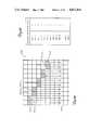
- computer 200next divides illumination equalized array IEA into a plurality of regular subarrays 230A-230Y (illustrated with solid lines) and offset subarrays 232A-232JJ (illustrated with broken lines). Offset subarrays 232A-232JJ are offset both horizontally and vertically with respect to regular subarrays 230A-230Y in the embodiment shown. All pixel values PVn,m E of illumination equalized array IEA will be located within both one of regular subarrays 230A-230Y and one of offset subarrays 232A-232JJ.
- Subarrays 230A-230Y and 232A-232JJare sized so as to have more pixel values PVn,m E on a side than an expected width of a fingerprint ridge 136 (FIG. 15) or valley 138 as represented by the pixel values of the subarray.
- computer 200causes subarrays 230A-230Y and 232A-232JJ to be rectangular with 32 pixel values PVn,m E per side when processing an image from a finger prism such as 20A.
- Computer 200next determines a "dominant direction" of the portion of the fingerprint image represented by pixel values PVn,m E of each regular subarray 230A-230Y and each offset subarray 232A-232JJ. This is done as a function of the difference values HorizDifn,m, VertDifn,m, PosDifn,m, and NegDifn,m computed for the pixel values PVn,m E within that particular subarray 230A-230Y and 232A-232JJ.
- FIG. 27An understanding of the operations described by Equations 15-22 is facilitated by FIG. 27, in which regular subarrays 230A-230Y and offset subarrays 232A-232JJ are sized to have four pixel values PVn,m E per side for purposes of example. It will be understood that for most subarrays 230A-230Y and 232A-232JJ (those which do not include pixel values PVn,m E in the top or bottom rows or rightmost column), difference values HorizDifn,m, VertDifn,m, PosDifn,m, and NegDifn,m for all pixel values PVn,m E within the subarray will have been computed and will be summed.
- HDSum 230AHorizDif2,2+HorizDif2,3+HorizDif2,4+HorizDif 3,2+HorizDif3,3+HorizDif3,4+HorizDif4,2+HorizDif4,3+HorizDif4,4.
- Computer 200next determines the dominant direction of each regular subarray 230A-230Y and offset subarray 232A-232JJ as a function of the difference value sums of that subarray.
- the dominant direction for a subarray 230xxis the direction or orientation associated with the lesser of HDSum 230xx , VDSum 230xx , PDSum 230xx or NDSum 230xx of that subarray 230xx.
- the dominant direction of an offset subarray 232xxis the direction associated with the lesser of HDSum 232xx , VDSum 232xx .
- PDSum 232xx , or NDSum 232xxIn those cases in which more than one of the difference value sums are equal, the dominant direction is that direction which is 90° offset from the direction characterized by the greatest difference value sum.
- computer 200Having determined the dominant directions, computer 200 performs a directional filter of each pixel value PVn,m E of image array IEA as a function of a weighted average of the particular pixel value and adjacent pixel values in the dominant direction the subarrays 230A-230Y, 232A-232JJ of which the particular pixel value is an element.
- each pixel value PVn,m Eis directional filtered as a function of the dominant direction of the regular subarray 230A-230Y of which it is a member to provide a regular subarray directional filtered pixel value RSPVn,m E .
- each pixel valueis directional filtered as a function of the dominant direction of the offset subarray 232A-232JJ to provide an offset subarray directional filtered pixel value OSPVn,m E of which it is a member.
- Directional filtered pixel values PVn,m Dare generated by computer 200 by averaging corresponding regular subarray pixel values RSPVn,m E and offset subarray pixel values OSPVn,m E .
- the procedureis described mathematically by Equation 31.
- computer 200can generate a directional filtered array DFA of directional filtered pixel values PVn,m D as illustrated in FIG. 25.
- computer 200sets their corresponding directional filtered pixel value equal to their illumination equalized pixel value, as described by equation 32 below. This procedure will not materially affect the image represented by directional filtered array DFA since these pixel values are on the edges. ##EQU6##
- the fingerprint image represented by directional filtered array DFAwill typically include artifacts of "hairs" which are undesirable noise components of the image.
- Artifacts such as 240are shown within fingerprint image 242 in FIG. 28.
- artifacts 240typically are finer than or have a width which is less than either valleys 138 or ridges 136 of the fingerprint image.
- computer 200"unhairs” the image by processing this array in accordance with an Unhair program stored within ROM 204. The result is an artifact removed or unhaired array UA of unhaired pixel values PVn,m U illustrated in FIG. 29.
- the Unhair program implemented by computer 200operates on the assumption that artifacts 240 will have a width which is less than the width of either valleys 138 or ridges 136 of a fingerprint image such as 242 illustrated in FIG. 28 (as represented by directional filtered array DFA). It is therefore assumed that the width of valleys 138 and ridges 136 will occupy a minimum number of adjacent pixel locations PLn,m of drectional filtered array DFA, while the width of an artifact 240 will occupy less than the number of adjacent pixel locations of a valley or ridge.
- a graphic representation of a portion of directional filtered array DFA illustrating a valley 138 and artifact 240is illustrated in FIG. 30. It must be understood that the shading in FIG.
- artifact 240is vertically oriented and has a width of two pixel locations PLn,m, while valley 138 has a minimum width of five "occupied" pixel locations PLn,m.
- a vertical "feature" of fingerprint image 242 which has a width less than W equals two pixel locations PLn,mis an artifact 240. Any vertically oriented features which are not more than W pixel locations PLn,m wide are deemed to be artifacts 240, and the pixel values PVn,m D representing these features are unconditionally set to a value of PVMAX so as to eliminate these features from the image.
- computer 200processes groups of W+2 horizontally adjacent pixel values PVn,m D of directional filtered array DFA, i.e., PVn,m-1 D , PVn,m D , PVn,m+1 D , . . . PVn,m+W D .
- Each of these pixel valuesmust be compared to an unhair threshold value UT to determine if it is representative of a dark portion image 242 (i.e., a valley 138 or artifact 240), or a light portion (i.e., a ridge 136).
- Threshold value UTcan be stored in RAM 204, and be equal to (PVMAX-PVMIN)/2.
- Computer 200first looks to a group of W horizontally adjacent pixel values PVn,m to PVn,m+(W-1). If each of these values is less than the threshold value UT, then they are known to represent a dark feature of image 242. If this feature is a fingerprint valley 138, then one of the pixel values PVn,m adjacent to this group (i.e., one of PVn,m-1 or PVn,m+W) will also be dark, i.e., less than threshold UT. If this is the case, then the corresponding unhaired pixel value PVn,m U is set to the value of its corresponding directional filtered pixel value PVn,m D . This relationship is mathematically described by Equation 32a below.
- Equation 32ba pixel value PVn,m U initially set in accordance with equation 32a can subsequently be set to PVMAX in accordance with equation 32b.
- computer 200will set pixel values PVn,m U equal to the corresponding value PVn,m D in directional filtered array DFA if not all W adjacent pixels PVn,m to PVn,m+(W-1) of the group are less than threshold UT.
- This relationshipis described mathematically by equation 32a.
- PVn,mfor 1 ⁇ n ⁇ N, 2 ⁇ m ⁇ M-W. If PVn,m D and PVn,m+1 D . . . and PVn,m+(W-1) D ⁇ UT and: PVn,m-1 D or PVn,m+W D ⁇ UT
- PVn,m D and PVn,m+1 D , . . . and PVn,m+(W-1) D ⁇ UTthen:
- Horizontally oriented artifactscan be removed in a similar manner using groups of W vertically adjacent pixel values PVn,m D . However, experience has shown most artifacts 240 to be vertically oriented.
- finger prisms 20A-20Dprovide fingerprint images which are taken at an observation angle OA with respect to a longitudinal axis 139 of finger 132 (FIG. 15), those portions of the fingerprint which are positioned adjacent one another about an X-base curve axis 140 at any given point about the longitudinal axis and which would be linearly positioned with respect to one another in a rolled fingerprint image, will actually be projected in such a manner as to appear to be curved in an upwardly arced manner within unhaired array UA.
- Computer 200processes pixel vales PVn,m U of unhaired array UA in accordance with a Curvature Correction program to produce a curvature corrected array CCA (FIG.
- the Curvature Correction programcauses unhaired pixel values PVn,m U to be translated vertically in position in accordance with tabulated curvature correction data characteristic of the curvature inherent in images provided by prisms 20A-20D.
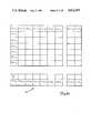
- Curvature correction datais generated by computer 200 through the use of a flexible template 250 as illustrated in FIG. 32.
- template 250has a linear pattern of indicia 252 which can include a line 254 and hatch marks 256A-256G at known and preferably evenly spaced locations thereabout.
- Template 250is shaped in such a manner as to correspond to the curvature of the finger, with line 254 oriented perpendicular to an imaginary axis 139 representing the longitudinal axis of finger 132. Line 254 will therefore be parallel to an X-base curve axis 140 of finger 132.
- Shaped template 250is then positioned within groove 102 of prism 20A with pattern of indicia 252 oriented in the above-identified manner.
- Curvature correction datais generated from template image array TIA in the following manner. All curvature distortion inherent in the transfer function of prism 20A occurs along a y-axis parallel to a vertical line through the longitudinal axis of the finger when positioned in groove 102 of prism 20A (and generally parallel to surface 106). Furthermore, it is assumed that all pixel values PVn,m for any column 1 ⁇ m ⁇ M within template image array TIA are distorted by the same amount. That is, the amount of distortion for all pixel values PV1 ⁇ n ⁇ N,M, for example, are equal.
- OFF1 and OFF2equal seven
- OFF3 and OFF4equal six
- OFF9 and OFF10equal three.
- a curvature correction table of curvature correction or offset data OFF1-OFFMis generated by computer 200 and stored in RAM 202 or ROM 204.
- Computer 200utilizes the offset data in the curvature correction table to generate curvature corrected array CCA of curvature corrected pixel values PVn,m C from unhaired array UA. Computer 200 does this by determining pixel values PVn,m C of curvature corrected array CCA as a function of the pixel values PVn,m U in the unhaired array and offsets OFFm, as described by equation 33, below.
- PV10,9 CPV7,9 U .
- curvature corrected array CCA of curvature corrected pixel values PVn,m Ccan be produced.
- pixel values PVn,m C for 1 ⁇ n ⁇ OFFm of a given row 1 ⁇ m ⁇ M of curvature corrected array CCAthere will obliously be no pixel values PVh,m U within unhaired array VA to "translate.”
- These pixel values PVn,m Care simply set equal to PVMAX or PVMIN, as they define the edge of the fingerprint image represented by array CCA.
- fingerprint images produced by finger prisms 20A-20D and slap print prisms 18 and 18'will have vertical or Y-axis size or scale errors due to the observation OA at which fingerprint 134 of finger 132 is imaged (FIG. 15).
- This vertical scale erroris compounded on fingerprint images produced by finger prisms 20A-20D since portions of fingerprint 134 near tip 145 curve upward, effectively increasing the observation angle at these locations.
- This vertical scale errorcan also be thought of a paralax error.
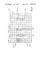
- computer 200processes curvature corrected array CCA in accordance with a Vertical Scaling program to generate a vertically scaled array VA of vertically scaled pixel values PVn,m V as illustrated in FIG. 35.
- a table of vertical scale correction datais generated for each prism 20A-20D, 18 and 18' within system 10, and stored in either RAM 202 or ROM 204.
- Computer 200utilizes the table of vertical scale correction data to generate vertically scaled array VA.
- a template 270will have a pattern of indicia 272A-272H which are spaced about a Y-axis 274 by known and preferably equal distances D30. Template 270 is positioned on finger-receiving surface 150 of prism 18 with axis 274 oriented parallel to a longitudinal axis such as 139 of a finger such as 132 when positioned on prism 18.
- An image 276 of the pattern of indicia 272A-272Hwill be propagated from image propagation surface 156, imaged by camera 28 (FIG. 2), and the data representative of this image processed by computer 200 in accordance with the various programs described above until a curvature corrected array CCA of image 276 is generated.
- a portion of a curvature corrected array CCA representative of image 276 and the pattern of indicia 272A-272His illustrated diagramatically in FIG. 37.
- Indicia 272A-272Eare illustrated graphically in FIG. 37 for purposes of example. However, it is to be understood that the magnitude of the image at the particular pixel locations of indicia 272A-272H in curvature corrected array CCA are actually represented by pixel values PVn,m C .
- indicia 272A-272Hare separated by known distances on template 270, these known distances would correspond to predetermined numbers of pixel location PLn,m in the vertical or "n" direction of curvature corrected array CCA.
- indicia 272A-272Hare separated by equal known distances D30.
- the representation of each indicia 272A-272Hwould be separated from each other in the vertical direction of array CCA by the same predetermined number (e.g., three) pixel locations PLn,m.
- predetermined numbere.g., three
- indicia 272A and 272Bare compressed, separated by no pixel locations PLn,m, and adjacent to one another.
- Indicia 272B and 272Care also compressed, but not quite as much, and are separated by one pixel location PLn,m.
- Indicia 272D and 272Eare vertically expanded from their normal positional relationship, and separated by four pixel locations PLn,m.
- a table 280 of vertical scale correction data generated by computer 200is illustrated graphically in FIG. 38.
- Data within table 280characterizes locations of pixel values PVn,m V in vertically scaled array VA as a function of the vertical location within curvature corrected array CCA at which the pixel value should be taken.
- indicia 272Bshould be spaced from 72A by three pixel locations PLn,m in the example used above.
- Pixel values PV201,m C of curvature corrected array CCAshould therefore be positioned in row 204 of vertically scaled array VA.
- Table 280includes data which characterizes pixel values PV204,m V as being equal to pixel values PV201,m C of curvature corrected array CCA.
- Computer 200thereby "fills in” this lost information by inserting or repeating pixel values PV201,m V -PV203,m V of vertically scaled array VA with information at one of either pixel values PV200,m C or PV201,m C of the curvature corrected array CCA.
- all pixel values PV201,m V -PV203,m Vare set equal to pixel value PV201,m C of curvature corrected array CCA.
- indicia 272Cshould be spaced vertically from indicia 272B by three pixel locations PLn,m. All pixel values PV203,m C of the 203rd row in curvature corrected array CCA should therefore actually be positioned in the 208th row of vertically scaled array VA. Accordingly, computer 200 generates data within table 280 associating pixel values PV203,m C of curvature corrected array CCA with pixel values PV208,m V of the vertically scaled array VA.
- Portions of the image which were lost due to compression between indicia 272B and 272Care "filled in” by repeating pixel values PV202,m C of the curvature corrected array CCA at pixel values PV205,m V -PV207,m V of vertically scaled array VA.
- Data characteristic of this filling in or repetition of pixel valuesis characterized in table 280. Procedures similar to those described above are repeated for pixel value PV212,m V of vertically scaled array VA which should actually be equal to pixel values PV206,m C in curvature corrected array CCA.
- Indicia 272D and 272Ewould also be separated by three pixel locations PLn,m were no vertical scaling errors inherent in prism 18. However, indicia 272D and 272E have been "expanded" by the optical properties of prism 18, and they are actually separated by four pixel locations PLn,m. In other words, pixel values PV211,m C in curvature corrected array CCA should actually be spaced from pixel values PV212,m V of vertical scaled array VA (which correspond to pixel values PV206,m C in curvature corrected array CCA) by three pixel locations PLn,m. Accordingly, computer 200 causes data representative of the fact that pixel values PV216,m V of vertically scaled array VA should actually be equal to pixel values PV211,m C of curvature corrected array CCA in table 280.
- indicia 272D and 272Ewere expanded, portions of the image therebetween are redundant and must be eliminated.
- one row of pixel values PVn,m Cmust be eliminated from the curvature corrected array CCA.
- computer 200has eliminated pixel values PV208,m C of curvature corrected array CCA.
- computer 200utilizes data stored in memory and representative of table 280 (vertical scale correction data) along with pixel values PVn,m C of curvature corrected array CCA. For each pixel value PVn,m V of vertically scaled array VA, computer 200 accesses table 280 to determine from which row of curvature corrected array CCA the pixel value PVn,m C should be taken. For example, to produce a vertically scaled array VA from curvature corrected array CCA shown in FIG. 31 utilizing vertical scale correction data in table 280, pixel values PV200,m V will be set equal to corresponding pixel values PV200,m C of curvature corrected array CCA.
- Pixel values PV200,200 V of vertically scaled array VAwill, for example, be set equal to pixel value PV200, 200 C of curvature corrected array CCA.
- Pixel values PV211,m V of vertically scaled array VAwill be said equal to corresponding pixel values PV205,m C .
- Pixel value PV211,200 V of vertically scaled array VAwill, for example, be set equal to pixel value PV205,200 C of curvature corrected array CCA.
- all pixel values PV1,m V and PVN,m Vare set equal to values PVMAX.
- Computer 200will then store data representative of vertically scaled array VA in RAM 202.
- fingerprint images produced by finger prisms 20A-20Dwill have horizontal or X-axis size or scale errors due to the observation angle OA at which finger 134 of finger 132 is imaged, and the fact that portions of the fingerprint are positioned about a curved surface such as that represented by X-base curve axis 140 at sides 144 of fingerprint 143. Since the image is taken at an observation angle other than 90° with respect to the "plane" of the fingerprint at any particular point, two distances along X-axis 140 are "compressed” along the horizontal axis of the fingerprint image such as that represented by vertically scaled array VA. In other portions of the image, distances about X-axis 140 can be "expanded” from their true distance on the fingerprint.
- computer 200processes vertically scaled array VA in accordance with a Horizontal Scaling program to generate a horizontally scaled array HA of horizontally scaled pixel values PVn,m H as illustrated in FIG. 39.
- a table 310 of vertical scale correction datasuch as that illustrated in FIG. 40 is generated for each prism 20A-20D within system 10, and stored in either RAM 202 or ROM 204.
- Computer 200utilizes the table such as 310 of horizontal scale correction data to generate horizontally scaled array HA.
- a template 250has a pattern of indicia 252 which includes hatch marks 256A-256G spaced about a line 254 by known and preferably equal distances. Template 250 is then shaped to conform to groove 102 of prism 20A, and positioned within the group in such a manner that line 254 is perpendicular to a longitudinal axis of the groove. This procedure is performed in a manner identical to that previously described with reference to the Curvature Correction program.
- An image of pattern of indicia 252 and hatch marks 256A-256Gwill be propagated from image propagation surface 106, imaged by camera 28 (FIG. 2), and data representative of this image processed by computer 200 in accordance with the various programs described above until a vertically scaled array VA of the image is generated.
- FIG. 41A portion of vertically scaled array VA representative of the image of hatch marks 256A-256E is illustrated diagrammatically in FIG. 41.
- Indicia 256A-256Eare illustrated graphically in FIG. 41 for purposes of example. However, it is to be understood that the magnitude of the image at the particular pixel locations of indicia 256A-256E in vertically scaled array VA are actually represented by pixel values PVn,m V .
- hatch marks 256A-256Eare separated by known distances on template 250, these known distances would correspond to predetermined numbers of pixel locations PLn,m in the horizontal or "m" direction of vertically scaled array VA.
- hatch marks 256A-256Gare separated by known distances. Were there are no horizontal scale error, the representation of each hatch mark 256A-256G would be separated from each other in the horizontal direction of array VA by the same predetermined number (e.g., three) pixel locations PLn,m. However, due to the scale errors inherent in prism 20A, hatch marks 256A-256G will be separated by differing numbers of pixel locations PLn,m. In the example shown in FIG.
- hatch marks 256A and 256Bare compressed, separated by no pixel locations PLn,m, and adjacent to one another.
- Hatch marks 256B and 256Care compressed, but not quite as much, and are separated by one pixel location PLn,m.
- Hatch marks 256D and 256Eare horizontally expanded from their normal positional relationship, and separated by four pixel locations PLn,m.
- Data within table 310characterizes locations of pixel values PVn,m H in horizontally scaled array HA as a function of the horizontal location within vertically scaled array VA at which the pixel value should be taken.
- hatch mark 256Bshould be spaced from 256A by three pixel locations PLn,m in the example used above.
- Pixel values PVn,301 V of vertically scaled array VAshould therefore be positioned in column 304 of horizontally scaled array HA.
- Table 310therefore, includes data which characterizes pixel values PVn,304 H as being equal to pixel values PVn,301 V of vertically scaled array VA.
- hatch mark 256Cshould be spaced horizontally from hatch mark 256B by three pixel locations PLn,m. All pixel values PVn,303 V of the 303rd column in the vertically scaled array VA should therefore actually be positioned in the 208th column of horizontally scaled array VA. Accordingly, computer 200 generates data within table 310 associating pixel values PVn,303 V of vertically scaled array VA with pixel values PVn,308 H of the horizontally scaled array HA.
- Portions of the image which were lost due to the compression between hatch marks 256B and 256Care "filled in” by repeating pixel values PVn,302 V of the vertically scaled array VA at pixel values PVn,305 H -PVn,307 H of horizontally scaled array HA.
- Data characteristic of this filling in or repetition of pixel valuesis characterized in table 310. Procedures similar to those described above are repeated for pixel values PVn,312 H of horizontally scaled array HA which should actually be equal to pixel values PVn,306, V of the vertically scaled array VA.
- Hatch marks 256D and 256Ewould also be separated by three pixel locations PLn,m were no vertical scaling errors inherent in prism 20A. However, hatch marks 256D and 256E have been "expanded" by the optical properties of prism 20A, and they are actually separated by four pixel locations PLn,m.
- pixel values PVn,311, V in vertically scaled array VAshould actually be spaced from pixel values PVn,312 H of horizontally scaled array HA (which correspond to pixel values PVn,306 V in vertically scaled array VA) by three pixel locations PLn,m.
- computer 200causes data representative of the fact that pixel values PVn,316, H of horizontally scaled array HA should actually be equal to pixel values PVn,311 V of vertically scaled array VA in table 310.
- computer 200utilizes data stored in memory and representative of table 310 (horizontal scale correction data) along with pixel values PVn,m V of vertically scaled array VA. For each pixel value PVn,m H of horizontally scaled array HA, computer 200 accesses table 310 to determine from which column of vertically scaled array VA the pixel value PVn,m H should be taken. For example, to produce horizontally scaled array HA from vertically scaled array VA shown in FIG. 35 utilizing horizontal scale correction data in table 310, pixel values PVn,300 H will be set equal to corresponding pixel values PVn,300 V of vertically scaled array VA.
- Pixel values PV300,300 H of horizontally scaled array HAwill, for example, be set equal to pixel value PV300,300 V of vertically scaled array VA.
- pixel values PVn,311 H of horizontally scaled array HAwill be set equal to corresponding pixel values PVn,305 V .
- all pixel values PVn,1 H and PVn,M Hare set equal to values PVMAX.
- Computer 200will then store data representative of horizontally scaled array HA and RAM 202.
- a horizontally scaled array HA of horizontally scaled pixel values PVn,m H representative of the fingerprint imageis stored in RAM 202.
- Each pixel value PVn,m His an eight-bit digital value representing intensity of the image at that particular discrete or pixel location PLn,m. This data will be utilized by printer 16 to print an enhanced visual representation of the fingerprint image.
- printer 16is a matrix printer capable of printing in a gray scale at discrete locations.
- computer 200retrieves pixel values PVn,m H of horizontally scaled array HA from RAM 202, maps these pixel values into a proper format, and transmits this data to the printer.
- Printer 16will then print a visual representation of the fingerprint image with the intensity at each discrete printed location determined by the pixel value PVn,m H .
- printer 16is a dot matrix printer, and incapable of utilizing pixel values PVn,m H to print a gray scale image at discrete locations or dots. At each discrete location on applicant card 15, printer 16 can either leave the spot blank, or make it black. As a result, computer 200 implements a Threshold program to determine whether each pixel value PVn,m H of the horizontally scaled array HA should be represented as a white or black spot by printer 16 on card 15.
- Threshold programcomputer 200 compares each pixel value PVn,m H to a print threshold value TP. If the pixel value PVn,m H is less than the threshold value TP, this pixel value is to represent a "black” or printed region on applicant card 15, and computer 200 accordingly sets the pixel value to zero or "0". If the pixel value PVn,m H is greater than or equal to threshold value TP, this particular pixel value is to represent a white portion of the image, and computer 200 accordingly sets a pixel value equal to one or "1".
- Threshold value TPcan vary depending upon a desired appearance of the fingerprint image. In one embodiment, threshold value TP is a digital value representative of an intensity halfway between the two hundred and fifty-six (i.e.
- threshold value TPshould be set to a value lower than 128. If it is desired to have the white portions of the image (ridges 136) to have a finer width, threshold value TP should be set to a level higher than 128.
- computer 200Having generated a Thresholded array of enhanced pixel values PVn,m H , computer 200 stores these pixel values in RAM 202. In response to print signals, computer 200 will transmit these bits sequentially in a standard printer format to printer 16. In response, printer 16 will print the enhanced fingerprint image onto applicant card 15.
- FIGS. 1 and 42-47Operation of fingerprinting system 10 is described with reference to FIGS. 1 and 42-47.
- computer 200Upon initial power-up, computer 200 will run a series of diagnostics which verify correct operation of computer 200, RAM 202, and ROM 204. After passing these diagnostics, data terminal 6 will generate a copyright notice which will be displayed on monitor 7 for several seconds. Following the copyright notice, data terminal 6 will generate and display on its monitor 8 a Main Display menu 300 illustrated in FIG. 42.
- Option 1by sequentially pressing the "1" and RETURN keys of keyboard 7 of data terminal 6 whenever a new booking is being processed.
- System 10is then cleared of information from a previous booking, and reset so as to be ready to accept new information.
- Option 2is selected if it is desired to capture only one fingerprint. This is done if it is desired to test system capabilities, or to edit a poor previously captured print. Option 2 is selected when the operator sequentially presses the "2" and RETURN keys of keyboard 7.
- Option 3is selected by sequentially pressing the "3" and RETURN keys of keyboard 7. In response to this option, the operator will be asked a series of questions by means of prompts displayed on monitor 8 of data terminal 6. These questions are answered by pressing the "Y" key of keyboard 7 to answer “yes", or by pressing the "N" key to answer “no.”
- Options which can be selected in this mannerinclude a High Contrast Capture Option which allows a very quick capture of print, but with relatively low quality due to the high contrast. The operator can also get an enlarged printed copy of one of the prints if desired. If the Enlarged Print Option is selected, both a life-size and four times normal size image of a fingerprint can be printed by printer 16.
- the operatoris asked if they would like to approve the print twice.
- the first chance to approve the printcomes after capture, and the second chance comes after the image has been visually enhanced by the image enhancement software programs.
- printsare approved only once, that being after processing has been completed.
- system 10enters a capture mode during which all ten individual fingerprints, plus slap prints from both the left and right hands, will be captured. This procedure is implemented with the assistance of key pad 19 and display 13 on optics/processor unit 12.
- computer 200will first actuate motor 76 to drive slap/finger image selection optics 26 to the finger prism select position illustrated in FIG. 2 (if optics 26 is not already so positioned). Signals representative of this positioning are provided to computer 200 by microswitch 89, where upon actuation of motor 76 is terminated. Computer 200 wil then cause LED 316A of left hand indicia 312 to be lit, indicating a prompt that a fingerprint of the left thumb is to be captured. Simultaneously, computer 200 cause LEDs 21C and 21D to be lit, thereby illuminating keys 17C and 17D.
- the operatorwill then move trolley 42, using lever 52, to position a finger prism 20A-20D having the properly sized groove 102 for the thumb of the particular person being fingerprinted within aperture 51.
- the person being fingerprintedwill then position their thumb within groove 102 of the selected prism 20A-20D, and adjust their finger within the groove while the operator observes image quality on monitor 14.
- the operatorwill actuate CAPTURE key 17C on key pad 19.
- This imageis then "frozen", with digitizer 206 digitizing the data provided by TV camera 24.
- This datais then processed in accordance with the software programs described above to produce an array of data characterizing the enhanced fingerprint image.
- This datais then stored within RAM 202. If the person being fingerprinted was an amputee and did not have a left thumb, the operator would have actuated AMP key 17D.
- Computer 200then stores data characteristic of this action.
- computer 200After the capture and processing of the left thumb fingerprint, computer 200 will cause LED 316B to be illuminated thereby prompting the operator that the left index finger is to be fingerprinted. The above described procedures are then repeated, with prompts for each of the ten fingers of the two hands of the person being fingerprinted being made.
- a promptwill be displayed on monitor 8 of data terminal 6 indicating that slap or plain prints for the left hand are to be taken.
- Computer 200will also actuate motor 76 so as to drive mounting plate 60 to its slap print image selection position.
- Computer 200will receive a signal from microswitch 87, and deactivate motor 76, when selection optics 26 are properly positioned at the slap image position illustrated in FIG. 3B.
- CAPTURE key 17C and AMP key 17Dwill also be lit. The person to be fingerprinted will then position the index, middle, ring and little fingers of the left hand on finger receiving surface 150 of slap print prism 18'.
- Main Display menu 300which is shown in FIG. 42 will again be displayed on monitor 8 of data terminal 6.
- the operatorcan then select Option 3 to enter demographic information regarding the person whose fingerprints have just been taken as well as to enter department information used by the police or other organization performing the fingerprinting.
- data terminal 6will display on its monitor 8 a Demographic/Department Information menu such as 320 (FIG. 45) which requests the operator to enter all necessary demographic and department information.
- the operatorcan then enter this demographic information using the various keys of keyboard 7 of data terminal 6 in a standard manner.
- Main Display menu 300can then again be displayed when the operator presses the RETURN key once all demographic and department information has been entered into terminal 6.
- Option 4After all fingerprints have been captured and demographic/department information entered, the operator can select Option 4 to have all of this information printed on a standardized booking or applicant card such as 15 illustrated in FIG. 47.
- Applicant card 15has standardized locations for all the various fingerprints which have been capured, as well as the demographic information and department information which has been entered into terminal 6. Card 15 will be inserted into printer 16 in an indexed manner.
- computer 200causes all of the information retrieved from RAM 202 and to be printed at the proper locations on card 15.
- the optical fingerprinting system of the present inventionoffers a number of significant advantages over those of the prior art. Both individual fingerprint and slap print images can be optically obtained. A real-time display of the fingerprint being imaged can be observed and analyzed prior to its capture. Grooves within the finger prisms are contoured in such a manner as to provide an optimum amount of contact between the fingerprint and the prism.
- the lens trolleywhich has finger prisms with a variety of different sized grooves, permits use of the system with a wide range of finger sizes.
- the lensed surface of the finger and slap prismsreduces vertical and horizontal scale errors, as well as curvature correction errors. Furthermore, remaining scale and curvature errors are eliminated, and other characteristics of the fingerprint image greatly enhanced, through the use of the Image Enhancement programs.
- the systemis also designed to be very user friendly.
Landscapes
- Engineering & Computer Science (AREA)
- Physics & Mathematics (AREA)
- Health & Medical Sciences (AREA)
- General Physics & Mathematics (AREA)
- Theoretical Computer Science (AREA)
- Life Sciences & Earth Sciences (AREA)
- Biomedical Technology (AREA)
- Molecular Biology (AREA)
- Biophysics (AREA)
- Pathology (AREA)
- Human Computer Interaction (AREA)
- Heart & Thoracic Surgery (AREA)
- Medical Informatics (AREA)
- Multimedia (AREA)
- Surgery (AREA)
- Animal Behavior & Ethology (AREA)
- General Health & Medical Sciences (AREA)
- Public Health (AREA)
- Veterinary Medicine (AREA)
- Collating Specific Patterns (AREA)
- Image Input (AREA)
Abstract
Description
PDVn,m=PVn,m.sub.N -SAVn,m. EQ. 5
IEPVn,m=PDVn,m+K. Eq. 6
PVn,m.sub.E =PVMIN if IEPVn,m<PVMIN. Eq. 7
PVn,m.sub.E =IEPVn,m if PVMIN≦IEPVn,m≦PVMAX. Eq. 8
PVn,m.sub.E =PVMAX if IEPVn,m>PVMAX. Eq. 9
HorizDifn,m=|PV n,m.sub.E -PVn,m+l.sub.E |Eq. 11
VertDifn,m=|PVn,m.sub.E -PVn+l,m.sub.E | Eq. 12
PosDifn,m=|PVn,m.sub.E -PVn-l,m+l.sub.E |Eq. 13
NegDifn,m=|PVn,m.sub.E -PVn+l, m+l.sub.E |Eq. 14
______________________________________HDSum.sub.230xx = ΣHorizDifn,m Eq. 15 (For all PVn,m.sub.E ofVDSum.sub.230xx = ΣVertDifn,m Eq. 16 subarray 230xx forPDSum.sub.230xx = ΣPosDifn,m Eq. 17 which difference valuesNDSum.sub.230xx = ΣNegDifn,m Eq. 18 were computed)HDSum.sub.232xx = ΣHorizDifn,m Eq. 19 (For all PVn,m.sub.E ofVDSum.sub.232xx = ΣVertDifn,m Eq. 20 subarray 232xx forPDSum.sub.232xx = ΣPosDifn,m Eq. 21 which difference valuesNDSum.sub.232xx = ΣNegDifn,m Eq. 22 were computed)______________________________________
__________________________________________________________________________RSPVn,m.sub.E = (2 PVn,m.sub.E + PVn,m - 1.sub.E + PVn,m + 1.sub.E)/4 Eq. 23 (when the dominant direction of the regular subarray is horizontal)RSPVn,m.sub.E = (2 PVn,m.sub.E + PVn - 1,m.sub.E + PVn + 1,m.sub.E)/4 Eq. 24 (when the dominant direction of the regular subarray is vertical).RSPVn,m.sub.E = (2PVn,m.sub.E + PVn - 1, m + 1.sub.E + PVn + 1, m Eq. 25b.E)/4 (when the dominant direction of the regular subarray is positive slope).RSPVn,m.sub.E = (2PVn,m.sub.E + PVn - 1,m - 1.sub.E + PVn + 1,m Eq. 26b.E)/4 (when the dominant direction of the regular subarray is negative slope).Offset subarray directional filtered pixel valuesOSPVn,m.sub.E can be computed in a similar manner using equations 27-30.OSPVn,m.sub.E = (2PVn,m.sub.E + PVn,m - 1.sub.E + PVn,m + 1.sub.E)/4 Eq. 27 (if the dominant direction of the offset subarray is horizontal).OSPVn,m.sub.E = (2PVn,m.sub.E + PVn - 1,m.sub.E + PVn + 1,m.sub.E)/4 Eq. 28 (if the dominant direction of the offset subarray is vertical).OSPVn,m.sub.E = (2PVn,m.sub.E + PVn - 1,m + 1.sub.E + PVn + 1,m Eq. 29b.E)/4 (if the dominant direction of the offset subarray is positive slope).OSPVn,m.sub.E = (2PVn,m.sub.E + PVn - 1,m - 1.sub.E + PVn + 1,m Eq. 30b.E)/4 (if the dominant direction of the offset subarray is negative slope).__________________________________________________________________________
PVn,m.sub.D =(RSPVn,m.sub.E +OSPVn,m.sub.E)/2 Eq. 31
PVn,m.sub.U =PVn,m.sub.D Eq. 32a
PVn,m-1.sub.D, PVn,m.sub.D, . . . and PVn,m+W.sub.D =PVMAX Eq. 32b
PVn,m.sub.U =PVn,mp.sub.D for 1<n<N, M-W<m≦M. Eq. 32c
PVn,m.sub.C =PVn-OFFm,m.sub.U Eq. 33.
Claims (7)
Priority Applications (1)
| Application Number | Priority Date | Filing Date | Title |
|---|---|---|---|
| US07/020,331US4811414A (en) | 1987-02-27 | 1987-02-27 | Methods for digitally noise averaging and illumination equalizing fingerprint images |
Applications Claiming Priority (1)
| Application Number | Priority Date | Filing Date | Title |
|---|---|---|---|
| US07/020,331US4811414A (en) | 1987-02-27 | 1987-02-27 | Methods for digitally noise averaging and illumination equalizing fingerprint images |
Publications (1)
| Publication Number | Publication Date |
|---|---|
| US4811414Atrue US4811414A (en) | 1989-03-07 |
Family
ID=21798037
Family Applications (1)
| Application Number | Title | Priority Date | Filing Date |
|---|---|---|---|
| US07/020,331Expired - Fee RelatedUS4811414A (en) | 1987-02-27 | 1987-02-27 | Methods for digitally noise averaging and illumination equalizing fingerprint images |
Country Status (1)
| Country | Link |
|---|---|
| US (1) | US4811414A (en) |
Cited By (134)
| Publication number | Priority date | Publication date | Assignee | Title |
|---|---|---|---|---|
| US5003618A (en)* | 1989-07-14 | 1991-03-26 | University Of Pittsburgh Of The Commonwealth System Of Higher Education | Automatic adaptive anisotropic digital filtering and biasing of digitized images |
| WO1991006920A1 (en)* | 1989-11-02 | 1991-05-16 | Tms, Incorporated | Non-minutiae automatic fingerprint identification system and methods |
| WO1992004689A1 (en)* | 1990-08-31 | 1992-03-19 | Digital Biometrics, Inc. | Method and apparatus for capturing skin print images |
| USD325196S (en) | 1991-03-08 | 1992-04-07 | Digital Biometrics, Inc. | Cabinet for optical imaging of fingerprints |
| US5105467A (en)* | 1989-11-28 | 1992-04-14 | Kim Bong I | Method of fingerprint verification |
| US5113137A (en)* | 1989-09-12 | 1992-05-12 | Hitachi, Ltd. | Method and apparatus for reducing image noises |
| USD346158S (en) | 1991-03-25 | 1994-04-19 | Digital Biometrics, Inc. | Cabinet housing for optical imaging of fingerprints |
| WO1994022370A1 (en)* | 1993-04-01 | 1994-10-13 | British Technology Group Limited | Biometric identification of individuals |
| WO1994022371A3 (en)* | 1993-03-31 | 1994-12-08 | Digital Biometrics Inc | Portable fingerprint scanning apparatus for identification verification |
| EP0644737A4 (en)* | 1992-06-08 | 1995-08-23 | Univ Washington | PROCESS FOR IMAGING SOLID TUMORS, CORTICAL FUNCTION AND NERVES. |
| US5699798A (en)* | 1990-08-10 | 1997-12-23 | University Of Washington | Method for optically imaging solid tumor tissue |
| USD389817S (en) | 1996-06-04 | 1998-01-27 | Fujitsu Denso, Ltd. | Fingerprint distinction reader |
| WO1998010370A1 (en)* | 1996-09-09 | 1998-03-12 | ARETé ASSOCIATES | Systems and methods with identity verification by comparison and interpretation of skin patterns such as fingerprints |
| US5732148A (en)* | 1994-09-16 | 1998-03-24 | Keagy; John Martin | Apparatus and method for electronically acquiring fingerprint images with low cost removable platen and separate imaging device |
| US5796857A (en)* | 1993-10-21 | 1998-08-18 | Nec Corporation | Apparatus for fingerprint verification using different verification method in accordance with quality grade data |
| US5796858A (en)* | 1996-05-10 | 1998-08-18 | Digital Persona, Inc. | Fingerprint sensing system using a sheet prism |
| WO1998052157A1 (en) | 1997-05-16 | 1998-11-19 | Authentec, Inc. | Fingerprint sensor with gain control features and associated methods |
| US5845639A (en)* | 1990-08-10 | 1998-12-08 | Board Of Regents Of The University Of Washington | Optical imaging methods |
| WO1998046114A3 (en)* | 1997-04-11 | 1999-04-08 | Arete Associates | Systems & methods with identity verification by streamlined comparison & interpretation of fingerprints and the like |
| FR2769823A1 (en)* | 1997-10-17 | 1999-04-23 | Thomson Csf | DEVICE AND METHOD FOR INPUT OF FINGERPRINTS |
| US5903225A (en)* | 1997-05-16 | 1999-05-11 | Harris Corporation | Access control system including fingerprint sensor enrollment and associated methods |
| US5920640A (en)* | 1997-05-16 | 1999-07-06 | Harris Corporation | Fingerprint sensor and token reader and associated methods |
| US5940526A (en)* | 1997-05-16 | 1999-08-17 | Harris Corporation | Electric field fingerprint sensor having enhanced features and related methods |
| US5953441A (en)* | 1997-05-16 | 1999-09-14 | Harris Corporation | Fingerprint sensor having spoof reduction features and related methods |
| US5963657A (en)* | 1996-09-09 | 1999-10-05 | Arete Associates | Economical skin-pattern-acquisition and analysis apparatus for access control; systems controlled thereby |
| US5987156A (en)* | 1996-11-25 | 1999-11-16 | Lucent Technologies | Apparatus for correcting fixed column noise in images acquired by a fingerprint sensor |
| US6002787A (en)* | 1992-10-27 | 1999-12-14 | Jasper Consulting, Inc. | Fingerprint analyzing and encoding system |
| US6035398A (en)* | 1997-11-14 | 2000-03-07 | Digitalpersona, Inc. | Cryptographic key generation using biometric data |
| US6038332A (en)* | 1997-09-05 | 2000-03-14 | Digital Biometrics, Inc. | Method and apparatus for capturing the image of a palm |
| US6067368A (en)* | 1996-01-26 | 2000-05-23 | Authentec, Inc. | Fingerprint sensor having filtering and power conserving features and related methods |
| US6088585A (en)* | 1997-05-16 | 2000-07-11 | Authentec, Inc. | Portable telecommunication device including a fingerprint sensor and related methods |
| US6088471A (en)* | 1997-05-16 | 2000-07-11 | Authentec, Inc. | Fingerprint sensor including an anisotropic dielectric coating and associated methods |
| US6097035A (en)* | 1999-02-22 | 2000-08-01 | Digital Persona, Inc. | Fingerprint detection apparatus with partial fingerprint images |
| US6098330A (en)* | 1997-05-16 | 2000-08-08 | Authentec, Inc. | Machine including vibration and shock resistant fingerprint sensor and related methods |
| US6111977A (en)* | 1997-04-17 | 2000-08-29 | Cross Match Technologies, Inc. | Hand-held fingerprint recognition and transmission device |
| US6122737A (en)* | 1997-11-14 | 2000-09-19 | Digital Persona, Inc. | Method for using fingerprints to distribute information over a network |
| US6125192A (en)* | 1997-04-21 | 2000-09-26 | Digital Persona, Inc. | Fingerprint recognition system |
| US6178255B1 (en) | 1998-04-28 | 2001-01-23 | Cross Match Technologies, Inc. | Individualized fingerprint scanner |
| US6188781B1 (en) | 1998-07-28 | 2001-02-13 | Digital Persona, Inc. | Method and apparatus for illuminating a fingerprint through side illumination of a platen |
| WO2001011550A1 (en)* | 1999-08-09 | 2001-02-15 | Cross Match Technologties, Inc. | Method, system, and computer program product for a gui to fingerprint scanner interface |
| US6196226B1 (en) | 1990-08-10 | 2001-03-06 | University Of Washington | Methods and apparatus for optically imaging neuronal tissue and activity |
| US6201886B1 (en)* | 1996-09-25 | 2001-03-13 | Sony Corporation | Image collation device |
| US6263090B1 (en) | 1997-05-19 | 2001-07-17 | Cross Match Technologies, Inc. | Code reader fingerprint scanner |
| US6272562B1 (en) | 1999-05-28 | 2001-08-07 | Cross Match Technologies, Inc. | Access control unit interface |
| US6282303B1 (en) | 1998-06-02 | 2001-08-28 | Digital Persona, Inc. | Method and apparatus for scanning a fingerprint using a linear sensor within a cursor control device |
| US20020054695A1 (en)* | 1998-09-16 | 2002-05-09 | Vance C. Bjorn | Configurable multi-function touchpad device |
| US20020090147A1 (en)* | 2000-12-18 | 2002-07-11 | Scott Walter G. | Palm scanner using a programmable nutating mirror for increased resolution |
| US20020131624A1 (en)* | 2000-08-11 | 2002-09-19 | Yury Shapiro | Fingerprint imaging device with fake finger detection |
| US20020196476A1 (en)* | 2001-06-22 | 2002-12-26 | Tatsuya Ozaki | Device for reading an image, apparatus for forming an image, communication device, and method for detecting an abnormal portion such as a black line in an image |
| US20030016427A1 (en)* | 2001-04-26 | 2003-01-23 | Arnold Joe F. | Silicon rubber surfaces for biometric print TIR prisms |
| US20030091219A1 (en)* | 1999-08-19 | 2003-05-15 | Martinez Chris J. | Method and apparatus for rolled fingerprint capture |
| US20030113000A1 (en)* | 2001-12-19 | 2003-06-19 | Fuji Xerox Co., Ltd. | Image collating apparatus for comparing/collating images before/after predetermined processing, image forming apparatus, image collating method, and image collating program product |
| US20030123716A1 (en)* | 1999-08-09 | 2003-07-03 | Cross Match Technologies, Inc. | System and method for sending a packet with position address and line scan data over an interface cable |
| US20030133143A1 (en)* | 2002-01-17 | 2003-07-17 | Cross Match Technology, Inc. | Biometric imaging system and method |
| US20030133103A1 (en)* | 2002-01-17 | 2003-07-17 | Arnold Joseph F. | Systems and methods for illuminating a platen in a print scanner |
| US20030149343A1 (en)* | 2001-09-26 | 2003-08-07 | Cross Match Technologies, Inc. | Biometric based facility security |
| US20030197593A1 (en)* | 2002-04-19 | 2003-10-23 | Cross Match Technologies, Inc. | Systems and methods utilizing biometric data |
| US20030200446A1 (en)* | 2002-04-19 | 2003-10-23 | Cross Match Technologies, Inc. | System and methods for access control utilizing two factors to control access |
| US20030206287A1 (en)* | 2002-01-17 | 2003-11-06 | Cross Match Technologies, Inc. | Light wedge for illuminating a platen in a print scanner |
| US6671540B1 (en) | 1990-08-10 | 2003-12-30 | Daryl W. Hochman | Methods and systems for detecting abnormal tissue using spectroscopic techniques |
| US20040016811A1 (en)* | 2002-04-19 | 2004-01-29 | Cross Match Technologies, Inc. | Mobile handheld code reader and print scanner system and method |
| US6687391B1 (en) | 1999-10-22 | 2004-02-03 | Cross Match Technologies, Inc. | Adjustable, rotatable finger guide in a tenprint scanner with movable prism platen |
| US6744910B1 (en) | 1999-06-25 | 2004-06-01 | Cross Match Technologies, Inc. | Hand-held fingerprint scanner with on-board image normalization data storage |
| US20040109590A1 (en)* | 2002-08-02 | 2004-06-10 | Cannon Gregory L. | System and method for counting ridges in a captured print image |
| US20040156555A1 (en)* | 1999-08-09 | 2004-08-12 | Cross Match Technologies, Inc. | Calibration and correction in a fingerprint scanner |
| US20040170303A1 (en)* | 2003-02-28 | 2004-09-02 | Cross Match Technology, Inc. | Dynamic image adaption method for adjusting the quality of digital prints |
| US20040228506A1 (en)* | 2003-05-12 | 2004-11-18 | Haddad Waleed S. | Lid and housing apparatus and method or non-contact fingerprint imager |
| US20050047631A1 (en)* | 2003-08-26 | 2005-03-03 | Cross Match Technologies, Inc. | Method and apparatus for rolled fingerprint image capture with variable blending |
| US20050044909A1 (en)* | 2003-08-28 | 2005-03-03 | Volker Lange | Knob cylinder with biometrical sensor |
| US6886104B1 (en) | 1999-06-25 | 2005-04-26 | Cross Match Technologies | Rechargeable mobile hand-held fingerprint scanner with a data and power communication interface |
| US6952489B1 (en)* | 2000-09-29 | 2005-10-04 | Hewlett-Packard Development Company, L.P. | Fingerprint verification method having band detection |
| US6956608B1 (en) | 2000-08-11 | 2005-10-18 | Identix Incorporated | Fingerprint imaging device including an optical plate having microreflectors |
| US20050231576A1 (en)* | 2001-06-22 | 2005-10-20 | Lee David L | Color reproduction process |
| US6961453B2 (en) | 2001-08-31 | 2005-11-01 | Secugen Corporation | Method for extracting fingerprint feature data using ridge orientation model |
| US6983062B2 (en) | 2000-08-18 | 2006-01-03 | Cross Match Technologies, Inc. | Fingerprint scanner auto-capture system and method |
| US7020308B1 (en)* | 1999-09-14 | 2006-03-28 | Fujitsu Limited | Personal authentication system using biometrics information |
| US20060115132A1 (en)* | 2004-12-01 | 2006-06-01 | Schneider John K | Fingerprint scanning station |
| US7162060B1 (en) | 1999-08-09 | 2007-01-09 | Cross Match Technologies | Method, system, and computer program product for control of platen movement during a live scan |
| US20070047784A1 (en)* | 2005-08-30 | 2007-03-01 | Nec Corporation | Ridge direction extraction device, ridge direction extraction method, ridge direction extraction program |
| US20070060334A1 (en)* | 2000-12-08 | 2007-03-15 | Igt | Casino gambling system with biometric access control |
| US7277562B2 (en) | 2003-08-01 | 2007-10-02 | Cross Match Technologies, Inc. | Biometric imaging capture system and method |
| US20080069412A1 (en)* | 2006-09-15 | 2008-03-20 | Champagne Katrina S | Contoured biometric sensor |
| WO2011110821A1 (en) | 2010-03-12 | 2011-09-15 | Milan Momcilo Popovich | Biometric sensor |
| US8036431B1 (en)* | 1999-10-29 | 2011-10-11 | Identix Incorporated | Portable apparatus for identification verification |
| WO2013102759A2 (en) | 2012-01-06 | 2013-07-11 | Milan Momcilo Popovich | Contact image sensor using switchable bragg gratings |
| US20130200907A1 (en)* | 2012-02-06 | 2013-08-08 | Ultra-Scan Corporation | System And Method Of Using An Electric Field Device |
| US20140286546A1 (en)* | 2013-03-22 | 2014-09-25 | Suprema Inc. | Apparatus and method for processing fingerprint image |
| WO2015015138A1 (en) | 2013-07-31 | 2015-02-05 | Milan Momcilo Popovich | Method and apparatus for contact image sensing |
| WO2016156776A1 (en) | 2015-03-31 | 2016-10-06 | Milan Momcilo Popovich | Method and apparatus for contact image sensing |
| US10145533B2 (en) | 2005-11-11 | 2018-12-04 | Digilens, Inc. | Compact holographic illumination device |
| US10156681B2 (en) | 2015-02-12 | 2018-12-18 | Digilens Inc. | Waveguide grating device |
| US20190005299A1 (en)* | 2011-03-25 | 2019-01-03 | Nec Corporation | Authentication using prism |
| US10185154B2 (en) | 2011-04-07 | 2019-01-22 | Digilens, Inc. | Laser despeckler based on angular diversity |
| US10209517B2 (en) | 2013-05-20 | 2019-02-19 | Digilens, Inc. | Holographic waveguide eye tracker |
| US10234696B2 (en) | 2007-07-26 | 2019-03-19 | Digilens, Inc. | Optical apparatus for recording a holographic device and method of recording |
| US10241330B2 (en) | 2014-09-19 | 2019-03-26 | Digilens, Inc. | Method and apparatus for generating input images for holographic waveguide displays |
| US10330777B2 (en) | 2015-01-20 | 2019-06-25 | Digilens Inc. | Holographic waveguide lidar |
| US10359736B2 (en) | 2014-08-08 | 2019-07-23 | Digilens Inc. | Method for holographic mastering and replication |
| US10423222B2 (en) | 2014-09-26 | 2019-09-24 | Digilens Inc. | Holographic waveguide optical tracker |
| US10437064B2 (en) | 2015-01-12 | 2019-10-08 | Digilens Inc. | Environmentally isolated waveguide display |
| US10437051B2 (en) | 2012-05-11 | 2019-10-08 | Digilens Inc. | Apparatus for eye tracking |
| US10459145B2 (en) | 2015-03-16 | 2019-10-29 | Digilens Inc. | Waveguide device incorporating a light pipe |
| US10545346B2 (en) | 2017-01-05 | 2020-01-28 | Digilens Inc. | Wearable heads up displays |
| US10642058B2 (en) | 2011-08-24 | 2020-05-05 | Digilens Inc. | Wearable data display |
| US10670876B2 (en) | 2011-08-24 | 2020-06-02 | Digilens Inc. | Waveguide laser illuminator incorporating a despeckler |
| US10678053B2 (en) | 2009-04-27 | 2020-06-09 | Digilens Inc. | Diffractive projection apparatus |
| US10690851B2 (en) | 2018-03-16 | 2020-06-23 | Digilens Inc. | Holographic waveguides incorporating birefringence control and methods for their fabrication |
| US10690916B2 (en) | 2015-10-05 | 2020-06-23 | Digilens Inc. | Apparatus for providing waveguide displays with two-dimensional pupil expansion |
| US10732569B2 (en) | 2018-01-08 | 2020-08-04 | Digilens Inc. | Systems and methods for high-throughput recording of holographic gratings in waveguide cells |
| US10859768B2 (en) | 2016-03-24 | 2020-12-08 | Digilens Inc. | Method and apparatus for providing a polarization selective holographic waveguide device |
| US10890707B2 (en) | 2016-04-11 | 2021-01-12 | Digilens Inc. | Holographic waveguide apparatus for structured light projection |
| US10914950B2 (en) | 2018-01-08 | 2021-02-09 | Digilens Inc. | Waveguide architectures and related methods of manufacturing |
| US10942430B2 (en) | 2017-10-16 | 2021-03-09 | Digilens Inc. | Systems and methods for multiplying the image resolution of a pixelated display |
| US10983340B2 (en) | 2016-02-04 | 2021-04-20 | Digilens Inc. | Holographic waveguide optical tracker |
| US11307432B2 (en) | 2014-08-08 | 2022-04-19 | Digilens Inc. | Waveguide laser illuminator incorporating a Despeckler |
| US11378732B2 (en) | 2019-03-12 | 2022-07-05 | DigLens Inc. | Holographic waveguide backlight and related methods of manufacturing |
| US11402801B2 (en) | 2018-07-25 | 2022-08-02 | Digilens Inc. | Systems and methods for fabricating a multilayer optical structure |
| US11442222B2 (en) | 2019-08-29 | 2022-09-13 | Digilens Inc. | Evacuated gratings and methods of manufacturing |
| US11448937B2 (en) | 2012-11-16 | 2022-09-20 | Digilens Inc. | Transparent waveguide display for tiling a display having plural optical powers using overlapping and offset FOV tiles |
| US11460621B2 (en) | 2012-04-25 | 2022-10-04 | Rockwell Collins, Inc. | Holographic wide angle display |
| US11480788B2 (en) | 2015-01-12 | 2022-10-25 | Digilens Inc. | Light field displays incorporating holographic waveguides |
| US11513350B2 (en) | 2016-12-02 | 2022-11-29 | Digilens Inc. | Waveguide device with uniform output illumination |
| US11543594B2 (en) | 2019-02-15 | 2023-01-03 | Digilens Inc. | Methods and apparatuses for providing a holographic waveguide display using integrated gratings |
| US11681143B2 (en) | 2019-07-29 | 2023-06-20 | Digilens Inc. | Methods and apparatus for multiplying the image resolution and field-of-view of a pixelated display |
| US11726332B2 (en) | 2009-04-27 | 2023-08-15 | Digilens Inc. | Diffractive projection apparatus |
| US11747568B2 (en) | 2019-06-07 | 2023-09-05 | Digilens Inc. | Waveguides incorporating transmissive and reflective gratings and related methods of manufacturing |
| US12092914B2 (en) | 2018-01-08 | 2024-09-17 | Digilens Inc. | Systems and methods for manufacturing waveguide cells |
| US12140764B2 (en) | 2019-02-15 | 2024-11-12 | Digilens Inc. | Wide angle waveguide display |
| US12158612B2 (en) | 2021-03-05 | 2024-12-03 | Digilens Inc. | Evacuated periodic structures and methods of manufacturing |
| US12210153B2 (en) | 2019-01-14 | 2025-01-28 | Digilens Inc. | Holographic waveguide display with light control layer |
| US12222499B2 (en) | 2020-12-21 | 2025-02-11 | Digilens Inc. | Eye glow suppression in waveguide based displays |
| US12306585B2 (en) | 2018-01-08 | 2025-05-20 | Digilens Inc. | Methods for fabricating optical waveguides |
| US12397477B2 (en) | 2019-02-05 | 2025-08-26 | Digilens Inc. | Methods for compensating for optical surface nonuniformity |
| US12399326B2 (en) | 2021-01-07 | 2025-08-26 | Digilens Inc. | Grating structures for color waveguides |
Citations (38)
| Publication number | Priority date | Publication date | Assignee | Title |
|---|---|---|---|---|
| US3200701A (en)* | 1962-01-29 | 1965-08-17 | Ling Temco Vought Inc | Method for optical comparison of skin friction-ridge patterns |
| US3478658A (en)* | 1966-12-06 | 1969-11-18 | Farrington Business Mach | Optical fingerprint recording device |
| US3482498A (en)* | 1967-05-09 | 1969-12-09 | Trw Inc | Ridge pattern recording apparatus |
| US3581282A (en)* | 1968-12-03 | 1971-05-25 | Norman G Altman | Palm print identification system |
| US3614737A (en)* | 1969-09-08 | 1971-10-19 | Dactylog Inc | Method and apparatus for individual recognition |
| US3639905A (en)* | 1970-11-27 | 1972-02-01 | Omron Tateisi Electronics Co | Credit card system having means for sensing if object is living |
| US3648240A (en)* | 1970-01-15 | 1972-03-07 | Identification Corp | Personnel identification apparatus |
| US3743772A (en)* | 1969-11-12 | 1973-07-03 | Meldreth Electronics Ltd | Image analysing |
| US3944978A (en)* | 1974-09-09 | 1976-03-16 | Recognition Systems, Inc. | Electro-optical method and apparatus for making identifications |
| US3968476A (en)* | 1974-07-17 | 1976-07-06 | Sperry Rand Corporation | Spurious signal removal in optical processor fingerprint identification apparatus |
| US3975711A (en)* | 1974-08-30 | 1976-08-17 | Sperry Rand Corporation | Real time fingerprint recording terminal |
| US4047152A (en)* | 1975-11-03 | 1977-09-06 | Elettronica San Giorgio - Elsag - S.P.A. | Electronic character-reading system |
| US4074231A (en)* | 1975-12-17 | 1978-02-14 | Hitachi, Ltd. | Pattern processing system |
| US4107775A (en)* | 1976-03-16 | 1978-08-15 | Novar Electronics Corporation | Human body comparison using driving point parameters |
| US4120585A (en)* | 1976-11-19 | 1978-10-17 | Calspan Corporation | Fingerprint identification system using a pliable optical prism |
| US4151512A (en)* | 1976-09-10 | 1979-04-24 | Rockwell International Corporation | Automatic pattern processing system |
| US4186378A (en)* | 1977-07-21 | 1980-01-29 | Palmguard Inc. | Identification system |
| US4205341A (en)* | 1978-01-24 | 1980-05-27 | Nippon Telegraph And Telephone Public Corporation | Picture signal coding apparatus |
| US4206441A (en)* | 1977-12-23 | 1980-06-03 | Tokyo Shibaura Denki Kabushiki Kaisha | Identification apparatus |
| US4227805A (en)* | 1978-01-25 | 1980-10-14 | Michael Schiller | Finger identification apparatus and method |
| US4236082A (en)* | 1979-01-29 | 1980-11-25 | Palmguard, Inc. | Method and apparatus for recording image details of the palm of a hand |
| US4238768A (en)* | 1977-11-28 | 1980-12-09 | Nippon Telegraph And Telephone Public Corporation | Picture signal coding apparatus |
| US4246568A (en)* | 1978-12-08 | 1981-01-20 | Peterson Vernon L | Apparatus and method of personal identification by fingerprint comparison |
| US4322163A (en)* | 1977-10-25 | 1982-03-30 | Fingermatrix Inc. | Finger identification |
| US4340300A (en)* | 1980-08-11 | 1982-07-20 | Siemens Corporation | Input sensor unit for a fingerprint identification system |
| US4357597A (en)* | 1980-08-26 | 1982-11-02 | Palmguard, Inc. | Palm-positioning and system-actuating mechanism |
| US4385831A (en)* | 1980-09-22 | 1983-05-31 | Siemens Corporation | Device for investigation of a finger relief |
| US4428670A (en)* | 1980-08-11 | 1984-01-31 | Siemens Corporation | Fingerprint sensing device for deriving an electric signal |
| US4429413A (en)* | 1981-07-30 | 1984-01-31 | Siemens Corporation | Fingerprint sensor |
| US4455083A (en)* | 1981-08-24 | 1984-06-19 | Elmes Paul B | Method and apparatus for fingerprint verification of identity |
| US4544267A (en)* | 1980-11-25 | 1985-10-01 | Fingermatrix, Inc. | Finger identification |
| US4553165A (en)* | 1983-08-11 | 1985-11-12 | Eastman Kodak Company | Transform processing method for reducing noise in an image |
| US4553837A (en)* | 1983-10-24 | 1985-11-19 | Fingermatrix, Inc. | Roll fingerprint processing apparatus |
| US4569080A (en)* | 1982-07-09 | 1986-02-04 | Fingermatrix, Inc. | Fingerprint image refinement |
| US4573070A (en)* | 1977-01-31 | 1986-02-25 | Cooper J Carl | Noise reduction system for video signals |
| US4577235A (en)* | 1984-08-20 | 1986-03-18 | The Mead Corporation | Text/continuous tone image decision processor |
| US4652116A (en)* | 1984-04-17 | 1987-03-24 | Rios Arturo M | Fingerprint recording method and apparatus |
| US4668995A (en)* | 1985-04-12 | 1987-05-26 | International Business Machines Corporation | System for reproducing mixed images |
- 1987
- 1987-02-27USUS07/020,331patent/US4811414A/ennot_activeExpired - Fee Related
Patent Citations (38)
| Publication number | Priority date | Publication date | Assignee | Title |
|---|---|---|---|---|
| US3200701A (en)* | 1962-01-29 | 1965-08-17 | Ling Temco Vought Inc | Method for optical comparison of skin friction-ridge patterns |
| US3478658A (en)* | 1966-12-06 | 1969-11-18 | Farrington Business Mach | Optical fingerprint recording device |
| US3482498A (en)* | 1967-05-09 | 1969-12-09 | Trw Inc | Ridge pattern recording apparatus |
| US3581282A (en)* | 1968-12-03 | 1971-05-25 | Norman G Altman | Palm print identification system |
| US3614737A (en)* | 1969-09-08 | 1971-10-19 | Dactylog Inc | Method and apparatus for individual recognition |
| US3743772A (en)* | 1969-11-12 | 1973-07-03 | Meldreth Electronics Ltd | Image analysing |
| US3648240A (en)* | 1970-01-15 | 1972-03-07 | Identification Corp | Personnel identification apparatus |
| US3639905A (en)* | 1970-11-27 | 1972-02-01 | Omron Tateisi Electronics Co | Credit card system having means for sensing if object is living |
| US3968476A (en)* | 1974-07-17 | 1976-07-06 | Sperry Rand Corporation | Spurious signal removal in optical processor fingerprint identification apparatus |
| US3975711A (en)* | 1974-08-30 | 1976-08-17 | Sperry Rand Corporation | Real time fingerprint recording terminal |
| US3944978A (en)* | 1974-09-09 | 1976-03-16 | Recognition Systems, Inc. | Electro-optical method and apparatus for making identifications |
| US4047152A (en)* | 1975-11-03 | 1977-09-06 | Elettronica San Giorgio - Elsag - S.P.A. | Electronic character-reading system |
| US4074231A (en)* | 1975-12-17 | 1978-02-14 | Hitachi, Ltd. | Pattern processing system |
| US4107775A (en)* | 1976-03-16 | 1978-08-15 | Novar Electronics Corporation | Human body comparison using driving point parameters |
| US4151512A (en)* | 1976-09-10 | 1979-04-24 | Rockwell International Corporation | Automatic pattern processing system |
| US4120585A (en)* | 1976-11-19 | 1978-10-17 | Calspan Corporation | Fingerprint identification system using a pliable optical prism |
| US4573070A (en)* | 1977-01-31 | 1986-02-25 | Cooper J Carl | Noise reduction system for video signals |
| US4186378A (en)* | 1977-07-21 | 1980-01-29 | Palmguard Inc. | Identification system |
| US4322163A (en)* | 1977-10-25 | 1982-03-30 | Fingermatrix Inc. | Finger identification |
| US4238768A (en)* | 1977-11-28 | 1980-12-09 | Nippon Telegraph And Telephone Public Corporation | Picture signal coding apparatus |
| US4206441A (en)* | 1977-12-23 | 1980-06-03 | Tokyo Shibaura Denki Kabushiki Kaisha | Identification apparatus |
| US4205341A (en)* | 1978-01-24 | 1980-05-27 | Nippon Telegraph And Telephone Public Corporation | Picture signal coding apparatus |
| US4227805A (en)* | 1978-01-25 | 1980-10-14 | Michael Schiller | Finger identification apparatus and method |
| US4246568A (en)* | 1978-12-08 | 1981-01-20 | Peterson Vernon L | Apparatus and method of personal identification by fingerprint comparison |
| US4236082A (en)* | 1979-01-29 | 1980-11-25 | Palmguard, Inc. | Method and apparatus for recording image details of the palm of a hand |
| US4340300A (en)* | 1980-08-11 | 1982-07-20 | Siemens Corporation | Input sensor unit for a fingerprint identification system |
| US4428670A (en)* | 1980-08-11 | 1984-01-31 | Siemens Corporation | Fingerprint sensing device for deriving an electric signal |
| US4357597A (en)* | 1980-08-26 | 1982-11-02 | Palmguard, Inc. | Palm-positioning and system-actuating mechanism |
| US4385831A (en)* | 1980-09-22 | 1983-05-31 | Siemens Corporation | Device for investigation of a finger relief |
| US4544267A (en)* | 1980-11-25 | 1985-10-01 | Fingermatrix, Inc. | Finger identification |
| US4429413A (en)* | 1981-07-30 | 1984-01-31 | Siemens Corporation | Fingerprint sensor |
| US4455083A (en)* | 1981-08-24 | 1984-06-19 | Elmes Paul B | Method and apparatus for fingerprint verification of identity |
| US4569080A (en)* | 1982-07-09 | 1986-02-04 | Fingermatrix, Inc. | Fingerprint image refinement |
| US4553165A (en)* | 1983-08-11 | 1985-11-12 | Eastman Kodak Company | Transform processing method for reducing noise in an image |
| US4553837A (en)* | 1983-10-24 | 1985-11-19 | Fingermatrix, Inc. | Roll fingerprint processing apparatus |
| US4652116A (en)* | 1984-04-17 | 1987-03-24 | Rios Arturo M | Fingerprint recording method and apparatus |
| US4577235A (en)* | 1984-08-20 | 1986-03-18 | The Mead Corporation | Text/continuous tone image decision processor |
| US4668995A (en)* | 1985-04-12 | 1987-05-26 | International Business Machines Corporation | System for reproducing mixed images |
Cited By (243)
| Publication number | Priority date | Publication date | Assignee | Title |
|---|---|---|---|---|
| US5003618A (en)* | 1989-07-14 | 1991-03-26 | University Of Pittsburgh Of The Commonwealth System Of Higher Education | Automatic adaptive anisotropic digital filtering and biasing of digitized images |
| US5113137A (en)* | 1989-09-12 | 1992-05-12 | Hitachi, Ltd. | Method and apparatus for reducing image noises |
| US5363453A (en)* | 1989-11-02 | 1994-11-08 | Tms Inc. | Non-minutiae automatic fingerprint identification system and methods |
| WO1991006920A1 (en)* | 1989-11-02 | 1991-05-16 | Tms, Incorporated | Non-minutiae automatic fingerprint identification system and methods |
| US6212290B1 (en) | 1989-11-02 | 2001-04-03 | Tms, Inc. | Non-minutiae automatic fingerprint identification system and methods |
| US5105467A (en)* | 1989-11-28 | 1992-04-14 | Kim Bong I | Method of fingerprint verification |
| US6161031A (en)* | 1990-08-10 | 2000-12-12 | Board Of Regents Of The University Of Washington | Optical imaging methods |
| US6671540B1 (en) | 1990-08-10 | 2003-12-30 | Daryl W. Hochman | Methods and systems for detecting abnormal tissue using spectroscopic techniques |
| US6196226B1 (en) | 1990-08-10 | 2001-03-06 | University Of Washington | Methods and apparatus for optically imaging neuronal tissue and activity |
| US5699798A (en)* | 1990-08-10 | 1997-12-23 | University Of Washington | Method for optically imaging solid tumor tissue |
| US6233480B1 (en) | 1990-08-10 | 2001-05-15 | University Of Washington | Methods and apparatus for optically imaging neuronal tissue and activity |
| US5845639A (en)* | 1990-08-10 | 1998-12-08 | Board Of Regents Of The University Of Washington | Optical imaging methods |
| US5230025A (en)* | 1990-08-31 | 1993-07-20 | Digital Biometrics, Inc. | Method and apparatus for capturing skin print images |
| WO1992004689A1 (en)* | 1990-08-31 | 1992-03-19 | Digital Biometrics, Inc. | Method and apparatus for capturing skin print images |
| USD325196S (en) | 1991-03-08 | 1992-04-07 | Digital Biometrics, Inc. | Cabinet for optical imaging of fingerprints |
| USD346158S (en) | 1991-03-25 | 1994-04-19 | Digital Biometrics, Inc. | Cabinet housing for optical imaging of fingerprints |
| US5467403A (en)* | 1991-11-19 | 1995-11-14 | Digital Biometrics, Inc. | Portable fingerprint scanning apparatus for identification verification |
| EP0644737A4 (en)* | 1992-06-08 | 1995-08-23 | Univ Washington | PROCESS FOR IMAGING SOLID TUMORS, CORTICAL FUNCTION AND NERVES. |
| US6002787A (en)* | 1992-10-27 | 1999-12-14 | Jasper Consulting, Inc. | Fingerprint analyzing and encoding system |
| WO1994022371A3 (en)* | 1993-03-31 | 1994-12-08 | Digital Biometrics Inc | Portable fingerprint scanning apparatus for identification verification |
| US5787185A (en)* | 1993-04-01 | 1998-07-28 | British Technology Group Ltd. | Biometric identification of individuals by use of subcutaneous vein patterns |
| WO1994022370A1 (en)* | 1993-04-01 | 1994-10-13 | British Technology Group Limited | Biometric identification of individuals |
| US5796857A (en)* | 1993-10-21 | 1998-08-18 | Nec Corporation | Apparatus for fingerprint verification using different verification method in accordance with quality grade data |
| US6665427B1 (en) | 1994-09-16 | 2003-12-16 | Identix, Inc. | Apparatus and method for electronically acquiring fingerprint image with low cost removable platen and separate imaging device |
| US5732148A (en)* | 1994-09-16 | 1998-03-24 | Keagy; John Martin | Apparatus and method for electronically acquiring fingerprint images with low cost removable platen and separate imaging device |
| US6067368A (en)* | 1996-01-26 | 2000-05-23 | Authentec, Inc. | Fingerprint sensor having filtering and power conserving features and related methods |
| US5796858A (en)* | 1996-05-10 | 1998-08-18 | Digital Persona, Inc. | Fingerprint sensing system using a sheet prism |
| USD389817S (en) | 1996-06-04 | 1998-01-27 | Fujitsu Denso, Ltd. | Fingerprint distinction reader |
| WO1998010370A1 (en)* | 1996-09-09 | 1998-03-12 | ARETé ASSOCIATES | Systems and methods with identity verification by comparison and interpretation of skin patterns such as fingerprints |
| US5963657A (en)* | 1996-09-09 | 1999-10-05 | Arete Associates | Economical skin-pattern-acquisition and analysis apparatus for access control; systems controlled thereby |
| US5909501A (en)* | 1996-09-09 | 1999-06-01 | Arete Associates | Systems and methods with identity verification by comparison and interpretation of skin patterns such as fingerprints |
| US6201886B1 (en)* | 1996-09-25 | 2001-03-13 | Sony Corporation | Image collation device |
| US5987156A (en)* | 1996-11-25 | 1999-11-16 | Lucent Technologies | Apparatus for correcting fixed column noise in images acquired by a fingerprint sensor |
| AU741925B2 (en)* | 1997-04-11 | 2001-12-13 | Bioscrypt Inc. | Systems & methods with identity verification by streamlined comparison & interpretation of fingerprints and the like |
| WO1998046114A3 (en)* | 1997-04-11 | 1999-04-08 | Arete Associates | Systems & methods with identity verification by streamlined comparison & interpretation of fingerprints and the like |
| US6111977A (en)* | 1997-04-17 | 2000-08-29 | Cross Match Technologies, Inc. | Hand-held fingerprint recognition and transmission device |
| US7231070B2 (en) | 1997-04-21 | 2007-06-12 | Digital Persona, Inc. | Fingerprint recognition system |
| US7519204B2 (en) | 1997-04-21 | 2009-04-14 | Digitalpersona, Inc. | Fingerprint recognition system |
| US6741729B2 (en) | 1997-04-21 | 2004-05-25 | Digital Persona, Inc. | Fingerprint recognition system |
| US6125192A (en)* | 1997-04-21 | 2000-09-26 | Digital Persona, Inc. | Fingerprint recognition system |
| US20070237368A1 (en)* | 1997-04-21 | 2007-10-11 | Bjorn Vance C | Fingerprint Recognition System |
| US20040258282A1 (en)* | 1997-04-21 | 2004-12-23 | Bjorn Vance C. | Fingerprint recognition system |
| US6088471A (en)* | 1997-05-16 | 2000-07-11 | Authentec, Inc. | Fingerprint sensor including an anisotropic dielectric coating and associated methods |
| US5920640A (en)* | 1997-05-16 | 1999-07-06 | Harris Corporation | Fingerprint sensor and token reader and associated methods |
| US6098330A (en)* | 1997-05-16 | 2000-08-08 | Authentec, Inc. | Machine including vibration and shock resistant fingerprint sensor and related methods |
| WO1998052157A1 (en) | 1997-05-16 | 1998-11-19 | Authentec, Inc. | Fingerprint sensor with gain control features and associated methods |
| US5903225A (en)* | 1997-05-16 | 1999-05-11 | Harris Corporation | Access control system including fingerprint sensor enrollment and associated methods |
| US5940526A (en)* | 1997-05-16 | 1999-08-17 | Harris Corporation | Electric field fingerprint sensor having enhanced features and related methods |
| US5953441A (en)* | 1997-05-16 | 1999-09-14 | Harris Corporation | Fingerprint sensor having spoof reduction features and related methods |
| US6088585A (en)* | 1997-05-16 | 2000-07-11 | Authentec, Inc. | Portable telecommunication device including a fingerprint sensor and related methods |
| US6069970A (en)* | 1997-05-16 | 2000-05-30 | Authentec, Inc. | Fingerprint sensor and token reader and associated methods |
| US6259804B1 (en) | 1997-05-16 | 2001-07-10 | Authentic, Inc. | Fingerprint sensor with gain control features and associated methods |
| US6263090B1 (en) | 1997-05-19 | 2001-07-17 | Cross Match Technologies, Inc. | Code reader fingerprint scanner |
| US6038332A (en)* | 1997-09-05 | 2000-03-14 | Digital Biometrics, Inc. | Method and apparatus for capturing the image of a palm |
| FR2769823A1 (en)* | 1997-10-17 | 1999-04-23 | Thomson Csf | DEVICE AND METHOD FOR INPUT OF FINGERPRINTS |
| EP0910987A1 (en)* | 1997-10-17 | 1999-04-28 | Thomson-Csf | Device and process for taking finger-prints |
| US6122737A (en)* | 1997-11-14 | 2000-09-19 | Digital Persona, Inc. | Method for using fingerprints to distribute information over a network |
| US6035398A (en)* | 1997-11-14 | 2000-03-07 | Digitalpersona, Inc. | Cryptographic key generation using biometric data |
| US20050100196A1 (en)* | 1998-04-28 | 2005-05-12 | Cross Match Technologies Inc. | Methods for capturing fingerprint images using a moving platen |
| US7103201B2 (en) | 1998-04-28 | 2006-09-05 | Cross Match Technologies, Inc. | Methods for capturing fingerprint images using a moving platen |
| US6628813B2 (en) | 1998-04-28 | 2003-09-30 | Cross Match Technologies, Inc. | Individualized fingerprint scanner |
| US6178255B1 (en) | 1998-04-28 | 2001-01-23 | Cross Match Technologies, Inc. | Individualized fingerprint scanner |
| US6324310B1 (en) | 1998-06-02 | 2001-11-27 | Digital Persona, Inc. | Method and apparatus for scanning a fingerprint using a linear sensor |
| US6282303B1 (en) | 1998-06-02 | 2001-08-28 | Digital Persona, Inc. | Method and apparatus for scanning a fingerprint using a linear sensor within a cursor control device |
| US6188781B1 (en) | 1998-07-28 | 2001-02-13 | Digital Persona, Inc. | Method and apparatus for illuminating a fingerprint through side illumination of a platen |
| US6950539B2 (en) | 1998-09-16 | 2005-09-27 | Digital Persona | Configurable multi-function touchpad device |
| US20020054695A1 (en)* | 1998-09-16 | 2002-05-09 | Vance C. Bjorn | Configurable multi-function touchpad device |
| US6097035A (en)* | 1999-02-22 | 2000-08-01 | Digital Persona, Inc. | Fingerprint detection apparatus with partial fingerprint images |
| US6272562B1 (en) | 1999-05-28 | 2001-08-07 | Cross Match Technologies, Inc. | Access control unit interface |
| US6886104B1 (en) | 1999-06-25 | 2005-04-26 | Cross Match Technologies | Rechargeable mobile hand-held fingerprint scanner with a data and power communication interface |
| US6744910B1 (en) | 1999-06-25 | 2004-06-01 | Cross Match Technologies, Inc. | Hand-held fingerprint scanner with on-board image normalization data storage |
| US7010148B2 (en) | 1999-08-09 | 2006-03-07 | Cross Match Technologies, Inc. | Calibration and correction in a fingerprint scanner |
| WO2001011550A1 (en)* | 1999-08-09 | 2001-02-15 | Cross Match Technologties, Inc. | Method, system, and computer program product for a gui to fingerprint scanner interface |
| US7162060B1 (en) | 1999-08-09 | 2007-01-09 | Cross Match Technologies | Method, system, and computer program product for control of platen movement during a live scan |
| US20060239518A1 (en)* | 1999-08-09 | 2006-10-26 | Cross Match Technologies, Inc. | System and method for sending a packet with position address and line scan data over an interface cable |
| US20030128240A1 (en)* | 1999-08-09 | 2003-07-10 | Martinez Chris J. | Method, system, and computer program product for a GUI to fingerprint scanner interface |
| US7068822B2 (en) | 1999-08-09 | 2006-06-27 | Cross Match Technologies, Inc. | System and method for sending a packet with position address and line scan data over an interface cable |
| US20040156555A1 (en)* | 1999-08-09 | 2004-08-12 | Cross Match Technologies, Inc. | Calibration and correction in a fingerprint scanner |
| US20030123716A1 (en)* | 1999-08-09 | 2003-07-03 | Cross Match Technologies, Inc. | System and method for sending a packet with position address and line scan data over an interface cable |
| US20030091219A1 (en)* | 1999-08-19 | 2003-05-15 | Martinez Chris J. | Method and apparatus for rolled fingerprint capture |
| US7095880B2 (en) | 1999-08-19 | 2006-08-22 | Cross Match Technologies, Inc. | Method and apparatus for rolled fingerprint capture |
| US20060120577A1 (en)* | 1999-09-14 | 2006-06-08 | Fujitsu Limited | Personal authentication system using biometrics information |
| US7974448B2 (en) | 1999-09-14 | 2011-07-05 | Fujitsu Limted | Personal authentication system using biometrics information |
| US7020308B1 (en)* | 1999-09-14 | 2006-03-28 | Fujitsu Limited | Personal authentication system using biometrics information |
| US6687391B1 (en) | 1999-10-22 | 2004-02-03 | Cross Match Technologies, Inc. | Adjustable, rotatable finger guide in a tenprint scanner with movable prism platen |
| US8036431B1 (en)* | 1999-10-29 | 2011-10-11 | Identix Incorporated | Portable apparatus for identification verification |
| US20020131624A1 (en)* | 2000-08-11 | 2002-09-19 | Yury Shapiro | Fingerprint imaging device with fake finger detection |
| US6956608B1 (en) | 2000-08-11 | 2005-10-18 | Identix Incorporated | Fingerprint imaging device including an optical plate having microreflectors |
| US20060110016A1 (en)* | 2000-08-18 | 2006-05-25 | Cross Match Technologies, Inc. | Fingerprint scanner auto-capture system and method |
| US6983062B2 (en) | 2000-08-18 | 2006-01-03 | Cross Match Technologies, Inc. | Fingerprint scanner auto-capture system and method |
| US7657067B2 (en) | 2000-08-18 | 2010-02-02 | Cross Match Technologies, Inc. | Fingerprint scanner auto-capture system and method |
| US6952489B1 (en)* | 2000-09-29 | 2005-10-04 | Hewlett-Packard Development Company, L.P. | Fingerprint verification method having band detection |
| US7871329B2 (en)* | 2000-12-08 | 2011-01-18 | Igt | Casino gambling system with biometric access control |
| US20070060334A1 (en)* | 2000-12-08 | 2007-03-15 | Igt | Casino gambling system with biometric access control |
| US6928195B2 (en) | 2000-12-18 | 2005-08-09 | Cross Match Technologies, Inc. | Palm scanner using a programmable nutating mirror for increased resolution |
| US20020090147A1 (en)* | 2000-12-18 | 2002-07-11 | Scott Walter G. | Palm scanner using a programmable nutating mirror for increased resolution |
| US20060139778A1 (en)* | 2001-04-26 | 2006-06-29 | Cross Match Technologies, Inc. | Silicone rubber surfaces for biometric print TIR prisms |
| US7319565B2 (en) | 2001-04-26 | 2008-01-15 | Cross Match Technologies, Inc. | Silicone rubber surfaces for biometric print TIR prisms |
| US20030016427A1 (en)* | 2001-04-26 | 2003-01-23 | Arnold Joe F. | Silicon rubber surfaces for biometric print TIR prisms |
| US20020196476A1 (en)* | 2001-06-22 | 2002-12-26 | Tatsuya Ozaki | Device for reading an image, apparatus for forming an image, communication device, and method for detecting an abnormal portion such as a black line in an image |
| US20050231576A1 (en)* | 2001-06-22 | 2005-10-20 | Lee David L | Color reproduction process |
| US6961453B2 (en) | 2001-08-31 | 2005-11-01 | Secugen Corporation | Method for extracting fingerprint feature data using ridge orientation model |
| US20030149343A1 (en)* | 2001-09-26 | 2003-08-07 | Cross Match Technologies, Inc. | Biometric based facility security |
| US7430319B2 (en)* | 2001-12-19 | 2008-09-30 | Fuji Xerox Co., Ltd. | Image collating apparatus for comparing/collating images before/after predetermined processing, image forming apparatus, image collating method, and image collating program product |
| US20030113000A1 (en)* | 2001-12-19 | 2003-06-19 | Fuji Xerox Co., Ltd. | Image collating apparatus for comparing/collating images before/after predetermined processing, image forming apparatus, image collating method, and image collating program product |
| US6867850B2 (en) | 2002-01-17 | 2005-03-15 | Cross Match Technologies, Inc. | Light wedge for illuminating a platen in a print scanner |
| US20030142856A1 (en)* | 2002-01-17 | 2003-07-31 | Cross Match Technology, Inc. | Biometric imaging system and method |
| US7203344B2 (en) | 2002-01-17 | 2007-04-10 | Cross Match Technologies, Inc. | Biometric imaging system and method |
| US7586591B2 (en) | 2002-01-17 | 2009-09-08 | Cross Match Technologies, Inc. | Light wedge for illuminating a platen in a print scanner |
| US6954260B2 (en) | 2002-01-17 | 2005-10-11 | Cross Match Technologies, Inc. | Systems and methods for illuminating a platen in a print scanner |
| US20050180619A1 (en)* | 2002-01-17 | 2005-08-18 | Cross Match Technologies, Inc. | Biometric imaging system and method |
| US20030133103A1 (en)* | 2002-01-17 | 2003-07-17 | Arnold Joseph F. | Systems and methods for illuminating a platen in a print scanner |
| US7271881B2 (en) | 2002-01-17 | 2007-09-18 | Cross Match Technologies, Inc. | Systems and methods for illuminating a platen in a print scanner |
| US20050057742A1 (en)* | 2002-01-17 | 2005-03-17 | Cross Match Technologies, Inc. | Light wedge for illuminating a platen in a print scanner |
| US7308122B2 (en) | 2002-01-17 | 2007-12-11 | Cross Match Technologies, Inc. | Biometric imaging system and method |
| US20060170906A1 (en)* | 2002-01-17 | 2006-08-03 | Cross Match Technologies, Inc. | Systems and methods for illuminating a platen in a print scanner |
| US20030206287A1 (en)* | 2002-01-17 | 2003-11-06 | Cross Match Technologies, Inc. | Light wedge for illuminating a platen in a print scanner |
| US20030133143A1 (en)* | 2002-01-17 | 2003-07-17 | Cross Match Technology, Inc. | Biometric imaging system and method |
| US8073209B2 (en) | 2002-01-17 | 2011-12-06 | Cross Match Technologies, Inc | Biometric imaging system and method |
| US20030197593A1 (en)* | 2002-04-19 | 2003-10-23 | Cross Match Technologies, Inc. | Systems and methods utilizing biometric data |
| US7079007B2 (en) | 2002-04-19 | 2006-07-18 | Cross Match Technologies, Inc. | Systems and methods utilizing biometric data |
| US7073711B2 (en) | 2002-04-19 | 2006-07-11 | Cross Match Technologies, Inc. | Mobile handheld code reader and print scanner system and method |
| US20050264398A1 (en)* | 2002-04-19 | 2005-12-01 | Cross Match Technologies, Inc. | Systems and methods utilizing biometric data |
| US6944768B2 (en) | 2002-04-19 | 2005-09-13 | Cross Match Technologies, Inc. | System and methods for access control utilizing two factors to control access |
| US20030200446A1 (en)* | 2002-04-19 | 2003-10-23 | Cross Match Technologies, Inc. | System and methods for access control utilizing two factors to control access |
| US20040016811A1 (en)* | 2002-04-19 | 2004-01-29 | Cross Match Technologies, Inc. | Mobile handheld code reader and print scanner system and method |
| US20060133656A1 (en)* | 2002-08-02 | 2006-06-22 | Cross Match Technologies, Inc. | System and method for counting ridges in a captured print image |
| US6996259B2 (en) | 2002-08-02 | 2006-02-07 | Cross Match Technologies, Inc. | System and method for counting ridges in a captured print image |
| US20040109590A1 (en)* | 2002-08-02 | 2004-06-10 | Cannon Gregory L. | System and method for counting ridges in a captured print image |
| US7164440B2 (en) | 2003-02-28 | 2007-01-16 | Cross Match Technologies, Inc. | Dynamic image adaptation method for adjusting the quality of digital prints |
| US20040170303A1 (en)* | 2003-02-28 | 2004-09-02 | Cross Match Technology, Inc. | Dynamic image adaption method for adjusting the quality of digital prints |
| WO2004102351A3 (en)* | 2003-05-12 | 2005-01-27 | Waleed S Haddad | Lid and housing apparatus and method for non-contact fingerprint imager |
| US20040228506A1 (en)* | 2003-05-12 | 2004-11-18 | Haddad Waleed S. | Lid and housing apparatus and method or non-contact fingerprint imager |
| US7277562B2 (en) | 2003-08-01 | 2007-10-02 | Cross Match Technologies, Inc. | Biometric imaging capture system and method |
| US20050047631A1 (en)* | 2003-08-26 | 2005-03-03 | Cross Match Technologies, Inc. | Method and apparatus for rolled fingerprint image capture with variable blending |
| US20050044909A1 (en)* | 2003-08-28 | 2005-03-03 | Volker Lange | Knob cylinder with biometrical sensor |
| US7558410B2 (en)* | 2004-12-01 | 2009-07-07 | Ultra-Scan Corporation | Fingerprint scanning station |
| US20060115132A1 (en)* | 2004-12-01 | 2006-06-01 | Schneider John K | Fingerprint scanning station |
| EP1760636A3 (en)* | 2005-08-30 | 2007-06-27 | NEC Corporation | Ridge direction extraction device, ridge direction extraction method, ridge direction extraction program |
| US7856127B2 (en) | 2005-08-30 | 2010-12-21 | Nec Corporation | Ridge direction extraction device, ridge direction extraction method, ridge direction extraction program |
| US20070047784A1 (en)* | 2005-08-30 | 2007-03-01 | Nec Corporation | Ridge direction extraction device, ridge direction extraction method, ridge direction extraction program |
| US10145533B2 (en) | 2005-11-11 | 2018-12-04 | Digilens, Inc. | Compact holographic illumination device |
| US20080069412A1 (en)* | 2006-09-15 | 2008-03-20 | Champagne Katrina S | Contoured biometric sensor |
| US10234696B2 (en) | 2007-07-26 | 2019-03-19 | Digilens, Inc. | Optical apparatus for recording a holographic device and method of recording |
| US10725312B2 (en) | 2007-07-26 | 2020-07-28 | Digilens Inc. | Laser illumination device |
| US11726332B2 (en) | 2009-04-27 | 2023-08-15 | Digilens Inc. | Diffractive projection apparatus |
| US11175512B2 (en) | 2009-04-27 | 2021-11-16 | Digilens Inc. | Diffractive projection apparatus |
| US10678053B2 (en) | 2009-04-27 | 2020-06-09 | Digilens Inc. | Diffractive projection apparatus |
| WO2011110821A1 (en) | 2010-03-12 | 2011-09-15 | Milan Momcilo Popovich | Biometric sensor |
| US10956707B2 (en) | 2011-03-25 | 2021-03-23 | Nec Corporation | Authentication apparatus and authentication method |
| US20190005298A1 (en)* | 2011-03-25 | 2019-01-03 | Nec Corporation | Authentication using prism |
| US20210232798A1 (en)* | 2011-03-25 | 2021-07-29 | Nec Corporation | Authentication using prism |
| US11010587B2 (en)* | 2011-03-25 | 2021-05-18 | Nec Corporation | Authentication using prism |
| US10922523B2 (en)* | 2011-03-25 | 2021-02-16 | Nec Corporation | Authentication using prism |
| US11908232B2 (en)* | 2011-03-25 | 2024-02-20 | Nec Corporation | Authentication using prism |
| US20190005299A1 (en)* | 2011-03-25 | 2019-01-03 | Nec Corporation | Authentication using prism |
| US11600104B2 (en)* | 2011-03-25 | 2023-03-07 | Nec Corporation | Authentication using prism |
| US20190019004A1 (en)* | 2011-03-25 | 2019-01-17 | Nec Corporation | Authentication using prism |
| US10185154B2 (en) | 2011-04-07 | 2019-01-22 | Digilens, Inc. | Laser despeckler based on angular diversity |
| US11487131B2 (en) | 2011-04-07 | 2022-11-01 | Digilens Inc. | Laser despeckler based on angular diversity |
| US10642058B2 (en) | 2011-08-24 | 2020-05-05 | Digilens Inc. | Wearable data display |
| US12306418B2 (en) | 2011-08-24 | 2025-05-20 | Rockwell Collins, Inc. | Wearable data display |
| US10670876B2 (en) | 2011-08-24 | 2020-06-02 | Digilens Inc. | Waveguide laser illuminator incorporating a despeckler |
| US11287666B2 (en) | 2011-08-24 | 2022-03-29 | Digilens, Inc. | Wearable data display |
| US10216061B2 (en) | 2012-01-06 | 2019-02-26 | Digilens, Inc. | Contact image sensor using switchable bragg gratings |
| WO2013102759A2 (en) | 2012-01-06 | 2013-07-11 | Milan Momcilo Popovich | Contact image sensor using switchable bragg gratings |
| US10459311B2 (en) | 2012-01-06 | 2019-10-29 | Digilens Inc. | Contact image sensor using switchable Bragg gratings |
| US9740911B2 (en) | 2012-02-06 | 2017-08-22 | Qualcomm Incorporated | System and method of using an electric field device |
| US20130200907A1 (en)* | 2012-02-06 | 2013-08-08 | Ultra-Scan Corporation | System And Method Of Using An Electric Field Device |
| US9619689B2 (en)* | 2012-02-06 | 2017-04-11 | Qualcomm Incorporated | System and method of using an electric field device |
| US11460621B2 (en) | 2012-04-25 | 2022-10-04 | Rockwell Collins, Inc. | Holographic wide angle display |
| US11994674B2 (en) | 2012-05-11 | 2024-05-28 | Digilens Inc. | Apparatus for eye tracking |
| US10437051B2 (en) | 2012-05-11 | 2019-10-08 | Digilens Inc. | Apparatus for eye tracking |
| US20230114549A1 (en)* | 2012-11-16 | 2023-04-13 | Rockwell Collins, Inc. | Transparent waveguide display |
| US11448937B2 (en) | 2012-11-16 | 2022-09-20 | Digilens Inc. | Transparent waveguide display for tiling a display having plural optical powers using overlapping and offset FOV tiles |
| US12405507B2 (en) | 2012-11-16 | 2025-09-02 | Digilens Inc. | Transparent waveguide display with grating lamina that both couple and extract modulated light |
| US11815781B2 (en)* | 2012-11-16 | 2023-11-14 | Rockwell Collins, Inc. | Transparent waveguide display |
| US9330325B2 (en)* | 2013-03-22 | 2016-05-03 | Suprema Inc. | Apparatus and method for reducing noise in fingerprint images |
| US20140286546A1 (en)* | 2013-03-22 | 2014-09-25 | Suprema Inc. | Apparatus and method for processing fingerprint image |
| US10209517B2 (en) | 2013-05-20 | 2019-02-19 | Digilens, Inc. | Holographic waveguide eye tracker |
| US11662590B2 (en) | 2013-05-20 | 2023-05-30 | Digilens Inc. | Holographic waveguide eye tracker |
| WO2015015138A1 (en) | 2013-07-31 | 2015-02-05 | Milan Momcilo Popovich | Method and apparatus for contact image sensing |
| US9727772B2 (en) | 2013-07-31 | 2017-08-08 | Digilens, Inc. | Method and apparatus for contact image sensing |
| US10423813B2 (en) | 2013-07-31 | 2019-09-24 | Digilens Inc. | Method and apparatus for contact image sensing |
| US10089516B2 (en) | 2013-07-31 | 2018-10-02 | Digilens, Inc. | Method and apparatus for contact image sensing |
| US11307432B2 (en) | 2014-08-08 | 2022-04-19 | Digilens Inc. | Waveguide laser illuminator incorporating a Despeckler |
| US11709373B2 (en) | 2014-08-08 | 2023-07-25 | Digilens Inc. | Waveguide laser illuminator incorporating a despeckler |
| US10359736B2 (en) | 2014-08-08 | 2019-07-23 | Digilens Inc. | Method for holographic mastering and replication |
| US10241330B2 (en) | 2014-09-19 | 2019-03-26 | Digilens, Inc. | Method and apparatus for generating input images for holographic waveguide displays |
| US11726323B2 (en) | 2014-09-19 | 2023-08-15 | Digilens Inc. | Method and apparatus for generating input images for holographic waveguide displays |
| US10423222B2 (en) | 2014-09-26 | 2019-09-24 | Digilens Inc. | Holographic waveguide optical tracker |
| US11726329B2 (en) | 2015-01-12 | 2023-08-15 | Digilens Inc. | Environmentally isolated waveguide display |
| US11480788B2 (en) | 2015-01-12 | 2022-10-25 | Digilens Inc. | Light field displays incorporating holographic waveguides |
| US10437064B2 (en) | 2015-01-12 | 2019-10-08 | Digilens Inc. | Environmentally isolated waveguide display |
| US11740472B2 (en) | 2015-01-12 | 2023-08-29 | Digilens Inc. | Environmentally isolated waveguide display |
| US10330777B2 (en) | 2015-01-20 | 2019-06-25 | Digilens Inc. | Holographic waveguide lidar |
| US11703645B2 (en) | 2015-02-12 | 2023-07-18 | Digilens Inc. | Waveguide grating device |
| US12379547B2 (en) | 2015-02-12 | 2025-08-05 | Digilens Inc. | Waveguide grating device |
| US10156681B2 (en) | 2015-02-12 | 2018-12-18 | Digilens Inc. | Waveguide grating device |
| US10527797B2 (en) | 2015-02-12 | 2020-01-07 | Digilens Inc. | Waveguide grating device |
| US12013561B2 (en) | 2015-03-16 | 2024-06-18 | Digilens Inc. | Waveguide device incorporating a light pipe |
| US10459145B2 (en) | 2015-03-16 | 2019-10-29 | Digilens Inc. | Waveguide device incorporating a light pipe |
| WO2016156776A1 (en) | 2015-03-31 | 2016-10-06 | Milan Momcilo Popovich | Method and apparatus for contact image sensing |
| US10591756B2 (en) | 2015-03-31 | 2020-03-17 | Digilens Inc. | Method and apparatus for contact image sensing |
| US11754842B2 (en) | 2015-10-05 | 2023-09-12 | Digilens Inc. | Apparatus for providing waveguide displays with two-dimensional pupil expansion |
| US12405471B2 (en) | 2015-10-05 | 2025-09-02 | Digilens Inc. | Apparatus for providing waveguide displays with two-dimensional pupil expansion |
| US11281013B2 (en) | 2015-10-05 | 2022-03-22 | Digilens Inc. | Apparatus for providing waveguide displays with two-dimensional pupil expansion |
| US10690916B2 (en) | 2015-10-05 | 2020-06-23 | Digilens Inc. | Apparatus for providing waveguide displays with two-dimensional pupil expansion |
| US10983340B2 (en) | 2016-02-04 | 2021-04-20 | Digilens Inc. | Holographic waveguide optical tracker |
| US10859768B2 (en) | 2016-03-24 | 2020-12-08 | Digilens Inc. | Method and apparatus for providing a polarization selective holographic waveguide device |
| US11604314B2 (en) | 2016-03-24 | 2023-03-14 | Digilens Inc. | Method and apparatus for providing a polarization selective holographic waveguide device |
| US10890707B2 (en) | 2016-04-11 | 2021-01-12 | Digilens Inc. | Holographic waveguide apparatus for structured light projection |
| US11513350B2 (en) | 2016-12-02 | 2022-11-29 | Digilens Inc. | Waveguide device with uniform output illumination |
| US12298513B2 (en) | 2016-12-02 | 2025-05-13 | Digilens Inc. | Waveguide device with uniform output illumination |
| US10545346B2 (en) | 2017-01-05 | 2020-01-28 | Digilens Inc. | Wearable heads up displays |
| US11586046B2 (en) | 2017-01-05 | 2023-02-21 | Digilens Inc. | Wearable heads up displays |
| US11194162B2 (en) | 2017-01-05 | 2021-12-07 | Digilens Inc. | Wearable heads up displays |
| US12248150B2 (en) | 2017-01-05 | 2025-03-11 | Digilens Inc. | Wearable heads up displays |
| US10942430B2 (en) | 2017-10-16 | 2021-03-09 | Digilens Inc. | Systems and methods for multiplying the image resolution of a pixelated display |
| US12306585B2 (en) | 2018-01-08 | 2025-05-20 | Digilens Inc. | Methods for fabricating optical waveguides |
| US10732569B2 (en) | 2018-01-08 | 2020-08-04 | Digilens Inc. | Systems and methods for high-throughput recording of holographic gratings in waveguide cells |
| US12366823B2 (en) | 2018-01-08 | 2025-07-22 | Digilens Inc. | Systems and methods for high-throughput recording of holographic gratings in waveguide cells |
| US12352960B2 (en) | 2018-01-08 | 2025-07-08 | Digilens Inc. | Waveguide architectures and related methods of manufacturing |
| US10914950B2 (en) | 2018-01-08 | 2021-02-09 | Digilens Inc. | Waveguide architectures and related methods of manufacturing |
| US12092914B2 (en) | 2018-01-08 | 2024-09-17 | Digilens Inc. | Systems and methods for manufacturing waveguide cells |
| US11726261B2 (en) | 2018-03-16 | 2023-08-15 | Digilens Inc. | Holographic waveguides incorporating birefringence control and methods for their fabrication |
| US11150408B2 (en) | 2018-03-16 | 2021-10-19 | Digilens Inc. | Holographic waveguides incorporating birefringence control and methods for their fabrication |
| US10690851B2 (en) | 2018-03-16 | 2020-06-23 | Digilens Inc. | Holographic waveguides incorporating birefringence control and methods for their fabrication |
| US11402801B2 (en) | 2018-07-25 | 2022-08-02 | Digilens Inc. | Systems and methods for fabricating a multilayer optical structure |
| US12210153B2 (en) | 2019-01-14 | 2025-01-28 | Digilens Inc. | Holographic waveguide display with light control layer |
| US12397477B2 (en) | 2019-02-05 | 2025-08-26 | Digilens Inc. | Methods for compensating for optical surface nonuniformity |
| US12140764B2 (en) | 2019-02-15 | 2024-11-12 | Digilens Inc. | Wide angle waveguide display |
| US11543594B2 (en) | 2019-02-15 | 2023-01-03 | Digilens Inc. | Methods and apparatuses for providing a holographic waveguide display using integrated gratings |
| US11378732B2 (en) | 2019-03-12 | 2022-07-05 | DigLens Inc. | Holographic waveguide backlight and related methods of manufacturing |
| US12271035B2 (en) | 2019-06-07 | 2025-04-08 | Digilens Inc. | Waveguides incorporating transmissive and reflective gratings and related methods of manufacturing |
| US11747568B2 (en) | 2019-06-07 | 2023-09-05 | Digilens Inc. | Waveguides incorporating transmissive and reflective gratings and related methods of manufacturing |
| US11681143B2 (en) | 2019-07-29 | 2023-06-20 | Digilens Inc. | Methods and apparatus for multiplying the image resolution and field-of-view of a pixelated display |
| US11442222B2 (en) | 2019-08-29 | 2022-09-13 | Digilens Inc. | Evacuated gratings and methods of manufacturing |
| US11899238B2 (en) | 2019-08-29 | 2024-02-13 | Digilens Inc. | Evacuated gratings and methods of manufacturing |
| US11592614B2 (en) | 2019-08-29 | 2023-02-28 | Digilens Inc. | Evacuated gratings and methods of manufacturing |
| US12222499B2 (en) | 2020-12-21 | 2025-02-11 | Digilens Inc. | Eye glow suppression in waveguide based displays |
| US12399326B2 (en) | 2021-01-07 | 2025-08-26 | Digilens Inc. | Grating structures for color waveguides |
| US12158612B2 (en) | 2021-03-05 | 2024-12-03 | Digilens Inc. | Evacuated periodic structures and methods of manufacturing |
Similar Documents
| Publication | Publication Date | Title |
|---|---|---|
| US4811414A (en) | Methods for digitally noise averaging and illumination equalizing fingerprint images | |
| US4792226A (en) | Optical fingerprinting system | |
| JP2881594B2 (en) | Electro-optical imaging system and method for acquiring data for imaging of palms and heels of a person in an electro-optical imaging system | |
| US4933976A (en) | System for generating rolled fingerprint images | |
| US4641244A (en) | Method and apparatus for registering color separation film | |
| US5230025A (en) | Method and apparatus for capturing skin print images | |
| US6983062B2 (en) | Fingerprint scanner auto-capture system and method | |
| US4641350A (en) | Fingerprint identification system | |
| EP1693781B1 (en) | Process and arrangement for optical recording of biometric fingerdata | |
| JPH0512492A (en) | A device that automatically digitizes the circle line | |
| US4514063A (en) | Scanner document positioning device | |
| JPS6252553A (en) | Method and device for working seal | |
| EP0617919B1 (en) | Apparatus for obtaining ridge line pattern image on a curved surface | |
| US20060133656A1 (en) | System and method for counting ridges in a captured print image | |
| EP0265362B1 (en) | Colour picture scanner | |
| JPH03241969A (en) | image reading device | |
| CN115456888A (en) | Correction method and device for electronic artistic examination works, electronic equipment and medium | |
| JPS5962979A (en) | Optical finger image processing apparatus and method | |
| EP0121904B1 (en) | Pressure imaging system | |
| CN113996956A (en) | Laser coloring method based on image color recognition and image transformation | |
| WO2001065466A2 (en) | Method and apparatus for detecting a color change of a live finger | |
| AU689237C (en) | An electro-optic palm scanner system employing a non-planar platen | |
| JP2687363B2 (en) | Spectral data input device | |
| WO2017010886A1 (en) | Display device and text display method that make use of a font defining variable ray direction dependent distributions | |
| Merkle et al. | Hybrid optical-digital image processing with optically generated component filters |
Legal Events
| Date | Code | Title | Description |
|---|---|---|---|
| AS | Assignment | Owner name:C.F.A. TECHNOLOGIES, INC., 3356 GORHAM AVENUE, ST. Free format text:ASSIGNMENT OF ASSIGNORS INTEREST.;ASSIGNORS:FISHBINE, GLENN M.;RANSOM, MARK S.;GERMANN, DANIEL E.;REEL/FRAME:004687/0363 Effective date:19870227 Owner name:C.F.A. TECHNOLOGIES, INC.,MINNESOTA Free format text:ASSIGNMENT OF ASSIGNORS INTEREST;ASSIGNORS:FISHBINE, GLENN M.;RANSOM, MARK S.;GERMANN, DANIEL E.;REEL/FRAME:004687/0363 Effective date:19870227 | |
| CC | Certificate of correction | ||
| AS | Assignment | Owner name:DIGITAL BIOMETRICS, INC. Free format text:CHANGE OF NAME;ASSIGNOR:C.F.A. TECHNOLOGIES, INC.;REEL/FRAME:005278/0395 Effective date:19900404 | |
| AS | Assignment | Owner name:BRAMAH INCORPORATED, A DE CORP. Free format text:ASSIGNMENT OF ASSIGNORS INTEREST.;ASSIGNOR:DIGITAL BIOMETRICS, INC.;REEL/FRAME:005471/0412 Effective date:19900802 | |
| FEPP | Fee payment procedure | Free format text:PAYOR NUMBER ASSIGNED (ORIGINAL EVENT CODE: ASPN); ENTITY STATUS OF PATENT OWNER: SMALL ENTITY | |
| AS | Assignment | Owner name:DIGITAL BIOMETRICS, INC., MINNESOTA Free format text:ASSIGNMENT OF ASSIGNORS INTEREST.;ASSIGNOR:BRAMAH INCORPORATED;REEL/FRAME:005984/0146 Effective date:19911231 | |
| FPAY | Fee payment | Year of fee payment:4 | |
| FPAY | Fee payment | Year of fee payment:8 | |
| REMI | Maintenance fee reminder mailed | ||
| LAPS | Lapse for failure to pay maintenance fees | ||
| FP | Lapsed due to failure to pay maintenance fee | Effective date:20010307 | |
| STCH | Information on status: patent discontinuation | Free format text:PATENT EXPIRED DUE TO NONPAYMENT OF MAINTENANCE FEES UNDER 37 CFR 1.362 |