US4811184A - Switch-mode power supply with dynamic adjustment of current sense magnitude - Google Patents
Switch-mode power supply with dynamic adjustment of current sense magnitudeDownload PDFInfo
- Publication number
- US4811184A US4811184AUS07/192,268US19226888AUS4811184AUS 4811184 AUS4811184 AUS 4811184AUS 19226888 AUS19226888 AUS 19226888AUS 4811184 AUS4811184 AUS 4811184A
- Authority
- US
- United States
- Prior art keywords
- current
- coupled
- input terminal
- signal
- source
- Prior art date
- Legal status (The legal status is an assumption and is not a legal conclusion. Google has not performed a legal analysis and makes no representation as to the accuracy of the status listed.)
- Expired - Fee Related
Links
- 238000004804windingMethods0.000claimsdescription47
- 230000008878couplingEffects0.000claimsdescription22
- 238000010168coupling processMethods0.000claimsdescription22
- 238000005859coupling reactionMethods0.000claimsdescription22
- 230000000306recurrent effectEffects0.000claimsdescription18
- 230000004044responseEffects0.000claimsdescription12
- 230000000977initiatory effectEffects0.000claims5
- 239000004065semiconductorSubstances0.000abstractdescription4
- 230000035945sensitivityEffects0.000abstract1
- 239000003990capacitorSubstances0.000description18
- 239000004020conductorSubstances0.000description13
- 239000002800charge carrierSubstances0.000description5
- 230000002238attenuated effectEffects0.000description4
- 230000002441reversible effectEffects0.000description4
- XUIMIQQOPSSXEZ-UHFFFAOYSA-NSiliconChemical group[Si]XUIMIQQOPSSXEZ-UHFFFAOYSA-N0.000description2
- 230000008859changeEffects0.000description2
- 230000006378damageEffects0.000description2
- 230000003247decreasing effectEffects0.000description2
- 238000010586diagramMethods0.000description2
- 230000001960triggered effectEffects0.000description2
- CLSVJBIHYWPGQY-UHFFFAOYSA-N[3-(2,5-dimethylphenyl)-8-methoxy-2-oxo-1-azaspiro[4.5]dec-3-en-4-yl] ethyl carbonateChemical compoundCCOC(=O)OC1=C(C=2C(=CC=C(C)C=2)C)C(=O)NC11CCC(OC)CC1CLSVJBIHYWPGQY-UHFFFAOYSA-N0.000description1
- 230000002411adverseEffects0.000description1
- 230000001668ameliorated effectEffects0.000description1
- 230000003321amplificationEffects0.000description1
- 238000004458analytical methodMethods0.000description1
- 230000015572biosynthetic processEffects0.000description1
- 230000007423decreaseEffects0.000description1
- 230000007547defectEffects0.000description1
- 230000003111delayed effectEffects0.000description1
- 230000000694effectsEffects0.000description1
- 230000009123feedback regulationEffects0.000description1
- 230000005669field effectEffects0.000description1
- 230000000670limiting effectEffects0.000description1
- 238000003199nucleic acid amplification methodMethods0.000description1
- 230000010355oscillationEffects0.000description1
- 230000002829reductive effectEffects0.000description1
- 238000009877renderingMethods0.000description1
- 229910052710siliconInorganic materials0.000description1
- 239000010703siliconSubstances0.000description1
- 230000001629suppressionEffects0.000description1
- 230000007704transitionEffects0.000description1
Images


Classifications
- H—ELECTRICITY
- H02—GENERATION; CONVERSION OR DISTRIBUTION OF ELECTRIC POWER
- H02H—EMERGENCY PROTECTIVE CIRCUIT ARRANGEMENTS
- H02H7/00—Emergency protective circuit arrangements specially adapted for specific types of electric machines or apparatus or for sectionalised protection of cable or line systems, and effecting automatic switching in the event of an undesired change from normal working conditions
- H02H7/10—Emergency protective circuit arrangements specially adapted for specific types of electric machines or apparatus or for sectionalised protection of cable or line systems, and effecting automatic switching in the event of an undesired change from normal working conditions for converters; for rectifiers
- H02H7/12—Emergency protective circuit arrangements specially adapted for specific types of electric machines or apparatus or for sectionalised protection of cable or line systems, and effecting automatic switching in the event of an undesired change from normal working conditions for converters; for rectifiers for static converters or rectifiers
- H02H7/1213—Emergency protective circuit arrangements specially adapted for specific types of electric machines or apparatus or for sectionalised protection of cable or line systems, and effecting automatic switching in the event of an undesired change from normal working conditions for converters; for rectifiers for static converters or rectifiers for DC-DC converters
- H—ELECTRICITY
- H02—GENERATION; CONVERSION OR DISTRIBUTION OF ELECTRIC POWER
- H02M—APPARATUS FOR CONVERSION BETWEEN AC AND AC, BETWEEN AC AND DC, OR BETWEEN DC AND DC, AND FOR USE WITH MAINS OR SIMILAR POWER SUPPLY SYSTEMS; CONVERSION OF DC OR AC INPUT POWER INTO SURGE OUTPUT POWER; CONTROL OR REGULATION THEREOF
- H02M3/00—Conversion of DC power input into DC power output
- H02M3/22—Conversion of DC power input into DC power output with intermediate conversion into AC
- H02M3/24—Conversion of DC power input into DC power output with intermediate conversion into AC by static converters
- H02M3/28—Conversion of DC power input into DC power output with intermediate conversion into AC by static converters using discharge tubes with control electrode or semiconductor devices with control electrode to produce the intermediate AC
- H02M3/325—Conversion of DC power input into DC power output with intermediate conversion into AC by static converters using discharge tubes with control electrode or semiconductor devices with control electrode to produce the intermediate AC using devices of a triode or a transistor type requiring continuous application of a control signal
- H02M3/335—Conversion of DC power input into DC power output with intermediate conversion into AC by static converters using discharge tubes with control electrode or semiconductor devices with control electrode to produce the intermediate AC using devices of a triode or a transistor type requiring continuous application of a control signal using semiconductor devices only
- H02M3/337—Conversion of DC power input into DC power output with intermediate conversion into AC by static converters using discharge tubes with control electrode or semiconductor devices with control electrode to produce the intermediate AC using devices of a triode or a transistor type requiring continuous application of a control signal using semiconductor devices only in push-pull configuration
- H02M3/3376—Conversion of DC power input into DC power output with intermediate conversion into AC by static converters using discharge tubes with control electrode or semiconductor devices with control electrode to produce the intermediate AC using devices of a triode or a transistor type requiring continuous application of a control signal using semiconductor devices only in push-pull configuration with automatic control of output voltage or current
Definitions
- This inventionrelates to current-limited power supplies.
- dcdirect current
- a dc-to-dc convertermay be used to avoid unwanted power dissipation in a voltage dropping resistor.
- the desired output voltageis higher than the primary voltage, the dc-to-dc converter is also desirable.
- One way to implement a dc-to-dc converteris to use the primary direct voltage to energize an oscillator to produce an alternating current (ac), and to drive the primary winding of a transformer with the ac.
- the secondary voltage of the transformer at the appropriate voltage levelis rectified and filtered to produce the desired direct voltage. It has been found to be more efficient to apply the primary direct voltage to a switched inductor, either with or without a transformer.
- the switchingIn order to minimize the physical sizes of the inductor and of the transformer (if used), the switching often occurs at frequencies much higher than the 50 or 60 Hertz (Hz) power line frequency
- dc-to-dc convertersare often used in television receivers to produce the kinescope ultor direct voltage, and are switched in synchronism with the 15,750 Hz television horizontal deflection. In other applications, converters operating at frequencies in the hundreds of kilohertz or higher are sometimes used.
- a switching dc-to-dc converterIt is often convenient to incorporate feedback regulation into a switching dc-to-dc converter to compensate for load and other variations. This may be accomplished by sensing the direct output voltage of the converter, comparing it with a reference voltage to produce an error voltage, and controlling a pulse width modulated (PWM) driver by means of the error voltage.
- PWMpulse width modulated
- the pulse width modulated driverestablishes the duty cycle or the ratio of the ON (conductive) time period to the period of the converter switch, which in turn establishes the amount of energy stored in the inductor during each cycle for transfer to the output circuit, and therefore establishes the output voltage.
- Constant-frequency, current-programmed dc-to-dc convertersare described in an article entitled "Modelling and Analysis of Switching DC-to-DC Converters in Constant-Frequency Current-Programmed Mode" by Hsu et al., published 1979 by IEEE, pages 284-301.
- the switched reactanceis made conductive by a clock signal, and a ramp current increases until the switched reactance is rendered nonconductive by a comparator which compares the ramp current with an error voltage derived from a comparison of the converter output voltage with a reference voltage.
- the dc-to-dc converterincludes one or more semiconductor rectifiers connected for receiving a pulsating or alternating current from the switched inductor, possibly by way of a transformer. Because of the high operating frequency required for minimizing the physical size of the inductors and the transformer (if used), charge storage in the rectifiers gives the rectifiers the ability to conduct in either the forward or reverse direction for a short period after a period of conduction. In some circuits, the charge storage in such rectifiers may produce a momentary current pulse during each operating cycle. The current sense circuit may respond to the current pulse as though it were caused by an overcurrent in the load, such as that attributable to a short-circuit, thereby resulting in shut-down of the converter.
- a current limited power supplyincludes an inductor adapted to be coupled to a load.
- a rectifier arrangementis coupled with the inductor to form a circuit combination by which current flowing in the rectifier arrangement can flow through the inductor.
- a controllable switchis coupled to the circuit combination and is adapted to be energized from a source of direct voltage for, during a first operating condition of a recurrent cycle, applying direct energizing potential to the circuit combination with a polarity which generates an average unidirectional current flow through the inductor.
- a source of synchronizing signalsis coupled to a control arrangement.
- the control arrangementis coupled to the controllable switch and includes a current limit signal input terminal.
- the control arrangementrecurrently initiates the first operating condition at a recurrent first time in response to the synchronizing signals, and recurrently initiates the second operating condition in response to a current limit signal applied to the current limit signal input terminal.
- a current sense arrangementgenerates a current sense signal which represents the magnitude of the current flow through the current sense arrangement.
- a comparatoris coupled to the current limit signal input terminal of the control arrangement. The comparator includes an input terminal, and compares a signal applied to the input terminal with a fixed reference signal for generating the current limit signal when the magnitude of the signal applied to the signal input terminal has a particular relationship to the magnitude of the reference signal.
- a coupling arrangementis coupled to the current sense arrangement and to the input terminal of the comparator for coupling the current sense signal to the input terminal of the comparator with a reference attenuation during at least the last portion of the first operating condition.
- the coupling arrangementfurther includes a controllable attenuator for attenuating the current sense signal relative to the reference attenuation for a period of time beginning at the first time.
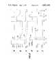
- FIG. 1is a simplified diagram in block and schematic form of a dc-to-dc converter in accordance with the invention, in which the control switch includes FETs in a bridge arrangement and which also includes a transformer coupled to receive drive from the FETs, and in which the current sense arrangement also includes a transformer:
- FIGS. 2a through 2f and 3a through 3cillustrate state-, voltage- or current-versus-time waveforms occurring in the arrangement of FIG. 1 during operation;
- FIG. 4illustrates another dc-to-dc converter in accordance with the invention in which a single controllable switch is used without a transformer, and in which the current sense arrangement includes a resistor;
- FIG. 5illustrates another dc-to-dc converter in accordance with the invention in which a pair of push-pull controllable switches are used in conjunction with a transformer, and in which the current sense circuit includes a resistor connected at one end to ground.
- FIG. 1illustrates a dc-to-dc converter in accordance with the invention.
- field-effect transistors 1, 2, 3 and 4are connected in a bridge arrangement.
- the main current-carrying source-to-drain paths of FETs 1 and 3are serially connected between a terminal 12 and ground with a node 14 therebetween, and the main current-carrying source-to-drain paths of FETs 2 and 4 are also serially connected between terminal 12 and ground, with a node 16 therebetween.
- a positive voltage +V1is applied to terminal 12 relative to ground.
- a primary winding 18' of a power transformer 18is connected between nodes 14 and 16 for receiving alternating voltage as a result of cyclical operation of switches 1-4.
- alternating voltage to primary winding 18' of transformer 18produces an alternating voltage across a secondary winding 18" which includes a center tap connected to a conductor 20.
- One end of secondary winding 18"is connected to the anode of a semiconductor rectifier 22, and the other end of secondary winding 18" is connected to the anode of a similar rectifier 24.
- the cathodes of rectifiers 22 and 24are connected together at a node 25, which is connected to one end of an inductor 26.
- a capacitor 30is connected between conductor 20 and the end of inductor 26 remote from node 25.
- a load or utilization apparatus illustrated as a resistor 32may be coupled across capacitor 30 by way of connectors 34, 34'.
- a pulsating direct voltagemeans a voltage which does not change polarity with respect to the reference, even though its magnitude may vary.
- the pulsating direct voltage at node 25 relative to conductor 20produces a current through inductor 26 having an average value, which current produces a direct voltage across capacitor 30 which may be used to energize load 32.
- a switch controller illustrated as a block 40is connected by conductors 6, 7, 8 and 9 to the gates of FETs 1, 2, 3 and 4, respectively, for, in pairs, controlling their operation in a cyclical manner.
- Controller 40receives synchronizing (sync) signals from a terminal 42 for synchronizing the cyclical operation of FETs 1-4, and also receives a current limit signal by way of a conductor 44 which is indicative of a current limit condition.
- Many types of switch mode operationare known. The operation of controller 40 as described in conjunction with FIGS. 2 and 3 is predicated upon operation in a current-programmed operating mode.
- FIG. 2aillustrates as a voltage-time waveform 242 the sync signal applied to terminal 42 of FIG. 1.
- One complete cycle of operationoccurs in the interval extending from time T0 to the next following time T0.
- Sync pulses 242make excursions to a logic HIGH condition beginning at recurrent times T0 and also beginning at recurrent times T10, midway between times T0.
- Sync signal 242is at a logic LOW level for a period of time preceding each excursion which begins at times T0 and T10.
- switch controller 40responds at a time T4 (i.e., after a delay from T3 to T4) by gating FETs 1 and 4 into conduction (an ON state), while maintaining FETs 2 and 3 in a nonconductive (OFF) state.
- T4i.e., after a delay from T3 to T4
- the delay between times T3 and T4is due to propagation delay in controller 40 and to the time required for charging the gate-to-source capacitance of the FETs being controlled from zero volts to their threshold voltages.
- the operating states of FETs 1 and 4is suggested in FIG. 2e by waveform 201, which represents the general magnitude of the current flow through FETs 1 and 4, and through primary winding 18' of transformer 18.
- waveform 202 of FIG. 2fsuggests the magnitude of the current through FETs 2 and 3, which is zero immediately before and after time T4.
- the current through each pair (1, 4; 2, 3) of FETs during their conductive periodsis a ramp of increasing magnitude with time.
- the ramp current 201 represented in FIG. 2eincreases from time T4 until switch controller 40 receives a signal on conductor 44 representative of a current magnitude limit.
- the current limit signaloccurs at a time T8.
- switch controller 40turns FETs 1 and 4 OFF.
- FETs 2 and 3remain OFF until a time T14 following the lagging edge of the next following sync pulse, which occurs at time T13. With both sets of FETs OFF in the interval T8-T14, no voltage is applied across primary winding 18' of transformer 18.
- FETs 2 and 3are turned ON to apply voltage across primary winding 18' with a polarity reversed from that applied during the interval T4-T8.
- a ramp current of increasing magnitudebegins to flow through FETs 2, 3 as illustrated by waveform 202 after time T14.
- the ramp of currentincreases until a later time T18 at which a current limit signal is applied over conductor 44 to switch controller 40.
- controller 40maintains FETs 1-4 nonconductive until the next following time T4, whereupon the cycle as described above begins again.
- Switch controllers such as 40are well known in the art and no further description is necessary.
- the primary winding 50' of a current transformer 50is serially connected with primary winding 18'.
- Current transformer 50includes a center-tapped secondary winding 50".
- the center tap of secondary winding 50"is connected to ground by way of a conductor 52.
- One end of secondary winding 50"is connected to the anode of a rectifier 54, the cathode of which is connected to a node 57.
- the other end of secondary winding 50"is connected to the anode of a rectifier 56, the cathode of which also is connected to node 57.
- a resistor 58is connected between node 57 and ground.
- the current-representative signal developed across resistor 58 of FIG. 1is coupled to the noninverting (+) input terminal of a comparator 46 by way of a resistor 49 and by a coupling arrangement designated generally as 60.
- Comparator 46compares that portion of the current-representative signal which is coupled to its +input terminal with a reference voltage (VREF) applied from a terminal 48 by way of a resistor 49' to the inverting (-) input terminal.
- VREFreference voltage
- comparator 46switches and produces a current limit signal on conductor 44 for application to switch controller 40.
- Coupling arrangement 60 of FIG. 1includes a switched voltage divider designated generally as 62 connected between node 57 and ground.
- Switched attenuator 62includes a first or series resistor 64, one end which is connected to node 57 and the other end of which is connected to a node 65.
- Voltage divider 62also includes as a shunt element the series combination of a second resistor 66 serially connected with the collector-to-emitter path of a bipolar NPN transistor 68 to form a switched resistor, which is connected between node 65 and ground.
- Coupling arrangement 60 of FIG. 1also includes a drive circuit designated generally as 70 for driving the base of transistor 68 in response to the sync signals applied to input terminal 42.
- Drive circuit 70includes a cascade of two inverting circuits 72, 74, together with their associated pull-up or collector resistors 76, 78.
- the output of inverting circuit 74is applied to the base of a bipolar NPN transistor 80, the emitter of which is connected by way of a node 82a and an oscillation suppression resistor 88a to a node 82.
- Resistors 76 and 78, and the collector of transistor 80are connected by a terminal 79 to a source +V2 of positive energizing voltage.
- Node 82is connected by way of a resistor 84 to a terminal 85 which is a source of negative energizing potential -V3.
- Node 82is also connected by way of a capacitor 86 to ground.
- Node 82is further connected by way of a resistor 88 and a node 69 to the base of transistor 68.
- the cathode of a diode 90is connected to node 69 and its anode is connected to ground.
- a further inverting circuit 92is connected to receive sync signal from input terminal 42, and its output is connected to node 69 and to the base of transistor 68.
- Inverting circuit 92has an "open collector output," and does not include a pull-up resistor, so its output is effectively open-circuited during those intervals during which its input signal has a logic LOW level.
- both rectifiers 22 and 24are capable of conducting in the reverse direction.
- a large spike of currentflows through the loop including secondary winding 18", rectifiers 22 and 24 and node 25, until the charge carriers are swept out in that one of rectifiers 22 and 24 which is reversed biased. That diode in which the charge carriers are swept out then becomes nonconductive, and the current spike ends.
- a current spikealso flows through primary winding 18'. The current spike is illustrated in FIG. 2e immediately after time T4, and in FIG. 2f immediately after time T14. The current spike is sensed by the current sense circuit including transformer 50 and resistor 58.
- a spike of the current sense signalappears at node 57 relative to ground immediately after times T4 and T14. If this spike is applied directly to the noninverting input terminal of comparator 46 by resistors 49 and 64, comparator 46 may switch, and switch controller 40 may undesirably turn OFF the associated FETs at a time unrelated to the magnitude of the ramp portion of the current flow through primary winding 18'.
- coupling circuit 60renders transistor 68 conductive for a predetermined interval bracketing (preceding, including and following) each of times T4 and T14, thereby causing resistor 64 to become part of voltage divider 62 which includes resistor 66.
- the current sense voltage at node 57is attenuated as it appears at node 65 for application by way of resistor 49 to the noninverting input of comparator 46.
- Resistor 49does not introduce further attenuation because of the high input impedance of the +input terminal of comparator 46.
- the attenuation introduced by voltage divider 62is such that the current spike does not cause comparator 46 to switch.
- diode 90 and transistors 68 and 80are silicon units with forward offset potentials of about 0.7 volts, and in which the important values are:
- coupling circuit 60is the same whether during the first half (times T0-T10) or the second half (times T10-T0) of an operating cycle. Operation will only be explained in the interval T0-T10, the remainder of the operation being understood therefrom.
- sync signal 242(FIG. 2 applied to sync input terminal 42 (FIG. 1) is at a logic LOW level, so the output voltage of inverting circuit 74 is also at a logic low level, and transistor 80, which is an emitter follower, sets node 82a at about -0.7 V.
- inverting circuit 92has an open-circuit output. As a result, conventional current flows from ground through diode 90, and through resistor 84a to the -V3 supply, resulting in -0.7 V at node 69. Resistors 88a and 88 are effectively in parallel at this time.
- the current sense signal voltageis applied substantially unattenuated from node 57 to the +input terminal of comparator 46 at times before time T0, as shown by state waveform 262 of FIG. 2d. Any current surge causing the current sense signal voltage as applied to the +input terminal of comparator 46 to exceed the VREF voltage at terminal 48 will switch comparator 46, resulting in shut-down of the converter.
- sync pulse 242(FIG. 2a) makes an excursion to a logic HIGH level, and remains at that level until time T3.
- sync pulse 242 HIGHthe open collector output of inverting circuit 74 is also logic HIGH or in the off state, and transistor 80 is rendered conductive as an emitter follower, with an output voltage of about 4.3 volts. This charges capacitor 86 toward +4.3 volts, as illustrated by waveform 286 of FIG. 2b in the interval T0-T2.
- inverting circuit 92With the sync pulse at a logic HIGH level, inverting circuit 92 is at a logic LOW level, thereby sinking current flowing through resistor 88 from node 82, thereby effectively setting the base of transistor 68 to zero volts, as illustrated in the interval T0-T3 in FIG. 2c. This renders diode 90 nonconductive, and also maintains the base-emitter junction of transistor 68 unbiased, and its collector at a high impedance. Voltage divider 62 continues to be disabled, so the current sense signal applied from node 57 to the +input of comparator 46 is not attenuated in the interval T0-T3, as illustrated by the UNATTEN condition of state waveform 262.
- sync pulse 242makes a transition from logic HIGH to a logic LOW level.
- Transistor 80(FIG. 1) becomes, nonconductive as its base-emitter junction becomes reverse-biased, and inverting circuit 92 assumes an open-collector condition.
- capacitor 86is charged to a voltage of +4.3 V, as illustrated by waveform 286 of FIG. 2b.
- capacitor 86progressively discharges through resistor 84 to terminal 85, and its voltage decreases until the value of -0.7 volts is ultimately reached.
- capacitor 86also discharges through resistor 88 and the base-emitter junction of transistor 58, thereby turning transistor 68 ON, thereby effectively grounding resistor 66 and enabling voltage divider 62 for attenuating the current sense signal voltage applied from node 57 to the + input terminal of comparator 46.
- a typical attenuationmay be 6 dB (i.e. 1/2).
- FIG. 3billustrates a magnitude-time waveform 310 representing the current through primary winding 18' and 50' of FIG. 1 during operation in a current-programmed mode, with sync pulses 242 re-illustrated in FIG. 3a for convenient reference.
- the ramps of currentare of decreasing duration, representing for example rapidly increasing input voltage concurrent with rapidly increasing load current.
- the ON times of switch pairs 1, 4; 2, 3increase.
- their conductive timescannot be allowed to reach 50% without the danger of damage due to the momentary formation of a direct path from voltage source 12 (FIG. 1) to ground.
- FIG. 3cillustrates a portion of FIG. 3b to an expanded time scale.
- the times (T8, T18) at which the ramp of current endsoccurs when the current magnitude reaches a limit value illustrated as dotted line 312.
- the effective current limit value in the intervals T3-T6, T13-T16is greater than that occurring during the remainder of each cycle, so that shut-down is not triggered even though the magnitude of the current spike in the intervals T3-T6, T13-T16 is greater than the magnitude of the ramp current required for temporary shut-off (at times T8, T18).
- coupling 60attenuates the current sense signal applied to comparator 46 for the intervals T3-T6 during each first half-cycle of operation, and equivalently for the interval T13-T16 in the second half-cycle. These intervals encompass the times during which a current surge occurs due to application of reverse voltage to semiconductor rectifiers which are momentarily rendered bidirectionally conductive by stored charge.
- the attenuationreduces the magnitude of the current sense signal applied to the comparator to a value which is less than the reference value, so that the current spike occurring due to normal operation will not trigger shut-down.
- a desirable attribute of the described arrangementis that a fault-related increase in magnitude of the current sense signal may nevertheless be sufficient to trigger shut-down even if it occurs during the period of attenuation.
- the current sense signalis applied in unattenuated form to the comparator, so that a fault may desirably result in shut-down even if the resulting current surge is smaller in magnitude than the current surge due to charge storage in the rectifiers.
- the path by which the current sense signal is coupled to the comparatoris not required to include low-pass filters which might undesirably introduce delay. As known, delay in feedback loops is undesirable and may even lead to instability.
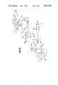
- FIG. 4illustrates an embodiment of the invention in simplified schematic form. Elements of FIG. 4 corresponding to those of FIG. 1 are designated by the same reference numerals, and elements having generally analogous functions are designated by the same reference numerals in the 400 series.
- inductor 26 and rectifier 428are connected at a node 414 with a FET switch 401 in the well known switched buck configuration.
- a resistor 450 connected between switch 401 and node 414generates a voltage which depends upon the magnitude of the current flow through switch 401.
- a differential amplifier 493performs a level-shifting function and may provide amplification to produce the current-representative signal voltage across a resistor 458, which is applied by a coupling 460 to the + input of comparator 46.
- Comparator 46compares the signal coupled to its + input with the reference voltage generated at terminal 48 to produce a current limit signal on conductor 44 and at the reset (R) input of a set-reset flip-flop (FF) 440.
- Sync pulses applied to an input terminal 42are coupled to the set (S) input of FF 440, and its output is coupled to the gate of FET 401.
- the sync pulsesets FF 440, which responds by gating FET 401 into conduction for causing an increasing ramp current through inductor 26.
- the ramp currentis integrated by capacitor 30 for generating voltage for load 30.
- comparator 46produces a current limit signal on conductor 44 which resets FF 440 to turn FET 401 OFF.
- Currentcontinues to flow through inductor 26, however, which causes "catch” or “free-wheeling” diode 428 to conduct, thereby resulting in storage of charge carriers therein.
- FET 401becomes conductive, a current surge occurs because diode 428 is momentarily a short-circuit during the interval in which the charge carriers are swept out. The current surge is attenuated during this interval by voltage divider 62 of coupling 460.
- Voltage divider 62includes controllable switch FET 468 controlled by a one-shot multivibrator (OS MVB) 499 which is triggered by sync applied to terminal 42.
- Multivibrator 499maintains FET 468 conductive for a period of time established by timing resistor 484 and timing capacitor 486. The period of time is selected to encompass the duration of the normal-operation current surge.
- FIG. 5is a simplified diagram in schematic and block form of another embodiment of the invention.
- elements corresponding to those of FIG. 1are designated by the same reference numbers, and elements with generally analogous functions are designated by the same reference numbers in the 500 series.
- transformer 518 with primary and secondary windings 518' and 518", respectivelyis identical to transformer 50 of FIG. 1, except that primary winding 518' has a center-tap.
- the center-tapis connected across a capacitor 599 to terminal 12. This allows push-pull operation by means of only two controllable switches, 501 and 502, which are illustrated as bipolar Darlingtons.
- Switch 501is connected to one end of primary winding 518', and switch 502 is connected to the other end.
- Both switches 501 and 502are connected together at a node point 598, which is coupled to ground by way of a low resistance current-sensing resistor 550.
- This type of connectionavoids the need for a level shifting circuit.
- An amplifier illustrated as 593has inputs connected across resistor 550, and couples amplified current sense signal by way of a resistor 64 to a switch control circuit 540.
- the arrangement of FIG. 5controls the series leg of a voltage divider including resistors 64 and 66.
- a resistor 597is coupled in parallel with resistor 64 by a controllable gate 568.
- Gate 568is controlled by the output of a set-reset latch 596 which is set at each sync pulse. The output also enables a gate 595 which couples clock signals from an oscillator 594 to a counter 591. Counter 591 resets latch 596 at a predetermined count to thereby close gates 595 and 568.
- controllable-gain amplifieralso known as an AGC amplifier
- operation of a current-programmed sourcehas been described, even voltage mode control loops with cycle-to-cycle current sensing for current-limiting may have the described problem, which may be solved in the same general manner as that described.
Landscapes
- Engineering & Computer Science (AREA)
- Power Engineering (AREA)
- Dc-Dc Converters (AREA)
Abstract
Description
______________________________________source +V2 +5 volts +V3 -5Resistor 76 2Kohms 782K 841K 84a 2.7K (also known as 2K7) 881K8 88a 39capacitor 86 680 picofarads______________________________________
Claims (12)
Priority Applications (1)
| Application Number | Priority Date | Filing Date | Title |
|---|---|---|---|
| US07/192,268US4811184A (en) | 1988-05-10 | 1988-05-10 | Switch-mode power supply with dynamic adjustment of current sense magnitude |
Applications Claiming Priority (1)
| Application Number | Priority Date | Filing Date | Title |
|---|---|---|---|
| US07/192,268US4811184A (en) | 1988-05-10 | 1988-05-10 | Switch-mode power supply with dynamic adjustment of current sense magnitude |
Publications (1)
| Publication Number | Publication Date |
|---|---|
| US4811184Atrue US4811184A (en) | 1989-03-07 |
Family
ID=22708969
Family Applications (1)
| Application Number | Title | Priority Date | Filing Date |
|---|---|---|---|
| US07/192,268Expired - Fee RelatedUS4811184A (en) | 1988-05-10 | 1988-05-10 | Switch-mode power supply with dynamic adjustment of current sense magnitude |
Country Status (1)
| Country | Link |
|---|---|
| US (1) | US4811184A (en) |
Cited By (40)
| Publication number | Priority date | Publication date | Assignee | Title |
|---|---|---|---|---|
| US4928220A (en)* | 1988-10-14 | 1990-05-22 | Compaq Computer Inc. | Switching mode DC-to-DC power supply with improved current sensing |
| US5157592A (en)* | 1991-10-15 | 1992-10-20 | International Business Machines Corporation | DC-DC converter with adaptive zero-voltage switching |
| EP0529366A1 (en)* | 1991-08-28 | 1993-03-03 | Siemens Aktiengesellschaft | Switching converter with current sensor |
| US5233287A (en)* | 1992-05-05 | 1993-08-03 | Space Systems/Loral | Current limiting bilateral converter having a ground referenced current sensor |
| US5399959A (en)* | 1991-11-14 | 1995-03-21 | Hilti Aktiengesellschaft | Circuit arrangement for contactless switchover of operation parameters of an electrically driven tool |
| US5399908A (en)* | 1992-06-26 | 1995-03-21 | Kollmorgen Corporation | Apparatus and method for forced sharing of parallel MOSFET switching losses |
| US5465201A (en)* | 1993-01-21 | 1995-11-07 | Lambda Electronics, Inc. | Overload protection of switch mode converters |
| US5600547A (en)* | 1994-12-21 | 1997-02-04 | Samsung Electro-Mechanics Co., Ltd. | Inverter circuit utilizing a frequency synchronization device |
| EP0809348A1 (en)* | 1996-05-21 | 1997-11-26 | Thomson-Csf | DC voltage switching power supply with current limitation |
| US5982639A (en)* | 1997-11-04 | 1999-11-09 | Power Integrations, Inc. | Two switch off-line switching converter |
| US6107851A (en)* | 1998-05-18 | 2000-08-22 | Power Integrations, Inc. | Offline converter with integrated softstart and frequency jitter |
| US6226190B1 (en) | 1998-02-27 | 2001-05-01 | Power Integrations, Inc. | Off-line converter with digital control |
| US6369559B1 (en)* | 2000-11-15 | 2002-04-09 | Texas Instruments Incorporated | Buck controller coprocessor to control switches |
| US6388430B1 (en) | 2001-09-13 | 2002-05-14 | The Esab Group, Inc. | Buck regulator circuit for use in a power supply |
| US6650558B1 (en) | 2002-05-06 | 2003-11-18 | Lockhead Martin Corporation | Asymmetrical drive circuit for full-wave bridge |
| US20030227730A1 (en)* | 2002-04-24 | 2003-12-11 | Junichi Iimura | Inverted circuit overcurrent protection device and hybrid integrated circuit device with the same incorporated |
| US20040183769A1 (en)* | 2000-09-08 | 2004-09-23 | Earl Schreyer | Graphics digitizer |
| US6876181B1 (en) | 1998-02-27 | 2005-04-05 | Power Integrations, Inc. | Off-line converter with digital control |
| US20060158166A1 (en)* | 2003-07-08 | 2006-07-20 | Roelf Van Der Wal | Method and device for sensing current |
| DE102005002359A1 (en)* | 2005-01-18 | 2006-07-27 | Puls Gmbh | Current limiting circuit and method of operating the circuit |
| US20070002512A1 (en)* | 2004-12-09 | 2007-01-04 | Puls Gmbh | Circuit arrangement for overvoltage detection and method for operating circuit arrangement |
| US20070047268A1 (en)* | 2005-08-26 | 2007-03-01 | Djenguerian Alex B | Method and apparatus for digital control of a switching regulator |
| US20080106917A1 (en)* | 2006-11-02 | 2008-05-08 | James Holt | Variable edge modulation in a switching regulator |
| US20080266738A1 (en)* | 2007-04-26 | 2008-10-30 | Polar Semiconductor, Inc. | Over-current protection device for a switched-mode power supply |
| US20090195229A1 (en)* | 2000-08-08 | 2009-08-06 | Power Integrations, Inc. | Method and apparatus for reducing audio noise in a switching regulator |
| US20100109617A1 (en)* | 2005-01-18 | 2010-05-06 | Puls Gmbh | Current-limiting circuit and method for operating the circuit |
| US7719243B1 (en) | 2007-11-21 | 2010-05-18 | Fairchild Semiconductor Corporation | Soft-start system and method for power converter |
| US7723972B1 (en) | 2008-03-19 | 2010-05-25 | Fairchild Semiconductor Corporation | Reducing soft start delay and providing soft recovery in power system controllers |
| US7872883B1 (en) | 2008-01-29 | 2011-01-18 | Fairchild Semiconductor Corporation | Synchronous buck power converter with free-running oscillator |
| US20110025281A1 (en)* | 2009-07-30 | 2011-02-03 | David Anthony Cross | Transient Differential Switching Regulator |
| US20110058285A1 (en)* | 2009-09-10 | 2011-03-10 | Polar Semiconductor, Inc. | Over-current protection device for a switched-mode power supply |
| US8018694B1 (en) | 2007-02-16 | 2011-09-13 | Fairchild Semiconductor Corporation | Over-current protection for a power converter |
| EP3074780A4 (en)* | 2012-11-23 | 2017-12-27 | Elevare Energy IP Pty Ltd | Electrical supply system |
| US9973084B2 (en) | 2014-11-20 | 2018-05-15 | Infineon Technologies Austria Ag | Switching voltage regulator input power estimation |
| US10069414B2 (en)* | 2015-04-01 | 2018-09-04 | Infineon Technologies Austria Ag | Switching voltage regulator input voltage and current sensing |
| US10224812B1 (en) | 2017-10-13 | 2019-03-05 | Infineon Technologies Austria Ag | Sensing network mismatch compensation for switching voltage regulator with input voltage and current sensing |
| US10389242B2 (en) | 2017-02-01 | 2019-08-20 | Infineon Technologies Austria Ag | Voltage and current sensing calibration for switching voltage regulators |
| US10610627B2 (en) | 2014-05-29 | 2020-04-07 | St. Vincent's Hospital Sydney Limited | Ventricular assist device method and apparatus |
| US12062910B2 (en) | 2019-09-09 | 2024-08-13 | Elexsis Pty Ltd | Two-way electrical power distribution network |
| US12401267B2 (en) | 2019-09-09 | 2025-08-26 | Elexsys Ip Pty Ltd | Electrical power regulating apparatus |
Citations (21)
| Publication number | Priority date | Publication date | Assignee | Title |
|---|---|---|---|---|
| US3859586A (en)* | 1973-09-26 | 1975-01-07 | Bell Telephone Labor Inc | Overcurrent protection circuit utilizing peak detection circuit with variable dynamic response |
| US4020423A (en)* | 1971-05-10 | 1977-04-26 | Carl Schenck Ag | Method and circuit arrangement for producing and transmitting electrical reference pulses |
| US4069452A (en)* | 1976-09-15 | 1978-01-17 | Dana Laboratories, Inc. | Apparatus for automatically detecting values of periodically time varying signals |
| US4109198A (en)* | 1975-09-08 | 1978-08-22 | Victor Company Of Japan, Limited | Peak level indicating electronic circuit |
| US4121121A (en)* | 1977-09-13 | 1978-10-17 | Computer Identics Corporation | Follower response control circuit |
| US4144544A (en)* | 1977-12-19 | 1979-03-13 | Rca Corporation | Television horizontal oscillator frequency control arrangement for use with tape recorder |
| US4144545A (en)* | 1977-12-19 | 1979-03-13 | Rca Corporation | Television horizontal oscillator frequency control arrangement for use with a tape recorder |
| US4163909A (en)* | 1977-08-23 | 1979-08-07 | International Business Machines Corporation | Peak detecting circuitry and dual threshold circuitry therefor |
| US4282014A (en)* | 1975-01-31 | 1981-08-04 | Siemens Aktiengesellschaft | Detector for detecting voltage breakdowns on the high-voltage side of an electric precipitator |
| US4392103A (en)* | 1980-06-10 | 1983-07-05 | Organisation Europeenne De Recherches Spatiales | Current sensing regulator |
| US4399414A (en)* | 1981-06-16 | 1983-08-16 | Bird David A | Low-noise pulse conditioner |
| US4423457A (en)* | 1981-02-05 | 1983-12-27 | Siemens Aktiengesellschaft | Overload protection circuit for a semiconductor switch |
| US4453193A (en)* | 1982-10-12 | 1984-06-05 | General Electric Company | Overcurrent protection for push-pull circuits |
| US4524412A (en)* | 1983-06-06 | 1985-06-18 | At&T Bell Laboratories | Peak current controlled converter with additional current threshold control level to limit current tailout during overload conditions |
| US4569009A (en)* | 1984-03-05 | 1986-02-04 | Honeywell Information Systems Inc. | Switching regulator having a selectable gain amplifier for providing a selectively alterable output voltage |
| US4586120A (en)* | 1983-12-30 | 1986-04-29 | At&T Bell Laboratories | Current limit shutdown circuit with time delay |
| US4616301A (en)* | 1984-04-30 | 1986-10-07 | Boschert Inc. | Regulator control system |
| US4626979A (en)* | 1985-02-22 | 1986-12-02 | Diego Power | Anticipatory feedback technique for pulse width modulated power supply |
| US4686617A (en)* | 1986-06-06 | 1987-08-11 | Rca Corporation | Current limited constant frequency dc converter |
| US4725769A (en)* | 1986-04-22 | 1988-02-16 | Sgs Microelettronica S.P.A. | Current limited for constant current for switching driving devices |
| JPH10516A (en)* | 1996-06-10 | 1998-01-06 | Hideo Nakagawa | Snap ring fitting device |
- 1988
- 1988-05-10USUS07/192,268patent/US4811184A/ennot_activeExpired - Fee Related
Patent Citations (21)
| Publication number | Priority date | Publication date | Assignee | Title |
|---|---|---|---|---|
| US4020423A (en)* | 1971-05-10 | 1977-04-26 | Carl Schenck Ag | Method and circuit arrangement for producing and transmitting electrical reference pulses |
| US3859586A (en)* | 1973-09-26 | 1975-01-07 | Bell Telephone Labor Inc | Overcurrent protection circuit utilizing peak detection circuit with variable dynamic response |
| US4282014A (en)* | 1975-01-31 | 1981-08-04 | Siemens Aktiengesellschaft | Detector for detecting voltage breakdowns on the high-voltage side of an electric precipitator |
| US4109198A (en)* | 1975-09-08 | 1978-08-22 | Victor Company Of Japan, Limited | Peak level indicating electronic circuit |
| US4069452A (en)* | 1976-09-15 | 1978-01-17 | Dana Laboratories, Inc. | Apparatus for automatically detecting values of periodically time varying signals |
| US4163909A (en)* | 1977-08-23 | 1979-08-07 | International Business Machines Corporation | Peak detecting circuitry and dual threshold circuitry therefor |
| US4121121A (en)* | 1977-09-13 | 1978-10-17 | Computer Identics Corporation | Follower response control circuit |
| US4144544A (en)* | 1977-12-19 | 1979-03-13 | Rca Corporation | Television horizontal oscillator frequency control arrangement for use with tape recorder |
| US4144545A (en)* | 1977-12-19 | 1979-03-13 | Rca Corporation | Television horizontal oscillator frequency control arrangement for use with a tape recorder |
| US4392103A (en)* | 1980-06-10 | 1983-07-05 | Organisation Europeenne De Recherches Spatiales | Current sensing regulator |
| US4423457A (en)* | 1981-02-05 | 1983-12-27 | Siemens Aktiengesellschaft | Overload protection circuit for a semiconductor switch |
| US4399414A (en)* | 1981-06-16 | 1983-08-16 | Bird David A | Low-noise pulse conditioner |
| US4453193A (en)* | 1982-10-12 | 1984-06-05 | General Electric Company | Overcurrent protection for push-pull circuits |
| US4524412A (en)* | 1983-06-06 | 1985-06-18 | At&T Bell Laboratories | Peak current controlled converter with additional current threshold control level to limit current tailout during overload conditions |
| US4586120A (en)* | 1983-12-30 | 1986-04-29 | At&T Bell Laboratories | Current limit shutdown circuit with time delay |
| US4569009A (en)* | 1984-03-05 | 1986-02-04 | Honeywell Information Systems Inc. | Switching regulator having a selectable gain amplifier for providing a selectively alterable output voltage |
| US4616301A (en)* | 1984-04-30 | 1986-10-07 | Boschert Inc. | Regulator control system |
| US4626979A (en)* | 1985-02-22 | 1986-12-02 | Diego Power | Anticipatory feedback technique for pulse width modulated power supply |
| US4725769A (en)* | 1986-04-22 | 1988-02-16 | Sgs Microelettronica S.P.A. | Current limited for constant current for switching driving devices |
| US4686617A (en)* | 1986-06-06 | 1987-08-11 | Rca Corporation | Current limited constant frequency dc converter |
| JPH10516A (en)* | 1996-06-10 | 1998-01-06 | Hideo Nakagawa | Snap ring fitting device |
Non-Patent Citations (3)
| Title |
|---|
| "Modelling and Analysis of Switching DC-to-DC Converters in Constant-Frequency Current-Programmed Moe" by HSU et al., published 1979 by IEEE; pp. 284-301. |
| Modelling and Analysis of Switching DC to DC Converters in Constant Frequency Current Programmed Moe by HSU et al., published 1979 by IEEE; pp. 284 301.* |
| Mumaw, Programmable Regulator Card, IBM Tech. Discl. Bul., vol. 20, No. 6, p. 2180, Nov. 1977.* |
Cited By (81)
| Publication number | Priority date | Publication date | Assignee | Title |
|---|---|---|---|---|
| US4928220A (en)* | 1988-10-14 | 1990-05-22 | Compaq Computer Inc. | Switching mode DC-to-DC power supply with improved current sensing |
| EP0529366A1 (en)* | 1991-08-28 | 1993-03-03 | Siemens Aktiengesellschaft | Switching converter with current sensor |
| US5157592A (en)* | 1991-10-15 | 1992-10-20 | International Business Machines Corporation | DC-DC converter with adaptive zero-voltage switching |
| US5399959A (en)* | 1991-11-14 | 1995-03-21 | Hilti Aktiengesellschaft | Circuit arrangement for contactless switchover of operation parameters of an electrically driven tool |
| US5233287A (en)* | 1992-05-05 | 1993-08-03 | Space Systems/Loral | Current limiting bilateral converter having a ground referenced current sensor |
| US5399908A (en)* | 1992-06-26 | 1995-03-21 | Kollmorgen Corporation | Apparatus and method for forced sharing of parallel MOSFET switching losses |
| US5465201A (en)* | 1993-01-21 | 1995-11-07 | Lambda Electronics, Inc. | Overload protection of switch mode converters |
| US5600547A (en)* | 1994-12-21 | 1997-02-04 | Samsung Electro-Mechanics Co., Ltd. | Inverter circuit utilizing a frequency synchronization device |
| EP0809348A1 (en)* | 1996-05-21 | 1997-11-26 | Thomson-Csf | DC voltage switching power supply with current limitation |
| FR2749110A1 (en)* | 1996-05-21 | 1997-11-28 | Thomson Csf | CONTINUOUS POWER SUPPLY WITH CURRENT CURRENT LIMITATION |
| US5982639A (en)* | 1997-11-04 | 1999-11-09 | Power Integrations, Inc. | Two switch off-line switching converter |
| US6005781A (en)* | 1997-11-04 | 1999-12-21 | Power Integrations, Inc. | Two switch off-line switching converter |
| US7477534B2 (en) | 1998-02-27 | 2009-01-13 | Power Integrations, Inc. | Off-line converter with digital control |
| US6608471B2 (en) | 1998-02-27 | 2003-08-19 | Power Integrations, Inc. | Off-line converter with digital control |
| US20060192540A1 (en)* | 1998-02-27 | 2006-08-31 | Balu Balakrishnan | Off-line converter with digital control |
| US6297623B1 (en) | 1998-02-27 | 2001-10-02 | Power Integrations, Inc. | Off-line converter with digital control |
| US7974112B2 (en) | 1998-02-27 | 2011-07-05 | Power Integrations, Inc. | Off-line converter with digital control |
| US20090091309A1 (en)* | 1998-02-27 | 2009-04-09 | Power Integrations, Inc. | Off-line converter with digital control |
| US6414471B1 (en) | 1998-02-27 | 2002-07-02 | Power Integrations, Inc. | Off-line converter with digital control |
| US6226190B1 (en) | 1998-02-27 | 2001-05-01 | Power Integrations, Inc. | Off-line converter with digital control |
| US8248053B2 (en) | 1998-02-27 | 2012-08-21 | Power Integrations, Inc. | Off-line converter with digital control |
| US7248029B2 (en) | 1998-02-27 | 2007-07-24 | Power Integrations, Inc. | Off-line converter with digital control |
| US20040017182A1 (en)* | 1998-02-27 | 2004-01-29 | Balu Balakrishnan | Off-line converter with digital control |
| US6747444B2 (en) | 1998-02-27 | 2004-06-08 | Power Integrations, Inc. | Off-line converter with digital control |
| US8710817B2 (en) | 1998-02-27 | 2014-04-29 | Power Integrations, Inc. | Off-line converter with digital control |
| US6876181B1 (en) | 1998-02-27 | 2005-04-05 | Power Integrations, Inc. | Off-line converter with digital control |
| US20050146314A1 (en)* | 1998-02-27 | 2005-07-07 | Balu Balakrishnan | Off-line converter with digital control |
| US7038439B2 (en) | 1998-02-27 | 2006-05-02 | Power Integrations, Inc. | Off-line converter with digital control |
| US6107851A (en)* | 1998-05-18 | 2000-08-22 | Power Integrations, Inc. | Offline converter with integrated softstart and frequency jitter |
| US6229366B1 (en) | 1998-05-18 | 2001-05-08 | Power Integrations, Inc. | Off-line converter with integrated softstart and frequency jitter |
| US7701186B2 (en) | 2000-08-08 | 2010-04-20 | Power Integrations, Inc. | Method and apparatus for reducing audio noise in a switching regulator |
| US20090195229A1 (en)* | 2000-08-08 | 2009-08-06 | Power Integrations, Inc. | Method and apparatus for reducing audio noise in a switching regulator |
| US20040183769A1 (en)* | 2000-09-08 | 2004-09-23 | Earl Schreyer | Graphics digitizer |
| US6369559B1 (en)* | 2000-11-15 | 2002-04-09 | Texas Instruments Incorporated | Buck controller coprocessor to control switches |
| US6388430B1 (en) | 2001-09-13 | 2002-05-14 | The Esab Group, Inc. | Buck regulator circuit for use in a power supply |
| US7136269B2 (en)* | 2002-04-24 | 2006-11-14 | Sanyo Electric Co., Ltd. | Inverted circuit overcurrent protection device and hybrid integrated circuit device with the same incorporated |
| US20070014065A1 (en)* | 2002-04-24 | 2007-01-18 | Sanyo Electric Co., Ltd. | Inverted circuit overcurrent protection device and hybrid integrated circuit device with the same incorporated |
| US20030227730A1 (en)* | 2002-04-24 | 2003-12-11 | Junichi Iimura | Inverted circuit overcurrent protection device and hybrid integrated circuit device with the same incorporated |
| US7609498B2 (en) | 2002-04-24 | 2009-10-27 | Sanyo Electric Co., Ltd. | Inverted circuit overcurrent protection device and hybrid integrated circuit device with the same incorporated |
| US6650558B1 (en) | 2002-05-06 | 2003-11-18 | Lockhead Martin Corporation | Asymmetrical drive circuit for full-wave bridge |
| US7521910B2 (en)* | 2003-07-08 | 2009-04-21 | Koninklijke Philips Electronics N.V. | Method and device for measuring current in a switched current path of a circuit |
| US20060158166A1 (en)* | 2003-07-08 | 2006-07-20 | Roelf Van Der Wal | Method and device for sensing current |
| US20070002512A1 (en)* | 2004-12-09 | 2007-01-04 | Puls Gmbh | Circuit arrangement for overvoltage detection and method for operating circuit arrangement |
| DE102005002359A1 (en)* | 2005-01-18 | 2006-07-27 | Puls Gmbh | Current limiting circuit and method of operating the circuit |
| US7852051B2 (en) | 2005-01-18 | 2010-12-14 | Puls Gmbh | Current-limiting circuit and method for operating the circuit |
| DE102005002359C5 (en)* | 2005-01-18 | 2015-10-29 | Puls Gmbh | Current limiting circuit and method of operating the circuit |
| DE102005002359B4 (en)* | 2005-01-18 | 2009-12-31 | Puls Gmbh | Current limiting circuit and method of operating the circuit |
| US20060164776A1 (en)* | 2005-01-18 | 2006-07-27 | Puls Gmbh | Current-limiting circuit and method for operating the circuit |
| US20100109617A1 (en)* | 2005-01-18 | 2010-05-06 | Puls Gmbh | Current-limiting circuit and method for operating the circuit |
| US8194422B2 (en) | 2005-08-26 | 2012-06-05 | Power Integrations, Inc. | Method and apparatus for digital control of a switching regulator |
| US7755917B2 (en) | 2005-08-26 | 2010-07-13 | Power Integrations, Inc. | Modulation of a feedback signal used in a digital control of a switching regulator |
| US20070047268A1 (en)* | 2005-08-26 | 2007-03-01 | Djenguerian Alex B | Method and apparatus for digital control of a switching regulator |
| US7830678B2 (en) | 2005-08-26 | 2010-11-09 | Power Integrations, Inc. | Method and apparatus for digital control of a switching regulator |
| US7233504B2 (en) | 2005-08-26 | 2007-06-19 | Power Integration, Inc. | Method and apparatus for digital control of a switching regulator |
| US8654547B2 (en) | 2005-08-26 | 2014-02-18 | Power Integrations, Inc. | Method and apparatus for digital control of a switching regulator |
| US10224820B2 (en) | 2005-08-26 | 2019-03-05 | Power Integrations, Inc. | Method and apparatus for digital control of a switching regulator |
| US20070217232A1 (en)* | 2005-08-26 | 2007-09-20 | Djenguerian Alex B | Method and apparatus for digital control of a switching regulator |
| US9484824B2 (en) | 2005-08-26 | 2016-11-01 | Power Integrations, Inc. | Method and apparatus for digital control of a switching regulator |
| US20080106917A1 (en)* | 2006-11-02 | 2008-05-08 | James Holt | Variable edge modulation in a switching regulator |
| US8018694B1 (en) | 2007-02-16 | 2011-09-13 | Fairchild Semiconductor Corporation | Over-current protection for a power converter |
| US20080266738A1 (en)* | 2007-04-26 | 2008-10-30 | Polar Semiconductor, Inc. | Over-current protection device for a switched-mode power supply |
| US7817391B2 (en) | 2007-04-26 | 2010-10-19 | Polar Semiconductor, Inc. | Over-current protection device for a switched-mode power supply |
| US7719243B1 (en) | 2007-11-21 | 2010-05-18 | Fairchild Semiconductor Corporation | Soft-start system and method for power converter |
| US7872883B1 (en) | 2008-01-29 | 2011-01-18 | Fairchild Semiconductor Corporation | Synchronous buck power converter with free-running oscillator |
| US7723972B1 (en) | 2008-03-19 | 2010-05-25 | Fairchild Semiconductor Corporation | Reducing soft start delay and providing soft recovery in power system controllers |
| US20110025281A1 (en)* | 2009-07-30 | 2011-02-03 | David Anthony Cross | Transient Differential Switching Regulator |
| GB2473598B (en)* | 2009-07-30 | 2013-03-06 | Pulse Electronics Avionics Ltd | Transient differential switching regulator |
| US8466668B2 (en) | 2009-07-30 | 2013-06-18 | Pulse Electronics (Avionics) Limited | Transient differential switching regulator |
| US20110058285A1 (en)* | 2009-09-10 | 2011-03-10 | Polar Semiconductor, Inc. | Over-current protection device for a switched-mode power supply |
| US8385029B2 (en) | 2009-09-10 | 2013-02-26 | Polar Semiconductor, Inc. | Over-current protection device for a switched-mode power supply |
| EP3074780A4 (en)* | 2012-11-23 | 2017-12-27 | Elevare Energy IP Pty Ltd | Electrical supply system |
| US10338121B2 (en) | 2012-11-23 | 2019-07-02 | Elevare Energy Ip Pty Ltd | Electrical supply system |
| US10884071B2 (en) | 2012-11-23 | 2021-01-05 | Elexsys IP Pty Ltd. | Electrical supply system |
| US10610627B2 (en) | 2014-05-29 | 2020-04-07 | St. Vincent's Hospital Sydney Limited | Ventricular assist device method and apparatus |
| US9973084B2 (en) | 2014-11-20 | 2018-05-15 | Infineon Technologies Austria Ag | Switching voltage regulator input power estimation |
| US10069414B2 (en)* | 2015-04-01 | 2018-09-04 | Infineon Technologies Austria Ag | Switching voltage regulator input voltage and current sensing |
| US10389242B2 (en) | 2017-02-01 | 2019-08-20 | Infineon Technologies Austria Ag | Voltage and current sensing calibration for switching voltage regulators |
| US10608537B2 (en) | 2017-02-01 | 2020-03-31 | Infineon Technologies Austria Ag | Input calibration for switching voltage regulators |
| US10224812B1 (en) | 2017-10-13 | 2019-03-05 | Infineon Technologies Austria Ag | Sensing network mismatch compensation for switching voltage regulator with input voltage and current sensing |
| US12062910B2 (en) | 2019-09-09 | 2024-08-13 | Elexsis Pty Ltd | Two-way electrical power distribution network |
| US12401267B2 (en) | 2019-09-09 | 2025-08-26 | Elexsys Ip Pty Ltd | Electrical power regulating apparatus |
Similar Documents
| Publication | Publication Date | Title |
|---|---|---|
| US4811184A (en) | Switch-mode power supply with dynamic adjustment of current sense magnitude | |
| US4686617A (en) | Current limited constant frequency dc converter | |
| EP0385546B1 (en) | Switched-mode power supply circuit including a starting circuit | |
| CA1288474C (en) | Power converter with reduced switching loss | |
| CA1278339C (en) | Inductor current control circuit | |
| US3989995A (en) | Frequency stabilized single-ended regulated converter circuit | |
| US4937727A (en) | Switch-mode power supply with transformer-coupled feedback | |
| US4618812A (en) | Direct current power control on selectable voltage step-up and step-down | |
| US4533836A (en) | Multiple voltage switching power supply having output voltage limiting | |
| US4805081A (en) | Multi-mode control systems for high-frequency resonant inverters | |
| JPH0697841B2 (en) | Power switching circuit | |
| JP4460105B2 (en) | Soft switching regulator type power supply device and output adjustment method thereof | |
| JPS5924442B2 (en) | Pulse width modulation voltage regulator converter and power converter | |
| US5570277A (en) | Switching power supply apparatus | |
| US5517397A (en) | Flyback power converter with spike compensator circuit | |
| US4688161A (en) | Regulated power supply apparatus and method using reverse phase angle control | |
| NZ209570A (en) | Switching regulator | |
| US4334184A (en) | Electronic sensor on/off switch | |
| US4885673A (en) | Demagnetization monitoring device for a switching power supply with a primary and a secondary regulation | |
| US4176304A (en) | Regulating television horizontal deflection arrangement | |
| JP4339129B2 (en) | Switch mode power supply | |
| JPS6239591B2 (en) | ||
| JPS62285665A (en) | Changeover type electric source unit | |
| JP3305317B2 (en) | Switch mode power supply with reduced input current distortion | |
| US5708577A (en) | Regulated power supply |
Legal Events
| Date | Code | Title | Description |
|---|---|---|---|
| AS | Assignment | Owner name:GENERAL ELECTRIC COMPANY A CORP. OF NEW YORK Free format text:ASSIGNMENT OF ASSIGNORS INTEREST.;ASSIGNORS:KONINSKY, PETER M.;D'ARIANO, EMILIO F.;REEL/FRAME:004889/0195;SIGNING DATES FROM 19880503 TO 19880506 Owner name:GENERAL ELECTRIC COMPANY, NEW YORK Free format text:ASSIGNMENT OF ASSIGNORS INTEREST;ASSIGNORS:KONINSKY, PETER M.;D'ARIANO, EMILIO F.;SIGNING DATES FROM 19880503 TO 19880506;REEL/FRAME:004889/0195 | |
| FPAY | Fee payment | Year of fee payment:4 | |
| FEPP | Fee payment procedure | Free format text:PAYOR NUMBER ASSIGNED (ORIGINAL EVENT CODE: ASPN); ENTITY STATUS OF PATENT OWNER: LARGE ENTITY | |
| AS | Assignment | Owner name:MARTIN MARIETTA CORPORATION, MARYLAND Free format text:ASSIGNMENT OF ASSIGNORS INTEREST;ASSIGNOR:GENERAL ELECTRIC COMPANY;REEL/FRAME:007046/0736 Effective date:19940322 | |
| REMI | Maintenance fee reminder mailed | ||
| LAPS | Lapse for failure to pay maintenance fees | ||
| FP | Lapsed due to failure to pay maintenance fee | Effective date:19970312 | |
| AS | Assignment | Owner name:LOCKHEED MARTIN CORPORATION, MARYLAND Free format text:ASSIGNMENT OF ASSIGNORS INTEREST;ASSIGNOR:MARTIN MARIETTA CORPORATION;REEL/FRAME:008628/0518 Effective date:19960128 | |
| FEPP | Fee payment procedure | Free format text:PAYER NUMBER DE-ASSIGNED (ORIGINAL EVENT CODE: RMPN); ENTITY STATUS OF PATENT OWNER: LARGE ENTITY Free format text:PAYOR NUMBER ASSIGNED (ORIGINAL EVENT CODE: ASPN); ENTITY STATUS OF PATENT OWNER: LARGE ENTITY | |
| STCH | Information on status: patent discontinuation | Free format text:PATENT EXPIRED DUE TO NONPAYMENT OF MAINTENANCE FEES UNDER 37 CFR 1.362 |