US4811081A - Semiconductor die bonding with conductive adhesive - Google Patents
Semiconductor die bonding with conductive adhesiveDownload PDFInfo
- Publication number
- US4811081A US4811081AUS07/029,294US2929487AUS4811081AUS 4811081 AUS4811081 AUS 4811081AUS 2929487 AUS2929487 AUS 2929487AUS 4811081 AUS4811081 AUS 4811081A
- Authority
- US
- United States
- Prior art keywords
- die
- conductive
- tape
- substrate
- semiconductor
- Prior art date
- Legal status (The legal status is an assumption and is not a legal conclusion. Google has not performed a legal analysis and makes no representation as to the accuracy of the status listed.)
- Expired - Lifetime
Links
- 239000000853adhesiveSubstances0.000titleclaimsabstractdescription42
- 230000001070adhesive effectEffects0.000titleclaimsabstractdescription42
- 239000004065semiconductorSubstances0.000titleclaimsabstractdescription37
- 239000000758substrateSubstances0.000claimsabstractdescription43
- 239000004020conductorSubstances0.000claimsabstractdescription28
- 238000012360testing methodMethods0.000claimsdescription24
- 238000000034methodMethods0.000claimsdescription11
- 230000008569processEffects0.000claimsdescription7
- 239000000523sampleSubstances0.000abstractdescription6
- 230000002950deficientEffects0.000description7
- 239000000969carrierSubstances0.000description6
- 230000008901benefitEffects0.000description4
- 229910052751metalInorganic materials0.000description4
- 239000002184metalSubstances0.000description4
- 239000010408filmSubstances0.000description3
- 229910052782aluminiumInorganic materials0.000description2
- 230000013011matingEffects0.000description2
- 229920003223poly(pyromellitimide-1,4-diphenyl ether)Polymers0.000description2
- 230000005855radiationEffects0.000description2
- 229920002799BoPETPolymers0.000description1
- RYGMFSIKBFXOCR-UHFFFAOYSA-NCopperChemical compound[Cu]RYGMFSIKBFXOCR-UHFFFAOYSA-N0.000description1
- 239000004593EpoxySubstances0.000description1
- 239000005041Mylar™Substances0.000description1
- 230000004075alterationEffects0.000description1
- XAGFODPZIPBFFR-UHFFFAOYSA-NaluminiumChemical compound[Al]XAGFODPZIPBFFR-UHFFFAOYSA-N0.000description1
- 239000000919ceramicSubstances0.000description1
- 229920001940conductive polymerPolymers0.000description1
- 238000011109contaminationMethods0.000description1
- 238000007796conventional methodMethods0.000description1
- 229910052802copperInorganic materials0.000description1
- 239000010949copperSubstances0.000description1
- 230000007547defectEffects0.000description1
- 230000007812deficiencyEffects0.000description1
- 230000007613environmental effectEffects0.000description1
- 239000011888foilSubstances0.000description1
- PCHJSUWPFVWCPO-UHFFFAOYSA-NgoldChemical compound[Au]PCHJSUWPFVWCPO-UHFFFAOYSA-N0.000description1
- 239000010931goldSubstances0.000description1
- 229910052737goldInorganic materials0.000description1
- 238000010438heat treatmentMethods0.000description1
- 238000010030laminatingMethods0.000description1
- 239000007788liquidSubstances0.000description1
- 239000000463materialSubstances0.000description1
- 238000012986modificationMethods0.000description1
- 230000004048modificationEffects0.000description1
- 239000002245particleSubstances0.000description1
- 238000001259photo etchingMethods0.000description1
- 238000004382pottingMethods0.000description1
- 238000012545processingMethods0.000description1
- 239000000565sealantSubstances0.000description1
- 238000007789sealingMethods0.000description1
- 238000000926separation methodMethods0.000description1
- 229910000679solderInorganic materials0.000description1
- 238000004544sputter depositionMethods0.000description1
- 239000010409thin filmSubstances0.000description1
- MAKDTFFYCIMFQP-UHFFFAOYSA-Ntitanium tungstenChemical compound[Ti].[W]MAKDTFFYCIMFQP-UHFFFAOYSA-N0.000description1
Images


Classifications
- H—ELECTRICITY
- H01—ELECTRIC ELEMENTS
- H01L—SEMICONDUCTOR DEVICES NOT COVERED BY CLASS H10
- H01L24/00—Arrangements for connecting or disconnecting semiconductor or solid-state bodies; Methods or apparatus related thereto
- H01L24/80—Methods for connecting semiconductor or other solid state bodies using means for bonding being attached to, or being formed on, the surface to be connected
- H01L24/81—Methods for connecting semiconductor or other solid state bodies using means for bonding being attached to, or being formed on, the surface to be connected using a bump connector
- H—ELECTRICITY
- H01—ELECTRIC ELEMENTS
- H01L—SEMICONDUCTOR DEVICES NOT COVERED BY CLASS H10
- H01L21/00—Processes or apparatus adapted for the manufacture or treatment of semiconductor or solid state devices or of parts thereof
- H01L21/02—Manufacture or treatment of semiconductor devices or of parts thereof
- H01L21/04—Manufacture or treatment of semiconductor devices or of parts thereof the devices having potential barriers, e.g. a PN junction, depletion layer or carrier concentration layer
- H01L21/50—Assembly of semiconductor devices using processes or apparatus not provided for in a single one of the groups H01L21/18 - H01L21/326 or H10D48/04 - H10D48/07 e.g. sealing of a cap to a base of a container
- H01L21/56—Encapsulations, e.g. encapsulation layers, coatings
- H01L21/563—Encapsulation of active face of flip-chip device, e.g. underfilling or underencapsulation of flip-chip, encapsulation preform on chip or mounting substrate
- H—ELECTRICITY
- H01—ELECTRIC ELEMENTS
- H01L—SEMICONDUCTOR DEVICES NOT COVERED BY CLASS H10
- H01L23/00—Details of semiconductor or other solid state devices
- H01L23/48—Arrangements for conducting electric current to or from the solid state body in operation, e.g. leads, terminal arrangements ; Selection of materials therefor
- H01L23/482—Arrangements for conducting electric current to or from the solid state body in operation, e.g. leads, terminal arrangements ; Selection of materials therefor consisting of lead-in layers inseparably applied to the semiconductor body (electrodes)
- H01L23/4827—Materials
- H01L23/4828—Conductive organic material or pastes, e.g. conductive adhesives, inks
- H—ELECTRICITY
- H01—ELECTRIC ELEMENTS
- H01L—SEMICONDUCTOR DEVICES NOT COVERED BY CLASS H10
- H01L23/00—Details of semiconductor or other solid state devices
- H01L23/48—Arrangements for conducting electric current to or from the solid state body in operation, e.g. leads, terminal arrangements ; Selection of materials therefor
- H01L23/488—Arrangements for conducting electric current to or from the solid state body in operation, e.g. leads, terminal arrangements ; Selection of materials therefor consisting of soldered or bonded constructions
- H01L23/498—Leads, i.e. metallisations or lead-frames on insulating substrates, e.g. chip carriers
- H01L23/49866—Leads, i.e. metallisations or lead-frames on insulating substrates, e.g. chip carriers characterised by the materials
- H01L23/49883—Leads, i.e. metallisations or lead-frames on insulating substrates, e.g. chip carriers characterised by the materials the conductive materials containing organic materials or pastes, e.g. for thick films
- H—ELECTRICITY
- H01—ELECTRIC ELEMENTS
- H01L—SEMICONDUCTOR DEVICES NOT COVERED BY CLASS H10
- H01L24/00—Arrangements for connecting or disconnecting semiconductor or solid-state bodies; Methods or apparatus related thereto
- H01L24/01—Means for bonding being attached to, or being formed on, the surface to be connected, e.g. chip-to-package, die-attach, "first-level" interconnects; Manufacturing methods related thereto
- H01L24/50—Tape automated bonding [TAB] connectors, i.e. film carriers; Manufacturing methods related thereto
- H—ELECTRICITY
- H01—ELECTRIC ELEMENTS
- H01L—SEMICONDUCTOR DEVICES NOT COVERED BY CLASS H10
- H01L24/00—Arrangements for connecting or disconnecting semiconductor or solid-state bodies; Methods or apparatus related thereto
- H01L24/80—Methods for connecting semiconductor or other solid state bodies using means for bonding being attached to, or being formed on, the surface to be connected
- H01L24/83—Methods for connecting semiconductor or other solid state bodies using means for bonding being attached to, or being formed on, the surface to be connected using a layer connector
- H—ELECTRICITY
- H01—ELECTRIC ELEMENTS
- H01L—SEMICONDUCTOR DEVICES NOT COVERED BY CLASS H10
- H01L24/00—Arrangements for connecting or disconnecting semiconductor or solid-state bodies; Methods or apparatus related thereto
- H01L24/80—Methods for connecting semiconductor or other solid state bodies using means for bonding being attached to, or being formed on, the surface to be connected
- H01L24/86—Methods for connecting semiconductor or other solid state bodies using means for bonding being attached to, or being formed on, the surface to be connected using tape automated bonding [TAB]
- H—ELECTRICITY
- H01—ELECTRIC ELEMENTS
- H01L—SEMICONDUCTOR DEVICES NOT COVERED BY CLASS H10
- H01L2224/00—Indexing scheme for arrangements for connecting or disconnecting semiconductor or solid-state bodies and methods related thereto as covered by H01L24/00
- H01L2224/01—Means for bonding being attached to, or being formed on, the surface to be connected, e.g. chip-to-package, die-attach, "first-level" interconnects; Manufacturing methods related thereto
- H01L2224/10—Bump connectors; Manufacturing methods related thereto
- H01L2224/15—Structure, shape, material or disposition of the bump connectors after the connecting process
- H01L2224/16—Structure, shape, material or disposition of the bump connectors after the connecting process of an individual bump connector
- H01L2224/161—Disposition
- H01L2224/16151—Disposition the bump connector connecting between a semiconductor or solid-state body and an item not being a semiconductor or solid-state body, e.g. chip-to-substrate, chip-to-passive
- H01L2224/16221—Disposition the bump connector connecting between a semiconductor or solid-state body and an item not being a semiconductor or solid-state body, e.g. chip-to-substrate, chip-to-passive the body and the item being stacked
- H01L2224/16225—Disposition the bump connector connecting between a semiconductor or solid-state body and an item not being a semiconductor or solid-state body, e.g. chip-to-substrate, chip-to-passive the body and the item being stacked the item being non-metallic, e.g. insulating substrate with or without metallisation
- H—ELECTRICITY
- H01—ELECTRIC ELEMENTS
- H01L—SEMICONDUCTOR DEVICES NOT COVERED BY CLASS H10
- H01L2224/00—Indexing scheme for arrangements for connecting or disconnecting semiconductor or solid-state bodies and methods related thereto as covered by H01L24/00
- H01L2224/01—Means for bonding being attached to, or being formed on, the surface to be connected, e.g. chip-to-package, die-attach, "first-level" interconnects; Manufacturing methods related thereto
- H01L2224/26—Layer connectors, e.g. plate connectors, solder or adhesive layers; Manufacturing methods related thereto
- H01L2224/31—Structure, shape, material or disposition of the layer connectors after the connecting process
- H01L2224/32—Structure, shape, material or disposition of the layer connectors after the connecting process of an individual layer connector
- H01L2224/321—Disposition
- H01L2224/32151—Disposition the layer connector connecting between a semiconductor or solid-state body and an item not being a semiconductor or solid-state body, e.g. chip-to-substrate, chip-to-passive
- H01L2224/32221—Disposition the layer connector connecting between a semiconductor or solid-state body and an item not being a semiconductor or solid-state body, e.g. chip-to-substrate, chip-to-passive the body and the item being stacked
- H01L2224/32225—Disposition the layer connector connecting between a semiconductor or solid-state body and an item not being a semiconductor or solid-state body, e.g. chip-to-substrate, chip-to-passive the body and the item being stacked the item being non-metallic, e.g. insulating substrate with or without metallisation
- H—ELECTRICITY
- H01—ELECTRIC ELEMENTS
- H01L—SEMICONDUCTOR DEVICES NOT COVERED BY CLASS H10
- H01L2224/00—Indexing scheme for arrangements for connecting or disconnecting semiconductor or solid-state bodies and methods related thereto as covered by H01L24/00
- H01L2224/73—Means for bonding being of different types provided for in two or more of groups H01L2224/10, H01L2224/18, H01L2224/26, H01L2224/34, H01L2224/42, H01L2224/50, H01L2224/63, H01L2224/71
- H01L2224/732—Location after the connecting process
- H01L2224/73201—Location after the connecting process on the same surface
- H01L2224/73203—Bump and layer connectors
- H01L2224/73204—Bump and layer connectors the bump connector being embedded into the layer connector
- H—ELECTRICITY
- H01—ELECTRIC ELEMENTS
- H01L—SEMICONDUCTOR DEVICES NOT COVERED BY CLASS H10
- H01L2224/00—Indexing scheme for arrangements for connecting or disconnecting semiconductor or solid-state bodies and methods related thereto as covered by H01L24/00
- H01L2224/80—Methods for connecting semiconductor or other solid state bodies using means for bonding being attached to, or being formed on, the surface to be connected
- H01L2224/81—Methods for connecting semiconductor or other solid state bodies using means for bonding being attached to, or being formed on, the surface to be connected using a bump connector
- H01L2224/818—Bonding techniques
- H01L2224/81801—Soldering or alloying
- H—ELECTRICITY
- H01—ELECTRIC ELEMENTS
- H01L—SEMICONDUCTOR DEVICES NOT COVERED BY CLASS H10
- H01L2224/00—Indexing scheme for arrangements for connecting or disconnecting semiconductor or solid-state bodies and methods related thereto as covered by H01L24/00
- H01L2224/80—Methods for connecting semiconductor or other solid state bodies using means for bonding being attached to, or being formed on, the surface to be connected
- H01L2224/81—Methods for connecting semiconductor or other solid state bodies using means for bonding being attached to, or being formed on, the surface to be connected using a bump connector
- H01L2224/819—Methods for connecting semiconductor or other solid state bodies using means for bonding being attached to, or being formed on, the surface to be connected using a bump connector with the bump connector not providing any mechanical bonding
- H01L2224/81901—Pressing the bump connector against the bonding areas by means of another connector
- H01L2224/81903—Pressing the bump connector against the bonding areas by means of another connector by means of a layer connector
- H—ELECTRICITY
- H01—ELECTRIC ELEMENTS
- H01L—SEMICONDUCTOR DEVICES NOT COVERED BY CLASS H10
- H01L2224/00—Indexing scheme for arrangements for connecting or disconnecting semiconductor or solid-state bodies and methods related thereto as covered by H01L24/00
- H01L2224/80—Methods for connecting semiconductor or other solid state bodies using means for bonding being attached to, or being formed on, the surface to be connected
- H01L2224/83—Methods for connecting semiconductor or other solid state bodies using means for bonding being attached to, or being formed on, the surface to be connected using a layer connector
- H01L2224/8319—Arrangement of the layer connectors prior to mounting
- H01L2224/83192—Arrangement of the layer connectors prior to mounting wherein the layer connectors are disposed only on another item or body to be connected to the semiconductor or solid-state body
- H—ELECTRICITY
- H01—ELECTRIC ELEMENTS
- H01L—SEMICONDUCTOR DEVICES NOT COVERED BY CLASS H10
- H01L2224/00—Indexing scheme for arrangements for connecting or disconnecting semiconductor or solid-state bodies and methods related thereto as covered by H01L24/00
- H01L2224/80—Methods for connecting semiconductor or other solid state bodies using means for bonding being attached to, or being formed on, the surface to be connected
- H01L2224/83—Methods for connecting semiconductor or other solid state bodies using means for bonding being attached to, or being formed on, the surface to be connected using a layer connector
- H01L2224/838—Bonding techniques
- H01L2224/8385—Bonding techniques using a polymer adhesive, e.g. an adhesive based on silicone, epoxy, polyimide, polyester
- H01L2224/83851—Bonding techniques using a polymer adhesive, e.g. an adhesive based on silicone, epoxy, polyimide, polyester being an anisotropic conductive adhesive
- H—ELECTRICITY
- H01—ELECTRIC ELEMENTS
- H01L—SEMICONDUCTOR DEVICES NOT COVERED BY CLASS H10
- H01L2224/00—Indexing scheme for arrangements for connecting or disconnecting semiconductor or solid-state bodies and methods related thereto as covered by H01L24/00
- H01L2224/91—Methods for connecting semiconductor or solid state bodies including different methods provided for in two or more of groups H01L2224/80 - H01L2224/90
- H01L2224/92—Specific sequence of method steps
- H01L2224/921—Connecting a surface with connectors of different types
- H01L2224/9211—Parallel connecting processes
- H—ELECTRICITY
- H01—ELECTRIC ELEMENTS
- H01L—SEMICONDUCTOR DEVICES NOT COVERED BY CLASS H10
- H01L2224/00—Indexing scheme for arrangements for connecting or disconnecting semiconductor or solid-state bodies and methods related thereto as covered by H01L24/00
- H01L2224/91—Methods for connecting semiconductor or solid state bodies including different methods provided for in two or more of groups H01L2224/80 - H01L2224/90
- H01L2224/92—Specific sequence of method steps
- H01L2224/921—Connecting a surface with connectors of different types
- H01L2224/9212—Sequential connecting processes
- H01L2224/92122—Sequential connecting processes the first connecting process involving a bump connector
- H01L2224/92125—Sequential connecting processes the first connecting process involving a bump connector the second connecting process involving a layer connector
- H—ELECTRICITY
- H01—ELECTRIC ELEMENTS
- H01L—SEMICONDUCTOR DEVICES NOT COVERED BY CLASS H10
- H01L2924/00—Indexing scheme for arrangements or methods for connecting or disconnecting semiconductor or solid-state bodies as covered by H01L24/00
- H01L2924/01—Chemical elements
- H01L2924/01005—Boron [B]
- H—ELECTRICITY
- H01—ELECTRIC ELEMENTS
- H01L—SEMICONDUCTOR DEVICES NOT COVERED BY CLASS H10
- H01L2924/00—Indexing scheme for arrangements or methods for connecting or disconnecting semiconductor or solid-state bodies as covered by H01L24/00
- H01L2924/01—Chemical elements
- H01L2924/01013—Aluminum [Al]
- H—ELECTRICITY
- H01—ELECTRIC ELEMENTS
- H01L—SEMICONDUCTOR DEVICES NOT COVERED BY CLASS H10
- H01L2924/00—Indexing scheme for arrangements or methods for connecting or disconnecting semiconductor or solid-state bodies as covered by H01L24/00
- H01L2924/01—Chemical elements
- H01L2924/01029—Copper [Cu]
- H—ELECTRICITY
- H01—ELECTRIC ELEMENTS
- H01L—SEMICONDUCTOR DEVICES NOT COVERED BY CLASS H10
- H01L2924/00—Indexing scheme for arrangements or methods for connecting or disconnecting semiconductor or solid-state bodies as covered by H01L24/00
- H01L2924/01—Chemical elements
- H01L2924/01033—Arsenic [As]
- H—ELECTRICITY
- H01—ELECTRIC ELEMENTS
- H01L—SEMICONDUCTOR DEVICES NOT COVERED BY CLASS H10
- H01L2924/00—Indexing scheme for arrangements or methods for connecting or disconnecting semiconductor or solid-state bodies as covered by H01L24/00
- H01L2924/01—Chemical elements
- H01L2924/01074—Tungsten [W]
- H—ELECTRICITY
- H01—ELECTRIC ELEMENTS
- H01L—SEMICONDUCTOR DEVICES NOT COVERED BY CLASS H10
- H01L2924/00—Indexing scheme for arrangements or methods for connecting or disconnecting semiconductor or solid-state bodies as covered by H01L24/00
- H01L2924/01—Chemical elements
- H01L2924/01079—Gold [Au]
- H—ELECTRICITY
- H01—ELECTRIC ELEMENTS
- H01L—SEMICONDUCTOR DEVICES NOT COVERED BY CLASS H10
- H01L2924/00—Indexing scheme for arrangements or methods for connecting or disconnecting semiconductor or solid-state bodies as covered by H01L24/00
- H01L2924/01—Chemical elements
- H01L2924/01082—Lead [Pb]
- H—ELECTRICITY
- H01—ELECTRIC ELEMENTS
- H01L—SEMICONDUCTOR DEVICES NOT COVERED BY CLASS H10
- H01L2924/00—Indexing scheme for arrangements or methods for connecting or disconnecting semiconductor or solid-state bodies as covered by H01L24/00
- H01L2924/013—Alloys
- H01L2924/014—Solder alloys
- H—ELECTRICITY
- H01—ELECTRIC ELEMENTS
- H01L—SEMICONDUCTOR DEVICES NOT COVERED BY CLASS H10
- H01L2924/00—Indexing scheme for arrangements or methods for connecting or disconnecting semiconductor or solid-state bodies as covered by H01L24/00
- H01L2924/15—Details of package parts other than the semiconductor or other solid state devices to be connected
- H01L2924/151—Die mounting substrate
- H01L2924/156—Material
- H01L2924/15786—Material with a principal constituent of the material being a non metallic, non metalloid inorganic material
- H01L2924/15787—Ceramics, e.g. crystalline carbides, nitrides or oxides
Definitions
- This inventionpertains generally to the mounting of semiconductor dies on substrates and on other forms of die carriers. It is particularly applicable to semiconductor dies that are used in TAB (Tape Automated Bonding) processes.
- TABTunnel Automated Bonding
- a tape made of Kaptonacts as a carrier for semiconductor dies that are mounted thereon.
- Each dieoccupies a predetermined "site" on the tape, and each site typically includes conductive metal patterns which connect electrical contacts on the die to conductive test pads formed on the tape.
- test equipment probescan be connected to the test pads on the tape in order to test the die before it is removed from the tape and permanently mounted on a substrate, a printed circuit board, or the like.
- the tape-mounted dieproves to be defective during the above-mentioned test, the part of the tape defining the site for the defective die cannot be reused. Thus, a defective die results not only in the loss of a die, but also the loss of a relatively expensive die site.
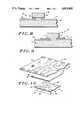
- FIG. 1shows a conventional TAB arrangement wherein a semiconductor die is carried by a tape
- FIG. 2is a view taken along lines 2--2 in FIG. 1;
- FIG. 3illustrates how the die of FIG. 1 is mounted on a substrate carrier after having been removed from its tape carrier
- FIG. 4is a perspective view of a die mounted on a tape carrier in accordance with one aspect of the invention.
- FIG. 5is a view taken along lines 5--5 in FIG. 4;
- FIG. 6is an expanded view of some of the elements between the die 37 and the tape 36 of FIG. 5;
- FIG. 7illustrates how the die of FIG. 4 is preferably mounted on a substrate carrier after having been removed from its tape carrier
- FIG. 8shows a conventional flip-chip arrangement for mounting a die on a substrate
- FIG. 9shows a flip-chip arrangement whereby a die is mounted on a substrate in accordance with the invention.
- FIG. 10shows a conductive lead pattern for use with a semiconductor die structure according to another aspect of the invention.
- FIGS. 1 and 2a conventional TAB structure 10 is shown wherein a carrier tape 12 (made of Kapton, for example) is used to hold a semiconductor die 14. This arrangement is normally used to test and otherwise handle the die 14 (and other dies that are similarly held on the non-illustrated portion of the tape 12) prior to the die being permanently mounted on a substrate.
- a carrier tape 12made of Kapton, for example
- sprocket holes 16are formed along the edges of the tape 12 to permit engagement with a rotatable sprocket (not shown) which can advance the tape and dies from one work station to another.
- Conductive test pads 18are formed on the surface of the tape 12 and are electrically connected to conductive "bumps" 20 on the die by means of conductive leads 22.
- the "bumps" 20are gold-plated metal bonding pads, each of which overlies an aluminum pad (not shown) on the die 14.
- each of the test pads 18 on the tapeis electrically connected to a corresponding pad on the die. This allows the die to be tested, prior to its separation from the tape, by exercising the functions of the die via test probes (not shown) which can be brought into contact with the test pads 18.
- the die 14is situated in a hole 24 in the tape, and that the hole is surrounded by a support ring 26 formed between the hole 24 and four cutouts 28 in the tape.
- the purpose of the ring 26is to provide support for the leads 22.
- the illustrated portion of the tape 12, along with the test pads 18 and leads 22,essentially comprise a single "site.”
- the die 14When the die 14 is ready to be removed from the tape 12 and permanently mounted on another carrier such as a substrate, the die is cut away from the tape, as along lines X--X in FIG. 2. The die and the attached portions of leads 22 are then mounted on a substrate 30 (FIG. 3) whose upper surface carries electrical conductors 32. In mounting the die on the substrate 30, the leads 22 are bent as shown to contact the desired conductors 32. Typically, each such lead will be soldered to its adjoining conductor at the point of mutual contact.
- An advantage of the conventional TAB structure described aboveis that each die can be tested while still carried by its tape. This reduces the risk of mating a defective die with a substrate (and with other circuitry carried by the substrate).
- the structure 34includes a carrier tape 36 which may be made of Mylar or the like for carrying a semiconductor die 37.
- Conventional sprocket holes 38are formed, as shown, along both edges of the tape.
- metal (e.g., copper) test pads 40 and conductive leads 42are formed by conventional techniques such as sputtering or laminating a metal foil and then photo-etching. Alternately, the leads 42 and the test pads 40 may be formed from a thick film conductive polymer.
- an adhesive/conductive element 44which consists of an anisotropically electrically conductive adhesive.
- Such an adhesivepreferably includes internal conductive particles that are dispersed so as to provide electrical conductivity only in the vertical axis. In the lateral and longitudinal axes of the adhesive, minimal conductivity is exhibited.
- Z-AXIS Interconnect FilmThis film is available from the Sheldahl Company, Northfield, Minn., and has been heretofore primarily used as a termination for flexible cables
- the element 44is contoured and situated to cover at least a portion of each lead 42 and all of the tape area below the die 37. Alternately, the element 44 may be enlarged to cover even the test pads 40, although it is preferred that the test pads remain uncovered to permit direct contact with test probes.
- the die 37has electrical contacts 46 which may be of the type known as "capped pads.” Essentially, these are conventional aluminum bonding pads covered with thin films of titanium tungsten and gold. Other types of electrical contacts, even the previously-described “bumps", may be used instead of the capped pads.
- the adhesive/conductive element 44various forms of it may be used.
- itwhen used in a liquid form, it can be rolled or printed onto the tape 36.
- an appropriately-sized piece of itmay be cut out and pressed into place on the tape 36. Its adhesiveness will hold it in place on the tape and will also hold the die 37 when the die is pressed into place on the element 44.
- the die 37is more easily aligned such that each of its electrical contacts 46 is in registration with its mating lead 42.
- the adhesive/conductive element 44will be laid down as a so-called "B-stage epoxy” or similar material which remains tacky until it has been fully cured by means of heat, ultraviolet radiation, or other means.
- B-stage epoxyor similar material which remains tacky until it has been fully cured by means of heat, ultraviolet radiation, or other means.
- the illustrated structureis now in condition for the die 37 to be tested, as by the use of test probes applied to the test pads 40.
- An electrical connectionis provided between each test pad 40 and the die 37 via a path which includes a lead 42, the portion of the adhesive/conductive element 44 that lies sandwiched between the inner end of the lead 42 and its overlying electrical contact 46, and the contact 46 itself.
- the anisotropic conductivity of the adhesive/conductive element 44permits current to flow only in the direction illustrated by the arrow 48 to complete an electrical path between the illustrated lead 42 and the overlying electrical contact 46. Conduction in other directions does not occur to any substantial degree.
- the die 37may be lifted off the element 44 and replaced by a different die.
- the die site on the tape 36is reusable, thus providing a less expensive TAB process.
- the tape site structurecomprising the die 37, the adhesive element 44, the leads 32 and the underlying portion of the tape 36, will eventually be permanently mounted on a different carrier which may be a ceramic substrate, a printed circuit board, or another device intended to be a permanent or semi-permanent support for the die. That process will now be described.
- That portion of the adhesive element 44 which underlies the die 37may be cured, leaving the reminder of the element 44 in its uncured state. This may be accomplished by directing ultraviolet radiation or localized heat only to the portion of element 44 that is directly beneath the die 37. This selective curing will firmly bond the die 37 and the tape 36 to the adhesive element 44.
- the diemay be removed from the main body of the tape carrier by cutting through the tape along the perimeter of the adhesive element 44.
- the die 37carrying with it the attached adhesive element 44, the leads 42, and the portion of the tape 36 underlying the adhesive element 44, is flipped over and mounted on a different carrier such as the substrate 52 as shown in FIG. 7.
- a different carriersuch as the substrate 52 as shown in FIG. 7.
- the conductors 54may be conventional photo-etched conductive patterns whose opposite ends (not shown) connect to other circuit elements on the substrate 52.
- each conductor 54When the die 37 is properly mounted on the substrate 52, each conductor 54 is vertically aligned with a corresponding lead 42, thereby establishing a path of electrical conductivity from each conductor 54 to a corresponding electrical contact 46 on the die 37.
- the conductivity pathis as follows. From the conductor 54, the path of electrical conductivity extends vertically upward through the adhesive element 44 (which conducts only in the vertical direction) to the adjacent lead 42. Thence, the path follows the lead 42 upwardly and to the left up to the illustrated termination of the lead 42. The path continues downwardly, again through the adhesive element 44, to the electrical contact 46.
- the die 37may now be permanently bonded to the substrate by curing the previously-uncured portions of the adhesive element 44. This may be accomplished by heating the entire structure shown in FIG. 7 in an oven to ensure that all adhesive becomes fully cured.
- FIG. 7Another important advantage of the structure shown in FIG. 7 is that the die 37 is sealed from the environment both by the tape 36 that remains over the die, and by the cured adhesive that surrounds the die. Compare this to the conventional structure shown in FIG. 3 wherein the die 14 is exposed to the environment. As a result of such sealing, the structure shown in FIG. 7 is particularly well-suited for use in harsh environments, including under-the-hood automotive applications.
- the inventionmay be applied to semiconductor structures which differ from those discussed above.
- conventional flip-chip structuresmay be modified so as to use the same type of adhesive/conductive element as previously described.
- FIG. 8a conventional flip-chip structure 56 is shown wherein a semiconductor die 58 carries solder bumps 60 for making electrical contact between the die and conductors 62 on a carrier substrate 64.
- a flip-chip structure 66 that is modified per the present inventionis shown in FIG. 9.
- a die 68carries electrical contacts in the form of capped pads 70.
- An anisotropically electrically conductive adhesive 72is situated as shown to bond the die 68 to a carrier substrate 74 and to electrical conductors 76 carried on the upper surface of the substrate.
- the element 72conducts substantially only in the vertical direction so as to provide a conductive path from each electrical contact 70 to its underlying conductor 76.
- the resistivity of the adhesive/conductive layermay need to be reduced.
- the surface area of the contact 46 which faces the element 44may be in the order of about 4 square mils.
- the resistivity of the element 44may be about 10 ohms, as measured between the contact 46 and the conductor 42.
- 10 ohmsmay be more resistance than is desirable. The method presented herein for lowering such resistance will now be described with reference to FIG. 10.
- the illustrated semiconductor die 78has an upper surface on which conductive patterns 80, 82, 84, 85 and 86 have been formed for input/output pads. Clearly, the surface areas of the illustrated patterns 80, 82, and 84 are relatively enlarged in comparison to the surface areas of the conventionally sized pads 85 and 86.
- the die 78will be covered by an adhesive/conductive layer 87 of the type described previously.
- a tape carrier 88is situated immediately above the layer 87 and carries a pattern of relatively enlarged conductive pads 90, 92, 94 whose geometry corresponds with the geometry of patterns 80, 82 and 84 on the die 78.
- a pattern of smaller, conventional pads such as 96 and 98 on the tape 88also corresponds to the geometry of the smaller pads such as 85 and 86 on the die 78.
- This arrangementprovides enlarged surface areas, as needed, for the conductive patterns of selected input/output pads.
- the resistivity of the layer 86 between themhas also been reduced. No such enlargement is required for the patterns whose input/output pads can tolerate a higher resistance through the layer 86.
- enlarged conductorsare applicable to the structures shown in FIGS. 4, 7 and 9.
- a pattern of enlarged conductorscould be used on the die 37 and the tape 36 of FIGS. 4 and 7.
- a pattern of enlarged conductorscould be used on the die 68 and the substrate 74 of FIG. 9.
Landscapes
- Engineering & Computer Science (AREA)
- Computer Hardware Design (AREA)
- Microelectronics & Electronic Packaging (AREA)
- Power Engineering (AREA)
- Physics & Mathematics (AREA)
- Condensed Matter Physics & Semiconductors (AREA)
- General Physics & Mathematics (AREA)
- Manufacturing & Machinery (AREA)
- Chemical & Material Sciences (AREA)
- Materials Engineering (AREA)
- Wire Bonding (AREA)
Abstract
Description
Claims (12)
Priority Applications (1)
| Application Number | Priority Date | Filing Date | Title |
|---|---|---|---|
| US07/029,294US4811081A (en) | 1987-03-23 | 1987-03-23 | Semiconductor die bonding with conductive adhesive |
Applications Claiming Priority (1)
| Application Number | Priority Date | Filing Date | Title |
|---|---|---|---|
| US07/029,294US4811081A (en) | 1987-03-23 | 1987-03-23 | Semiconductor die bonding with conductive adhesive |
Publications (1)
| Publication Number | Publication Date |
|---|---|
| US4811081Atrue US4811081A (en) | 1989-03-07 |
Family
ID=21848280
Family Applications (1)
| Application Number | Title | Priority Date | Filing Date |
|---|---|---|---|
| US07/029,294Expired - LifetimeUS4811081A (en) | 1987-03-23 | 1987-03-23 | Semiconductor die bonding with conductive adhesive |
Country Status (1)
| Country | Link |
|---|---|
| US (1) | US4811081A (en) |
Cited By (100)
| Publication number | Priority date | Publication date | Assignee | Title |
|---|---|---|---|---|
| US4859268A (en)* | 1986-02-24 | 1989-08-22 | International Business Machines Corporation | Method of using electrically conductive composition |
| US4949148A (en)* | 1989-01-11 | 1990-08-14 | Bartelink Dirk J | Self-aligning integrated circuit assembly |
| EP0449496A1 (en)* | 1990-03-20 | 1991-10-02 | Sharp Kabushiki Kaisha | Method for mounting a semiconductor device |
| EP0435093A3 (en)* | 1989-12-27 | 1991-11-06 | Motorola, Inc. | Thin, molded, surface mount electronic device |
| US5115299A (en)* | 1989-07-13 | 1992-05-19 | Gte Products Corporation | Hermetically sealed chip carrier with ultra violet transparent cover |
| US5147210A (en)* | 1988-03-03 | 1992-09-15 | Western Digital Corporation | Polymer film interconnect |
| WO1993010573A1 (en)* | 1991-11-22 | 1993-05-27 | Clements James R | Die mounting with uniaxial conductive adhesive |
| US5220488A (en)* | 1985-09-04 | 1993-06-15 | Ufe Incorporated | Injection molded printed circuits |
| US5220724A (en)* | 1990-09-08 | 1993-06-22 | Robert Bosch Gmbh | Method of securing surface-mounted devices to a substrate |
| EP0553557A1 (en)* | 1992-01-15 | 1993-08-04 | Advanced Micro Devices, Inc. | Process for making a multilayer lead frame assembly for an integrated circuit structure and multilayer integrated circuit die package formed by such process |
| US5261156A (en)* | 1991-02-28 | 1993-11-16 | Semiconductor Energy Laboratory Co., Ltd. | Method of electrically connecting an integrated circuit to an electric device |
| US5290710A (en)* | 1990-11-28 | 1994-03-01 | International Business Machines Corporation | Method for testing integrated circuits on a carrier substrate |
| US5294827A (en)* | 1992-12-14 | 1994-03-15 | Motorola, Inc. | Semiconductor device having thin package body and method for making the same |
| WO1994018707A1 (en)* | 1993-02-04 | 1994-08-18 | Motorola, Inc. | Thermally conductive integrated circuit package with radio frequency shielding |
| US5355102A (en)* | 1990-04-05 | 1994-10-11 | General Electric Company | HDI impedance matched microwave circuit assembly |
| US5425647A (en)* | 1992-04-29 | 1995-06-20 | Alliedsignal Inc. | Split conductive pad for mounting components to a circuit board |
| US5448106A (en)* | 1991-08-20 | 1995-09-05 | Kabushiki Kaisha Toshiba | Thin semiconductor integrated circuit device assembly |
| US5461255A (en)* | 1992-09-18 | 1995-10-24 | Texas Instruments Incorporated | Multi-layered lead frame assembly for integrated circuits |
| US5517752A (en)* | 1992-05-13 | 1996-05-21 | Fujitsu Limited | Method of connecting a pressure-connector terminal of a device with a terminal electrode of a substrate |
| US5531942A (en)* | 1994-06-16 | 1996-07-02 | Fry's Metals, Inc. | Method of making electroconductive adhesive particles for Z-axis application |
| US5542602A (en)* | 1994-12-30 | 1996-08-06 | International Business Machines Corporation | Stabilization of conductive adhesive by metallurgical bonding |
| US5543585A (en)* | 1994-02-02 | 1996-08-06 | International Business Machines Corporation | Direct chip attachment (DCA) with electrically conductive adhesives |
| US5559369A (en)* | 1989-10-02 | 1996-09-24 | Advanced Micro Devices, Inc. | Ground plane for plastic encapsulated integrated circuit die packages |
| US5559372A (en)* | 1994-12-19 | 1996-09-24 | Goldstar Electron Co., Ltd. | Thin soldered semiconductor package |
| US5585666A (en)* | 1990-04-24 | 1996-12-17 | Seiko Epson Corporation | Semiconductor device with chip layout having inner electrode configuration and liquid crystal display apparatus employing the semiconductor device |
| US5604379A (en)* | 1994-09-21 | 1997-02-18 | Sharp Kabushiki Kaisha | Semiconductor device having external electrodes formed in concave portions of an anisotropic conductive film |
| US5611884A (en)* | 1995-12-11 | 1997-03-18 | Dow Corning Corporation | Flip chip silicone pressure sensitive conductive adhesive |
| US5627730A (en)* | 1994-11-30 | 1997-05-06 | Ncr Corporation | Printed circuit board assembly for high speed data transfer |
| US5631191A (en)* | 1993-08-27 | 1997-05-20 | Poly-Flex Circuits, Inc. | Method for connecting a die to electrically conductive traces on a flexible lead-frame |
| US5637176A (en)* | 1994-06-16 | 1997-06-10 | Fry's Metals, Inc. | Methods for producing ordered Z-axis adhesive materials, materials so produced, and devices, incorporating such materials |
| US5677576A (en)* | 1995-03-24 | 1997-10-14 | Shinko Electric Industries Co., Ltd. | Chip sized semiconductor device |
| US5734201A (en)* | 1993-11-09 | 1998-03-31 | Motorola, Inc. | Low profile semiconductor device with like-sized chip and mounting substrate |
| US5822191A (en)* | 1994-08-04 | 1998-10-13 | Sharp Kabushiki Kaisha | Integrated circuit mounting tape |
| US5846853A (en)* | 1991-12-11 | 1998-12-08 | Mitsubishi Denki Kabushiki Kaisha | Process for bonding circuit substrates using conductive particles and back side exposure |
| US5861661A (en)* | 1995-12-27 | 1999-01-19 | Industrial Technology Research Institute | Composite bump tape automated bonded structure |
| US5886415A (en)* | 1996-01-19 | 1999-03-23 | Shinko Electric Industries, Co., Ltd. | Anisotropic conductive sheet and printed circuit board |
| EP0758146A3 (en)* | 1995-08-07 | 1999-08-04 | Mitsubishi Denki Kabushiki Kaisha | Flip chip semiconductor device |
| US5951323A (en)* | 1997-09-05 | 1999-09-14 | California Institute Of Technology | Connector for semiconductor microelectrodes and flexible wiring |
| US5980682A (en)* | 1998-05-14 | 1999-11-09 | Lexmark International, Inc. | Thermal printhead manufacture |
| US5986335A (en)* | 1995-12-01 | 1999-11-16 | Texas Instruments Incorporated | Semiconductor device having a tapeless mounting |
| US5990563A (en)* | 1995-12-29 | 1999-11-23 | Lg Semicon Co., Ltd. | Semiconductor package having a connection member |
| US6000603A (en)* | 1997-05-23 | 1999-12-14 | 3M Innovative Properties Company | Patterned array of metal balls and methods of making |
| US6011315A (en)* | 1996-12-13 | 2000-01-04 | Sharp Kabushiki Kaisha | Semiconductor device and film carrier tape and respective manufacturing methods thereof |
| EP0896368A4 (en)* | 1997-01-23 | 2000-03-01 | Seiko Epson Corp | FILM SUPPORT STRIP, SEMICONDUCTOR ASSEMBLY AND DEVICE, MANUFACTURING METHOD THEREOF, MOUNTING PLATE AND ELECTRONIC EQUIPMENT |
| US6060782A (en)* | 1998-01-26 | 2000-05-09 | Sharp Kabushiki Kaisha | Semiconductor device with improved mounting on tape-shaped insulating substrate |
| US6111308A (en)* | 1991-06-05 | 2000-08-29 | Advanced Micro Devices, Inc. | Ground plane for plastic encapsulated integrated circuit die packages |
| US6139661A (en)* | 1998-10-20 | 2000-10-31 | International Business Machines Corporation | Two step SMT method using masked cure |
| US6198170B1 (en)* | 1999-12-16 | 2001-03-06 | Conexant Systems, Inc. | Bonding pad and support structure and method for their fabrication |
| US6268739B1 (en) | 1998-03-30 | 2001-07-31 | International Business Machines Corporation | Method and device for semiconductor testing using electrically conductive adhesives |
| US6284086B1 (en)* | 1999-08-05 | 2001-09-04 | Three - Five Systems, Inc. | Apparatus and method for attaching a microelectronic device to a carrier using a photo initiated anisotropic conductive adhesive |
| US20010031514A1 (en)* | 1993-12-17 | 2001-10-18 | Smith John Stephen | Method and apparatus for fabricating self-assembling microstructures |
| EP1170794A1 (en)* | 2000-07-07 | 2002-01-09 | Alstom | Method of fabricating a power electronic component and power electronic component obtained thereby |
| US6340840B1 (en)* | 1999-12-14 | 2002-01-22 | Sony Corporation | Lead frame and production method thereof, and semiconductor device and fabrication method thereof |
| US6372526B1 (en)* | 1998-04-06 | 2002-04-16 | Semiconductor Components Industries Llc | Method of manufacturing semiconductor components |
| US6392306B1 (en)* | 1990-09-24 | 2002-05-21 | Tessera, Inc. | Semiconductor chip assembly with anisotropic conductive adhesive connections |
| US6409866B1 (en)* | 1999-05-28 | 2002-06-25 | Sony Chemicals Corp. | Process for mounting semiconductor device |
| US6461890B1 (en) | 1996-12-27 | 2002-10-08 | Rohm Co., Ltd. | Structure of semiconductor chip suitable for chip-on-board system and methods of fabricating and mounting the same |
| US6489183B1 (en) | 1998-07-17 | 2002-12-03 | Micron Technology, Inc. | Method of manufacturing a taped semiconductor device |
| US20020179330A1 (en)* | 1998-01-26 | 2002-12-05 | Tessera, Inc. | Compliant semiconductor package with anisotropic conductive material interconnects and methods therefor |
| US6528867B1 (en)* | 1997-08-05 | 2003-03-04 | Micron Technology, Inc. | Integrated circuit devices including connection components mechanically and electrically attached to semiconductor dice |
| US20030056976A1 (en)* | 1998-09-22 | 2003-03-27 | Kabushiki Kaisha Toshiba | Fabricating method of semiconductor devices, fabricating method of printed wired boards, and printed wired board |
| US20030062518A1 (en)* | 1999-12-17 | 2003-04-03 | Mark Auch | Method for encapsulation of electronic devices |
| US6548896B2 (en)* | 2000-04-04 | 2003-04-15 | General Electric Company | Method of reducing shear stresses on IC chips and structure formed thereby |
| US20030094691A1 (en)* | 1999-12-17 | 2003-05-22 | Mark Auch | Encapsulation of electronic devices |
| US6590285B1 (en)* | 1998-04-28 | 2003-07-08 | International Business Machines Corporation | Method and composition for mounting an electronic component and device formed therewith |
| US20030132776A1 (en)* | 1998-10-05 | 2003-07-17 | Cobbley Chad A. | Method for in-line testing of flip-chip semiconductor assemblies |
| US6605951B1 (en)* | 2000-12-11 | 2003-08-12 | Lsi Logic Corporation | Interconnector and method of connecting probes to a die for functional analysis |
| US6640415B2 (en) | 1999-06-07 | 2003-11-04 | Formfactor, Inc. | Segmented contactor |
| US20030216068A1 (en)* | 2002-05-15 | 2003-11-20 | Weiss Roger E. | Optically transparent elastomeric interconnects and method of using same |
| US6690185B1 (en)* | 1997-01-15 | 2004-02-10 | Formfactor, Inc. | Large contactor with multiple, aligned contactor units |
| US20040026795A1 (en)* | 2000-05-19 | 2004-02-12 | International Rectifier Corporation | Five layer adhesive/insulator/metal/insulator/adhesive tape for semiconductor die packaging |
| EP1213751A3 (en)* | 2000-11-30 | 2004-04-21 | Philips Intellectual Property & Standards GmbH | Semiconductor module with an interconnection structure |
| US20040085083A1 (en)* | 2002-11-06 | 2004-05-06 | Kevan Tan | Die location on ungrounded wafer for back-side emission microscopy |
| US6741085B1 (en) | 1993-11-16 | 2004-05-25 | Formfactor, Inc. | Contact carriers (tiles) for populating larger substrates with spring contacts |
| US6759732B1 (en) | 1990-04-24 | 2004-07-06 | Seiko Epson Corporation | Semiconductor device with circuit cell array and arrangement on a semiconductor chip |
| EP1448034A1 (en)* | 1996-12-27 | 2004-08-18 | Matsushita Electric Industrial Co., Ltd. | Method and device for mounting electronic component on circuit board |
| US20040212389A1 (en)* | 2003-04-23 | 2004-10-28 | Hamren Steven L. | Method and apparatus for processing semiconductor devices in a singulated form |
| US6825552B2 (en) | 2001-05-09 | 2004-11-30 | Tessera, Inc. | Connection components with anisotropic conductive material interconnection |
| US20040256739A1 (en)* | 1998-07-01 | 2004-12-23 | Seiko Epson Corporation | Semiconductor device and method of manufacture thereof, circuit board and electronic instrument |
| US20050010395A1 (en)* | 2003-07-08 | 2005-01-13 | Industrial Technology Research Institute | Scale factor based bit shifting in fine granularity scalability audio coding |
| US6911729B1 (en)* | 1999-05-14 | 2005-06-28 | Sharp Kabushiki Kaisha | Tape carrier semiconductor device |
| WO2005013358A3 (en)* | 2003-07-31 | 2005-07-21 | Siemens Ag | Arrangement of an electrical component placed on a substrate, and method for producing the same |
| US20050155706A1 (en)* | 1999-01-29 | 2005-07-21 | Kazuto Nishida | Electronic component mounting method and apparatus |
| US6938783B2 (en)* | 2000-07-26 | 2005-09-06 | Amerasia International Technology, Inc. | Carrier tape |
| US20050230843A1 (en)* | 2000-02-24 | 2005-10-20 | Williams Vernon M | Flip-chip type semiconductor devices and conductive elements thereof |
| US20060210237A1 (en)* | 2005-03-18 | 2006-09-21 | Kaoru Soeta | Electronic function part mounted body and method of manufacturing the electronic function part mounted body |
| US20070034997A1 (en)* | 2005-08-04 | 2007-02-15 | Michael Bauer | Semiconductor device with conductor tracks between semiconductor chip and circuit carrier and method for producing the same |
| US20070045882A1 (en)* | 2005-08-31 | 2007-03-01 | Ho Soo K | Double mold optocoupler |
| US20070145566A1 (en)* | 2001-10-02 | 2007-06-28 | Cardiac Pacemakers, Inc., | Method and system of tape automated bonding |
| US20070261233A1 (en)* | 1994-04-26 | 2007-11-15 | Fujitsu Limited | Method and system for fabricating a semiconductor device |
| US20080122051A1 (en)* | 2006-11-29 | 2008-05-29 | Horst Theuss | Module comprising polymer-containing electrical connecting element |
| US20090136712A1 (en)* | 2007-11-28 | 2009-05-28 | Seiko Epson Corporation | Film-like adhesive and method for carrying the same |
| US20090154106A1 (en)* | 2007-12-17 | 2009-06-18 | Lynch Thomas W | Double bonded heat dissipation |
| WO2011063082A3 (en)* | 2009-11-20 | 2011-11-24 | 3M Innovative Properties Company | Surface-modified adhesives |
| US20110309529A1 (en)* | 2010-06-16 | 2011-12-22 | Hynix Semiconductor Inc. | Module substrate that allows replacement of faulty chips, semiconductor module having the same, and method for manufacturing the semiconductor module |
| US8097963B1 (en)* | 2009-04-28 | 2012-01-17 | Maxim Integrated Products, Inc. | Electrically conductive matrix for z-axis interconnect |
| US20130286644A1 (en)* | 2012-04-25 | 2013-10-31 | Hon Hai Precision Industry Co., Ltd. | Led light bar with balanced resistance for light emtitting diodes thereof |
| CN103904189A (en)* | 2012-12-25 | 2014-07-02 | 鸿富锦精密工业(深圳)有限公司 | Luminescence chip combination and manufacturing method thereof |
| US20180019196A1 (en)* | 2016-07-12 | 2018-01-18 | Shinko Electric Industries Co., Ltd. | Wiring substrate and semiconductor package |
| US20230230966A1 (en)* | 2022-01-14 | 2023-07-20 | Advanced Semiconductor Engineering, Inc. | Electronic package and electronic device |
Citations (4)
| Publication number | Priority date | Publication date | Assignee | Title |
|---|---|---|---|---|
| US3818279A (en)* | 1973-02-08 | 1974-06-18 | Chromerics Inc | Electrical interconnection and contacting system |
| US4147889A (en)* | 1978-02-28 | 1979-04-03 | Amp Incorporated | Chip carrier |
| US4577214A (en)* | 1981-05-06 | 1986-03-18 | At&T Bell Laboratories | Low-inductance power/ground distribution in a package for a semiconductor chip |
| US4631820A (en)* | 1984-08-23 | 1986-12-30 | Canon Kabushiki Kaisha | Mounting assembly and mounting method for an electronic component |
- 1987
- 1987-03-23USUS07/029,294patent/US4811081A/ennot_activeExpired - Lifetime
Patent Citations (4)
| Publication number | Priority date | Publication date | Assignee | Title |
|---|---|---|---|---|
| US3818279A (en)* | 1973-02-08 | 1974-06-18 | Chromerics Inc | Electrical interconnection and contacting system |
| US4147889A (en)* | 1978-02-28 | 1979-04-03 | Amp Incorporated | Chip carrier |
| US4577214A (en)* | 1981-05-06 | 1986-03-18 | At&T Bell Laboratories | Low-inductance power/ground distribution in a package for a semiconductor chip |
| US4631820A (en)* | 1984-08-23 | 1986-12-30 | Canon Kabushiki Kaisha | Mounting assembly and mounting method for an electronic component |
Cited By (198)
| Publication number | Priority date | Publication date | Assignee | Title |
|---|---|---|---|---|
| US5220488A (en)* | 1985-09-04 | 1993-06-15 | Ufe Incorporated | Injection molded printed circuits |
| US4859268A (en)* | 1986-02-24 | 1989-08-22 | International Business Machines Corporation | Method of using electrically conductive composition |
| US5147210A (en)* | 1988-03-03 | 1992-09-15 | Western Digital Corporation | Polymer film interconnect |
| US4949148A (en)* | 1989-01-11 | 1990-08-14 | Bartelink Dirk J | Self-aligning integrated circuit assembly |
| US5115299A (en)* | 1989-07-13 | 1992-05-19 | Gte Products Corporation | Hermetically sealed chip carrier with ultra violet transparent cover |
| US5559369A (en)* | 1989-10-02 | 1996-09-24 | Advanced Micro Devices, Inc. | Ground plane for plastic encapsulated integrated circuit die packages |
| EP0435093A3 (en)* | 1989-12-27 | 1991-11-06 | Motorola, Inc. | Thin, molded, surface mount electronic device |
| EP0449496A1 (en)* | 1990-03-20 | 1991-10-02 | Sharp Kabushiki Kaisha | Method for mounting a semiconductor device |
| US5355102A (en)* | 1990-04-05 | 1994-10-11 | General Electric Company | HDI impedance matched microwave circuit assembly |
| US5585666A (en)* | 1990-04-24 | 1996-12-17 | Seiko Epson Corporation | Semiconductor device with chip layout having inner electrode configuration and liquid crystal display apparatus employing the semiconductor device |
| US6759732B1 (en) | 1990-04-24 | 2004-07-06 | Seiko Epson Corporation | Semiconductor device with circuit cell array and arrangement on a semiconductor chip |
| US6204567B1 (en)* | 1990-04-24 | 2001-03-20 | Seiko Epson Corporation | Semiconductor device with circuit cell array and arrangement on a semiconductor chip |
| US5220724A (en)* | 1990-09-08 | 1993-06-22 | Robert Bosch Gmbh | Method of securing surface-mounted devices to a substrate |
| US6392306B1 (en)* | 1990-09-24 | 2002-05-21 | Tessera, Inc. | Semiconductor chip assembly with anisotropic conductive adhesive connections |
| US5290710A (en)* | 1990-11-28 | 1994-03-01 | International Business Machines Corporation | Method for testing integrated circuits on a carrier substrate |
| US5261156A (en)* | 1991-02-28 | 1993-11-16 | Semiconductor Energy Laboratory Co., Ltd. | Method of electrically connecting an integrated circuit to an electric device |
| US6111308A (en)* | 1991-06-05 | 2000-08-29 | Advanced Micro Devices, Inc. | Ground plane for plastic encapsulated integrated circuit die packages |
| US5448106A (en)* | 1991-08-20 | 1995-09-05 | Kabushiki Kaisha Toshiba | Thin semiconductor integrated circuit device assembly |
| US5258577A (en)* | 1991-11-22 | 1993-11-02 | Clements James R | Die mounting with uniaxial conductive adhesive |
| WO1993010573A1 (en)* | 1991-11-22 | 1993-05-27 | Clements James R | Die mounting with uniaxial conductive adhesive |
| US5846853A (en)* | 1991-12-11 | 1998-12-08 | Mitsubishi Denki Kabushiki Kaisha | Process for bonding circuit substrates using conductive particles and back side exposure |
| EP0553557A1 (en)* | 1992-01-15 | 1993-08-04 | Advanced Micro Devices, Inc. | Process for making a multilayer lead frame assembly for an integrated circuit structure and multilayer integrated circuit die package formed by such process |
| US5425647A (en)* | 1992-04-29 | 1995-06-20 | Alliedsignal Inc. | Split conductive pad for mounting components to a circuit board |
| US5517752A (en)* | 1992-05-13 | 1996-05-21 | Fujitsu Limited | Method of connecting a pressure-connector terminal of a device with a terminal electrode of a substrate |
| US5461255A (en)* | 1992-09-18 | 1995-10-24 | Texas Instruments Incorporated | Multi-layered lead frame assembly for integrated circuits |
| US5294827A (en)* | 1992-12-14 | 1994-03-15 | Motorola, Inc. | Semiconductor device having thin package body and method for making the same |
| WO1994018707A1 (en)* | 1993-02-04 | 1994-08-18 | Motorola, Inc. | Thermally conductive integrated circuit package with radio frequency shielding |
| US5371404A (en)* | 1993-02-04 | 1994-12-06 | Motorola, Inc. | Thermally conductive integrated circuit package with radio frequency shielding |
| US5631191A (en)* | 1993-08-27 | 1997-05-20 | Poly-Flex Circuits, Inc. | Method for connecting a die to electrically conductive traces on a flexible lead-frame |
| US5734201A (en)* | 1993-11-09 | 1998-03-31 | Motorola, Inc. | Low profile semiconductor device with like-sized chip and mounting substrate |
| US6741085B1 (en) | 1993-11-16 | 2004-05-25 | Formfactor, Inc. | Contact carriers (tiles) for populating larger substrates with spring contacts |
| US20040163252A1 (en)* | 1993-11-16 | 2004-08-26 | Formfactor, Inc. | Contact carriers (tiles) for populating larger substrates with spring contacts |
| US7714598B2 (en) | 1993-11-16 | 2010-05-11 | Formfactor, Inc. | Contact carriers (tiles) for populating larger substrates with spring contacts |
| US7347702B2 (en) | 1993-11-16 | 2008-03-25 | Formfactor, Inc. | Contact carriers (tiles) for populating larger substrates with spring contacts |
| US20070075715A1 (en)* | 1993-11-16 | 2007-04-05 | Formfactor, Inc. | Contact Carriers (Tiles) For Populating Larger Substrates With Spring Contacts |
| US7140883B2 (en) | 1993-11-16 | 2006-11-28 | Formfactor, Inc. | Contact carriers (tiles) for populating larger substrates with spring contacts |
| US20080231305A1 (en)* | 1993-11-16 | 2008-09-25 | Formfactor, Inc. | Contact carriers (tiles) for populating larger substrates with spring contacts |
| US20100075463A1 (en)* | 1993-12-17 | 2010-03-25 | The Regents Of The University Of California | Method and apparatus for fabricating self-assembling microstructures |
| US20010031514A1 (en)* | 1993-12-17 | 2001-10-18 | Smith John Stephen | Method and apparatus for fabricating self-assembling microstructures |
| US7727804B2 (en) | 1993-12-17 | 2010-06-01 | The Regents Of The University Of California | Method and apparatus for fabricating self-assembling microstructures |
| US6864570B2 (en) | 1993-12-17 | 2005-03-08 | The Regents Of The University Of California | Method and apparatus for fabricating self-assembling microstructures |
| US5543585A (en)* | 1994-02-02 | 1996-08-06 | International Business Machines Corporation | Direct chip attachment (DCA) with electrically conductive adhesives |
| US20070281395A1 (en)* | 1994-04-26 | 2007-12-06 | Fujitsu Limited | Method and system for fabricating a semiconductor device |
| US20070261233A1 (en)* | 1994-04-26 | 2007-11-15 | Fujitsu Limited | Method and system for fabricating a semiconductor device |
| US5637176A (en)* | 1994-06-16 | 1997-06-10 | Fry's Metals, Inc. | Methods for producing ordered Z-axis adhesive materials, materials so produced, and devices, incorporating such materials |
| US5531942A (en)* | 1994-06-16 | 1996-07-02 | Fry's Metals, Inc. | Method of making electroconductive adhesive particles for Z-axis application |
| US5822191A (en)* | 1994-08-04 | 1998-10-13 | Sharp Kabushiki Kaisha | Integrated circuit mounting tape |
| US5604379A (en)* | 1994-09-21 | 1997-02-18 | Sharp Kabushiki Kaisha | Semiconductor device having external electrodes formed in concave portions of an anisotropic conductive film |
| US5627730A (en)* | 1994-11-30 | 1997-05-06 | Ncr Corporation | Printed circuit board assembly for high speed data transfer |
| US5559372A (en)* | 1994-12-19 | 1996-09-24 | Goldstar Electron Co., Ltd. | Thin soldered semiconductor package |
| US5542602A (en)* | 1994-12-30 | 1996-08-06 | International Business Machines Corporation | Stabilization of conductive adhesive by metallurgical bonding |
| US5677576A (en)* | 1995-03-24 | 1997-10-14 | Shinko Electric Industries Co., Ltd. | Chip sized semiconductor device |
| EP0758146A3 (en)* | 1995-08-07 | 1999-08-04 | Mitsubishi Denki Kabushiki Kaisha | Flip chip semiconductor device |
| US5986335A (en)* | 1995-12-01 | 1999-11-16 | Texas Instruments Incorporated | Semiconductor device having a tapeless mounting |
| EP0779653A3 (en)* | 1995-12-11 | 1999-01-20 | Dow Corning Corporation | Flip chip silicone pressure sensitive conductive adhesive |
| US5611884A (en)* | 1995-12-11 | 1997-03-18 | Dow Corning Corporation | Flip chip silicone pressure sensitive conductive adhesive |
| US5861661A (en)* | 1995-12-27 | 1999-01-19 | Industrial Technology Research Institute | Composite bump tape automated bonded structure |
| US5990563A (en)* | 1995-12-29 | 1999-11-23 | Lg Semicon Co., Ltd. | Semiconductor package having a connection member |
| US6121688A (en)* | 1996-01-19 | 2000-09-19 | Shinko Electric Industries Co., Ltd. | Anisotropic conductive sheet and printed circuit board |
| US5886415A (en)* | 1996-01-19 | 1999-03-23 | Shinko Electric Industries, Co., Ltd. | Anisotropic conductive sheet and printed circuit board |
| US6011315A (en)* | 1996-12-13 | 2000-01-04 | Sharp Kabushiki Kaisha | Semiconductor device and film carrier tape and respective manufacturing methods thereof |
| US6461890B1 (en) | 1996-12-27 | 2002-10-08 | Rohm Co., Ltd. | Structure of semiconductor chip suitable for chip-on-board system and methods of fabricating and mounting the same |
| EP1448034A1 (en)* | 1996-12-27 | 2004-08-18 | Matsushita Electric Industrial Co., Ltd. | Method and device for mounting electronic component on circuit board |
| US6690185B1 (en)* | 1997-01-15 | 2004-02-10 | Formfactor, Inc. | Large contactor with multiple, aligned contactor units |
| US6646338B2 (en) | 1997-01-23 | 2003-11-11 | Seiko Epson Corporation | Film carrier tape, semiconductor assembly, semiconductor device, and method of manufacturing the same, mounted board, and electronic instrument |
| US6414382B1 (en) | 1997-01-23 | 2002-07-02 | Seiko Epson Corporation | Film carrier tape, semiconductor assembly, semiconductor device and method of manufacturing the same, mounted board, and electronic instrument |
| EP0896368A4 (en)* | 1997-01-23 | 2000-03-01 | Seiko Epson Corp | FILM SUPPORT STRIP, SEMICONDUCTOR ASSEMBLY AND DEVICE, MANUFACTURING METHOD THEREOF, MOUNTING PLATE AND ELECTRONIC EQUIPMENT |
| US6175151B1 (en) | 1997-01-23 | 2001-01-16 | Seiko Epson Corporation | Film carrier tape, semiconductor assembly, semiconductor device, and method of manufacturing the same, mounted board, and electronic instrument |
| US6000603A (en)* | 1997-05-23 | 1999-12-14 | 3M Innovative Properties Company | Patterned array of metal balls and methods of making |
| US6528867B1 (en)* | 1997-08-05 | 2003-03-04 | Micron Technology, Inc. | Integrated circuit devices including connection components mechanically and electrically attached to semiconductor dice |
| US5951323A (en)* | 1997-09-05 | 1999-09-14 | California Institute Of Technology | Connector for semiconductor microelectrodes and flexible wiring |
| US20020179330A1 (en)* | 1998-01-26 | 2002-12-05 | Tessera, Inc. | Compliant semiconductor package with anisotropic conductive material interconnects and methods therefor |
| US6060782A (en)* | 1998-01-26 | 2000-05-09 | Sharp Kabushiki Kaisha | Semiconductor device with improved mounting on tape-shaped insulating substrate |
| US6791169B2 (en) | 1998-01-26 | 2004-09-14 | Tessera, Inc. | Compliant semiconductor package with anisotropic conductive material interconnects and methods therefor |
| US6288559B1 (en) | 1998-03-30 | 2001-09-11 | International Business Machines Corporation | Semiconductor testing using electrically conductive adhesives |
| US6559666B2 (en) | 1998-03-30 | 2003-05-06 | International Business Machines Corporation | Method and device for semiconductor testing using electrically conductive adhesives |
| US6268739B1 (en) | 1998-03-30 | 2001-07-31 | International Business Machines Corporation | Method and device for semiconductor testing using electrically conductive adhesives |
| US6372526B1 (en)* | 1998-04-06 | 2002-04-16 | Semiconductor Components Industries Llc | Method of manufacturing semiconductor components |
| US6590285B1 (en)* | 1998-04-28 | 2003-07-08 | International Business Machines Corporation | Method and composition for mounting an electronic component and device formed therewith |
| US6589376B1 (en)* | 1998-04-28 | 2003-07-08 | International Business Machines Corporation | Method and composition for mounting an electronic component and device formed therewith |
| US5980682A (en)* | 1998-05-14 | 1999-11-09 | Lexmark International, Inc. | Thermal printhead manufacture |
| US7868466B2 (en) | 1998-07-01 | 2011-01-11 | Seiko Epson Corporation | Semiconductor device and method of manufacture thereof, circuit board and electronic instrument |
| US20040256739A1 (en)* | 1998-07-01 | 2004-12-23 | Seiko Epson Corporation | Semiconductor device and method of manufacture thereof, circuit board and electronic instrument |
| US20060172460A1 (en)* | 1998-07-01 | 2006-08-03 | Seiko Epson Corporation | Semiconductor device and method of manufacture thereof, circuit board and electronic instrument |
| US7332371B2 (en) | 1998-07-01 | 2008-02-19 | Seiko Epson Corporation | Semiconductor device and method of manufacture thereof, circuit board and electronic instrument |
| US20080128921A1 (en)* | 1998-07-01 | 2008-06-05 | Seiko Epson Corporation | Semiconductor device and method of manufacture thereof, circuit board and electronic instrument |
| US20060267196A1 (en)* | 1998-07-17 | 2006-11-30 | Farnworth Warren M | Taped semiconductor device and method of manufacture |
| US7829385B2 (en) | 1998-07-17 | 2010-11-09 | Micron Technology, Inc. | Taped semiconductor device and method of manufacture |
| US6489183B1 (en) | 1998-07-17 | 2002-12-03 | Micron Technology, Inc. | Method of manufacturing a taped semiconductor device |
| US20030056976A1 (en)* | 1998-09-22 | 2003-03-27 | Kabushiki Kaisha Toshiba | Fabricating method of semiconductor devices, fabricating method of printed wired boards, and printed wired board |
| US6711815B2 (en)* | 1998-09-22 | 2004-03-30 | Kabushiki Kaisha Toshiba | Fabricating method of semiconductor devices |
| US6750070B2 (en) | 1998-10-05 | 2004-06-15 | Micron Technology, Inc. | Process for manufacturing flip-chip semiconductor assembly |
| US7105366B2 (en) | 1998-10-05 | 2006-09-12 | Micron Technology, Inc. | Method for in-line testing of flip-chip semiconductor assemblies |
| US20030132776A1 (en)* | 1998-10-05 | 2003-07-17 | Cobbley Chad A. | Method for in-line testing of flip-chip semiconductor assemblies |
| US20040097009A1 (en)* | 1998-10-05 | 2004-05-20 | Cobbley Chad A. | Method for packaging flip-chip semiconductor assemblies |
| US20040080332A1 (en)* | 1998-10-05 | 2004-04-29 | Cobbley Chad A | Method for manufacturing flip-chip semiconductor assembly |
| US20040104741A1 (en)* | 1998-10-05 | 2004-06-03 | Cobbley Chad A. | Method for in-line testing of flip-chip semiconductor assemblies |
| US20030141888A1 (en)* | 1998-10-05 | 2003-07-31 | Cobbley Chad A. | Method for in-line testing of flip-chip semiconductor assemblies |
| US7074648B2 (en) | 1998-10-05 | 2006-07-11 | Micron Technology, Inc. | Method for packaging flip-chip semiconductor assemblies |
| US7005878B2 (en) | 1998-10-05 | 2006-02-28 | Micron Technology, Inc. | Method for in-line testing of flip-chip semiconductor assemblies |
| US6982177B2 (en) | 1998-10-05 | 2006-01-03 | Micron Technology, Inc. | Method for in-line testing of flip-chip semiconductor assemblies |
| US6972200B2 (en) | 1998-10-05 | 2005-12-06 | Micron Technology, Inc. | Method for manufacturing flip-chip semiconductor assembly |
| US6967113B2 (en) | 1998-10-05 | 2005-11-22 | Micron Technology, Inc. | Method for in-line testing of flip-chip semiconductor assemblies |
| US6962826B2 (en) | 1998-10-05 | 2005-11-08 | Micron Technology, Inc. | Method for in-line testing of flip-chip semiconductor assemblies |
| US6953699B2 (en) | 1998-10-05 | 2005-10-11 | Micron Technology, Inc. | Method for in-line testing of flip-chip semiconductor assemblies |
| US6954081B2 (en)* | 1998-10-05 | 2005-10-11 | Micron Technology, Inc. | Method for in-line testing of flip-chip semiconductor assemblies |
| US20040263196A1 (en)* | 1998-10-05 | 2004-12-30 | Cobbley Chad A. | Method for in-line testing of flip-chip semiconductor assemblies |
| US20040263197A1 (en)* | 1998-10-05 | 2004-12-30 | Cobbley Chad A. | Method for in-line testing of flip-chip semiconductor assemblies |
| US20040263195A1 (en)* | 1998-10-05 | 2004-12-30 | Cobbley Chad A. | Method for in-line testing of flip-chip semiconductor assemblies |
| US20050007142A1 (en)* | 1998-10-05 | 2005-01-13 | Cobbley Chad A. | Method for in-line testing of flip-chip semiconductor assemblies |
| US6953700B2 (en) | 1998-10-05 | 2005-10-11 | Micron Technology, Inc. | Method for in-line testing of flip-chip semiconductor assemblies |
| US20050007141A1 (en)* | 1998-10-05 | 2005-01-13 | Cobbley Chad A. | Method for in-line testing of flip-chip semiconductor assemblies |
| US6949943B2 (en) | 1998-10-05 | 2005-09-27 | Micron Technology, Inc. | Method for in-line testing of flip-chip semiconductor assemblies |
| US20050024080A1 (en)* | 1998-10-05 | 2005-02-03 | Cobbley Chad A. | Method for in-line testing of flip-chip semiconductor assemblies |
| US6530412B1 (en) | 1998-10-20 | 2003-03-11 | International Business Machines Corporation | Surface mount technology with masked cure |
| US6139661A (en)* | 1998-10-20 | 2000-10-31 | International Business Machines Corporation | Two step SMT method using masked cure |
| US20070013067A1 (en)* | 1999-01-29 | 2007-01-18 | Kazuto Nishida | Electronic component mounting method and apparatus |
| US8007627B2 (en) | 1999-01-29 | 2011-08-30 | Panasonic Corporation | Electronic component mounting method and apparatus |
| US7683482B2 (en) | 1999-01-29 | 2010-03-23 | Panasonic Corporation | Electronic component unit |
| US20050155706A1 (en)* | 1999-01-29 | 2005-07-21 | Kazuto Nishida | Electronic component mounting method and apparatus |
| US6926796B1 (en)* | 1999-01-29 | 2005-08-09 | Matsushita Electric Industrial Co., Ltd. | Electronic parts mounting method and device therefor |
| US20050224974A1 (en)* | 1999-01-29 | 2005-10-13 | Kazuto Nishida | Electronic component mounting method and apparatus |
| US6911729B1 (en)* | 1999-05-14 | 2005-06-28 | Sharp Kabushiki Kaisha | Tape carrier semiconductor device |
| US6409866B1 (en)* | 1999-05-28 | 2002-06-25 | Sony Chemicals Corp. | Process for mounting semiconductor device |
| US20100043226A1 (en)* | 1999-06-07 | 2010-02-25 | Formfactor, Inc. | Segmented contactor |
| US20040058487A1 (en)* | 1999-06-07 | 2004-03-25 | Formfactor, Inc. | Segmented contactor |
| US7215131B1 (en) | 1999-06-07 | 2007-05-08 | Formfactor, Inc. | Segmented contactor |
| US6640415B2 (en) | 1999-06-07 | 2003-11-04 | Formfactor, Inc. | Segmented contactor |
| US8011089B2 (en) | 1999-06-07 | 2011-09-06 | Formfactor, Inc. | Method of repairing segmented contactor |
| US7578057B2 (en) | 1999-06-07 | 2009-08-25 | Formfactor, Inc. | Method of fabricating segmented contactor |
| US7065870B2 (en) | 1999-06-07 | 2006-06-27 | Formfactor, Inc. | Segmented contactor |
| US6284086B1 (en)* | 1999-08-05 | 2001-09-04 | Three - Five Systems, Inc. | Apparatus and method for attaching a microelectronic device to a carrier using a photo initiated anisotropic conductive adhesive |
| US6465279B2 (en)* | 1999-12-14 | 2002-10-15 | Sony Corporation | Lead frame and production method thereof, and semiconductor device and fabrication method thereof |
| US6340840B1 (en)* | 1999-12-14 | 2002-01-22 | Sony Corporation | Lead frame and production method thereof, and semiconductor device and fabrication method thereof |
| US6198170B1 (en)* | 1999-12-16 | 2001-03-06 | Conexant Systems, Inc. | Bonding pad and support structure and method for their fabrication |
| US7419842B2 (en) | 1999-12-17 | 2008-09-02 | Osram Gmbh | Encapsulation of electroluminescent devices with shaped spacers |
| US20030160318A1 (en)* | 1999-12-17 | 2003-08-28 | Ewald Guenther | Encapsulation of electronic devices with shaped spacers |
| US20030062518A1 (en)* | 1999-12-17 | 2003-04-03 | Mark Auch | Method for encapsulation of electronic devices |
| US7432533B2 (en) | 1999-12-17 | 2008-10-07 | Osram Gmbh | Encapsulation of electronic devices with shaped spacers |
| US20070128765A1 (en)* | 1999-12-17 | 2007-06-07 | Osram Gmbh | Encapsulation of electroluminescent devices with shaped spacers |
| US20030094691A1 (en)* | 1999-12-17 | 2003-05-22 | Mark Auch | Encapsulation of electronic devices |
| US7394153B2 (en)* | 1999-12-17 | 2008-07-01 | Osram Opto Semiconductors Gmbh | Encapsulation of electronic devices |
| US8344360B2 (en) | 1999-12-17 | 2013-01-01 | Osram Opto Semiconductor Gmbh | Organic electronic devices with an encapsulation |
| US20050230843A1 (en)* | 2000-02-24 | 2005-10-20 | Williams Vernon M | Flip-chip type semiconductor devices and conductive elements thereof |
| US6548896B2 (en)* | 2000-04-04 | 2003-04-15 | General Electric Company | Method of reducing shear stresses on IC chips and structure formed thereby |
| US20040026795A1 (en)* | 2000-05-19 | 2004-02-12 | International Rectifier Corporation | Five layer adhesive/insulator/metal/insulator/adhesive tape for semiconductor die packaging |
| US6768211B2 (en)* | 2000-05-19 | 2004-07-27 | International Rectifier Corporation | Five layer adhesive/insulator/metal/insulator/adhesive tape for semiconductor die packaging |
| US6589859B2 (en) | 2000-07-07 | 2003-07-08 | Alstom | Method of manufacturing an electronic power component, and an electronic power component obtained thereby |
| EP1170794A1 (en)* | 2000-07-07 | 2002-01-09 | Alstom | Method of fabricating a power electronic component and power electronic component obtained thereby |
| FR2811475A1 (en)* | 2000-07-07 | 2002-01-11 | Alstom | METHOD FOR MANUFACTURING AN ELECTRONIC POWER COMPONENT, AND ELECTRONIC POWER COMPONENT THUS OBTAINED |
| US6938783B2 (en)* | 2000-07-26 | 2005-09-06 | Amerasia International Technology, Inc. | Carrier tape |
| EP1213751A3 (en)* | 2000-11-30 | 2004-04-21 | Philips Intellectual Property & Standards GmbH | Semiconductor module with an interconnection structure |
| US6605951B1 (en)* | 2000-12-11 | 2003-08-12 | Lsi Logic Corporation | Interconnector and method of connecting probes to a die for functional analysis |
| US20050064626A1 (en)* | 2001-05-09 | 2005-03-24 | David Light | Connection components with anistropic conductive material interconnector |
| US6825552B2 (en) | 2001-05-09 | 2004-11-30 | Tessera, Inc. | Connection components with anisotropic conductive material interconnection |
| US20070145566A1 (en)* | 2001-10-02 | 2007-06-28 | Cardiac Pacemakers, Inc., | Method and system of tape automated bonding |
| US7713790B2 (en) | 2001-10-02 | 2010-05-11 | Cardiac Pacemakers, Inc. | Method and system of tape automated bonding |
| US20080293168A1 (en)* | 2001-10-02 | 2008-11-27 | Cardiac Pacemakers, Inc. | Method and system of tape automated bonding |
| US7405475B2 (en)* | 2001-10-02 | 2008-07-29 | Cardiac Pacemakers, Inc. | Method and system of tape automated bonding |
| US20030216068A1 (en)* | 2002-05-15 | 2003-11-20 | Weiss Roger E. | Optically transparent elastomeric interconnects and method of using same |
| US20040085083A1 (en)* | 2002-11-06 | 2004-05-06 | Kevan Tan | Die location on ungrounded wafer for back-side emission microscopy |
| US6734697B1 (en) | 2002-11-06 | 2004-05-11 | Lsi Logic Corporation | Die location on ungrounded wafer for back-side emission microscopy |
| US7126228B2 (en) | 2003-04-23 | 2006-10-24 | Micron Technology, Inc. | Apparatus for processing semiconductor devices in a singulated form |
| US7122389B2 (en) | 2003-04-23 | 2006-10-17 | Micron Technology, Inc. | Method for processing semiconductor devices in a singulated form |
| US20050017739A1 (en)* | 2003-04-23 | 2005-01-27 | Hamren Steven L. | Method and apparatus for processing semiconductor devices in a singulated form |
| US20070155029A1 (en)* | 2003-04-23 | 2007-07-05 | Hamren Steven L | Methods for processing semiconductor devices in a singulated form |
| US7456504B2 (en) | 2003-04-23 | 2008-11-25 | Micron Technology, Inc. | Electronic component assemblies with electrically conductive bonds |
| US7129721B2 (en) | 2003-04-23 | 2006-10-31 | Hamren Steven L | Method and apparatus for processing semiconductor devices in a singulated form |
| US7135345B2 (en) | 2003-04-23 | 2006-11-14 | Micron Technology, Inc. | Methods for processing semiconductor devices in a singulated form |
| US20040212389A1 (en)* | 2003-04-23 | 2004-10-28 | Hamren Steven L. | Method and apparatus for processing semiconductor devices in a singulated form |
| US20050014301A1 (en)* | 2003-04-23 | 2005-01-20 | Hamren Steven L. | Method and apparatus for processing semiconductor devices in a singulated form |
| US20050042782A1 (en)* | 2003-04-23 | 2005-02-24 | Hamren Steven L. | Method and apparatus for processing semiconductor devices in a singulated form |
| US20050010395A1 (en)* | 2003-07-08 | 2005-01-13 | Industrial Technology Research Institute | Scale factor based bit shifting in fine granularity scalability audio coding |
| WO2005013358A3 (en)* | 2003-07-31 | 2005-07-21 | Siemens Ag | Arrangement of an electrical component placed on a substrate, and method for producing the same |
| US7649272B2 (en) | 2003-07-31 | 2010-01-19 | Siemens Aktiengesellschaft | Arrangement of an electrical component placed on a substrate, and method for producing the same |
| US20060197222A1 (en)* | 2003-07-31 | 2006-09-07 | Franz Auerbach | Arrangement of an electrical component placed on a substrate, and method for producing the same |
| US20060210237A1 (en)* | 2005-03-18 | 2006-09-21 | Kaoru Soeta | Electronic function part mounted body and method of manufacturing the electronic function part mounted body |
| US7443019B2 (en)* | 2005-08-04 | 2008-10-28 | Infineon Technologies Ag | Semiconductor device with conductor tracks between semiconductor chip and circuit carrier and method for producing the same |
| US20070034997A1 (en)* | 2005-08-04 | 2007-02-15 | Michael Bauer | Semiconductor device with conductor tracks between semiconductor chip and circuit carrier and method for producing the same |
| US20070045882A1 (en)* | 2005-08-31 | 2007-03-01 | Ho Soo K | Double mold optocoupler |
| US7736070B2 (en)* | 2005-08-31 | 2010-06-15 | Avago Technologies Ecbu Ip (Singapore) Pte. Ltd. | Double mold optocoupler |
| US7745916B2 (en)* | 2006-11-29 | 2010-06-29 | Infineon Technologies Ag | Module comprising polymer-containing electrical connecting element |
| US20080122051A1 (en)* | 2006-11-29 | 2008-05-29 | Horst Theuss | Module comprising polymer-containing electrical connecting element |
| US20090136712A1 (en)* | 2007-11-28 | 2009-05-28 | Seiko Epson Corporation | Film-like adhesive and method for carrying the same |
| US20100226097A1 (en)* | 2007-12-17 | 2010-09-09 | Lynch Thomas W | Double bonded heat dissipation |
| US20090154106A1 (en)* | 2007-12-17 | 2009-06-18 | Lynch Thomas W | Double bonded heat dissipation |
| US8018722B2 (en) | 2007-12-17 | 2011-09-13 | Tanima Holdings, Llc | Double bonded heat dissipation |
| US7706144B2 (en) | 2007-12-17 | 2010-04-27 | Lynch Thomas W | Heat dissipation system and related method |
| US8097963B1 (en)* | 2009-04-28 | 2012-01-17 | Maxim Integrated Products, Inc. | Electrically conductive matrix for z-axis interconnect |
| WO2011063082A3 (en)* | 2009-11-20 | 2011-11-24 | 3M Innovative Properties Company | Surface-modified adhesives |
| US20110309529A1 (en)* | 2010-06-16 | 2011-12-22 | Hynix Semiconductor Inc. | Module substrate that allows replacement of faulty chips, semiconductor module having the same, and method for manufacturing the semiconductor module |
| US8829689B2 (en)* | 2010-06-16 | 2014-09-09 | SK Hynix Inc. | Module substrate with feature for replacement of faulty chips, semiconductor module having the same, and method for manufacturing the semiconductor module |
| US20130286644A1 (en)* | 2012-04-25 | 2013-10-31 | Hon Hai Precision Industry Co., Ltd. | Led light bar with balanced resistance for light emtitting diodes thereof |
| CN103904189A (en)* | 2012-12-25 | 2014-07-02 | 鸿富锦精密工业(深圳)有限公司 | Luminescence chip combination and manufacturing method thereof |
| US20180019196A1 (en)* | 2016-07-12 | 2018-01-18 | Shinko Electric Industries Co., Ltd. | Wiring substrate and semiconductor package |
| US10170405B2 (en)* | 2016-07-12 | 2019-01-01 | Shinko Electric Industries Co., Ltd. | Wiring substrate and semiconductor package |
| US20230230966A1 (en)* | 2022-01-14 | 2023-07-20 | Advanced Semiconductor Engineering, Inc. | Electronic package and electronic device |
| US12300681B2 (en)* | 2022-01-14 | 2025-05-13 | Advanced Semiconductor Engineering, Inc. | Electronic package and electronic device |
Similar Documents
| Publication | Publication Date | Title |
|---|---|---|
| US4811081A (en) | Semiconductor die bonding with conductive adhesive | |
| EP0856889B1 (en) | Semiconductor device mount structure and semiconductor device mounting method | |
| US5162613A (en) | Integrated circuit interconnection technique | |
| US5184207A (en) | Semiconductor die packages having lead support frame | |
| US5561323A (en) | Electronic package with thermally conductive support member having a thin circuitized substrate and semiconductor device bonded thereto | |
| US4647959A (en) | Integrated circuit package, and method of forming an integrated circuit package | |
| US5773884A (en) | Electronic package with thermally conductive support member having a thin circuitized substrate and semiconductor device bonded thereto | |
| US5633533A (en) | Electronic package with thermally conductive support member having a thin circuitized substrate and semiconductor device bonded thereto | |
| US5663530A (en) | Wire bond tape ball grid array package | |
| JPH0691180B2 (en) | Integrated circuit device | |
| US5357400A (en) | Tape automated bonding semiconductor device and production process thereof | |
| US4842373A (en) | Connecting structure for connecting a liquid crystal display and a flexible flat cable | |
| US5306664A (en) | Semiconductor device, method of forming bump electrode of a semiconductor device, method of packaging a semiconductor device, chip carrier tape, display device and electronic printing device incorporating the semiconductor device | |
| JPS6039841A (en) | Integrated circuit with conductive mount medium premounted and method of producing same | |
| KR100198682B1 (en) | Semiconductor device manufacturing method | |
| JPH11135567A (en) | Method for manufacturing anisotropic conductive film and semiconductor device | |
| JP3722325B2 (en) | Surface mount electronic component, wiring board, mounting board, and mounting method | |
| JPH09181491A (en) | Semiconductor device mounting method and mounting structure | |
| JPH03160751A (en) | semiconductor equipment | |
| JPH11330154A (en) | Flexible substrate, tape carrier package using the same, and mounting method thereof | |
| JPS63185035A (en) | Semiconductor device | |
| JP2555916B2 (en) | Film carrier semiconductor device | |
| JPH02252248A (en) | Manufacture of semiconductor device | |
| JPH0214536A (en) | Flip-chip mounting structure | |
| JPH06203642A (en) | Anisotropic conductive film and film-like wiring body |
Legal Events
| Date | Code | Title | Description |
|---|---|---|---|
| AS | Assignment | Owner name:MOTOROLA, INC., SCHAUMBURG, IL. A CORP. OF DE. Free format text:ASSIGNMENT OF ASSIGNORS INTEREST.;ASSIGNOR:LYDEN, THOMAS B.;REEL/FRAME:004682/0625 Effective date:19870313 | |
| STCF | Information on status: patent grant | Free format text:PATENTED CASE | |
| FPAY | Fee payment | Year of fee payment:4 | |
| FPAY | Fee payment | Year of fee payment:8 | |
| FPAY | Fee payment | Year of fee payment:12 | |
| AS | Assignment | Owner name:FREESCALE SEMICONDUCTOR, INC., TEXAS Free format text:ASSIGNMENT OF ASSIGNORS INTEREST;ASSIGNOR:MOTOROLA, INC.;REEL/FRAME:015698/0657 Effective date:20040404 Owner name:FREESCALE SEMICONDUCTOR, INC.,TEXAS Free format text:ASSIGNMENT OF ASSIGNORS INTEREST;ASSIGNOR:MOTOROLA, INC.;REEL/FRAME:015698/0657 Effective date:20040404 | |
| AS | Assignment | Owner name:CITIBANK, N.A. AS COLLATERAL AGENT, NEW YORK Free format text:SECURITY AGREEMENT;ASSIGNORS:FREESCALE SEMICONDUCTOR, INC.;FREESCALE ACQUISITION CORPORATION;FREESCALE ACQUISITION HOLDINGS CORP.;AND OTHERS;REEL/FRAME:018855/0129 Effective date:20061201 Owner name:CITIBANK, N.A. AS COLLATERAL AGENT,NEW YORK Free format text:SECURITY AGREEMENT;ASSIGNORS:FREESCALE SEMICONDUCTOR, INC.;FREESCALE ACQUISITION CORPORATION;FREESCALE ACQUISITION HOLDINGS CORP.;AND OTHERS;REEL/FRAME:018855/0129 Effective date:20061201 | |
| AS | Assignment | Owner name:FREESCALE SEMICONDUCTOR, INC., TEXAS Free format text:PATENT RELEASE;ASSIGNOR:CITIBANK, N.A., AS COLLATERAL AGENT;REEL/FRAME:037354/0225 Effective date:20151207 |